

Page 1
lQ
QT1106
QW
HEEL
™/QS
LIDE
™/QT
OUCH
™ IC
This datasheet is applicable to all revision 8I chips
QT1106 charge-transfer (‘QT’) QTouchTM IC is a self-contained, patented
charge-transfer capacitive controller capable of detecting near-proximity
2423222120
19 18
17
or touch on up to seven electrodes and a wheel/slider. It allows
electrodes to project sense fields through any dielectric such as glass or
plastic. These electrodes are laid out as a scroller (e.g. a wheel or slider)
plus seven additional independent keys. Each key channel can be tuned
for a unique sensitivity level by simply changing a corresponding external
Cs capacitor, whereas the wheel/slider’s sensitivity can be changed
dynamically through SPI commands.
The wheel/slider uses a simple, inexpensive sensing element between
three connection points. The QT1106 can report a single rapid touch
MOSI
MISO
SNSA
SNSA
SNSA
SNSA1
SNSA2
SNSA3
25
26
27
28
29
30
31
32
QT1106
32-QFN
SNSB2
16
SNSB3
15
14
SNSB
13
SNSB
12
SNSB
11
SNSB
10
SNSB5
9
anywhere along the sense elements, or it can track a finger moving along
the wheel/slider’s surface in real time.
By using the charge-transfer principle, this device delivers a level of
performance clearly superior to older technologies yet
is highly cost-effective. Spread-spectrum burst technology provides
1
2345678
VDD
OSC
/RST
SPREAD
E
G
N
A
H
C
AT A GLANCE
Number of keys: 0 to 7, one slider or one wheel
Technology: Patented spread-spectrum charge-transfer
Key outline sizes: 5mm x 5mm or larger (panel thickness dependen t); w i de ly di fferent si ze s and sha pes po ssib le
Key spacings: 6mm or wider, center to center (panel thickness, human factors dependent)
Key design: Single solid or ring shaped electrodes; wide variety of possible layouts
Wheel size: Typically 30mm- 50mm diameter, resistored wheel up to 80mm diameter, typical width 12mm
Slider size: Typically 50mm-100mm length, typical width 12mm
Wheel electrode design: Resistorless/resistored design
Slider electrode design: Resistorless/resistored design (can be an arc or other irregular shape)
Layers required: One layer substrate; electrodes and components can be on same side
Substrates: FR-4, low cost CEM-1 or FR-2 PCB materials; polyamide FPCB; PET films, glass
†
Electrode materials: Copper, silver, carbon, ITO, Orgacon
Panel materials: Plastic, glass, composites, painted surfaces (nonconductive paints)
Adjacent Metal: Compatible with grounded metal immediately next to keys
Key panel thickness: Up to 15mm glass, 10mm plastic (key size dependent)
Wheel/Slider panel thickness: Up to 4mm glass, 3mm plastic
Key sensitivity: Adjustable via change in sampling capacitor (Cs) value
Outputs: SPI
Moisture tolerance: Good
Power: 2.8V ~ 5.0V
Package: 32-pin 5 x 5mm QFN RoHS compliant
Signal processing: Self-calibration, auto drift comp ensa ti on, no ise filte ring , pate nted Adjacent Key Suppressi on
Applications: Portable devices, domestic appliances and A/V gear, PC peripherals, office equipment
Patents: AKS™ (patented Adjacent Key Suppression)
QTouch™ (patented Charge-transfer method)
QWheel™/QSlide™ (patented Charge-transfer method) (patent-pending QWheel/QSlide
sensing configuration)
†
Orgacon is a registered trademark of Agfa-Gevaert N.V
AVAILABLE OPTIONS
A
LQC
ink (virtually anything electrically conductive)
TM
32-QFNT
QT1106-ISG-400C to +850C
Copyright © 2006-2007 QRG Ltd
QT1106_8IR0.06_0407
Page 2

Contents
1 Overview
1.1 Introduction
1.2 Burst Operation
1.3 User Interface Layout Options
1.4 Slider and Wheel Construction
1.5 QMagicTM Proximity Effect
1.6 SPI Interface
1.7 Basic Power Modes
2 Signal Processing
2.1 Power-up Self-calibration
2.2 Drift Compensation
2.3 Detection Integrator Filter
2.4 AKSTM Adjacent Key Suppression
2.5 Autorecalibration (MOD)
2.6 QMagicTM Proximity Sensor
2.7 Faulty and Unused Keys
2.8 Wiring
3 SPI Interface
3.1 Introduction
3.2 CHANGE Pin
3.3 SPI Parameters
3.4 SPI Operation
3.5 SPI Host Commands
3.6 SPI Responses
...........................................
.......................................
....................................
......................................
1.7.1 Overview
1.7.2 Free Run Mode
1.7.3 LP Mode
1.7.4 Sleep Mode
1.7.5 Sync Mode
.................................
.......................................
...................................
.......................................
.....................................
.....................................
...................................
..................................
...........................................
........................................
.......................................
......................................
....................................
.....................................
3.5.1 Overview
3.5.2 Normal Command Mode
3.5.3 Custom Threshold Command Mode
.......................................
................................
....................................
..........................
..........................
............................
..............................
..............................
.......................
..............................
...........................
..............................
..............................
......................
4 Operating Modes
3
4.1 Introduction
3
4.2 Free Run Mode
3
4.3 LP Mode
3
4.4 Sleep Mode
3
4.5 Sync Mode
3
5 Reset
3
5.1 Introduction
4
5.2 Delay to SPI Functionality
4
5.3 Reset Delay to Touch Detection
4
5.4 Mode Setting After Reset
4
6 Design Notes
4
6.1 Oscillator Frequency
4
6.2 Spread-spectrum Circuit
4
6.3 Cs Sample Capacitors - Sensitivity
4
6.4 Rsns Resistors
4
6.5 Thermal Stability
4
6.6 Power Supply
4
6.7 PCB Layout and Construction
4
7 Specifications
5
7.1 Absolute Maximum Specifications
5
7.2 Recommended Operating Conditions
6
7.3 AC Specifications
8
7.4 DC Specifications
8
7.5 Signal Processing
8
7.6 Idd Curves
8
7.7 Mechanical Dimensions - 32-QFN Package
8
7.8 Part Marking
9
7.9 Moisture Sensitivity Level (MSL)
9
8 Datasheet Control
9
10
10
8.1 Changes
8.2 Numbering Convention
...................................
......................................
...................................
........................................
......................................
.......................................
.............................................
......................................
............................
........................
.............................
......................................
................................
.............................
......................
....................................
...................................
.....................................
..........................
......................................
.......................
....................
..................................
..................................
.................................
.......................................
................
.....................................
........................
...................................
........................................
..............................
11
11
11
11
12
12
13
13
13
13
13
13
13
13
13
14
14
14
14
15
15
15
15
15
16
17
19
19
20
21
21
21
LQ
2 QT1106_8IR0.06_0407
Page 3
1 Overview
1.1 Introduction
The QT1106 is an easy to use sensor IC based on
Quantum’s patented charge-transfer (‘QT’) principles for
robust operation and ease of design. This device has many
advanced features which provide for reliable, trouble-free
operation over the life of the product. In particular the
QT1106 features advanced self-calibration, drift
compensation, and fast thermal tracking. Unlike prior
devices, the QT1106 can tolerate power supply fluctuations
better in order to eliminate the need for a voltage regulator in
many cases.
1.2 Burst Operation
The device operates in burst mode. Each key is acquired
using a burst of charge-transfer sensing pulses whose count
varies depending on the value of the sense capacitor Cs and
the load capacitance Cx (finger touch capacitance and circuit
stray capacitance).
The channels’ signals are acquired using three successive
bursts of pulses:
Burst 1: B1, B3, B5, B7 (for discrete keys 1, 3, 5, 7)
Burst 2: B2, B4, B6 (for discrete keys 2, 4, 6)
Burst 3: A1, A2, A3 (for wheel or slider)
Bursts always operate in 1, 2, 3 sequence as a group and
occur one right after the other with minimum delay. The
groups are separated by an interval of time that can be used
for SPI communications.
Spread-spectrum operation - Bursts can operate over a
spread of frequencies, so that external fields will have
minimal effect on key operation and emissions are very
weak.
Spread-spectrum operation works together with the ‘detect
integrator’ (DI) mechanism to dramatically reduce the
probability of false detection due to noise. An external RC
circuit is required to implement spread spectrum, but this
circuit is optional.
1.3 User Interface Layout Options
The QT1106 can sense through all common plastics or glass
or other dielectric materials up to 10mm thick. It can be used
to implement a linear slider or rotary scroll wheel plus seven
additional discrete keys. The slider or wheel indicates
absolute positions.
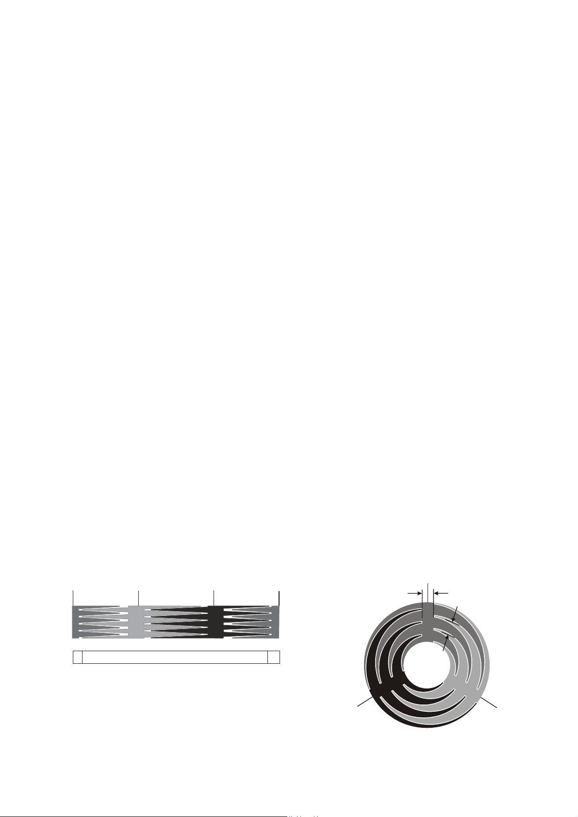
1.4 Slider and Wheel Construction
The QT1106 can connect to either a wheel or a linear slider
element (Figure 1.1). Selection of wheel or linear operation is
set through an SPI command. The basis of these designs is
found in US Patent 4,264,903 (expired).
The first and last positions of the linear slider have larger
touch areas.
As with touch button electrodes, wheels and sliders can be
constructed as etched areas on a PCB or flex circuit, or from
clear conductors such as Indium Tin Oxide (ITO) or screenprinted Orgacon™ (Agfa) to allow backlighting effects, or for
use over an LCD display.
1.5 QMagicTM Proximity Effect
Channel 7 of the QT1106 can optionally operate a ‘magic on’
function based on hand or body proximity to a product. By
using a relatively large electrode inside the product’s
enclosure and a larger value of Csb7 (see Figure 2.1), the
product can auto power up or activate its display with hand
approach. This simple feature can add enormous sales
appeal to almost any product.
1.6 SPI Interface
The QT1106 uses a five-wire SPI interface. In addition to the
standard four SPI signals (/SS, SCLK, MOSI and MISO),
there is a DRDY (data ready) output for flow control.
The QT1106 also provides a CHANGE signal to indicate
when there has been a change in detection state. This
removes the need for the host to poll the QT1106
continuously.
On each SPI transfer the host sends three bytes to the
QT1106 and the QT1106 simultaneously sends three bytes
to the host. The bytes sent from the host provide the QT1106
with all its configuration information; the bytes sent from the
QT1106 convey the key states.
(downloadable example CAD files for wheels and sliders can be found on the Quantum
SNSA3
0
SNSA1
Position (at 7 bits - 0 to 127)
Lq
Figure 1.1 All-Metal Slider and Wheel Construction
website,http://www.qprox.com/toolbox, then click QT1106)
Tips of triangles should be
spaced <=4mm apart.
<=4mm
Position 85
SNSA2
1 to 126
SNSA2
SNSA3
127
3 QT1106_8IR0.06_0407
Position 0
SNSA3
<=4mm
Position 43
SNSA1
Page 4

1.7 Basic Power Modes
1.7.1 Overview
The device features a number of modes to set the current
drain and speed of response.
The available operating modes are:
• Free Run - fastest detection response at all times
• LP mode - low power, slower touch sensing response
• Sleep - microamp-level current drain
• Sync mode - for noise suppression of low frequencies
1.7.2 Free Run Mode
This mode uses a continuous stream of acquire bursts. Free
Run mode has, in consequence, the highest power drain of
all the QT1106 operating modes but the fastest response
time.
1.7.3 LP Mode
In LP (low power) mode, the QT1106 spends most of the
time sleeping to conserve power; it wakes itself periodically to
perform acquire bursts, then normally goes back to sleep
again.
The QT1106 provides a choice of intervals between acquire
bursts to allow an appropriate speed/power trade-off to be
made for each product.
1.7.4 Sleep Mode
In Sleep mode, the QT1106 shuts down to conserve power; it
will remain in this mode forever or until the host wakes it
using the /SS pin.
1.7.5 Sync Mode
In this mode the device will synchronize to the host in a way
that allows for the suppression of heavy low frequency noise;
for example, from mains frequencies and their harmonics.
2 Signal Processing
2.1 Power-up Self-calibration
On power-up or after reset, all 10 channels are typically
calibrated and operational within 650ms.
2.2 Drift Compensation
This operates to correct the reference level of each key
automatically over time; it suppresses false detections
caused by changes in temperature, humidity, dirt and other
environmental effects.
2.3 Detection Integrator Filter
Detect Integrator (DI) filter confirmation reduces the effects of
noise on key states. The DI mechanism requires a specified
number of measurements that qualify as detections (and
these must occur in a row) or the detection will not be
reported.
In a similar manner, the end of a touch (loss of signal) also
has to be confirmed over several measurements. The
QT1106 provides a choice of either two or six DI
measurements for confirming start of touch; end of touch
always uses two measurements.
The DI mechanism works together with spread spectrum
operation to dramatically reduce the effects of noise.
2.4 AKSTM Adjacent Key Suppression
This patented feature works to prevent multiple keys from
responding to a single touch. This can happen with closely
spaced keys, or a scroll wheel that has buttons very near it.
AKS operates by comparing signal strengths from keys within
a group of keys to suppress touch detections from those that
have a weaker signal change than the dominant one.
When enabled globally on the QT1106, AKS allows only one
independent key, or the scroll section, to indicate a touch at a
time. Additionally, the QT1106 has options for partial AKS;
where some keys are included in the AKS operation and
others are not affected. In this case only one key in the AKS
group can indicate a touch at any time; other keys can
indicate touch in any combination.
AKS can also be disabled.
2.5 Autorecalibration (MOD)
The device can time out and recalibrate each key
independently after a continuous touch detection that lasts for
the chosen ‘Maximum on-duration’ (MOD). This ensures that
a key can never become ‘stuck on’ due to foreign objects or
other external influences.
After recalibration the key will continue to function normally.
The nominal delay is selectable to be either 10s, 20s, 60s, or
infinite (disabled), though the actual delay is different in some
operating modes (see Table 2.1).
Table 2.1 Maximum On-duration
Max on-durationsOperating Mode
10s, 20s, 60sFree Run
LP mode,
200ms1 response (120ms2)
LP mode,
1
280ms
LP mode,
440ms1 response (360ms2)
LP mode,
760ms
(typ 55Hz sync)
1
response times are estimated using a DI of six counts.
2
response times are estimated using a DI of two counts.
Note: all response times are based on typical sense
capacitor values.
The device also autorecalibrates all keys when one or more
normal keys’ signal reflect a sufficient decrease in
capacitance from the reference level (signal error). If QMagic
Proximity mode is active, a signal error on the Proximity Key
(Key 7) will only recalibrate itself. This is filtered in a manner
similar to the DI filter; the decrease in capacitance must be
seen for at least six successive cycles. Hence, in Free Run
mode the device typically recalibrates within 400ms so as to
recover normal operation quickly.
response (200ms2)
1
response (680ms2)
10s, 20s, 60s
10s, 20s, 60s
15s, 30s, 88s
28s, 55s, 164s
10s, 20s, 60sSync mode
(vary with sync rate)
n/aSleep mode
Lq
4 QT1106_8IR0.06_0407
Page 5

2.6 QMagicTM Proximity Sensor
Key 7 (SNSB7) can be optimized for operation as a hand
proximity sensor via the serial interface (see Section 3.5.2,
Prox = 1). The proximity sensitivity of channel 7 can be
increased by a higher value of Cs. The AKS mode should be
set to mode 101, to ensure that the proximity key does not
lock out other keys or the wheel/slider.
Note that proximity fields are often unstable especially in
products that can move around, such as mobile phones and
MP3 players. In particular, the proximity channel can stick on
after a detection. As soon as possible after proximity
channel 7 becomes active, it should be recalibrated via the
serial interface (see Section 3.5.2, CalK = 1, Cal Key Num
bits = 111) in order to clear the proximity channel.
Design of proximity electrodes requires care, so as to ensure
that the electrode area is maximized whilst ensuring
adequate and easy coupling to a hand as it approaches the
equipment.
2.7 Faulty and Unused Keys
Any sense channel that does not have its sense capacitor
(Cs) fitted is assumed to be either faulty or unused. This
channel takes no further part in operation unless a
host-commanded recalibration operation shows it to have an
in-range burst count again.
This is important for sense channels that have an open or
short circuit fault across
cause very long acquire bursts, and in consequence would
slow the operation of the entire QT1106.
Cs. Such channels would otherwise
Lq
5 QT1106_8IR0.06_0407
Page 6

2.8 Wiring
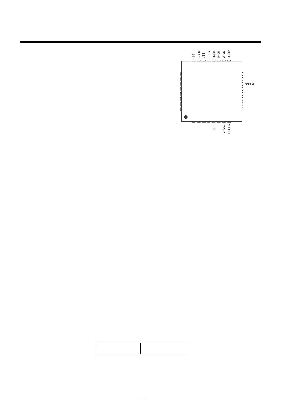
Table 2.2 Pinlist
32-QFN
Pin
Oscillator current driveIOSC4
16
Pin Type
I/O CMOS input/output
I CMOS input only
OD CMOS open drain output (pull up to Vdd)
OF CMOS output that can float during Reset, Sleep or LP modes
P Ground or power
Resistor to Vdd and optional
spread-spectrum RC network
If UnusedNotesFunctionTypeName
Open-Spread-spectrum driveODSPREAD1
VddActive low resetReset inputI/RST2
-+2.8 to +5.0VPowerPVdd3
-
-Leave open--n/c5
-To hostState change notificationOFCHANGE6
OpenSense pinTo Csb7I/OSNSB77
OpenSense pinTo Csb6I/OSNSB68
OpenSense pinTo Csb5I/OSNSB59
OpenSense pinTo any Csb + KeyI/OSNSB10
OpenSense pinTo any Csb + KeyI/OSNSB11
OpenSense pinTo any Csb + KeyI/OSNSB12
OpenSense pinTo any Csb + KeyI/OSNSB13
OpenSense pinTo Csb4I/OSNSB414
OpenSense pinTo Csb3I/OSNSB315
OpenSense pinTo Csb2I/OSNSB2
OpenSense pinTo Csb1I/OSNSB117
OpenSense pinTo any Csb + KeyI/OSNSB18
OpenSense pinTo any Csb + KeyI/OSNSB19
OpenSense pinTo any Csb + KeyI/OSNSB20
-SPI handshake lineSPI Data ReadyOFDRDY21
--GroundPVss22
-SPI serial bit clockSPI ClockISCLK23
-Idle high, slave select lineSPI Slave Select inI/SS24
-Data from host to QT1106SPI Master Out /Slave InIMOSI25
-Data from QT1106 to hostSPI Master In / Serial OutOFMISO26
OpenSense pinTo any Csa + wheel/sliderI/OSNSA27
OpenSense pinTo any Csa + wheel/sliderI/OSNSA28
OpenSense pinTo any Csa + wheel/sliderI/OSNSA29
OpenSense pin position 43To Csa1I/OSNSA130
OpenSense pin position 85To Csa2I/OSNSA231
OpenSense pin position 0To Csa3I/OSNSA332
Note: Sense terminals can be twinned with any sense drive terminals of the same group, e.g. SNSA1 can be
paired with any SNSA terminal.
Suggested regulator manufacturers:
• Toko (XC6215 series)
• Seiko (S817 series)
• BCDSemi (AP2121 series)
Re Figure 2.1 check the following sections for the variable component values:
• Section 6.3, page 13: Cs capacitors (Csb)
• Section 6.4, page 14: Sample resistors (R
SNS
)
• Section 6.6, page 14: Voltage levels
• Page 7: Css capacitor
Lq
6 QT1106_8IR0.06_0407
Page 7
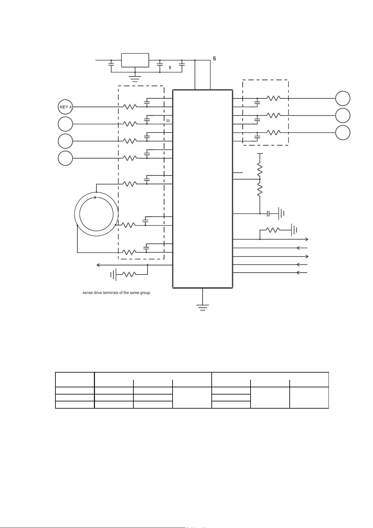
Vunreg
KEY 3
KEY 2
KEY 1
The wheel shows positions at
7-bit resolution. See the table
at the end of Section 3.5.2 for
other resolutions.
CHANGE out
Sense terminals can be twinned with any
NOTE:
e.g. SNSA1 can be paired with any SNSA terminal.
SNSA pins: 27 ,28, 29
SNSB pins: 10, 11, 12, 13, 18, 19, 20
127 0
Figure 2.1 Connection Diagram (32-QFN Package)
VDD
Note: One bypass capacitor to be
tightly wired between Vdd and Vss.
Follow recommendations from regulator
manufacturer for input and output
capacitors.
2
/RST
SNSB
SNSB7
SNSB
SNSB6
SNSB
SNSB5
QT1106
4.7uF
Voltage Reg
Keep these parts
close to the IC
R
SNSB4
R
SNSB3
R
SNSB2
R
SNSB1
4.7uF 100nF
14
C
Sb4
C
Sb3
C
Sb2
C
Sb1
SNSB4
13
SNSB
15
SNSB3
SNSB
16
SNSB2
19
SNSB
17
SNSB1
18
SNSB
3
VDD
32-QFN
32
R
SNSA3
R
4385
SNSA1
R
SNSA2
100K
C
Sa3
C
Sa1
C
Sa2
27
30
29
31
28
6
SNSA3
SNSA
SNSA1
SNSA
SNSA2
SNSA
CHANGE
VSS
22
N.C.
OSC
SPREAD
DRDY
SCLK
MISO
MOSI
/SS
12
C
7
11
C
8
10
C
9
5
4
1
21
23
26
25
24
Keep these parts
close to the IC
Sb7
Sb6
Sb5
VDD
**Rb1
**
See the table below for
suggested resistor and capacitor
values, with and without spread
spectrum.
**Rb2
No Spread-spectrum:
Replace Css with 100k resistor and remove Rb2
*
Css
R
R
R
100k
SNSB7
KEY 7
SNSB6
KEY 6
SNSB5
KEY 5
SPI DRDY out
SPI SCLK in
SPI MISO out
SPI MOSI in
SPI /SS in
IMPORTANT DESIGN GUIDELINES:
• The sensitivities of the various sense channels are determined by the values of the respective Cs
capacitors (i.e. Csb1,
Csb7, etc.); these values will require adjustment based on building a prototype product and testing the sensitivity
experimentally.
• Rb1, Rb2 sets the oscillator frequency; recommended values are:
Without Spread SpectrumWith Spread SpectrumVdd Range
CssRb2Rb1CssRb2Rb1
27k12k< 3 V
see note
below
15k
18k22k12k3.0~3.6V
20k27k15k> 3.6V
not fitted
replace with
100k resistor
• The required value of the spread-spectrum capacitor (Css) will vary according to the lengths of the acquire bursts. A
typical value is 100nF-220nF.
• When the QT1106 is running the OSC pin has a DC voltage typically between 1V and 1.5V; the use of spread
spectrum will cause a small low-frequency variation in the voltage. The internal oscillator signal is not visible on this
pin.
• Signals DRDY and CHANGE may need pull-down resistors, see Section 5 on page 13.
Lq
7 QT1106_8IR0.06_0407
Page 8
3 SPI Interface
3.1 Introduction
The QT1106 is an SPI slave mode device. This section
describes the hardware operation of this interface.
3.2 CHANGE Pin
The QT1106 has a CHANGE output pin which allows for key
state change notification. Use of the CHANGE signal relieves
the host of the burden of regularly polling the QT1106 to get
key states. CHANGE goes high when there is a change of
state, i.e. when a new key is pressed, or released, or a
movement is detected on the wheel/slider.
CHANGE also goes high after a reset to indicate to the host
that it should do an SPI transfer in order to provide initial
configuration information to the QT1106 (as it does on every
SPI transfer).
CHANGE goes low after the status is read through an SPI
transfer.
3.3 SPI Parameters
The SPI transmission parameters are:
• 70kHz max clock rate
• 8 data bits
• 6.7µs min low clock period
• 6.7µs min high clock period
• Three bytes per transmission, byte 1 most significant
bit sent first
• Clock idle high
• Shift out on falling edge
• Shift in on rising edge
The host must always transfer three bytes in succession
within the allotted time (10ms maximum). If all bytes are not
received in this interval it is treated by the QT1106 as an
error and the DRDY line will go low before the transmission is
completed.
Messages from the host to the QT1106 carry configuration
information; return data from the QT1106 carries key state
information. For details of the message contents see
Sections 3.5 and 3.6.
3.4 SPI Operation
The basic timing diagram for SPI operation is shown in
Figure 3.1 The host does the clocking and controls the timing
of the transfers, subject to Data Ready (DRDY), from the
QT1106. Transfers are always clocked as a set of three
bytes, Byte 1, 2 and 3.
The host should not attempt to clock the SPI bus to the
device while DRDY is low; during DRDY low the QT1106 is
busy and will ignore SPI activity, with the exception of a 20µs
grace period after the fall of DRDY, where there are no
communications during the high period of DRDY.
Note: DRDY can only become active (go high) if /SS is held
high when idle.
DRDY stays high for at least 450µs. It falls again after Byte 3
has shifted to indicate completion. After the fall of DRDY, the
device acquires (bursts). DRDY goes high to permit SPI
activity after each burst.
After the host asserts /SS low, it should wait >22µs before
starting SCLK. The QT1106 reads the MOSI pin with each
rising edge of SCLK, and shifts data out on the MISO pin on
falling edges. The host should do the same to ensure proper
operation.
Between the end of the Byte 1 shift and the start of the Byte 2
shift (and between Byte 2 and Byte 3), the host may raise
/SS again, but this is not required; the QT1106 ignores /SS
during transfer of the three bytes.
All timings not mentioned above should be as in Figure 3.1.
Acquire Bursts
DRDY from QT
/SS from host
SCLK from Host
Host Data Ou tp u t
(QT1106 Input - MOSI)
QT Data Outpu t
(QT1106 Out - MISO)
/SS pulse during 20us grace period
DRDY from QT
/SS from host
Lq
Figure 3.1 SPI Operation
~23ms
<470us
<10ms
>22us /SS m ay go high between between byt e s ; <5.7us
>6.7us >10.8us
>6.7us
Data sam ple d on ri sing edge
Data shifts out on falling
147 15674326
32
Command By te 1 Command By te 2 Command By te 3
3-state 3-state
>450us
(grace period)
Response B yte 1 Response Byte 2 Response B yte 3
?0576543210
<17us
<20us
bytes; QT1106 ignores this QT1106 ignores thi s
76
5
0
01
234567
/SS may go high
>0us
>0us
don't caredon't care don't care don't care
12 0
34
>0ns <500ns
01234567
8 QT1106_8IR0.06_0407
240ms
don't care
Page 9

/SS Wake Operation: /SS is also used to wake the device
from sleep, see Section 4.3
3.5 SPI Host Commands
3.5.1 Overview
The command from the host consists of three bytes, #1, #2
and #3. These three bytes contain operation mode settings
which must be transmitted every time. The setting information
in these three bytes becomes effective immediately after all
three are received by the QT1106.
The response to these three bytes are three data bytes
containing key detection information.
A downloadable host-driver software example for controlling
the QT1106 can be found on the Quantum website at
http://www.qprox.com/toolbox,
There are two command modes, selectable through bit CT.
CT - Custom threshold: Selects between normal command
bytes and custom threshold commands.
CT = 0: Normal commands.
CT = 1: Custom Threshold commands.
3.5.2 Normal Command Mode
When CT = 0, the three host command bytes should contain
the following bits:
Byte #
1
2
3
Bits labelled ‘0’ should not be altered.
The bits used in these three bytes are defined as follows:
AKS - Three bits used to determine the AKS mode. See
Section 2.4 for further information.
AKS
1
keys 1-4 AKS’d together
2
keys 5-7 AKS’d together
3
keys 1-6 AKS’d together
SLD - Scrolling device type selection.
SLD = 0: Wheel mode (default)
SLD = 1: Linear slider mode.
Prox - Key 7 QMagic Proximity mode. See Section 2.6 for
further information.
Prox = 0: Key 7 is a normal key (default)
Prox = 1: Key 7 is a proximity sensor.
Note: Once activated, Key 7 will be in QMagic Proximity
mode until a reset occurs.
Mode - These bits determine the Sleep / Low Power modes
the device runs in.
0
AKS Option
012
000
AKS disabled (default)
AKS global100
AKS keys + Wheel/Slider010
AKS 4 keys
AKS 4 keys
AKS (6 keys
then click QT1106.
BitHost
1
+ 3 Keys2 + Wheel/Slider110
1
+ (3 Keys2 + Wheel/Slider)001
3
+ Wheel/Slider) + key 7101
01234567
AKSSLDProx00CT=0
ModeLPBDIMOD
Cal Key NumCalKCalWResolution
Mode Bits
Operating Mode
012
000
Free Run (default)
LP mode, 200ms
LP mode, 280ms
LP mode, 440ms
LP mode, 760ms
1
response time (120ms2)100
1
response time (200ms2)010
1
response time (360ms2)110
1
response time (680ms2)001
Sync mode101
Sleep011
(reserved)111
1
response times are estimated using a DI of six counts.
2
response times are estimated using a DI of two counts.
LPB - Sets the LP mode ‘following burst’ option. See
Figures 4.1 and 4.2.
LPB = 0: If the host communicates with the device or there
is an /SS pulse during any LP mode (modes 001 to
100), there will be no following burst. The only bursts
that will take place are those that occur as naturally
defined by the LP mode noted above.
LPB = 1: If the host communicates with the device or there
is an /SS pulse during any LP mode (modes 001 to
100), there will be an additional burst following /SS
raising high. (default)
DI - Set the ‘Detect Integrator’ noise filter function.
DI = 0: Two detections required to confirm a touch (faster
but less noise immune).
DI = 1: Six detections required to confirm a touch (slower
but more noise immune; appropriate for most
applications). (default)
MOD (Recal Time) - Sets the 'Maximum On-duration' for all
keys. Controls the time from the start of a key detection to
when the key is automatically recalibrated. See Table 2.1
for MOD times in other operating modes.
MOD
Maximum On-duration in Free Run Mode
56
00
10s (default)
20s10
60s01
infinite MOD - timeout disabled11
Cal Key Num - key to be recalibrated when CalK = 1.
Cal Key
Num Bits
Key
012
Recalibrate all keys (excluding wheel/slider)000
Recalibrate Key 1100
Recalibrate Key 2010
Recalibrate Key 3110
Recalibrate Key 4001
Recalibrate Key 5101
Recalibrate Key 6011
Recalibrate Key 7111
CalK - Recalibrates the key(s) specified by Cal Key Num.
CalK = 0: No recalibration (normal state of this bit).
CalK = 1: The device recalibrates key(s).
CalW - Recalibrates the wheel/slider.
CalW = 0: No recalibration (normal state of this bit).
CalW = 1: The device recalibrates the wheel/slider.
Lq
9 QT1106_8IR0.06_0407
Page 10
Set CalK/CalW only once when required, and set CalK/CalW
= 0 thereafter. If the bit is constantly set to 1, the device will
keep recalibrating and will become non-responsive.
Note that the device recalibrates automatically on power-up,
so that the use of Recal should rarely be required excepting
Key 7 when used as a proximity sensor, in which case this
channel should be recalibrated soon after each proximity
detection to ensure stability.
Resolution - the resolution of the wheel/slider’s reported
position. Refer to Figure 3.2.
Resolution
Bits
Resolution
567
Reserved
000
2 Bits : 4 positions (0...3)100
3 Bits : 8 positions (0...7)010
4 Bits : 16 positions (0...15)110
5 Bits : 32 positions (0...31)001
6 Bits : 64 positions (0...63)101
011
7 Bits : 128 positions (0...127) (default)
8 Bits : 256 positions (0...255)111
Note: a resolution change will only become effective on the
next touch.
3.5.3 Custom Threshold Command Mode
When CT = 1, the three host command bytes should contain
the following bits:
BitHost
Byte #
1
2
T1 - Wheel/Slider Threshold
3
T1: Custom threshold value of the wheel/slider. Higher
numbers are less sensitive. Touch detection uses this
threshold combined with a hysteresis equal to 12.5 percent of
the threshold (with a minimum hysteresis value of one).
Power-up default setting: 40
01234567
0000000CT=1
00000000
Note: Custom Threshold Command is only used if the
detection threshold of the wheel/slider needs to be changed
from the power-up default.
3.6 SPI Responses
The 3 return bytes which contain key states are as follows:
BitReturn
byte #
Position3
CTL: Custom Threshold Loaded: If CTL = 1, a custom
wheel/slider threshold has been loaded from the host. If a
custom threshold is utilised, CTL can be used to indicate
if the threshold needs to be resent due to a reset of the
device.
QM: QMagic Proximity Mode: If QM = 1, QMagic Proximity
mode is activated (see Section 2.6).
LPS: LP / Sleep State: If LPS = 1, the device was in LP,
Sync, or Sleep mode when the requesting command was
received. If LPS = 0, the device was in Free Run mode.
EK: Key(s) in Error: If EK = 1, there is a sufficient decrease
in capacitance of one or more normal key(s) from the
reference level. All keys will be recalibrated if this
condition is seen for six successive cycles. If QMagic
Proximity mode is active, an error on the Proximity Key
(Key 7) will only cause a recalibration on itself.
EW: Wheel/Slider in Error: If EW = 1, there is a sufficient
decrease in capacitance of the wheel/slider from the
reference level. The wheel/slider will be recalibrated if this
condition is seen for six successive cycles.
CK: Key(s) in Calibration: If CK = 1, one or more key(s) are
being calibrated.
CW: Wheel/Slider in Calibration: If CW = 1, the
wheel/slider is being calibrated.
01234567
CTL0QMLPSEKEWCKCW1
K1K2K3K4K5K6K7W2
Slider Mode
SNSA
A3
2 bits
SNSA
A3
3 bits
4 bits
0
SNSA
A3
03
Note
: the first and last slider positions
(shaded) have larger touch areas.
SNSA
A1
0
SNSA
A1
12 4
SNSA
A1
12
4
Lq
Figure 3.2 Wheel and Slider Resolution
SNSA
A2
12
SNSA
A2
3
5
6
78910
5
SNSA
A2
11 121314
(see end of Section 3.5.2)
SNSA
A3
3
SNSA
A3
7
6
SNSA
A3
15
SNSA
A2
6
5
10 QT1106_8IR0.06_0407
SNSA
A3
7
4
3 bits
0
3
SNSA
A2
1
2
SNSA
A1
Wheel Mode
SNSA
A3
3
2
2 bits
0
1
SNSA
A1
SNSA
A3
15
0
14
1
SNSA
A2
13
12
11
10
9
4 bits
2
3
4
5
SNSA
6
78
A1
Page 11

K1...K7: Contains the key states of each key. A ‘1’ in a bit
position means the key is confirmed as being touched.
W: The state of the wheel/rotor. A ‘1’ means the wheel/slider
is confirmed as being touched.
Position: The position of touch on the wheel/slider. If the
wheel/slider is not being touched, the position will be the
position of the last touch.
4 Operating Modes
4.1 Introduction
Four basic operating modes are possible: Free Run, LP (Low
Power), Sync and Sleep. Sleep is a special case of LP mode,
where the sleep time is infinite. Sync is a special case of LP
mode which acts as a noise filter over successive /SS pulses
rather than temporarily operating as in Free Run mode.
4.2 Free Run Mode
In this mode the device operates continuously with short
intervals between burst groups; there are three bursts, one
burst for each electrode group. Between burst sets, DRDY
goes high for 450µs to allow SPI communications.
In this mode, the acquisition bursts are unsynchronized,
making this mode unsuitable if synchronization to mains
frequency is needed.
4.3 LP Mode
LP mode is designed to allow low power operation while still
retaining basic operation but at a slower speed. This mode is
useful for devices that must use the touch keys to wake up a
product, yet be in a low power mode.
Several LP timings allow the user to trade power versus
response time: the slower the response time, the lower the
power consumed.
In LP mode, the device spends most of the time sleeping
between bursts; it wakes itself periodically to do a set of three
acquisition bursts, then goes back to sleep.
If a touch is detected, the device operates as in Free Run
mode and attempts to perform the DI (detect integrator noise
filter) function to completion; if the DI filter fails to confirm a
detection the device goes back to sleep and resumes LP
mode. During the DI function the LPS bit will be cleared.
If a key is found to be in detection the CHANGE pin will go
high and the part will remain in Free Run mode. To go back
into LP mode the host has to request LP mode again.
CHANGE Pin in LP Mode: During the sleep portion of LP
mode, CHANGE is held low.
If however a change of key state is confirmed, CHANGE
goes high and the part runs from then on in Free Run mode
until the host reads the key state and puts the device back
into LP mode or some other mode.
MISO in LP Mode: During the sleep portion of LP mode,
MISO floats.
DRDY during LP Mode: DRDY remains high while the
QT1106 is sleeping, to indicate to the host that SPI
communications are possible. In LP mode, the host should
wake the QT1106 using a pulse on /SS before transferring
data over SPI (see below). During an actual acquire burst,
DRDY is held low.
/SS Wake Pulse in LP Mode: In LP mode the host should
wake the device from sleep using a low pulse on /SS. The
pulse should be at least 125µs wide.
Within 100µs of the end of the /SS pulse, the QT1106 will
take DRDY low for at least 40µs to indicate that it has
received the /SS wake pulse.
Following the >45µs DRDY low pulse, the host can
communicate normally with the device (see ‘Command
During LP Mode’ on Page 12).
If the LPB bit (page 9) is set, the device will then perform a
set of acquire bursts during which DRDY will be low.
Provided no key is detected as being touched during that
burst, the QT1106 will go back to sleep, leaving DRDY high.
The CHANGE pin can go high if a key state changes during
the burst(s) following the wake pulse.
If a key is confirmed as touched, the device will transition to
Free Run mode automatically.
Acqui r e Bursts
DRDY from QT
/SS from host
SCLK from Host
Host Data Ou tp u t
(QT1106 Input - MOSI)
QT Data Output
(QT1106 O u t - M I SO)
>40us <240us <240us
<150us
Lq
Figure 4.1 LP Mode SPI Operation with LPB = 1
No SPI Communication
~23ms ~23ms
>450us
<100us <470us
>125us
don't car e don't caredon't car e
don't car e don't care
3-state 3-state
<20us
(grace pe ri od )
/SS timing as left
don't care
don't care
SPI Communication
command bytes
response bytes
11 QT1106_8IR0.06_0407
Page 12

Command During LP Mode: First read ‘/SS Wake Pulse in
LP Mode’, on Page 11. Following DRDY rising at the end of
the 45µs low pulse, the host may perform a normal SPI
transfer as shown in Figure 3.1. The SPI transfer may start
while DRDY is high (450µs), and for a 20µs grace period
thereafter.
After the SPI transfer is completed, the QT1106 will generate
a set of three acquire bursts if LPB = 1, during which DRDY
will be low.
The mode and options settings sent from the host to the
QT1106 during the SPI transfer take effect after the set of
acquire bursts.
• If Free Run mode is selected, the QT1106 will take
DRDY high to indicate the possibility of an SPI
transfer.
• If either LP mode or Sleep mode is selected, the
QT1106 will go back to sleep with DRDY high
provided no key is detected as possibly touched.
• If Sync mode is selected, the QT1106 will go back to
sleep with DRDY high provided no key is detected as
possibly touched.
The CHANGE pin will go high at this time if a key is
confirmed as touched.
4.4 Sleep Mode
Sleep mode offers the lowest possible current drain, in the
low microamp region.
Sleep mode is a special case of LP mode, where the sleep
duration between bursts is infinite. All comments concerning
LP mode, including about SPI communications, apply equally
to Sleep mode, except that the LPB bit is ignored and bursts
are always generated after an SPI transfer or /SS wake
pulse as if LPB = 1.
Note that in Sleep mode the QT1106 only performs
acquisition bursts following being woken by /SS. This has two
effects.
• Touch detection only occurs following /SS-wake
pulses, and hence CHANGE can only go high at that
time.
• The QT1106 cannot drift its internal references unless
the host sends periodic /SS wake pulses. If the host
does not do this, then it should command the QT1106
to recalibrate when it sets the QT1106 into a different
operating mode.
This mode can be used by the host to create its own ‘LP
Mode’ timings via the /SS wakeup pulse method.
4.5 Sync Mode
This mode is useful for low frequency noise suppression, for
example from mains frequencies in line-operated appliances.
Acquisition bursts are synchronized to the /SS-wake pulses
from the host.
Sync mode is very similar to ‘LP 760ms response time’
mode, with two differences:
• It does not operate as in Free Run mode when a
touch is first detected
• The LPB bit is ignored and a burst is always
generated after each /SS wakeup or SPI transfer as if
LPB = 1
Not operating as in Free Run mode when a touch is first
detected (before DI confirmation has taken place) means that
acquisition bursts are restricted to the immediate time after a
sync signal (/SS), heightening the effect of low frequency
noise suppression.
In many applications of Sync mode the DI filter will need to
be set to two counts, to avoid the QT1106 response time
being unacceptably lengthened as a consequence of this.
Acqui r e Bursts
DRDY from QT
/SS from host
SCLK from Host
Host Data O u tp u t
(QT1106 Input - MOSI)
QT Data Ou tput
(QT1106 Out - MISO)
Figure 4.2 LP Mode SPI Operation with LPB = 0
No SPI Communication
>40us >70us
<150us <200us
<100us <470us
>125us
/SS t i m i ng as left
don't care don't caredon't care
don't care don't care
3-state 3-state
don't care
don't care
SPI Communication
command bytes
response bytes
Lq
12 QT1106_8IR0.06_0407
Page 13

5 Reset
5.1 Introduction
When starting from power-up or /RST reset there are a few
additional factors to be aware of. In most applications the
host will not need to take special action.
During hardware reset all outputs are disabled. To define the
levels of the CHANGE and DRDY during reset these signals
should pulled down by resistors to 0V. Otherwise, they may
drift high causing the host to detect a false logic 1.
When the initial reset phase ends, CHANGE and DRDY
outputs are enabled. DRDY will drive low and CHANGE will
drive high.
5.2 Delay to SPI Functionality
The QT1106 SPI interface is not operational while the device
is being reset. However, SPI is made operational early in the
start-up procedure.
After any reset (either via the /RST pin or via power-up), SPI
typically becomes operational within 100ms of /RST going
high or power-up. This is indicated to the host by DRDY
being pulsed high for at least 450µs, as occurs between
groups of acquire bursts when in Free Run mode. The
maximum delay is:
Vdd >= 4.5V: 150ms
Vdd < 4.5V: 200ms
5.3 Reset Delay to Touch Detection
After power up or reset, the QT1106 calibrates all electrodes.
During this time, touch detection cannot be reported. Four
dummy bursts are performed in 80ms after exiting from the
reset start-up delay. Calibration completes after 14 burst
cycles, which normally requires an additional 280ms.
In total, 460ms are required from reset or power-up for the
device to be fully functional.
Disabled Keys: Keys with missing Cs capacitors, or that
otherwise have an out-of-range signal during calibration, are
considered to be unused or faulty and are disabled. Disabled
keys are re-examined for operation after each reset or
recalibration event.
5.4 Mode Setting After Reset
After a reset the device will enter Free Run mode, with AKS
disabled.
6 Design Notes
6.1 Oscillator Frequency
The oscillator uses an external network connected to the
OSC and SPREAD pins as shown in Figure 2.1. The charts
in this figure show the recommended values to use
depending on nominal operating voltage and
spread-spectrum mode.
If spread-spectrum mode is not used, only resistor R
be used, the Css capacitor eliminated, and the SPREAD pin
pulled to Vss with a 100k resistor.
An out-of-specification oscillator can induce timing problems
such as large variations in response times as well as on the
SPI port.
B1
should
6.2 Spread-spectrum Circuit
The QT1106 offers the ability to spectrally spread its
frequency of operation to heavily reduce susceptibility to
external noise sources and to limit RF emissions. The
SPREAD pin is used to modulate an external passive RC
network that modulates the OSC pin. OSC is the main
oscillator current input. The circuit and recommended values
are shown in Figure 2.1.
The resistors Rb1 and Rb2 should be changed, depending
on Vdd. As shown in Figure 2.1, three sets of values are
recommended for these resistors, depending on Vdd. The
power curves in Section 7.6 also show the effect of these
resistors.
The spread-spectrum circuit can be eliminated if it is not
desired; see Section 6.1. Non spread-spectrum mode
consumes less current in the low power modes.
The spread-spectrum RC network should be adjusted to suit
the acquire burst lengths. The sawtooth waveform observed
on SPREAD should reach a crest height as follows:
Vdd >= 3.6V: 17 percent of Vdd
Vdd < 3.6V: 20 percent of Vdd
The Css capacitor connected to SPREAD (see Figure 2.1)
should be adjusted so that the waveform approximates the
above amplitude, ±10 percent, during normal operation in the
target circuit. If this is done, the circuit will give a spectral
modulation of 12 to 15 percent.
In cases where the three acquire bursts 1, 2, 3 are of
different lengths, the Css capacitor should be adjusted for the
longest acquire burst.
6.3 Cs Sample Capacitors - Sensitivity
The Cs sample capacitors accumulate the charge from the
key electrodes and determine sensitivity. Higher values of Cs
make the corresponding sensing channel more sensitive. The
values of Cs can differ for each channel, permitting
differences in sensitivity from key to key or to balance
unequal sensitivities.
Unequal sensitivities can occur due to key size and
placement differences and stray wiring capacitances. More
stray capacitance on a sense trace will desensitize the
corresponding key; increasing the Cs for that key will
compensate for the loss of sensitivity.
The Cs capacitors can be virtually any plastic film or low to
medium-K ceramic capacitor. The ‘normal’ Cs range is 1nF to
100nF for the keys and 4.7nF to 220nF for the wheel/slider,
depending on the sensitivity required; the larger values of Cs
require better quality to ensure reliable sensing. Acceptable
capacitor types for most uses include PPS film,
polypropylene film, and NP0 and X7R ceramics. Lower grade
ceramics than X7R are not advised; the X5R grade should be
avoided because it is less stable than X7R.
Lq
13 QT1106_8IR0.06_0407
Page 14

6.4 Rsns Resistors
Series resistors R
in-line with the electrode connections and are used to limit
electrostatic discharge (ESD) currents and to suppress radio
frequency interference (RFI). For most applications R
be in the range 4.7k to 33k each. In a few applications
with low loading on the sense keys the value may be up to
100k.
Although these resistors may be omitted, the device may
become susceptible to external noise or RFI. For details of
how to select these resistors see the Application Note
AN-KD02, downloadable from the Quantum website
http://www.qprox.com
Application Notes).
SNS
(R
SNSA
1...R
SNSA
3, R
SNSB
(go to the Support tab and click
1...R
SNSB
7) are
SNSB
will
6.5 Thermal Stability
The QT1106 can operate with or without the wheel/slider and
supports up to seven keys. Channels not fitted with a sense
capacitor will automatically be switched off during calibration.
For better thermal stability while operating with only one key,
it is best to fit a sense capacitor of the same type and value
for another spare key channel, in another burst group.
Additionally a small value Cx (~5pF COG) should be fitted to
simulate electrode capacitance.
The Cx value required for best thermal stability can be
obtained by matching the burst lengths of the key channel
and the dummy channel. The burst lengths of the channels
can be captured on an oscilloscope via the coin method, as
described in the Application note AN-KD02 (see Section 6.4).
This provides a stable reference for increased thermal
stability.
6.6 Power Supply
The power supply can range from 2.8 to 5.0 volts. If this
fluctuates slowly with temperature, the device will track and
compensate for these changes automatically with only minor
changes in sensitivity. If the supply voltage drifts or shifts
quickly, the drift compensation mechanism will not be able to
keep up, causing sensitivity anomalies or false detections.
The QT1106 power supply should be locally regulated using
a three-terminal device, to between 2.8V and 5.0V. If the
supply is shared with another electronic system, care should
be taken to ensure that the supply is free of digital spikes,
sags, and surges, all of which can cause adverse effects.
For proper operation a 0.1µF, or greater, bypass capacitor
must be used between Vdd and Vss; the bypass capacitor
should be routed with very short tracks to the QT1106's Vss
and Vdd pins.
6.7 PCB Layout and Construction
Refer to the Application Note AN-KD02 ‘Secrets of a
Successful QTouch Design’, downloadable from the
Quantum web site http://www.qprox.com
tab and click Application Notes) for information related to
layout and construction matters. Downloadable example CAD
files for wheels and sliders can also be found on the website)
The sensing channels used for the individual keys can be
implemented as per AN-KD02.
(go to the Support
Lq
14 QT1106_8IR0.06_0407
Page 15

7 Specifications
7.1 Absolute Maximum Specifications
Operating temperature, Ta............................................................................. -40 to +850C
Storage temp, Ts.....................................................................................-50 to +125
Vdd................................................................................................. -0.3 to +6.0V
Max continuous pin current, any control or drive pin............................................................ ±20mA
Short circuit duration to ground or Vdd, any pin.................................................................infinite
Voltage forced onto any pin................................................................. -0.3V to (Vdd + 0.3) Volts
7.2 Recommended Operating Conditions
Operating temperature, Ta............................................................................. -40 to +850C
Vdd.................................................................................................+2.8 to +5.0V
Short-term supply ripple+noise.............................................................................. ±5mV/s
Long-term supply stability.................................................................................. ±100mV
Cs range keys........................................................................................1nF to 100nF
Cs range wheel/slider............................................................................... 4.7nF to 220nF
Cx range................................................................................................0 to 50pF
7.3 AC Specifications
Vdd = 5.0V, Ta = recommended, Cx = 5pF, Cs keys = 4.7nF, Cs wheel/slider = 15nF, no spread-spectrum network,
Rb1 = 20k; circuit of Figure 2.1.
NotesUnitsMaxTypMinDescriptionParameter
From cold start
kHz125Burst center frequencyFc
ms
Vdd >= 4.5V
Vdd < 4.5V
ms280Recalibration timeTrc
Total deviation%15Burst modulation, percentFm
Keysµs2.33Sample pulse durationTpc
Total for all three acquire burst
ms20Acquire burst durationTbd
groups
ms120
ms40
280ms LP setting, DI = six countsms280Response time - LP modeTdl
End of touchms40Release time - all modesTdr
Tdf6
Tdf2
100Start-up to SPI timeTsu
150
200
Response time Free Run mode, DI 6 samples
Response time Free Run mode, DI 2 samples
0
C
7.4 DC Specifications
Vdd = 5.0V, Ta = recommended, Cx = 5pF, Cs keys = 4.7nF, Cs wheel/slider = 15nF, no spread-spectrum network,
Rb1 = 20k; circuit of Figure 2.1.
NotesUnitsMaxTypMinDescriptionParameter
Idd (FR)
Idd (LP280)
Idd (LP760)
Idd (Sleep)
Average supply current,
Free Run mode
Average supply current,
280ms LP mode
Average supply current,
760ms LP mode
Average supply current,
Sleep mode
Supply turn-on slopeVdds
2.2
1.9
1.6
1.3
mA83.6
Vdd = 5.0
Vdd = 4.0
Vdd = 3.6
Vdd = 3.3
Vdd = 2.8
Vdd = 3.0µA<165
Vdd = 3.0µA<75
Vdd = 3.0µA<6
V/s100
Required for start-up, w/o
external reset cct
V0.3Vdd0Low input logic levelVil
VVdd0.7VddHigh input logic levelVhl
7mA sinkV0.5Low output voltageVol
2.5mA sourceVVdd-0.5High output voltageVoh
µA±1Input leakage currentIil
bits14Acquisition resolutionAr
Lq
15 QT1106_8IR0.06_0407
Page 16

7.5 Signal Processing
Vdd = 5.0V, Ta = recommended, Cx = 5pF, Cs keys = 4.7nF, Cs wheel/slider = 15nF, no spread-spectrum network,
Rb1 = 20k; circuit of Figure 2.1
NotesUnitsValueDescription
Threshold for increase in Cx loadcounts10Detection threshold (keys)
Detection threshold
(wheel/slider)
Detection hysteresis
(wheel/slider)
DI filter, start of touch, normal
mode
DI filter, start of touch, fast DI
mode
Maximum On-duration
10, 20,
60,
infinite
counts2Detection hysteresis (keys)
samples2DI filter, end of touch
samples6Anti-detection filter
samples1Faulty channel filter
secs
Changeable through SPIcounts40
12.5 percent of wheel/slider detection threshold.counts5
Must be consecutive or detection failssamples6
Must be consecutive or detection failssamples2
Threshold for decrease of Cx loadcounts8Anti-detection threshold
In these modes: Free Run, 200ms LP, 280ms LP, Sync with 55Hz
sync
Lq
16 QT1106_8IR0.06_0407
Page 17

7.6 Idd Curves
Table 7.1 Typical Average Idd Curves (No Spread Spectrum)
Cs (keys) = 4.7nF, Cs (wheel) = 15nF Ta = 200, no spread-spectrum circuit (see Figure 2.1).
Rb1 = 20k ohms
Rb1 = 18k ohm s
Rb1 = 15k ohms
QT1106 Idd ( Free Run mode) mA
4.0
3.0
2.0
Idd (mA)
1.0
0.0
2.5 3 3.5 4 4.5 5 5.5
Vdd (V)
QT 1106 Idd (L P 280ms mo de) u A
750
600
450
300
Idd (uA)
QT 1106 Idd (L P 200ms mo de) u A
1250
1000
750
500
Idd (mA)
250
0
2.5 3 3.5 4 4.5 5 5.5
Vdd (V)
QT1106 I dd ( LP 440ms mode) uA
500
400
300
200
Idd (uA)
150
0
2.5 3 3.5 4 4.5 5 5.5
Vdd (V)
QT 1106 Idd (L P 760ms mo de) u A
250
200
150
100
Idd (uA)
50
0
2.5 3 3.5 4 4.5 5 5.5
Vdd (V)
100
0
2.5 3 3.5 4 4.5 5 5.5
Vdd (V)
QT1106 Idd (Sleep mode) uA
18
16
14
12
10
8
Idd (uA)
6
4
2
0
2.5 3 3.5 4 4.5 5 5.5
Vdd (V)
lQ 17 QT1106_8IR0.06_0407
Page 18

Table 7.2 Typical Average Idd Curves (Spread Spectrum)
Cs (keys) = 4.7nF, Cs (wheel) = 15nF Ta = 200, spread-spectrum circuit (see Figure 2.1).
Rb1 = 15k ohms, Rb2 = 27k ohm s, Css = 100nF
Rb1 = 12k ohms, Rb2 = 22k ohm s, Css = 100nF
Rb1 = 12k ohms, Rb2 = 27k ohm s, Css = 100nF
QT1106 Idd ( Free Run mode) mA
4.0
3.0
2.0
Idd (mA)
1.0
0.0
2.5 3 3.5 4 4.5 5 5.5
Vdd (V)
QT 1106 Idd (L P 280ms mo de) u A
750
600
450
300
Idd (uA)
QT 1106 Idd (L P 200ms mo de) u A
1250
1000
750
500
Idd (mA)
250
0
2.5 3 3.5 4 4.5 5 5.5
Vdd (V)
QT1106 I dd ( LP 440ms mode) uA
500
400
300
200
Idd (uA)
150
0
2.5 3 3.5 4 4.5 5 5.5
Vdd (V)
QT 1106 Idd (L P 760ms mo de) u A
250
200
150
100
Idd (uA)
50
0
2.5 3 3.5 4 4.5 5 5.5
Vdd (V)
100
0
2.5 3 3.5 4 4.5 5 5.5
Vdd (V)
QT1106 Idd (Sleep mode) uA
18
16
14
12
10
8
Idd (uA)
6
4
2
0
2.5 3 3.5 4 4.5 5 5.5
Vdd (V)
lQ 18 QT1106_8IR0.06_0407
Page 19
7.7 Mechanical Dimensions - 32-QFN Package
Dimensions In Millimeters
Symbol Minimum Nominal Maximum
A0.70 -0.95
A1 0.00 0.02 0.05
b 0.18 0.25 0.32
C - 0.20 REF D 4.90 5.00 5.10
D2 3.05 - 3.65
E 4.90 5.00 5.10
E2 3.05 - 3.65
e-0.50L 0.30 0.40 0.50
y0.00-0.075
Note:
there is no functional requirement for the large pad on the underside of the 32-QFN package to
be soldered to the substrate. If the final application does require this area to be soldered for
mechanical reasons, the pad(s) to which it is soldered to must be isolated and contained under the
32-QFN footprint only.
7.8 Part Marking
Pin 1 Identification
QT1106
©QRG 8I
YYWWG
run nr.
Two lines of text to ensure product traceability:
'YY' = Year of manufacture,
'WW' = Week of manufacture,
'G' = Green/RoHS Compliant,
'run nr.' = Run Number
QRG Part
Number
QRG
Revision
Code
lQ 19 QT1106_8IR0.06_0407
Page 20

7.9 Moisture Sensitivity Level (MSL)
SpecificationsPeak Body TemperatureMSL Rating
IPC/JEDEC J-STD-020C260OCMSL3
lQ 20 QT1106_8IR0.06_0407
Page 21

8 Datasheet Control
8.1 Changes
Changes this issue (datasheet issue 6)
Front page
Section 2.8.
Section 6.4, 6.5
Section 7.9
Section 8
Rear page
8.2 Numbering Convention
Part Number
Datasheet Issue Number
QT1106_MXN.nn_mmyy
Chip Revision
(Where M= Major chip revision,
N = Minor chip revision,
X = Prereleased Product
[or R = Released Product])
A minor chip revision (N) is defined as a revision change which does not affect product functionality or datasheet.
The value of N is only stated for released parts (R).
Datasheet Release Date;
(Where mm = Month, yy = Year)
lQ 21 QT1106_8IR0.06_0407
Page 22

lQ Copyright © 2006-2007 QRG Ltd. All rights reserved.
Patented and patents pending
Corporate Headquarters
1 Mitchell Point
Ensign Way, Hamble SO31 4RF
Great Britain
Tel: +44 (0)23 8056 5600 Fax: +44 (0)23 8045 3939
www.qprox.com
North America
651 Holiday Drive Bldg. 5 / 300
Pittsburgh, PA 15220 USA
Tel: 412-391-7367 Fax: 412-291-1015
The specifications set out in this document are subject to change without notice. All products sold and services supplied by QRG are
subject to QRG’s Terms and Conditions of sale and services. QRG patents, trademarks and Terms and Conditions can be found online at
http://www.qprox.com/about/legal.php. Numerous further patents are pending, one or more which may apply to this device or the
applications thereof.
QRG products are not suitable for medical (including lifesaving equipment), safety or mission critical applications or other similar
purposes. Except as expressly set out in QRG's Terms and Conditions, no licenses to patents or other intellectual property of QRG
(express or implied) are granted by QRG in connection with the sale of QRG products or provision of services. QRG will not be liable for
customer product design and customers are entirely responsible for their products and applications which incorporate QRG's produ cts.
Development Team: Lim Wei Jiun, Martin Simmons, Alan Bowens, Luben Hristov
 Loading...