

Page 1
lQ
This datasheet is applicable to all revision 3 chips
QT
OUCH
™ 10-KEY S
QT1103
ENSOR
IC
The QT1103 is designed for low cost appliance, mobile, and consumer
electronics applications.
QTouch™ technology is a type of patented charge-transfer sensing
SYNC/LP
DETECT
VSS
SNS7K
SNS7
SNS6K
SNS6
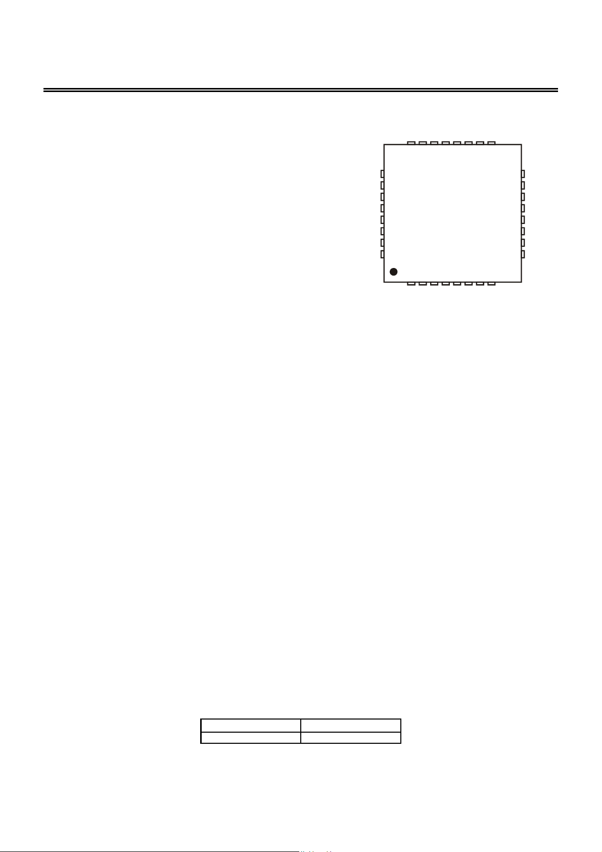
24 23 222120 19 18 17
SNS5K
method well known for its robust, stable, EMC-resistant characteristics.
It is the only all-digital capacitive sensing technology in the market
today. This technology has over a decade of applications experience
spanning thousands of designs.
QTouch circuits are renowned for simplicity, reliability, ease of design,
and cost effectiveness.
QTouch™ sensors employ a single reference capacitor tied to two pins
of the chip for each sensing key; a signal trace leads from one of the
pins to the sensing electrode which forms the key. The sensing
SNS8
SNS8K
SNS9
SNS9K
N/C
/CHANGE
1W
RX
25
26
27
28
29
30
31
32
QT1103
16
15
14
13
12
11
10
9
electrode can be a simple solid shape such as a rectangle or circle. An
LED can be placed near or inside the solid circle for illumination.
The key electrodes can be designed into a conventional Printed Circuit
Board (PCB) or Flexible Printed Circuit Board (FPCB) as a copper
12345
SS
VDD
OSC
/RST
67
N/C
8
SNS0
SNS1
SNS0K
pattern, or as printed conductive ink on plastic film.
AT A GLANCE
Number of keys: 1 to 10
Technology: Patented spread-spectrum charge-transfer (one-per-key mode)
Key outline sizes: 5mm x 5mm or larger (panel thickness dependent); widely different sizes and shapes possible
Key spacings: 6mm or wider, center to center (panel thickness, human factors dependent)
Electrode design: Single solid or ring shaped electrodes; wide variety of possible layouts
Layers required: One layer substrate; electrodes and components can be on same side
Substrates: FR-4, low cost CEM-1 or FR-2 PCB materials; polyamide FPCB; PET films, glass
†
Electrode materials: Copper, silver, carbon, ITO, Orgacon
Panel materials: Plastic, glass, composites, painted surfaces (low particle density metallic paints possible)
Adjacent Metal: Compatible with grounded metal immediately next to keys
Panel thickness: Up to 50mm glass, 20mm plastic (key size dependent)
Key sensitivity: Settable via change in reference capacitor (Cs) value
Outputs: RS-232 based
serial output, capable of single-wire operation
Moisture tolerance: Good
Power: 2.8V ~ 5.0V
Package: 32-pin 5 x 5mm QFN RoHS compliant
Signal processing: Self-calibration, auto drift compensation, noise filtering, AKS™
Applications: Portable devices, domestic appliances and A/V gear, PC peripherals, office equipment
Patents: AKS™ (patented Adjacent Key Suppression)
QTouch™ (patented Charge-transfer method)
†
Orgacon is a registered trademark of Agfa-Gevaert N.V
ink (virtually anything electrically conductive)
SNS5
SNS4K
SNS4
SNS3K
SNS3
SNS2K
SNS2
SNS1K
AVAILABLE OPTIONS
A
0
C to +850C
LQC
32-QFNT
QT1103-ISG-40
Copyright © 2006-2007 QRG Ltd
QT1103_3R0.03_0607
Page 2

Contents
1 Overview
1.1 Differences With QT1101
1.2 Parameters
1.3 Wiring
2 Device Operation
2.1 Reset and Startup Time
2.2 Option Resistors
2.3 DETECT Pin
2.4 /CHANGE Pin
2.5 SYNC/LP Pin
2.6 AKS™ Function Pins
2.7 MOD_0, MOD_1 Inputs
2.8 Fast Detect Mode
...........................................
1.2.1 Introduction
1.2.2 Burst Operation
1.2.3 Self-calibration
1.2.4 Autorecalibration
1.2.5 Drift Compensation
1.2.6 Detection Integrator Confirmation
1.2.7 Spread-spectrum Operation
1.2.8 Sync Mode
1.2.9 Low Power (LP) Mode
1.2.10 Adjacent Key Suppression (AKS™)
1.2.11 Outputs
1.2.12 Simplified Mode
.......................................
.....................................
.....................................
.......................................
...........................................
......................................
......................................
2.5.1 Introduction
2.5.2 Sync Mode
2.5.3 Low Power (LP) Mode
......................................
.....................................
.....................................
..............................
...................................
...................................
..................................
.................................
........................
............................
...............................
......................
..................................
....................................
...............................
....................................
...............................
.................................
...............................
...................................
2.9 Simplified Mode
3
2.10 Unused Keys
3
2.11 Serial 1W Interface
3
3
3
3
3
3
3
3
3
3
4
4
4
5
8
8
8
8
8
8
8
8
8
9
9
9
2.11.1 Introduction
2.11.2 Basic 1W Operation
2.11.3 LP Mode Effects on 1W
2.11.4 2W Operation
3 Design Notes
3.1 Oscillator Frequency
3.2 Spread-spectrum Circuit
3.3 Cs Sample Capacitors - Sensitivity
3.4 Rsns Resistors
3.5 Power Supply
3.6 PCB Layout and Construction
4 Specifications
4.1 Absolute Maximum Specifications
4.2 Recommended Operating Conditions
4.3 AC Specifications
4.4 DC Specifications
4.5 Signal Processing
4.6 Idd Curves
4.7 LP Mode Typical Response Times
4.8 Mechanical Dimensions
4.9 Part Marking
4.10 Moisture Sensitivity Level (MSL)
5 Datasheet Control
5.1 Changes
5.2 Numbering Convention
.......................................
.....................................
......................................
.......................................
.....................................
........................................
...................................
....................................
................................
...................................
..............................
............................
..................................
................................
.............................
......................
....................................
..........................
.......................
....................
..................................
..................................
.................................
......................
..............................
.......................
...................................
..............................
10
10
10
10
10
11
11
11
11
12
12
12
12
12
13
13
13
13
13
14
15
18
19
20
20
21
21
21
LQ
QT1103_3R0.03_0607
Page 3

1 Overvie
w
1.1
Differences With QT110
The QT1103 is a general replacement device for the highly
popular QT1101. It has all of the same features as the older
device but differs in the following ways:
• Rs resistors on each channel eliminated
• Up to 4x more sensitive for a given value of Cs
• Shorter burst lengths, less power for a given value of
Cs
• ‘Burst A and B’ only mode for up to eight keys, with
less power
• ‘Burst B’ only mode for up to four keys, with less
power than ‘Burst A and B’ mode
• Requires an external reset signal
The QT1103 should be used instead of the QT1101 for new
designs due to a simpler circuit, lower power and lower cost.
1.2 Parameters
1.2.1 Introduction
The QT1103 is an easy to use, ten touch-key sensor IC
based on Quantum’s patented charge-transfer (‘QT’)
principles for robust operation and ease of design. This
device has many advanced features which provide for
reliable, trouble-free operation over the life of the product.
1.2.2 Burst Operation
The device operates in ‘burst mode’. Each key is acquired
using a burst of charge-transfer sensing pulses whose count
varies depending on the value of the reference capacitor Cs
and the load capacitance Cx. In LP mode, the device sleeps
in an ultra-low current state between bursts to conserve
power. The keys signals are acquired using three successive
bursts of pulses:
Burst A: Keys 0, 1, 4, 5
Burst B: Keys 2, 3, 6, 7
Burst C: Keys 8, 9
Bursts always operate in C-A-B sequence.
1.2.3 Self-calibration
On power-up, all ten keys are self-calibrated within 300ms
(typical) to provide reliable operation under almost any
conditions.
1
1.2.5 Drift Compensation
Drift compensation operates to correct the reference level of
each key slowly but automatically over time, to suppress
false detections caused by changes in temperature, humidity,
dirt and other environmental effects.
1.2.6 Detection Integrator Confirmation
Detection Integrator (DI) confirmation reduces the effects of
noise on the QT1103. The DI mechanism requires
consecutive detections over a number of measurement
bursts for a touch to be confirmed and indicated on the
outputs. In a like manner, the end of a touch (loss of signal)
has to be confirmed over a number of measurement bursts.
This process acts as a type of ‘debounce’ against noise.
A per-key counter is incremented each time the key has
exceeded its threshold and stayed there for a number of
measurement bursts. When this counter reaches a preset
limit the key is finally declared to be touched.
For example, if the limit value is six, then the device has to
exceed its threshold and stay there for six measurement
bursts in succession without going below the threshold level,
before the key is declared to be touched. If on any
measurement burst the signal is not seen to exceed the
threshold level, the counter is cleared and the process has to
start from the beginning.
In normal operation, the start of a touch must be confirmed
for six measurement bursts and the end of a touch for three.
In a special ‘Fast Detect‘ mode (available via jumper
resistors) (Tables 1.2 and 1.6), confirmation of the start of a
touch requires only three and the end of a touch requires two
measurement bursts.
Fast detect is only available when AKS is disabled.
1.2.7 Spread-spectrum Operation
The bursts operate over a spread of frequencies, so that
external fields will have minimal effect on key operation and
emissions are very weak. Spread spectrum operation works
with the DI mechanism to dramatically reduce the probability
of false detection due to noise.
1.2.8 Sync Mode
The QT1103 features a Sync mode to allow the device to
slave to an external signal source, such as a mains signal
(50/60Hz), to limit interference effects. This is performed
using the SYNC/LP pin. Sync mode operates by triggering
three sequential acquire bursts, in sequence C-A-B from the
Sync signal. Thus, each Sync pulse causes all ten keys to be
acquired (see Section 2.5.2, page 8).
1.2.4 Autorecalibration
The device can time out and recalibrate each key
independently after a fixed interval of continuous touch
detection, so that the keys can never become ‘stuck on’ due
to foreign objects or other sudden influences. After
recalibration the key will continue to function normally. The
delay is selectable to be either 10s, 60s, or infinite (disabled).
The device also autorecalibrates a key when its signal
reflects a sufficient decrease in capacitance. In this case the
device recalibrates after ~2 seconds so as to recover normal
operation quickly.
Lq
1.2.9 Low Power (LP) Mode
The device features an LP mode for microamp levels of
current drain with a slower response time, to allow use in
battery operated devices. On detection of touch, the device
automatically reverts to its normal mode and asserts the
DETECT pin active to wake up a host controller. The device
remains in normal, full acquire speed mode until another
pulse is seen on its SYNC/LP pin, upon which it goes back to
LP mode (see Optimization of LP Mode, page 9).
When eight or fewer keys are required, current drain in LP
mode can be further reduced by choosing appropriate
channels on the QT1103 (see the end of Section 2.5.3,
page 8).
3 QT1103_3R0.03_0607
Page 4

1.2.10 Adjacent Key Suppression (AKS™)
AKS™ is a Quantum-patented feature that can be enabled
via a resistor strap option. AKS works to prevent multiple
keys from responding to a single touch, a common complaint
about capacitive touch panels. This can happen with closely
spaced keys, or with control surfaces that have water films on
them.
AKS operates by comparing signal strengths from keys within
a group of keys to suppress touch detections from those that
have a weaker signal change than the dominant one.
The QT1103 has two different AKS groupings of keys,
selectable via option resistors. These groupings are:
• AKS operates in three groups of keys
• AKS operates over all ten keys
These two modes allow the designer to provide AKS while
also providing for shift or function operations.
If AKS is disabled, all keys can operate simultaneously.
1.2.11 Outputs
The QT1103 has a serial output using one or two wires,
RS-232 data format, and automatic baud rate detection. A
simple protocol is employed.
The QT1103 operates in slave mode, i.e. it only sends data
to the host after receiving a request from the host.
An additional /CHANGE (state changed) signal allows the
use of the serial interface to be optimised, rather than being
polled continuously.
1.2.12 Simplified Mode
To reduce the need for option resistors, the simplified
operating mode places the part into fixed settings with only
the AKS feature being selectable. LP mode is also possible
in this configuration. Simplified mode is suitable for most
applications.
Lq
4 QT1103_3R0.03_0607
Page 5

1.3 Wiring
23
Table 1.1 Pin Descriptions
If UnusedNotesFunctionTypeNamePin
Spread spectrum driveSpread spectrumODSS1
OscillatorIOSC4
I/OSNS06
I/OSNS18
I/OSNS210
I/OSNS312
I/OSNS516
I/OSNS618
I/OSNS6K19
I/OSNS720
‡
Sense pin and
option select
Sense pin and
option select
Sense pin and
option select
Sense pin and
option select
Sense pin and
option select
Sense pin and
option select
Sense pin and
mode select
Sense pin and mode
or option select
State changedOD/CHANGE30
Resistor to Vdd and optional
spread spectrum RC network
To Cs0 and/or
option resistor
To Cs1 and/or
option resistor*
To Cs2 and/or
option resistor*
To Cs3 and/or
option resistor*
To Cs5 and/or
option resistor *
To Cs6 and/or
option resistor*
To Cs6 + Key and/or
mode resistor
To Cs7 and/or mode resistor
or option resistor*
0 = a key state has changed
Requires pull-up
†
†
100k resistor to Vss
-Active low resetReset inputI/RST2
-+2.8 ~ +5.0VPowerPVdd3
-
-Leave open--n/c5
Open or
option resistor*
OpenTo Cs0 + KeySense pinI/OSNS0K7
Open or
option resistor*
OpenTo Cs1 + KeySense pinI/OSNS1K9
Open or
option resistor*
OpenTo Cs2 + KeySense pinI/OSNS2K11
Open or
option resistor*
OpenTo Cs3 + KeySense pinI/OSNS3K13
OpenTo Cs4Sense pinI/OSNS414
OpenTo Cs4 + KeySense pinI/OSNS4K15
Open or
option resistor*
OpenTo Cs5 + KeySense pinI/OSNS5K17
Open or
option resistor*
Open or
mode resistor
Open or mode resistor
resistor*
OpenTo Cs7 + KeySense pinI/OSNS7K21
-0VGroundPVss22
Vdd or Vss**Rising edge sync or LP pulseSync In or LP InISYNC/LP
OpenSee Table 1.4Detect StatusO/ODDETECT24
OpenTo Cs8Sense pinI/OSNS825
OpenTo Cs8 + KeySense pinI/OSNS8K26
OpenTo Cs9Sense pinI/OSNS927
OpenTo Cs9 + KeySense pinI/OSNS9K28
Open---n/c29
100k resistor to Vss
-Requires pull-up to Vdd1W mode serial I/OI/OD1W31
VddInput for 2W mode2W ReceiveIRX32
†
†
or option
Pin Type
I CMOS input only
I/O CMOS I/O
OD CMOS open drain output
I/OD CMOS input or open drain output
O/OD CMOS push-pull or open-drain output (option selected)
P Ground or power
Notes
†
Mode resistor is required only in Simplified mode (see Figure 1.2)
* Option resistor is required only in Full Options mode (see Figure 1.1)
‡
Pin is either Sync or LP depending on options selected (functions SL_0, SL_1, see Figure 1.1)
** See text
Lq
5 QT1103_3R0.03_0607
Page 6
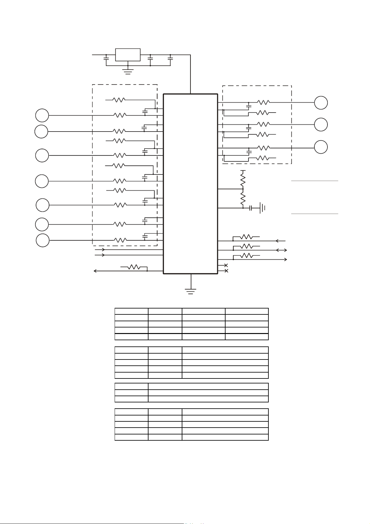
Figure 1.1 Connection Diagram - Full Options (32-QFN Package)
KEY 3
KEY 4
KEY 5
KEY 6
KEY 7
KEY 8
KEY 9
Vunreg
RESET IN
SYNC or LP
DETECT OUT
Voltage Reg
Keep these parts
close to the IC
MOD_1
V / V
DD SS
1M
R
SNS3
R
SNS4
OUT_D
V / V
DD SS
1M
R
SNS5
SL_0
V / V
DD SS
1M
R
SNS6
SL_1
V / V
DD SS
1M
SNS7
R
R
SNS8
R
SNS9
Pull-up not required for push-pull mode
See Detect pin mode table
Vdd
100K
C
S3
C
S4
C
S5
C
S6
C
S7
C
S8
C
S9
*100nF
12
SNS3
13
SNS3K
14
SNS4
15
SNS4K
16
SNS5
17
SNS5K
18
SNS6
19
SNS6K
20
21
25
26
27
SNS9
28
2
23
SYNC/LP
24
DETECT
SNS7
SNS7K
SNS8
SNS8K
SNS9K
/RST
VDD
*Note: One bypass capacitor to be tightly wired between
Vdd and Vss. Follow regulator manufacturer’s
recommendations for input and output capacitors.
11
10
9
8
7
6
4
1
32
31
30
29
5
Keep these parts
close to the IC
C
S2
1M
C
S1
1M
C
S0
1M
VDD
Rb1
Rb2
Css
100K
100K
100K
Vdd
Vdd
Vdd
3
VDD
QT1103
32-QFN
VSS
22
SNS2K
SNS2
SNS1K
SNS1
SNS0K
SNS0
OSC
SS
RX
1W
/CHANGE
N.C.
N.C.
R
R
R
SNS2
SNS1
SNS0
MOD_0
VV
DD SS
/
AKS_1
VV
DD SS
/
AKS_0
VV
DD SS
/
Recommended Rb1, Rb2 Value
With Spread-Spectrum
Vdd Range Rb1 Rb2
2.8 ~ 2.99V 12K 27K
3.0 ~ 3.59V 12K 22K
3.6 ~ 5V 15K 27K
No Spread-Spectrum
Vdd Range Rb1 Rb2
2.8 ~ 2.99V 15K dni
3.0 ~ 3.59V 18K dni
3.6 ~ 5V 20K dni
dni = do not install
2W DATA
DATA
/CHANGE
KEY 2
KEY 1
KEY 0
Table 1.2
AKS / Fast-Detect Options
Table 1.3
Max On-Duration
Table 1.4
Detect Pin Drive
Table 1.5
SYNC/LP Function
Lq
FAST-DETECTAKS MODEAKS_0AKS_1
OffOffVssVss
EnabledOffVddVss
OffOn, in 3 groupsVssVdd
OffOn, globalVddVdd
MAX ON-DURATION MODEMOD_0MOD_1
10 seconds to recalibrateVssVss
60 seconds to recalibrateVddVss
Infinite (disabled)VssVdd
(reserved)VddVdd
DETECT PIN MODEOUT_D
Open drain, active lowVss
Push-pull, active highVdd
SYNC/LP PIN MODESL_0SL_1
SyncVssVss
LP mode: 70ms response timeVddVss
LP mode: 110ms response timeVssVdd
LP mode: 190ms response timeVddVdd
6 QT1103_3R0.03_0607
Page 7

Figure 1.2 Connection Diagram - Simplified Mode (32-QFN Package)
KEY 3
KEY 4
KEY 5
KEY 6
KEY 7
KEY 8
KEY 9
Vunreg
RESET IN
LP IN
DETECT OUT
Voltage Reg
Keep these parts
close to the IC
C
S3
R
SNS3
C
S4
R
SNS4
C
R
SNS5
SNS6
SNS7
SNS8
SNS9
S5
C
S6
C
S7
C
S8
C
S9
R
R
R
R
SMR
1M
*100nF
12
13
14
15
16
17
18
19
20
21
25
26
27
28
2
23
24
VDD
SNS3
SNS3K
SNS4
SNS4K
SNS5
SNS5K
SNS6
SNS6K
SNS7
SNS7K
SNS8
SNS8K
SNS9
SNS9K
/RST
SYNC/LP
DETECT
*Note: One bypass capacitor to be tightly wired between
Vdd and Vss. Follow regulator manufacturer’s
recommendations for input and output capacitors.
Keep these parts
11
C
10
9
C
8
7
C
6
close to the IC
R
S2
R
S1
S0
1M
VDD
SNS2
SNS1
R
SNS0
AKS_0
VV
DD SS
/
Recommended Rb1, Rb2 Values
3
VDD
SNS2K
SNS1K
SNS0K
QT1103
SNS2
SNS1
SNS0
32-QFN
Rb1
4
OSC
Rb2
100K
100K
100K
Css
Vdd
Vdd
Vdd
VSS
22
SS
RX
1W
/CHANGE
N.C.
N.C.
1
32
31
30
29
5
KEY 2
KEY 1
KEY 0
With Spread-Spectrum
Vdd Range Rb1 Rb2
2.8 ~ 2.99V 12K 27K
3.0 ~ 3.59V 12K 22K
3.6 ~ 5V 15K 27K
No Spread-Spectrum
Vdd Range Rb1 Rb2
2.8 ~ 2.99V 15K dni
3.0 ~ 3.59V 18K dni
3.6 ~ 5V 20K dni
dni = do not install
2W DATA
DATA
/CHANGE
Table 1.6
AKS Resistor Options
FAST-DETECTAKS MODEAKS_0
EnabledOffVss
OffOn, globalVdd
Table 1.7
Functions in Simplified
Mode
SYNC/LP pin
Max on-duration delay
Detect Pin
Suggested regulator manufacturers:
• Toko (XC6215 series)
• Seiko (S817 series)
• BCDSemi (AP2121 series)
Re Figures 1.1 and 1.2 check the following sections for the variable component values:
• Section 3.3, page 12: Cs capacitors (C
• Section 3.4, page 12: Sample resistors (R
S
)
SNS
)
• Section 3.5, page 12: Voltage levels
• Section 3.2, page 12: Css capacitor
Lq
110ms LP function; sync not available
60 seconds
Push-pull, active high
7 QT1103_3R0.03_0607
Page 8

2 Device Operation
2.1 Reset and Startup Time
After a reset event, the device typically requires 260ms to
initialize, calibrate, and start operating normally. Keys will
work properly once all keys have been calibrated after reset.
The QT1103 does not have a brownout detector; its reset
input must be taken active (low) following power-up and when
Vdd falls below 2V.
2.2 Option Resistors
The option resistors are read on power-up only. There are
two primary option mode configurations: full, and simplified.
Full options mode: Seven 1M option resistors are required
as shown in Figure 1.1. All seven resistors are mandatory.
Simplified mode: A 1M resistor should be connected from
SNS6K to SNS7. In simplified mode, only one additional 1M
option resistor is required for the AKS feature (Figure 1.2).
Note that the presence and connection of option resistors will
influence the required values of Cs; this effect will be
especially noticeable if the Cs values are under 22nF. Cs
values should be adjusted for optimal sensitivity after the
option resistors are connected.
2.3 DETECT Pin
DETECT represents the functional logical-OR of all ten keys.
DETECT can be used to wake a battery-operated product
upon human touch.
The output polarity and drive of DETECT are governed
according to Table 1.4, page 6, and Table 1.7, page 7.
2.4 /CHANGE Pin
The /CHANGE pin can be used to tell the host that a change
in touch state has been detected (i.e. a key has been
touched or released), and that the host should read the new
key states over the serial interface. /CHANGE is pulled low
when a key state change has occurred.
/CHANGE is very useful to prevent transmissions with
duplicate data. If /CHANGE is not used, the host would need
to keep polling the QT1103 constantly, even if there are no
changes in touch. Upon detection of a key, /CHANGE will pull
low and stay low until the serial interface has been polled by
the host. /CHANGE will then be released and return high until
the next change of key state, either on or off, on any key
(Figures 2.6, 2.9).
The /CHANGE pin is open-drain, and requires a ~100k
pull-up resistor to Vdd in order to function properly.
2.5 SYNC/LP Pin
2.5.1 Introduction
The SYNC / LP pin function is configured according to the
SL_0 and SL_1 resistor connections to either Vdd or Vss
(see Table 1.5).
2.5.2 Sync Mode
Sync mode allows the designer to synchronize acquire bursts
to an external signal source, such as mains frequency
(50/60Hz), to suppress interference. It can also be used to
synchronize two QT parts which operate near each other, so
that they will not cross-interfere if two or more of the keys (or
associated wiring) of the two parts are near each other.
The SYNC input is positive pulse triggered. Following each
rising edge the device will generate three acquire bursts in
C-A-B sequence.
Figure 2.1 Acquire Bursts in C-A-B Sequence
SYNC
Burst C
Burst A
Burst B
If the SYNC input does not change level for ~150ms, the
QT1103 will free-run, generating a continuous stream of
acquire bursts C-A-B-C-A-B-C-A-... . While the QT1103 is in
free-run operation, a rising edge on the SYNC input will
return the QT1103 to synchronised operation.
Note that the SYNC input must remain at one level (high or
low) for >150µs to guarantee that the QT1103 will recognise
that level.
2.5.3 Low Power (LP) Mode
LP mode allows the device to be switched between full speed
operation (14ms (normal mode) or 28ms (fast mode) typical
response time and normal power consumption), and Low
Power operation (low average power consumption but an
increased maximum response time) according to the needs
of the application. There are three maximum response time
settings for low power operation: 70ms, 110ms, and 190ms
nominal;
resistors SL_1 and SL_0 (see Table 1.5). Slower response
times result in a lower average power drain.
Operation in low power mode is governed by the state of the
LP input and whether at least one key has a confirmed touch.
If the LP input is at a constant low level, then the QT1103 will
remain in full speed operation (14ms or 28ms typical
response time and normal power consumption), as in
Figure 2.2.
the response time setting is determined by option
Figure 2.2 Full Speed Operation
touch
LP pin
bursts
full speed operation
Lq
8 QT1103_3R0.03_0607
Page 9

If the LP input is at a constant high level, then the QT1103
will enter low power operation whenever it is not detecting a
touch. It will switch automatically to full speed operation while
there is a touch, and revert to low power operation at the end
of the touch. This is shown in Figure 2.3.
Figure 2.3 Low Power/Full Speed Operation
touch
e
If this is done the QT1103 automatically selects an optimized
LP operation, which gives a significantly lower power
consumption than would be achieved if additional acquire
bursts were used.
Optimized LP operation is identical to the standard LP
operation in all other ways; it is controlled as described
previously.
LP pin
bursts
full speed low power low power
While there is no touch, if the LP input is driven high then
low, the QT1103 will enter low power operation, as described
previously, and remain in low power operation when LP is
taken low. When there is a touch the QT1103 will switch
automatically to full speed operation. At the end of the touch
the choice of operation depends on the state of the LP input.
This is shown in Figures 2.4 and 2.5 - the first with the LP pin
being low at the end of the touch, and the second with the LP
pin being high at the end of the touch.
Figure 2.4 LP Pin Low at End of Touch
touch
e
LP pin
bursts
low power
Figure 2.5 LP Pin High at End of Touch
touch
e
full speed
2.6 AKS™ Function Pins
The QT1103 features an adjacent key suppression (AKS™)
function with two modes. Option resistors act to set this
feature according to Tables 1.2 and 1.6. AKS can be
disabled, allowing any combination of keys to become active
at the same time. When operating, the modes are:
Global: The AKS function operates across all ten keys. This
means that only one key can be active at any one time.
Groups: The AKS function operates among three groups of
keys: 0-1-4-5, 2-3-6-7, and 8-9. This means that up to three
keys can be active at any one time.
In Group mode, keys in one group have no AKS interaction
with keys in any other group.
Note that in Fast Detect mode, AKS can only be off.
2.7 MOD_0, MOD_1 Inputs
In full option mode, the MOD_0 and MOD_1 resistors are
used to set the 'Max On-Duration' recalibration timeouts. If a
key becomes stuck on for a lengthy duration of time, this
feature will cause an automatic recalibration event of that
specific key only once the specified on-time has been
exceeded. Settings of 10s, 60s, and infinite are available.
The Max On-Duration feature operates on a key-by-key
basis; when one key is stuck on, its recalibration has no
effect on other keys.
The logic combination on the MOD option pins sets the
timeout delay; see Table 1.3.
Simplified mode MOD timing: In simplified mode, the max
on-duration is fixed at 60s.
LP pin
bursts
full speed low power low power
Note that the LP input must remain at one level (high or low)
for >150µs to guarantee that the QT1103 will recognise that
level.
Optimization of LP Mode
For low power consumption, when up to eight keys are
required, all keys should be connected to QT1103 channels
that are measured during acquire bursts A and B
(i.e. K0...K7).
For the lowest possible power consumption, when up to four
keys are required, all keys should be connected to QT1103
channels that are measured during acquire burst B (i.e. K2,
K3, K6, K7).
Lq
2.8 Fast Detect Mode
In many applications, it is desirable to sense touch at high
speed. Examples include scrolling ‘slider’ strips or ‘Off’
buttons. It is possible to place the device into a ‘Fast Detect’
mode that usually requires under 14ms (typical) to respond.
This is accomplished internally by setting the Detect
Integrator to only three counts, i.e. only three successive
detections are required to detect touch.
In LP mode, ‘Fast’ detection will not speed up the initial delay
(which could be up to 190ms typical depending on the option
setting). However, once a key is detected the device is forced
back into normal speed mode. It will remain in this faster
mode until requested to return to LP mode.
When used in a ‘slider’ application, it is normally desirable to
run the keys without AKS.
In Fast mode the time required to process a key release is
reduced from three samples to two. Fast Detect mode can be
enabled as shown in Tables 1.2 and 1.6.
9 QT1103_3R0.03_0607
Page 10

2.9 Simplified Mode
y
A simplified operating mode which does not require the
majority of option resistors is available. This mode is set by
connecting a resistor labeled SMR between pins SNS6K and
SNS7 (see Figure 1.2).
In this mode there is only one option available - AKS enable
or disable. When AKS is disabled, Fast Detect mode is
enabled; when AKS is enabled, Fast Detect mode is off.
AKS in this mode is global only (i.e. operates across all
functioning keys).
The other option features are fixed as follows:
DETECT Pin: Push-pull, active high
SYNC/LP Function: LP mode, ~110ms response time
Max On-Duration: 60 seconds
See also Tables 1.6 and 1.7.
2.10 Unused Keys
Unused keys should be disabled by removing the
corresponding Cs and Rsns components and connecting
SNS pins as shown in the ‘Unused’ column of Table 1.1.
Unused keys are ignored and do not factor into the AKS
function (Section 2.6).
2.11 Serial 1W Interface
2.11.1 Introduction
The 1W serial interface is an RS-232 based auto baud rate
serial asynchronous interface that requires only one wire
between the host MCU and the QT1103. The serial data are
extremely short and simple to interpret.
Auto baud rate detection takes place by having the host
device send a specific character to the QT1103, which allows
the QT1103 to set its baud rate to match that of the host.
One feature of this method is that the baud rate can be any
rate between 8,000 and 38,400 bits per second. Neither the
QT1103 nor the host device has to be accurate in their
transmission rates, i.e. crystal control is not required.
Figure 2.6 Basic 1W Sequence
driven repl
from QT1103
(2 bytes)*
1 ~ 3 bit periods
1W
/CHANGE
1W
(from host)
request
key state
change
floating floating
floating floating
from host
(1 byte)
Figure 2.7 1W UART Host Pattern
Depending on the timing of a 1W host transmission, the
QT1103 device may need to abort an acquisition burst, and
rerun it after the transmission is complete and a reply has
been sent. As a consequence, each host request can
potentially result in a small, unnoticeable increase in
detection delay.
1W Connection: The 1W pin should be pulled high with a
resistor. When not in use it floats high, hence this causes no
increase in supply current.
During transmission from the host, the host may drive the 1W
line with either an open-drain or a push-pull driver. However,
if the host uses push-pull driving, it must release the 1W line
as soon as it is done with its stop bit so that there is no drive
conflict when the QT1103 sends its reply.
If open-drain transmission is used by the host, the value of
the pull-up resistor should be optimized for the desired baud
rate: faster rates require a lower value of resistor to prevent
rise-time problems. A typical value for 19,200 baud might be
100k. An oscilloscope should be used to confirm that the
resistor is not causing excessive timing skew that might
cause bit errors.
The QT1103 uses push-pull drive to transmit data out on the
1W line back to the host. When the stop bit level is
established, 1W is floated; for this reason, a pull-up resistor
should always be used on the 1W pin to prevent the signal
from drifting to an undefined state. A 100k pull-up resistor
on 1W is recommended, unless the host uses open-drain
drive to the QT1103, in which case a lower value may be
required (see prior paragraph).
2.11.2 Basic 1W Operation
The basic sequence of 1W serial operation is shown in
Figure 2.6. The 1W line is bi-directional and must be pulled
high with a resistor to prevent a floating, undefined state (see
Section 2.11.1).
Oscillator Tolerance: While the auto baud rate detection
mechanism has a wide tolerance for oscillator error, the QT’s
oscillator should still not vary by more than
the recommended value. Beyond a
communications at either the lower or upper stated limits
could fail. The oscillator frequency can be checked with an
oscilloscope by probing the pulse width on the SNS lines
(see Section 3.1, page 11).
Host Request Byte: The host requests the key
state from the QT1103 by sending an ASCII "P"
character (ASCII decimal code 80, hex 0x50)
over the 1W line. The character is formatted
according to conventional RS-232:
8 data bits
no parity
1 stop bit
baud rate: 8,000 - 38,400
Figure 2.7 shows the bit pattern of the host
*See Figure 2.8
request byte (‘P’). The first bit labeled ‘S’ is the
start bit, the last ‘S’ is the stop bit. This bit pattern
should never be changed. The QT1103 will
respond at the same baud rate as the received
‘P’ character.
±
20 percent from
±
20 percent error,
Serial bits
Lq
S01234 7S
56
10 QT1103_3R0.03_0607
Page 11

After sending the ‘P’ character
y
Figure 2.8 UART Response Pattern on 1W Pin
the host must immediately
float the 1W signal to prevent
a drive conflict between the
host and the QT1103 (see
1W
(from QT1103)
floating
Figure 2.6). The delay from
the received stop bit to the
Serial bits
S01234567 S01234567S
QT1103 driving the 1W pin is
in the range 1-3 bit periods,
so the host should float the
Associated key #
012345
pin within one bit period to
prevent a drive conflict.
Data Reply: Before sending a
reply, the QT1103 returns the /CHANGE signal to its inactive
(float-high) state.
The QT1103 then replies by sending two eight-bit characters
to the host over the 1W line using the same baud rate as the
request. With no keys pressed, both reply bytes are ASCII
‘@’ (0x40) characters; any keys that are pressed at the time
of the reply result in their associated bits being set in the
reply. Figure 2.8 shows the reply bytes when keys 0, 2 and 7
are pressed - 0x45, 0x42, and the associations between keys
and bits in the reply.
The QT1103 floats the 1W pin again after establishing the
level of the stop bit.
2.11.3 LP Mode Effects on 1W
The use of low power (LP) mode presents some additional
1W timing requirements. In LP mode (Section 2.5), the
QT1103 will only respond to a request from the host when it
is making one of its infrequent checks for a key press. Hence,
in that condition most requests from the host to the QT1103
will be ignored, since the QT1103 will be sleeping and
unresponsive. However, if either /CHANGE or DETECT are
active the QT1103 will be at full speed, and hence will always
respond to ‘P’ requests.
Note that when sleeping in LP mode, there are by definition
no keys active, so there should not be a reason for the host
to send the ‘P’ query command in the first place.
Three strategies are available to the host to ensure that LP
mode operates correctly:
• /CHANGE used. The host monitors /CHANGE, and
only sends a ‘P’ request when it is low. The part is
awake by definition when /CHANGE is low. If
/CHANGE is high, key states are known to be
unchanged since the last reply received from the
QT1103, and so additional ‘P’ requests are not
needed. Before triggering LP mode the host should
wait for /CHANGE to go high after all keys have
become inactive.
• DETECT used. The host
monitors DETECT, and if it is
active (i.e. the part is awake) it
polls the device regularly to
obtain key status. When
DETECT is inactive (the part
may be sleeping) no requests
are sent because it is known
that no keys are active. Before
triggering LP mode the host
should wait for DETECT to
become inactive, and then
send one additional 'P' request
to ensure /CHANGE is also
made inactive.
RX
(from host)
1W
(from QT1103)
/CHANGE
floating floating
floating
floating
S
(shown with keys 0, 2 and 7 detecting)
**
• Neither /CHANGE nor DETECT used. The host polls
the device regularly to obtain key status, with a
timeout in operation when awaiting the reply to each
‘P’ request. Not receiving a reply within the timeout
period only occurs when the part is sleeping, and
hence when no keys are active. Before triggering LP
mode the host should wait for all keys to become
inactive and then send an additional 'P' request to the
QT1103 to ensure /CHANGE is also inactive.
2.11.4 2W Operation
1W operation, as described in Section 2.11.3, requires that
the host float the 1W line while awaiting a reply from the
QT1103; this is not always possible.
To solve this problem, the QT1103 can also receive the ‘P’
character from the host on its ‘Rx’ pin separately from the 1W
pin (Figure 2.9). The host need not float the Rx line since the
QT1103 will never try to drive it.
Following a ‘P’ on Rx, the QT1103 will send the same
response pattern (Figure 2.8) over the 1W line as in pure 1W
mode.
All other comments and timings given for 1W operation are
applicable for 2W operation. LP operation is the same for 2W
mode as for 1W.
If the Rx pin is not used, it must be tied to Vdd.
6789UU
**
* Fixed bit values
U - Unused bits
3 Design Notes
3.1 Oscillator Frequency
The QT1103’s internal oscillator runs from an external
network connected to the OSC and SS pins as shown in
Figures 1.1 and 1.2. The charts in these figures show the
recommended values to use depending on nominal operating
voltage and spread spectrum mode.
If spread spectrum mode is not used, only resistor Rb1
should be used, the Css capacitor eliminated, and the SS pin
pulled to Vss with a 100k resistor.
Figure 2.9 2W Operation
key state
change
request
from host
(1 byte)
floating floating
driven repl
(from QT1103)
(2 bytes)
1 ~ 3 bit periods
Lq
11 QT1103_3R0.03_0607
Page 12

An out-of-spec oscillator can induce timing problems such as
large variations in Max On-Duration times and response
times as well as the serial port baud rate range.
Effect on serial communications: The oscillator frequency
has no nominal effect on serial communications since the
baud rate is set by an auto-sensing mechanism. However, if
the oscillator is too far outside the recommended settings,
the possible range of serial communications will shrink. For
example, if the oscillator is too slow, the upper baud rate will
be reduced.
The oscillator frequency can be verified by measuring the
burst pulses at the start of a burst.
• In spread-spectrum mode, the first pulses of a burst
should ideally be 2.87µs
• In non spread-spectrum mode, the target value is
2.67µs
If in doubt, make the pulses on the narrower side (i.e. a faster
oscillator) when using the higher baud rates, and conversely
on the wider side when using the lowest baud rates.
3.2 Spread-spectrum Circuit
The QT1103 offers the ability to spectrally spread its
frequency of operation to heavily reduce susceptibility to
external noise sources and to limit RF emissions. The SS pin
is used to modulate an external passive RC network that
modulates the OSC pin. OSC is the main oscillator current
input. The circuits and recommended values are shown in
Figures 1.1 and 1.2.
The resistors Rb1 and Rb2 should be changed depending on
Vdd. As shown in Figures 1.1 and 1.2, three sets of values
are recommended for these resistors depending on Vdd. The
power curves in Section 4.6 also show the effect of these
resistors.
The circuit can be eliminated, if it is not desired, by using a
resistor from OSC to V
connecting SS to V ss with a 100kΩ resistor (see Section 3.1).
The spread-spectrum RC network might need to be modified
slightly with longer burst lengths. The sawtooth waveform
observed on SS should reach a crest height as follows:
• Vdd >= 3.6V: 17 percent of Vdd
• Vdd < 3.6V: 20 percent of Vdd
The Css capacitor connected to SS (Figures 1.1 and 1.2)
should be adjusted so that the waveform approximates the
above amplitude, ±10 percent, during normal operation in the
target circuit. Where the bursts are of differing lengths, the
adjustment should be done for the longer burst. If this is
done, the circuit will give a spectral modulation of 12-15
percent. A typical value of Css is 100nF.
DD
to drive the oscillator, and
3.3 Cs Sample Capacitors - Sensitivity
The Cs sample capacitors accumulate the charge from the
key electrodes and hence determine sensitivity. The values
of Cs can differ for each channel, permitting differences in
sensitivity from key to key or to balance unequal sensitivities.
Higher values of Cs make the corresponding key more
sensitive.
Unequal sensitivities can occur due to key size and
placement differences, stray wiring capacitances, and option
resistor connection.
• More stray capacitance on an electrode or sense
trace will decrease sensitivity on the corresponding
key; Cs will have to be increased to compensate.
• An option resistor pulling low will increase sensitivity
on the corresponding key; Cs will have to be reduced
to compensate.
The Cs capacitors can be virtually any plastic film or low to
medium-K ceramic capacitor. Acceptable capacitor types for
most uses include PPS film, polypropylene film, and NP0 and
X5R / X7R ceramics. Lower grades than X5R / X7R are not
advised.
For most applications Cs will be in the range 680pF to 50nF;
larger values of Cs require better quality capacitors to ensure
reliable sensing. In a few applications sufficient sensitivity will
be achieved with Cs less than 680pF.
If very high sensitivity is required then the 50nF value may be
exceeded hence the 100nF maximum in Section 4.2,
page 13; in this case greater care should be taken over the
QT1103 circuit layout and interactions with neighboring
electronics.
As the sensitivity of the keys, and hence the required values
of Cs, are affected by the presence and connection of the
option resistors (see Section 2.2, page 9), then final selection
of Cs values should take place after the options choice has
been finalized.
3.4 Rsns Resistors
Series resistors R
electrode connections and should be used to limit
electrostatic discharge (ESD) currents and to suppress radio
frequency interference (RFI). For most applications R
be in the range 4.7k to 33k each. In a few applications
with low loading on the sense keys the value may be up to
100k.
Although these resistors may be omitted, the device may
become susceptible to external noise or RFI. For details of
how to select these resistors see the Application Note
AN-KD02, downloadable from the Quantum website
http://www.qprox.com
Application Notes).
SNS
(R
SNS
0...R
SNS
9) are in line with the
(go to the Support tab and click
SNS
will
3.5 Power Supply
The power supply can range from 2.8V to 5.0V. If this
fluctuates slowly with temperature, the device will track and
compensate for these changes automatically with only minor
changes in sensitivity. If the supply voltage drifts or shifts
quickly, the drift compensation mechanism will not be able to
keep up, causing sensitivity anomalies or false detections.
The power supply should be locally regulated using a
three-terminal device, to between 2.8V and 5.0V. If the
supply is shared with another electronic system, care should
be taken to ensure that the supply is free of digital spikes,
sags, and surges which can cause adverse effects. It is not
recommended to include a series inductor in the power
supply to the QT1103.
For proper operation a 0.1µF or greater bypass capacitor
must be used between Vdd and Vss. The bypass capacitor
should be routed with very short tracks to the device’s Vss
and Vdd pins.
3.6 PCB Layout and Construction
Refer to Quantum application note AN-KD02 for information
related to layout and construction matters.
Lq
12 QT1103_3R0.03_0607
Page 13

4 Specifications
p
@
4.1 Absolute Maximum Specifications
Operating temperature, Ta............................................................................. -40o ~ +85oC
Storage temp, Ts.................................................................................... -50
Vdd..................................................................................................-0.3 ~ +6.0V
Max continuous pin current, any control or drive pin............................................................ ±20mA
Short circuit duration to ground or Vdd, any pin.................................................................infinite
Voltage forced onto any pin..................................................................-0.3V ~ (Vdd + 0.3) Volts
4.2 Recommended Operating Conditions
Operating temperature, Ta............................................................................. -40o ~ +85oC
V
DD
................................................................................................. +2.8 ~ +5.0V
Short-term supply ripple+noise.............................................................................. ±5mV/s
Long-term supply stability.................................................................................. ±100mV
Cs range................................................................................................. [100nF
Cx range................................................................................................ 0 ~ 50pF
4.3 AC Specifications
Vdd = 5.0V, Ta = recommended, Cx = 5pF, Cs = 4.7nF; circuit of Figure 1.1
NotesUnitsMaxTypMinDescriptionParameter
Recalibration timeTrc
Burst center frequencyFc
Burst modulation, percentFm
Sample pulse durationTpc
Startup time from cold startTsu
Burst durationTbd
Response time - Fast modeTdtf
Response time - Normal modeTdtn
Response time - LP modeTdtl
Release time - Fast modeTdrf
Release time - Normal modeTdrn
150
132
15
2
260
2.5
14
28
110
10
14
ms
kHz
ms
ms
ms
baud38,4008,000Serial communications speedbps
Total deviation%
Pulses appear 33 percent longer
µs
when viewed on an oscillosco
All three bursts ms
110ms LP settingms
End of touchms
End of touchms
µs1External reset low pulse widthTres
o
~ +125oC
e.
4.4 DC Specifications
Vdd = 5.0V, Ta = recommended, Cx = 5pF, Cs = 4.7nF, Ta = recommended range; circuit of Figure 1.1 unless noted
NotesUnitsMaxTypMinDescriptionParameter
Iddn
Iddl
*No spread spectrum circuit
Average supply current,
normal mode*
Average supply current,
LP mode*
Average supply current, LP
mode
Average supply current, LP
mode, keys on bursts A and B
only
Average supply current,
LP mode, keys on burst B only
22
15
48
34
36
24
20
14
2.5
1.8
1.4
mA84.2
µA
µA
µA
µA
V/s100Average supply turn-on slopeVdds
V0.7Low input logic levelVil
V3.5High input logic levelVhl
µA±1Input leakage currentIil
bits8Acquisition resolutionAr
DD
= 5.0
@ V
@ V
DD
= 4.0
DD
= 3.3
@ V
VDD = 2.8
@ V
DD
= 3.3V; 190ms LP mode
DD
= 2.8V; 190ms LP mode
@ V
DD
= 3.3V
@ V
DD
= 2.8V
@ V
DD
= 3.3V
@ V
DD
= 2.8V
@ V
@ V
DD
= 3.3V
@ VDD = 2.8V
7mA sinkV0.5Low output voltageVol
2.5mA sourceVVdd-0.5High output voltageVoh
Lq
13 QT1103_3R0.03_0607
Page 14

4.5 Signal Processing
Vdd = 5.0V, Ta = recommended, Cx = 5pF, Cs = 4.7nF, 2µs QT Pulses
NotesUnitsValueDescription
Threshold for increase in Cx loadcounts10Detection threshold
counts2Detection hysteresis
Threshold for decrease of Cx loadcounts6Anti-detection threshold
Time to recalibrate if Cx load has exceeded anti-detection thresholdsecs2Anti-detection recalibration delay
Must be consecutive or detection failssamples6Detect Integrator filter, normal mode
Must be consecutive or detection failssamples3Detect Integrator filter, Fast mode
Option pin selectedsecs10, 60, infMax On-Duration
Towards increasing Cx loadms/level2,000Normal drift compensation rate
Towards decreasing Cx loadms/level500Anti drift compensation rate
Lq
14 QT1103_3R0.03_0607
Page 15

4.6 Idd Curves
All Idd curves are average values, under the following conditions: Cx = 5pF, Cs = 4.7nF, Ta = 20oC; no spread-spectrum
circuit. Refer to page 9 for more information about optimization of LP modes.
QT1103, average Idd (full speed operation)
5.0
4.0
3.0
2.0
Idd (mA)
1.0
0.0
0123456
burst length (ms)
Full speed operation
Low Power operation (optimized - only burst B in use)
QT1103, average Idd (70ms optimized LP operation)
1500.0
Vdd=5V
Vdd=4V
Vdd=3.3V
Vdd=2.8V
QT1103, average Idd (110ms optimized LP
1000.0
operation)
1250.0
1000.0
750.0
Idd (uA)
500.0
250.0
0.0
0123456
burst length (ms)
QT1103, average Idd (190ms optimized LP
500.0
400.0
300.0
200.0
Idd (uA)
100.0
0.0
0123456
operation)
burst length (ms)
Vdd=5V
Vdd=4V
Vdd=3.3V
Vdd=2.8V
Vdd=5V
Vdd=4V
Vdd=3.3V
Vdd=2.8V
800.0
600.0
400.0
Idd (uA)
200.0
0.0
0123456
burst length (ms)
Vdd=5V
Vdd=4V
Vdd=3.3V
Vdd=2.8V
lQ 15 QT1103_3R0.03_0607
Page 16

Low Power operation (optimized - only burst A and B in use)
QT1103, average Idd (70ms optimized LP operation)
1500.0
QT1103, average Idd (110ms optimized LP
1000.0
operation)
1250.0
1000.0
750.0
Idd (uA)
500.0
250.0
0.0
0123456
burst length (ms)
QT1103, average Idd (190ms optimized LP
500.0
400.0
300.0
200.0
Idd (uA)
100.0
0.0
0123456
operation)
burst length (ms)
Vdd=5V
Vdd=4V
Vdd=3.3V
Vdd=2.8V
Vdd=5V
Vdd=4V
Vdd=3.3V
Vdd=2.8V
800.0
600.0
400.0
Idd (uA)
200.0
0.0
0123456
burst length (ms)
Vdd=5V
Vdd=4V
Vdd=3.3V
Vdd=2.8V
lQ 16 QT1103_3R0.03_0607
Page 17

Low Power operation (non-optimized)
QT1103, average Idd (70ms LP operation)
1500.0
1250.0
1000.0
750.0
Idd (uA)
500.0
250.0
0.0
0123456
burst length (ms)
QT1103, average Idd (190ms LP operation)
500.0
400.0
300.0
200.0
Idd (uA)
100.0
Vdd=5V
Vdd=4V
Vdd=3.3V
Vdd=2.8V
Vdd=5V
Vdd=4V
Vdd=3.3V
Vdd=2.8V
QT1103, average Idd (110ms LP operation)
1000.0
800.0
600.0
400.0
Idd (uA)
200.0
0.0
0123456
burst length (ms)
Vdd=5V
Vdd=4V
Vdd=3.3V
Vdd=2.8V
0.0
0123456
burst length (ms)
lQ 17 QT1103_3R0.03_0607
Page 18

4.7 LP Mode Typical Response Times
90
85
80
75
70
Response Time, ms
65
60
Response Time vs Vdd - 70ms Setting
2.533.544.555.5
Vdd
Response Time vs Vdd - 190ms Setting
240
230
220
210
200
190
180
170
Response Time, ms
160
150
2.50 3.00 3.50 4.00 4.50 5.00 5.50
Response Time vs Vdd - 110ms Setting
140
130
120
110
100
Response Time, ms
90
80
2.50 3.00 3.50 4.00 4.50 5.00 5.50
Vdd
Vdd
lQ 18 QT1103_3R0.03_0607
Page 19

4.8 Mechanical Dimensions
DimensionsIn Millimeters
Symbol Minim um Nominal Maximum
A 0.70 - 0.95
A1 0.00 0.02 0.05
b 0.18 0.25 0.32
C-0.20REFD 4.90 5.00 5.10
D2 3.05 - 3.65
E 4.90 5.00 5.10
E2 3.05 - 3.65
e-0.50L 0.30 0.40 0.50
y0.00-0.075
Note: that there is no functional requirement for the large pad on the underside of the 32-QFN
package to be soldered to the substrate. If the final application does require this area to be soldered
for mechanical reasons, the pad(s) to which it is soldered to must be isolated and contained under the
32-QFN footprint only.
Lq
19 QT1103_3R0.03_0607
Page 20

4.9 Part Marking
QT1103
©QRG 3
YYWWG
run nr.
QRG Part
Number
QRG Revision
Code
‘YY’ = Year of manufacture
‘WW’ = Week of manufacture
‘G’ = Green/RoHS Compliant
Pin 1
Identification
4.10 Moisture Sensitivity Level (MSL)
'run nr.' = 6 Digit Run Number
SpecificationsPeak Body TemperatureMSL Rating
IPC/JEDEC J-STD-020C260OCMSL3
Lq
20 QT1103_3R0.03_0607
Page 21

5 Datasheet Control
5.1 Changes
Changes this issue (datasheet issue 03)
Front page.
5.2 Numbering Convention
Part Number
Datasheet Issue Number
QT1103_MXN.nn_mmyy
Chip Revision
(Where M= Major chip revision,
N = Minor chip revision,
X = Prereleased Product
[or R = Released Product])
A minor chip revision (N) is defined as a revision change which does not affect product functionality or datasheet.
The value of N is only stated for released parts (R).
Datasheet Release Date;
(Where mm = Month, yy = Year)
lQ 21 QT1103_3R0.03_0607
Page 22

LQ Copyright © 2006-2007 QRG Ltd. All rights reserved.
Patented and patents pending
Corporate Headquarters
1 Mitchell Point
Ensign Way, Hamble SO31 4RF
Great Britain
Tel: +44 (0)23 8056 5600 Fax: +44 (0)23 8045 3939
www.qprox.com
North America
651 Holiday Drive Bldg. 5 / 300
Pittsburgh, PA 15220 USA
Tel: 412-391-7367 Fax: 412-291-1015
The specifications set out in this document are subject to change without notice. All products sold and services supplied by QRG are
subject to QRG’s Terms and Conditions of sale and services. QRG patents, trademarks and Terms and Conditions can be found online at
http://www.qprox.com/about/legal.php. Numerous further patents are pending, one or more which may apply to this device or the
applications thereof.
QRG products are not suitable for medical (including lifesaving equipment), safety or mission critical applications or other similar
purposes. Except as expressly set out in QRG's Terms and Conditions, no licenses to patents or other intellectual property of QRG
(express or implied) are granted by QRG in connection with the sale of QRG products or provision of services. QRG will not be liable for
customer product design and customers are entirely responsible for their products and applications which incorporate QRG's products.
Development Team: John Dubery, Alan Bowens, Matthew Trend
 Loading...