

Page 1
lQ QT1100A-ISG
A
DVANCED INFORMATION
z 10 independent touch sensing fields
z 100% autocal for life - no adjustments required
z SPI and UART serial interfaces
z Scanport output - simulates a membrane keypad
z Simple external per channel passive circuit
z User-defined setups of operating parameters
z 3.3V~5.0V single supply operation
z AKS™ Adjacent Key Suppression for tight key layouts
z Sleep mode for low power operation
z Spread spectrum modulated bursts - superior noise rejection
z Sync pin for superior mains frequency noise rejection
z FMEA compliant design features - self detects faults
z Lower per key cost than many mechanical switches
z Lead-free package
10 KEY QT
OUCH
™ S
ENSOR
IC
APPLICATIONS
PC peripherals
Television controls
Instrument panels
QT1100A charge-transfer (“QT”) QTouch ICs are self-contained digital controllers capable of detecting near-proximity or touch on up to
10 electrodes. This device allows each electrode to project an independent sense field through glass or plastic. These devices require
only a few inexpensive passive components per sensing channel. The devices are designed specifically for human interfaces, such as
control panels, appliances, gaming devices, lighting controls, or anywhere a mechanical switch may be found.
Each key channel operates independently, and can be tuned to a unique sensitivity level by simply changing setup values in an
EEPROM or via a serial interface. An external EEPROM can store the setups permanently for standalone applications, for example
when using the scanport, or, the EEPROM can be omitted if the serial port is used to send setup information after each power-up.
Included is patent pending AKS™ Adjacent Key Suppression which suppresses touch from weakly responding keys and allows only a
dominant key to detect, to solve the problem of large fingers on tightly spaced keys. Modulated burst technology provides superior
noise rejection. ‘Fast-DI’ operation works to further suppress false activations due to noise.
These devices also have a Sync pin to suppress some forms of external interference. A Sleep mode is also available for very low
power standby operation.
The QT1100A is designed specifically to assist in creating FMEA compliant designs, allowing it to be used in applications such as
appliance controls.
Using the charge transfer principle, these devices deliver a level of performance which is clearly superior to older technologies yet
extremely cost-effective.
Appliance controls
Pointing devices
Gaming machines
Actual Size
LQ
AVAILABLE OPTIONS
A
1
LEAD-FREESSOP-48T
YesQT1100A-ISG-40ºC to +85ºC
Copyright © 2003-2005 QRG Ltd
QT1100A-ISG R3.02/1105
Page 2

Contents
1 Overview
Table 1.1 Scanport / UART Pinlist
Table 1.2 Standalone Pinlist
Table 1.3 Standalone Pinlist
Table 1.4 SPI Pinlist
Table 1.5 Pin Descriptions
Figure 1.1 SPI Connection Diagram
Figure 1.2 UART / Scanport Connection Diagram
Figure 1.3 Scanport Only Connection Diagram+
2 Device Control & Wiring
2.1 Oscillator
2.2 Spread Spectrum Modulation
2.3 Cs Sample Capacitors
2.4 Sensitivity
2.5 Sensitivity Balance
2.6 Power Supply
2.7 PCB Layout and Construction
2.8 ESD Protection
2.9 Noise Issues
2.10 Start-up Time
2.11 Operating Parameter Setups
2.12 Standalone Operation, No EEPROM
2.13 EEPROM Functionality
2.14 Scanport Interface
2.15 Start-up Sequencing
2.16 Error Detection and Reporting
3 Serial Operation
3.1 UART Interface
3.2 SPI Operation
3.3 Communication Error Handling
3.4 Control Commands
3.5 Status Commands
..............................
..................
.....................
.....................
.........................
......................
.................
....................
............................
..................
......................
............................
.......................
..........................
..................
.........................
2.9.1 LED Traces and Other Switching Signals
2.9.2 External Fields
..........................
........................
.........................
..................
.....................
.......................
......................
.................
.........................
3.1.1 TX Pin
3.1.2 Sleep/Wake Operation in UART Mode
3.1.3 CRDY Operation in UART Mode
3.2.1 Multi-Drop SPI Capability
3.2.2 Sleep/Wake Operation in SPI Mode
3.2.3 CRDY Operation in SPI Mode
.........................
............................
..........................
....................
..................
.................
3.4.1 Null Command - 0x00
3.4.2 Enter Setups Load Mode - 0x01
3.4.3 Enter Run Mode - 0x02
3.4.4 Enter Cal Mode - 0x03
3.4.5 Force Reset - 0x04
3.4.6 Sleep - 0x05
3.4.7 Cal Key ‘k’ - 0x1k
3.5.1 Signal for 1 Key - 0x2k
3.5.2 Reference for Key ‘k’ - 0x4k
.......................
.....................
.................
....................
.....................
......................
.........................
.......................
.......................
.....................
..................
..........
...........
.............
..............
..............
................
...............
3
4
5
6
7
8
9
10
11
12
12
12
12
12
12
12
12
13
13
13
13
13
13
14
14
14
14
14
15
15
15
15
15
16
16
16
16
16
17
17
17
18
18
18
18
19
19
19
19
3.5.3 Detect Integrator for Key ‘k’ - 0x6k
3.5.4 Status for Key ‘k’ - 0x8k
3.5.5 Report 1st Key - 0xC0
3.5.6 Report All Keys - 0xC1
3.5.7 Device Status - 0xC2
3.5.8 EEPROM CRC - 0xC3
3.5.9 RAM CRC - 0xC4
3.5.10 Error Flags for Group - 0xC5
3.5.11 Internal Code - 0xC6
3.5.12 Return Last Command - 0xC7
3.5.13 Dump Setups Block - 0xC8
3.5.14 Quick Report First Key - 0xC9
3.6 Command Sequencing
Figure 3-1 Suggested Serial Flow
Table 3-1 Control Commands
Table 3-2 Status Commands
4 Setup Block Functions
4.1 NTHR - Negative Threshold Bits
4.2 NHYS - Negative Hysteresis Bits
4.3 NDCR / PDCR - Drift Comp Bits
4.4 NRD - Negative Recal Delay Bits
4.5 PRD - Positive Recal Delay Bits
4.6 AKS - Adjacent Key Suppression Bits
4.7 EK - Error Key Control Bits
4.8 K2L / LEDP / KEYO Control Bits
4.9 NDIL, FDIL - Detect Integrator Bits
4.10 PTHR - Positive Threshold Bits
4.11 PHYS - Positive Hysteresis Bits
4.12 SE, SYNC Control Bits
4.13 LBLL - Lower Burst Length Limit
4.14 BS - Burst Spacing Control Bits
4.15 BR - Baud Rate Control Bits
4.16 HCRC - Host CRC
Table 4-1 Serial / EEPROM Setups Block
4.17 Timing Tables
5 - Specifications
5.1 Absolute Maximum Specifications
5.2 Recommended Operating Conditions
5.3 AC Specifications
5.4 DC Specifications
5.5 Burst / Sync Timing
5.6 SPI Timing Diagram
5.7 QT1100A Timing Parameters - with Fosc = 12MHz
5.8 Current vs Vdd
5.9 Mechanical
5.10 Marking
6 Appendix A - 8-Bit CRC C Algorithm
.........................
..........................
........................
........................
.........................
...........................
............................
................
....................
.....................
.....................
.....................
.....................
.......................
.................
.....................
.................
..................
.................
.....................
..................
....................
....................
.....................
.................
................
.................
................
.................
..............
...................
.................
................
.................
................
.....................
................
................
..................
.......................
..............
................
..............
.......................
......................
.......
.............
19
19
20
20
20
20
20
21
21
21
21
21
21
22
23
24
25
25
25
25
26
26
26
27
27
27
28
28
28
29
29
29
30
31
32
36
36
36
36
36
37
38
39
40
40
40
41
LQ
2
Copyright © 2003-2005 QRG Ltd
QT1100A-ISG R3.02/1105
Page 3

1 Overview
The QT1100A is a 10 touch-key sensor IC based on
Quantum’s patented charge-transfer principles for robust
operation and ease of design. This device has many
advanced features which provide for reliable, trouble-free
operation over the life of the product. It can operate in either
a standalone mode or under host control via a serial
interface. Output options include UART and SPI serial types
and parallel scanport. In any interface mode, a low-cost
optional EEPROM can be used to determine the device
configuration using a stored Setup block .
FMEA self-testing: This part has been designed specifically
for demanding appliance applications requiring FMEA
certification. The part has many advanced features that
check for and report failures, to allow the designer to create
a safer product. It also features two robust serial interfaces
with sophisticated CRC error checking to permit validation of
commands and responses in real time.
Burst mode: The device operates in ‘burst mode’. Each key
is acquired using a burst of charge-transfer sensing pulses
whose count can vary tremendously depending on the value
of the reference capacitor Cs and the load capacitance Cx.
The keys (also called ‘channels’) are acquired time
sequentially within fixed timeslots whose width can be
controlled by user-defined Setups.
Self-calibration: On power-up, all keys are self-calibrated
within a few hundred milliseconds to provide reliable
operation under almost any set of conditions.
Auto-recalibration: The device can time out and recalibrate
each key independently after a fixed interval of continuous
detection, so that the keys can never become ‘stuck on’ due
to foreign objects or sudden influences. After recalibration
the key will continue to function normally.
Drift compensation operates to correct the reference level
of each key slowly but automatically over time, to suppress
false detections caused by changes such as temperature,
humidity, dirt and other environmental effects.
Spread Spectrum operation: The bursts operate over a
spread of frequencies, so that external fields will have
minimal effect on key operation and emissions are very
weak. Spread-spectrum operation works with the ‘detect
integrator’ (DI) mechanism to dramatically reduce the
probability of false detection due to noise.
Detection confirmation occurs by means of a ‘detect
integrator’ mechanism that requires multiple confirmations of
detection over a number of key bursts. The bursts operate at
alternating frequencies, so that external fields will have a
minimal effect on key operation. This spread-spectrum
mode of operation also reduces RF noise emissions.
The device also features the ability to acquire and lock onto
touch signals very rapidly, greatly improving response time
through the use of the ‘fast detect integration’ or ‘Fast-DI’
feature.
Sync Mode: The QT1100A features a Sync mode to allow
the device to slave to an external signal source, such as a
mains signal (50/60Hz), to limit interference effects. This is
performed using a special Sync pin.
Low Power Sleep Mode: The device features a low power
Sleep mode for microamp levels of current drain when not in
use. The part can be put into sleep for a certain percentage
of the time, so that it can still respond to touch but with lower
levels of current drain.
AKS™ Adjacent Key Suppression works to prevent
multiple keys responding to a single touch, a common
complaint of capacitive touch panels. This system operates
by comparing signal strengths from keys within a defined
group to suppress touch detections from those with a weaker
signal change than the dominant key. The QT1100A allows
any AKS grouping of two or more keys, under user control.
Unique to this device is the ability for the designer to treat
each key as an individual sensor for configuration purposes.
Each key can be programmed separately for sensitivity, drift
compensation, recalibration timeouts, adjacent key
suppression, and the like.
The device is designed to support FMEA-qualified
applications using a variety of checks and redundancies.
Among other checks the component uses CRC codes in all
critical communication transfers, and can also output error
condition codes via redundant signaling paths.
LQ
3
Copyright © 2003-2005 QRG Ltd
QT1100A-ISG R3.02/1105
Page 4

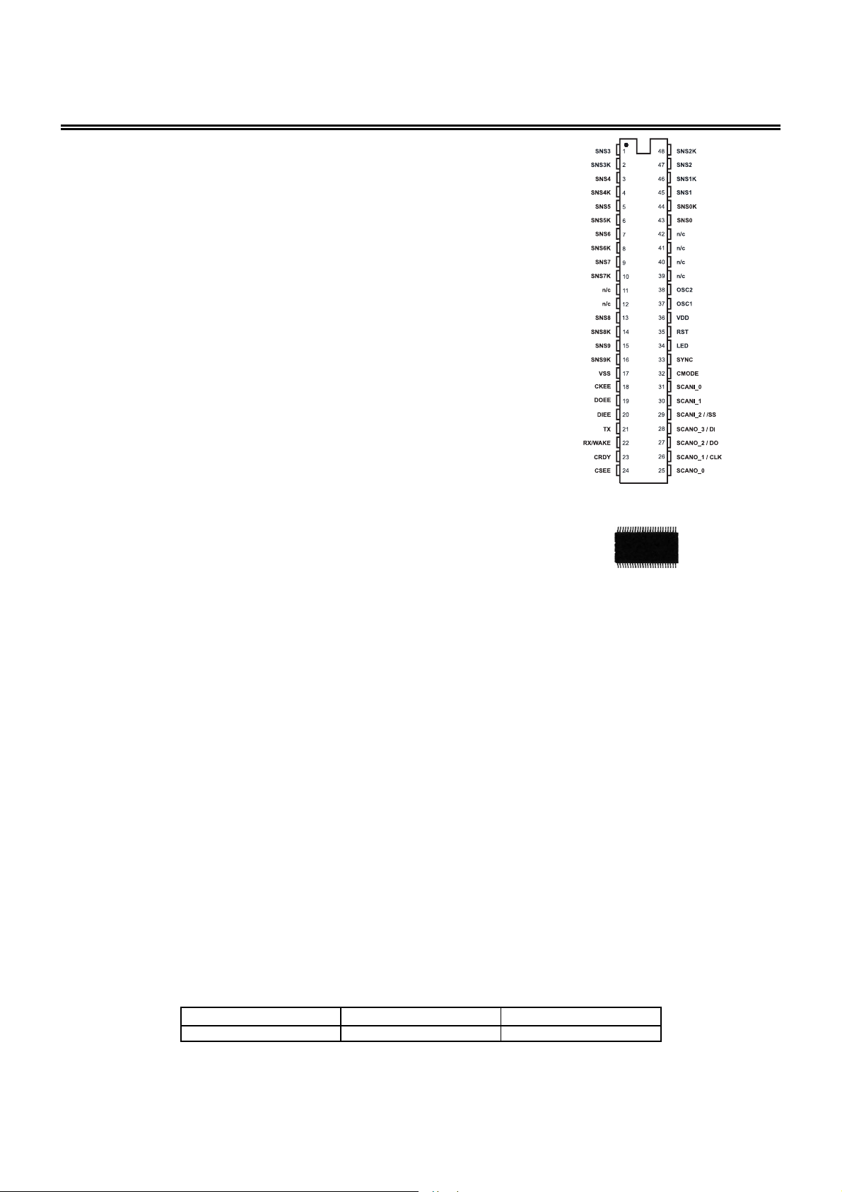
Table 1.1 Scanport / UART Pinlist
With or without EEPROM; either UART or Scanport or both may be used
2
3
4
8
9
10
14
15
16
20
21
22
Sense pinI/OSNS3K
Sense pinI/OSNS4K
Sense pinI/OSNS5K6
Sense pinI/OSNS6K
Sense pinI/OSNS7K
Sense pinI/OSNS8K
Sense pinI/OSNS9K
If UnusedNotesFunctionTypeNamePin
OpenTo CS3Sense pinI/OSNS31
Vss or openTo CS3 + Key
OpenTo CS4Sense pinI/OSNS4
Vss or openTo CS4 + Key
OpenTo CS5Sense pinI/OSNS55
Vss or openTo CS5 + Key
OpenTo CS6Sense pinI/OSNS67
Vss or openTo CS6 + Key
OpenTo CS7Sense pinI/OSNS7
Vss or openTo CS7 + Key
--Unused-n/c11
--Unused-n/c12
OpenTo CS8Sense pinI/OSNS813
Vss or openTo CS8 + Key
OpenTo CS9Sense pinI/OSNS9
Vss or openTo CS9 + Key
-0VGroundPwrVss17
OpenClock to EEPROM EEPROMOCKEE18
OpenData out to EEPROMEEPROMODOEE19
VddData in from EEPROMEEPROMIDIEE
VssSerial to host; If used, use pull-up-R UARTODTX
VddSerial in / Wake from sleepUART, WakeupIRX/WAKE
10K ~ 220K to Vdd1 = Comms ready; use pull-up-RHandshakeI/O, ODCRDY23
OpenEEPROM chip select; use pull-down-REEPROMOCSEE24
OpenSee Table 2.1Scanport outOSCANO_025
26
27
28
32
33
34
38
39
40
44
45
46
OpenSee Table 2.1Scanport outOSCANO_1
OpenSee Table 2.1Scanport outOSCANO_2
OpenSee Table 2.1Scanport outOSCANO_3
VssSee Table 2.1Scanport inISCANI_229
VssSee Table 2.1Scanport inISCANI_130
VssSee Table 2.1Scanport inISCANI_031
-To VssComms selectICMODE
20K ~ 220K to VddAlways use pull-up RSync inI/OSYNC
Open-LED & StatusOLED/STAT
VddActive lowReset inputIRST35
-+3.3 ~ +5VPowerPwrVdd36
-12MHz - Can also be ext clock inResonatorIOSC137
Open-ResonatorOOSC2
--Unused-n/c
--Unused-n/c
--Unused-n/c41
--Unused-n/c42
OpenTo CS0 + KeySense pinI/OSNS043
Vss or openTo CS0Sense pinI/OSNS0K
OpenTo CS1 + KeySense pinI/OSNS1
Vss or openTo CS1Sense pinI/OSNS1K
OpenTo CS2 + KeySense pinI/OSNS247
Vss or openTo CS2Sense pinI/OSNS2K48
I CMOS input
I/O CMOS I/O
O CMOS output (push-pull)
OD CMOS open drain I/O
Pwr Power / ground
LQ
4
Copyright © 2003-2005 QRG Ltd
QT1100A-ISG R3.02/1105
Page 5

Table 1.2 Standalone Pinlist
Scanport, with EEPROM; no serial interface
2
3
4
8
9
10
14
15
16
20
21
22
If UnusedNotesFunctionTypeNamePin
OpenTo CS3Sense pinI/OSNS31
Sense pinI/OSNS3K
Sense pinI/OSNS4K
Sense pinI/OSNS5K6
Sense pinI/OSNS6K
Sense pinI/OSNS7K
Sense pinI/OSNS8K
Sense pinI/OSNS9K
Vss or openTo CS3 + Key
OpenTo CS4Sense pinI/OSNS4
Vss or openTo CS4 + Key
OpenTo CS5Sense pinI/OSNS55
Vss or openTo CS5 + Key
OpenTo CS6Sense pinI/OSNS67
Vss or openTo CS6 + Key
OpenTo CS7Sense pinI/OSNS7
Vss or openTo CS7 + Key
--Unused-n/c11
--Unused-n/c12
OpenTo CS8Sense pinI/OSNS813
Vss or openTo CS8 + Key
OpenTo CS9Sense pinI/OSNS9
Vss or openTo CS9 + Key
-0VGroundPwrVss17
-Clock to EEPROMEEPROMOCKEE18
-Data out to EEPROMEEPROMODOEE19
-Data in from EEPROMEEPROMIDIEE
-To VssUARTODTX
-To VddUART, WakeupIRX/WAKE
-Leave openHandshakeI/O, ODCRDY23
-EEPROM chip selectEEPROMOCSEE24
26
27
28
32
33
34
38
39
40
44
45
46
I CMOS input
I/O CMOS I/O
O CMOS output (push-pull)
OD CMOS open drain I/O
Pwr Power / ground
OpenSee Table 2.1Scanport outOSCANO_025
OpenSee Table 2.1Scanport outOSCANO_1
OpenSee Table 2.1Scanport outOSCANO_2
OpenSee Table 2.1Scanport outOSCANO_3
VssSee Table 2.1Scanport inISCANI_229
VssSee Table 2.1Scanport inISCANI_130
VssSee Table 2.1Scanport inISCANI_031
-To VssComms selectICMODE
20K ~ 220K to VddAlways use pull-up RSync inI/OSYNC
Open-LED & StatusOLED/STAT
VddActive lowReset inputIRST35
-+3.3 ~ +5VPowerPwrVdd36
-12MHz - Can also be ext clock inResonatorIOSC137
Open-ResonatorOOSC2
--Unused-n/c
--Unused-n/c
--Unused-n/c41
--Unused-n/c42
OpenTo CS0 + KeySense pinI/OSNS043
Vss or openTo CS0Sense pinI/OSNS0K
OpenTo CS1 + KeySense pinI/OSNS1
Vss or openTo CS1Sense pinI/OSNS1K
OpenTo CS2 + KeySense pinI/OSNS247
Vss or openTo CS2Sense pinI/OSNS2K48
LQ
5
Copyright © 2003-2005 QRG Ltd
QT1100A-ISG R3.02/1105
Page 6

Table 1.3 Standalone Pinlist
Scanport, without EEPROM; no serial interface
2
3
4
8
9
10
14
15
16
21
Sense pinI/OSNS3K
Sense pinI/OSNS4K
Sense pinI/OSNS5K6
Sense pinI/OSNS6K
Sense pinI/OSNS7K
Sense pinI/OSNS8K
Sense pinI/OSNS9K
EEPROMODOEE19
Connect DOEE, DIEE together
If UnusedNotesFunctionTypeNamePin
OpenTo CS3Sense pinI/OSNS31
Vss or openTo CS3 + Key
OpenTo CS4Sense pinI/OSNS4
Vss or openTo CS4 + Key
OpenTo CS5Sense pinI/OSNS55
Vss or openTo CS5 + Key
OpenTo CS6Sense pinI/OSNS67
Vss or openTo CS6 + Key
OpenTo CS7Sense pinI/OSNS7
Vss or openTo CS7 + Key
--Unused-n/c11
--Unused-n/c12
OpenTo CS8Sense pinI/OSNS813
Vss or openTo CS8 + Key
OpenTo CS9Sense pinI/OSNS9
Vss or openTo CS9 + Key
-0VGroundPwrVss17
-OpenEEPROMOCKEE18
-
-EEPROMIDIEE20
-To VssUARTODTX
-To VddUART, WakeupIRX/WAKE22
-Leave openHandshakeI/O, ODCRDY23
-OpenEEPROMOCSEE24
25
26
27
31
32
33
37
38
39
43
44
45
I CMOS input
I/O CMOS I/O
O CMOS output (push-pull)
OD CMOS open drain I/O
Pwr Power / ground
OpenSee Table 2.1Scanport outOSCANO_0
OpenSee Table 2.1Scanport outOSCANO_1
OpenSee Table 2.1Scanport outOSCANO_2
OpenSee Table 2.1Scanport outOSCANO_328
VssSee Table 2.1Scanport inISCANI_229
VssSee Table 2.1Scanport inISCANI_130
VssSee Table 2.1Scanport inISCANI_0
-To VssComms selectICMODE
20K ~ 220K to VddAlways use pull-up RSync inI/OSYNC
Open-LED & StatusOLED/STAT34
VddActive lowReset inputIRST35
-+3.3 ~ +5VPowerPwrVdd36
-12MHz - Can also be ext clock inResonatorIOSC1
Open-ResonatorOOSC2
--Unused-n/c
--Unused-n/c40
--Unused-n/c41
--Unused-n/c42
OpenTo CS0 + KeySense pinI/OSNS0
Vss or openTo CS0Sense pinI/OSNS0K
OpenTo CS1 + KeySense pinI/OSNS1
Vss or openTo CS1Sense pinI/OSNS1K46
OpenTo CS2 + KeySense pinI/OSNS247
Vss or openTo CS2Sense pinI/OSNS2K48
LQ
6
Copyright © 2003-2005 QRG Ltd
QT1100A-ISG R3.02/1105
Page 7

Table 1.4 SPI Pinlist
With or without EEPROM
1
4
5
8
9
12
13
16
17
20
21
24
If UnusedNotesFunctionTypeNamePin
OpenTo CS3Sense pinI/OSNS3
Vss or openTo CS3 + KeySense pinI/OSNS3K2
OpenTo CS4Sense pinI/OSNS43
Vss or openTo CS4 + KeySense pinI/OSNS4K
OpenTo CS5Sense pinI/OSNS5
Vss or openTo CS5 + KeySense pinI/OSNS5K6
OpenTo CS6Sense pinI/OSNS67
Vss or openTo CS6 + KeySense pinI/OSNS6K
OpenTo CS7Sense pinI/OSNS7
Vss or openTo CS7 + KeySense pinI/OSNS7K10
--Unused-n/c11
--Unused-n/c
OpenTo CS8Sense pinI/OSNS8
Vss or openTo CS8 + KeySense pinI/OSNS8K14
OpenTo CS9Sense pinI/OSNS915
Vss or openTo CS9 + KeySense pinI/OSNS9K
-0VGroundPwrVss
OpenClock to EEPROM EEPROMOCKEE18
OpenData out to EEPROMEEPROMODOEE19
VddData in from EEPROMEEPROMIDIEE
-To VssUnused-n/c
VddWake from sleepWakeIWAKE22
-1 = Comms ready; Use pull-up RSPI handshakeODCRDY23
OpenEEPROM chip select; Use pull-down REEPROMOCSEE
25
28
29
32
33
36
37
40
41
44
45
48
I CMOS input
I/O CMOS I/O
O CMOS output (push-pull)
OD CMOS open drain I/O
Pwr Power / ground
Vss-unusedIn/c
-From hostSPI clockICLK26
-To host; use pull-up RSPI dataI/ODO27
-From hostSPI dataIDI
-From hostSPI Slave selectI/SS
-To VssUnusedIn/c30
-To VssUnusedIn/c31
-To VddComms selectICMODE
20K ~ 220K to VddAlways use pull-up RSync InI/OSYNC
Open -LED & StatusOLED/STAT34
VddActive lowReset inputIRST35
-+3.3 ~ +5VPowerPwrVdd
-12MHz - Can also be ext clock inResonatorIOSC1
Open-ResonatorOOSC238
--Unused-n/c39
--Unused-n/c
--Unused-n/c
--Unused-n/c42
OpenTo CS0 + KeySense pinI/OSNS043
Vss or openTo CS0Sense pinI/OSNS0K
OpenTo CS1 + KeySense pinI/OSNS1
Vss or openTo CS1Sense pinI/OSNS1K46
OpenTo CS2 + KeySense pinI/OSNS247
Vss or openTo CS2Sense pinI/OSNS2K
LQ
7
Copyright © 2003-2005 QRG Ltd
QT1100A-ISG R3.02/1105
Page 8

Table 1.5 Pin Descriptions
DescriptionPin
Sense pin, to Cs reference capacitorSNSn
Sense pin, to Cs and to key electrodeSNSnK
Clock line output, to drive serial EEPROMCKEE
Output data line, to serial EEPROMDOEE
Input data line, from serial EEPROMDIEE
Serial port pin for UARTTX
Receive pin in UART mode; alternately or in addition, Wake from sleep RX/WAKE
CRDY
CMODE
SYNC
LED/STAT
/RST
Serial interface handshake pin; bidirectional in UART mode, output only in SPI
mode. Always use a pull-up resistor on this pin.
Chip select drive to serial EEPROM. Always use a pull-down resistor on this pin.CSEE
SPI clock input from hostCLK
SPI data output to host. Always use a pull-up resistor on this pin.DO
SPI data in from hostDI
SPI Slave select from host/SS
Output scan linesSCANO_x
Input scan linesSCANI_x
Communications mode select pin. For UART or scanport operation, connect to
Vss. For SPI mode, connect to Vdd.
Sync Input to synchronize acquisitions to an external source or another QT chip.
Always use a pull-up resistor on this pin.
LED & Status output pin. This pin can sink 1mA to drive a status LED, or be used
by a host controller to determine device error condition or status .
Reset input, low resets device. Normally this pin can be tied to Vdd, or driven from
a host controller.
Connect to 12MHz resonator; can also be an external clock inputOSC1
Connect to 12MHz resonator; leave open if external clock is usedOSC2
LQ
8
Copyright © 2003-2005 QRG Ltd
QT1100A-ISG R3.02/1105
Page 9
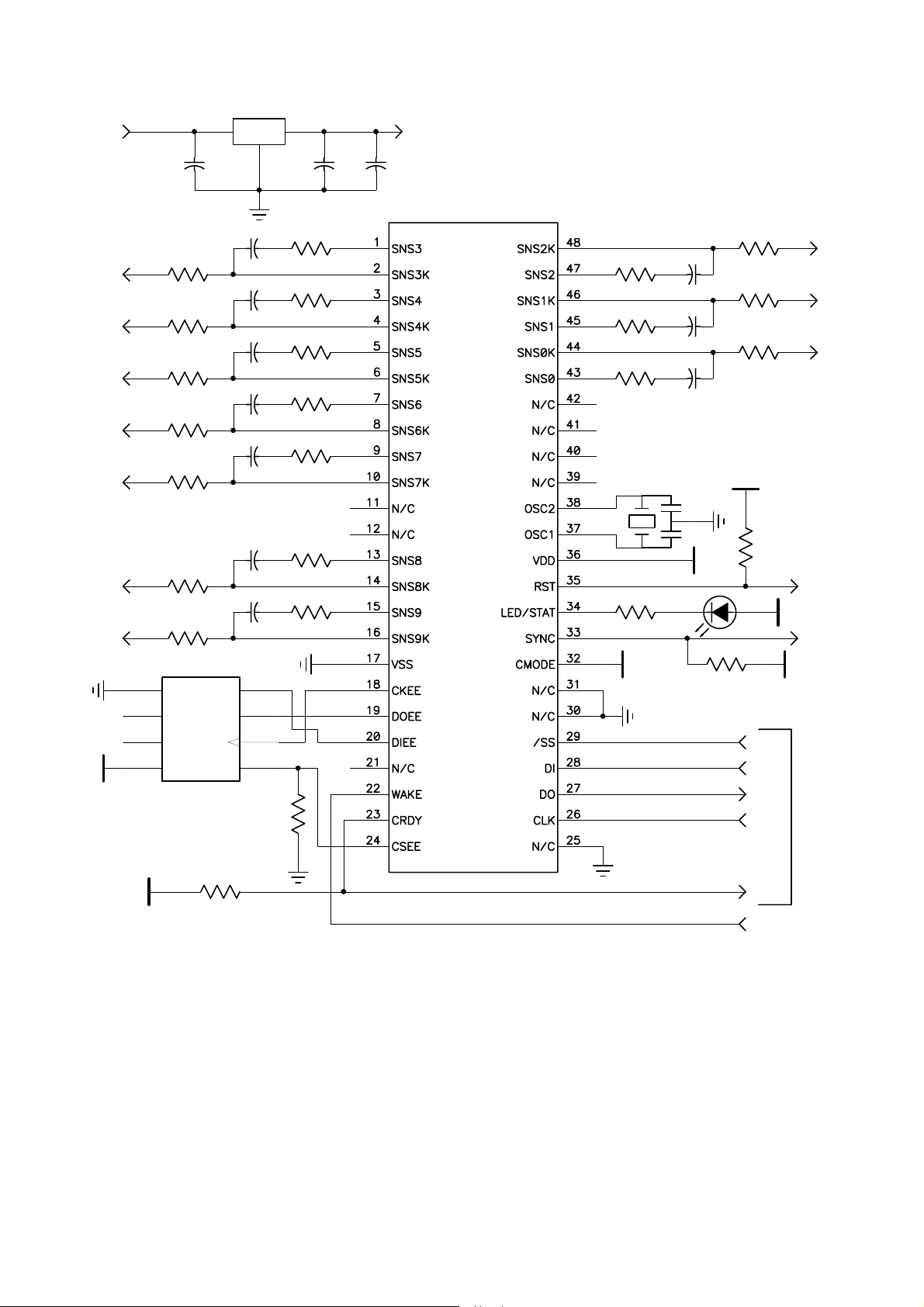
Figure 1.1 SPI Connection Diagram
VUNREG
*10uF
4.7K
KEY3
4.7K
KEY4
4.7K
KEY5
4.7K
KEY6
4.7K
KEY7
Regulator
VI VO
G
22nF
22nF
22nF
22nF
22nF
*4.7uF
2.2K
2.2K
2.2K
2.2K
2.2K
*100nF
VDD
*One bypass capacitor to be tightly coupled to pins 36 and 17.
Follow regulator manufacturer's recommendations
for input and output capacitors.
QT1100A-AS
2.2K
2.2K
2.2K
12MHz 3-TERM
RESONATOR
22nF
22nF
22nF
4.7K
KEY2
4.7K
KEY1
4.7K
KEY0
VDD
2.2K
DIN
CS
22nF
2.2K
22nF
4
3
2
1
10K
VDD
KEY8
KEY9
5
6
7
8
VDD
4.7K
4.7K
VSS
NC
CLK
NC
VDD
93LC46A
DOUT
22K
Note 1: EEPROM is optional when using SPI interface.
Note 2: See Table 1.4 for unused pin connections.
4.7K
VDD
VDD
22K
22K
/SS
DI
DO
CLK
CRDY
WAKE
RESET
VDD
SYNC
VDD
SPI TO/FROM HOST
LQ
9
Copyright © 2003-2005 QRG Ltd
QT1100A-ISG R3.02/1105
Page 10
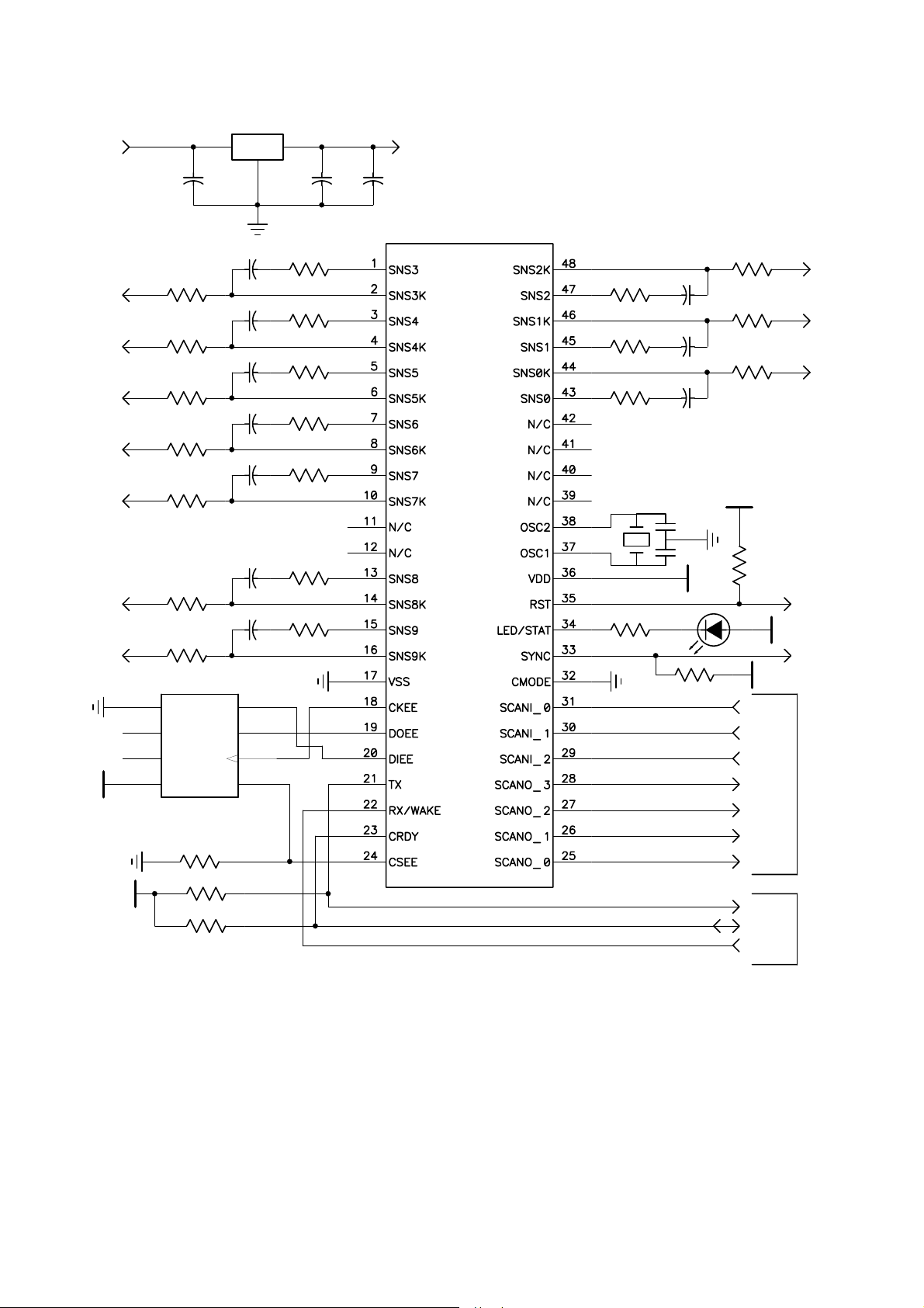
Figure 1.2 UART / Scanport Connection Diagram
Shown with optional EEPROM
VUNREG
*10uF
4.7K
KEY3
4.7K
KEY4
4.7K
KEY5
4.7K
KEY6
4.7K
KEY7
Regulator
VI VO
G
22nF
22nF
22nF
22nF
22nF
2.2K
2.2K
2.2K
2.2K
2.2K
*4.7uF
*100nF
VDD
*One bypass capacitor to be tightly coupled to pins 36 and 17.
Follow regulator manufacturer's recommendations
for input and output capacitors.
QT1100A-AS
2.2K
2.2K
2.2K
12MHz 3-PIN
RESONATOR
22nF
22nF
22nF
4.7K
KEY2
4.7K
KEY1
4.7K
KEY0
VDD
VDD
KEY8
KEY9
VDD
VSS
5
NC
6
NC
7
VDD
8
4.7K
4.7K
DOUT
DIN
CLK
93LC46A
10K
10K
22K
CS
2.2K
22nF
2.2K
22nF
4
3
2
1
4.7K
22K
VDD
22K
VDD
SCANI_0
SCANI_1
SCANI_2
SCANO_3
SCANO_2
SCANO_1
SCANO_0
TX
CRDY
RX/WAKE
RESET
VDD
SYNC
SCANPORT
TO/FROM HOST
UART
TO/FROM HOST
Note 1: EEPROM is optional when using UART interface in this drawing.
Note 2: UART interface is not normally used when using Scanport interface and vice versa.
Note 3: See Table 1.1 for unused pin connections
LQ
10
Copyright © 2003-2005 QRG Ltd
QT1100A-ISG R3.02/1105
Page 11
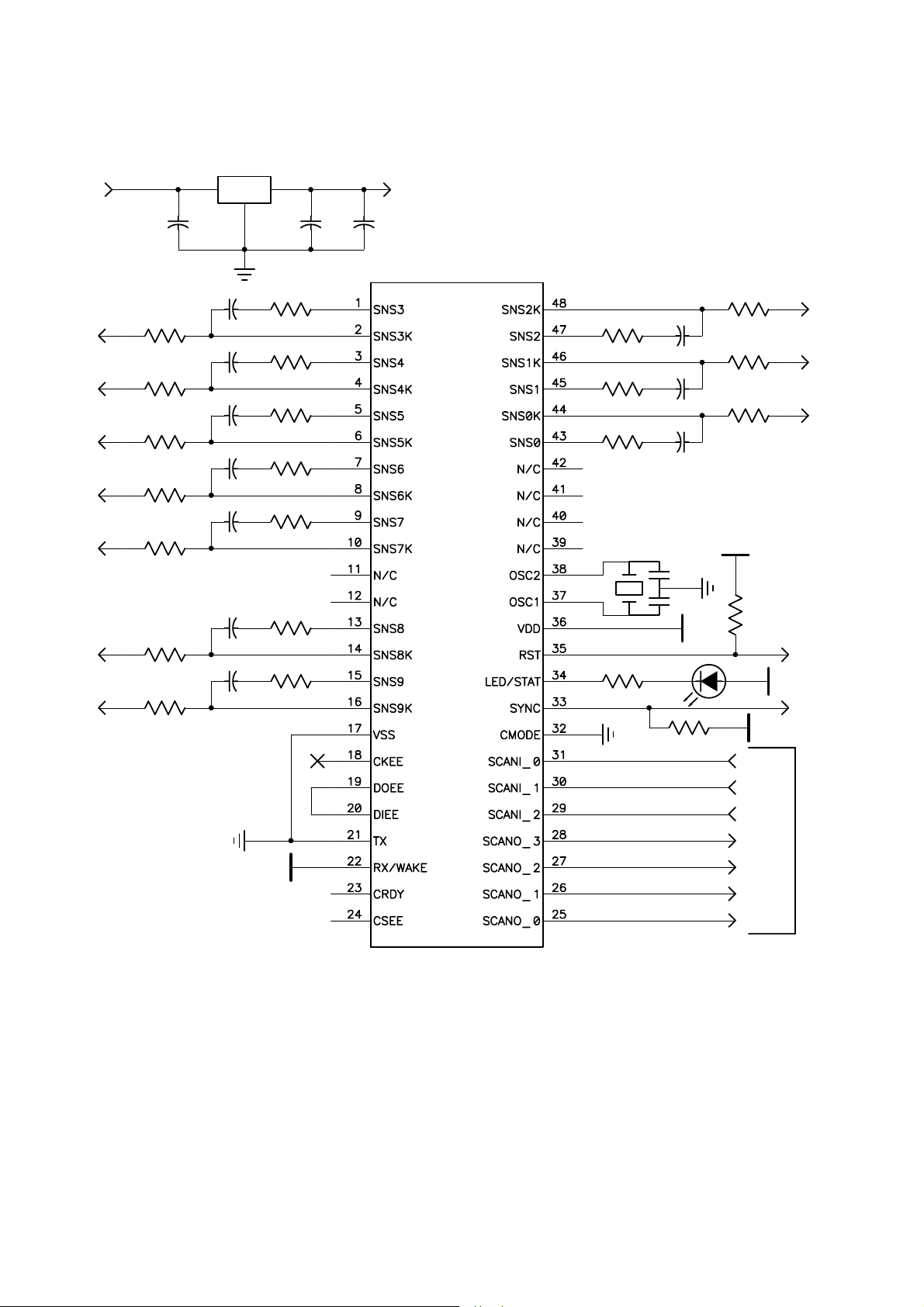
Figure 1.3 Scanport Only Connection Diagram+
Without EEPROM
KEY3
KEY4
KEY5
KEY6
KEY7
KEY8
KEY9
VUNREG
*10uF
4.7K
4.7K
4.7K
4.7K
4.7K
4.7K
4.7K
Regulator
VI VO
G
22nF
22nF
22nF
22nF
22nF
22nF
22nF
2.2K
2.2K
2.2K
2.2K
2.2K
2.2K
2.2K
*4.7uF
*100nF
VDD
*One bypass capacitor to be tightly coupled to pins 36 and 17.
Follow regulator manufacturer's recommendations
for input and output capacitors.
QT1100A-AS
2.2K
2.2K
2.2K
12MHz 3-PIN
RESONATOR
4.7K
22K
22nF
22nF
22nF
VDD
4.7K
KEY2
4.7K
KEY1
4.7K
KEY0
VDD
22K
RESET
VDD
SYNC
VDD
SCANI_0
LQ
SCANI_1
SCANI_2
SCANO_3
VDD
11
Copyright © 2003-2005 QRG Ltd
SCANO_2
SCANO_1
SCANO_0
SCANPORT
TO/FROM HOST
QT1100A-ISG R3.02/1105
Page 12

2 Device Control & Wiring
2.1 Oscillator
The QT1100A uses an external 12MHz resonator as its
frequency reference. This frequency can be lowered for
lower average power, however all functions will also slow
down including response time and communications
parameters. It is not advised to change the operating
frequency without a good reason.
The oscillator source can be from an external circuit, so that
two or more circuits can share the same oscillator. If an
external frequency source is used, it should be fed to OSC1,
pin 37. OSC2 should be left open-circuit.
2.2 Spread Spectrum Modulation
The device features spread spectrum modulation of its
acquisition bursts to dramatically reduce both RF emissions
and susceptibility to external AC fields. This feature cannot
be disabled or modified.
Spread spectrum modulation works together with the
detection integrator (‘DI’) process to eliminate external
interference in almost all cases.
2.3 Cs Sample Capacitors
The Cs sample capacitors accumulate the charge from the
key electrodes and determine sensitivity . (See Section 2.4)
The Cs capacitors can be virtually any plastic film or low to
medium-K ceramic capacitor. The ‘normal’ Cs range is 2.2nF
to 100nF depending on the sensitivity required; larger values
of Cs require higher stability to ensure reliable sensing.
Acceptable capacitor types for most uses include PPS film,
polypropylene film, and NP0 and X7R ceramics. Lower
grades than X7R are not advised.
The Cs capacitors and all associated wiring should be
placed and wired very tight to the body of the IC for noise
immunity to very high frequency RF fields. See Section 2.7.
2.4 Sensitivity
Sensitivity can be altered to suit various applications and
situations on a key-by-key basis. One way to impact
sensitivity is to alter the value of each Cs when the device is
in NTM = 0 mode (see page 25); higher values of Cs will
yield higher sensitivity; each key has its own Cs value and
so can be adjusted independently. The Setups block can
also be used to alter sensitivity, using an external EEPROM,
serial communications, or both (Section 4.1).
Sensitivity can also be increased by using bigger electrode
areas, reducing panel thickness, or using a panel material
with a higher dielectric constant (e.g. glass instead of
plastic).
In some cases the keys may be too sensitive. Gain ca n be
lowered by:
a) making the electrode smaller, or,
b) making the electrode into a sparse mesh using a high
space-to-conductor ratio, or,
c) by decreasing the Cs capacitors (if NTM = 0).
Sensitivity trimming is usually done through a process of trial
and error, using a range of ‘standard fingers’ made of
earthed conductive rubber on the end of a plastic rod.
2.5 Sensitivity Balance
A number of factors can cause sensitivity imbalances among
the keys. Notably, SNS wiring to electrodes can have
differing stray amounts of capacitance to ground, perhaps
due to trace length differences or the presence of ground,
power, or other signal wiring near the SNS traces. Increasing
load capacitance (Cx) will cause a decrease in gain. Key
size differences, and proximity to other metal surfaces can
also impact gain.
The keys may thus require ‘balancing’ to achieve similar
sensitivity levels. The NTHR parameter in the Setups
functions is one easy way to trim and balance key sensitivity
(Section 4.1).
Balancing can also be achieved by adjusting the Cs
capacitor values to achieve equilibrium. The Rs resistors
have no effect on sensitivity and should not be altered. Load
capacitance to ground (to boost Cx) can also be added to
overly sensitive channels to reduce gain; these should be on
the order of a few picofarads.
2.6 Power Supply
The power supply can range from 3.3 to 5.0 volts. If this
fluctuates slowly with temperature, the device will track and
compensate for these changes automatically with only minor
changes in sensitivity. If the supply voltage drifts or shifts
quickly, the drift compensation mechanism will not be able to
keep up, causing sensitivity anomalies or false detections.
The power supply should be locally regulated using a
3-terminal device. If the supply is shared with another
electronic system, care should be taken to ensure that the
supply is free of digital spikes, sags, and surges which can
cause adverse effects.
For proper operation a 0.1µF or greater bypass capacitor
must be used between Vdd and Vss; the bypass cap acitor
should be routed with very short tracks to the device’s Vss
and Vdd pins.
2.7 PCB Layout and Construction
Ground Planes: The PCB should if possible include a
copper pour under and around the IC, but not under the SNS
lines after the Rsns resistors. Ground planes increase
loading capacitance (Cx) on the SNS lines and can
dramatically degrade sensitivity.
Part Placement: The resistors and capacitors associated
with each key should be placed physically as close to the
body of the QT1100A as possible, with the shortest possible
trace lengths, to minimize the influence of external fields
(see Section 2.9.2). The QT1100A should be placed as close
to the key electrodes as possible to reduce wiring lengths, to
minimize stray capacitances on and between SNS traces
and to reduce interference problems.
PCB Cleanliness: All capacitive sensors should be treated
as highly sensitive analog circuits which can be influenced
by stray conductive leakage paths. QT devices have a basic
resolution in the femtofarad range; in this range, there is no
such thing as ‘no-clean flux’. Flux absorbs moisture and
becomes conductive between solder joints, causing signal
drift, false detections, and transient instabilities. Conformal
coatings will trap in existing amounts of moisture which will
then become highly temperature sensitive.
The designer should specify ultrasonic cleaning as part of
the manufacturing process, and in cases where a high level
of humidity is anticipated, the use of conformal coatings after
cleaning to keep out moisture.
LQ
12
Copyright © 2003-2005 QRG Ltd
QT1100A-ISG R3.02/1105
Page 13

2.8 ESD Protection
Normally, only a series resistor is required for ESD
suppression. A 10K to 22K Rsns resistor in series with each
sense trace to each key is normally sufficient. The dielectric
panel (glass or plastic) usually provides a high degree of
isolation to prevent ESD discharge from reaching the circuit.
The Rsns resistors should be placed close to and wired
tightly to the chip, not the keys.
If the Cx load is high, Rsns can prevent total charge and
transfer and as a result gain can deteriorate. If a reduction in
Rsns increases gain noticeably, the lower value should be
used. Conversely, increasing the Rsns can result in added
ESD and EMC benefits provided that the increase in
resistance does not decrease sensitivity.
2.9 Noise Issues
2.9.1 LED Traces and Other Switching Signals
Digital switching signals near the SNS lines will induce
transients into the acquired signals, deteriorating the SNR
performance of the device. Such signals should be routed
away from the SNS lines, or the design should be such that
these lines are not switched during the course of signal
acquisition (bursts).
LED terminals which are multiplexed or switched into a
floating state and which are within or physically very near a
key structure (even if on another nearby PCB) should be
bypassed to either Vss or Vdd with at least a 10nF capacitor
of any type, to suppress capacitive coupling effects which
can induce false signal shifts. LED terminals which are
constantly connected to Vss or Vdd do not need bypassing.
2.9.2 External Fields
External AC fields (EMI) due to RF transmitters or electrical
noise sources can cause false detections or unexplained
shifts in sensitivity.
The influence of external fields on the sensor is reduced by
means of the Rsns series resistors. The Cs capacitors and
the Rsns resistors form a natural low-pass filter for incoming
RF signals; the roll-off frequency of this network is defined
by -
FR=
If for example Cs = 4.7nF, and Rsns = 10K, the EMI rolloff
frequency is ~3.4kHz, which is much lower than most noise
sources (except for mains frequencies i.e. 50/60Hz).
Rsns and Cs must both be placed very close to the body of
the IC so that the lead lengths between them and the IC do
not form an unfiltered antenna at very high frequencies.
PCB layout, grounding, and the structure of the input
circuitry have a great bearing on the success of a design to
withstand electromagnetic fields and be relatively noise-free.
These design rules should be adhered to for best ESD and
EMC results:
1. Use only SMT components.
2. Keep all Cs, Rs, Rsns, and the Vdd/Vss bypass
capacitor components wired tightly to the IC.
3. Place the QT1100A as close to the keys themselves as
possible.
4. Do not place electrodes or associated wiring near
other signals, or near a ground plane. If a ground plane
is unavoidable, keep the SNS tracks very thin (e.g.
2✜R
1
SNSCS
0.15mm) and relieve the ground plane widely around
them (e.g. 5mm clear space on all sides).
5. Do use a ground plane under and around the chip
itself, back to the regulator and power connector (but
not beyond the Rs/Cs/Rsns networks).
6. To prevent cross interference, do not place an
electrode or SNS traces of one QT1100A near the
electrode or the SNS traces of another QT1100A or
similar device, unless they are synchronized with a
Sync signal in a way that adjacent traces and keys do
not have acquisition bursts on them at the same time.
7. Keep the electrodes (and wiring) away from other
traces carrying AC or switched signals.
8. If there are switched LEDs or related wiring near an
electrode or SNS traces (e.g. for backlighting of a key),
bypass the switched traces to ground.
9. Use a voltage regulator just for the QT1100A to
eliminate noise coupling from other switching sources
via Vdd. Make sure the regulator’s transient load
stability provides for a stable, settled voltage just
before each burst commences.
2.10 Start-up Time
After a reset or power-up event, the device requires 400ms
to read the EEPROM, if one is connected, initialize the
device, and start acquiring signals. After this time, the part
will calibrate all keys. The calibration time depends on the
burst spacing but is about 450ms for a burst spacing of 3ms.
This time is proportional to the burst spacing (Section 4.14).
The burst spacing governs the time from the start of one key
acquisition cycle to the next, and can be set via serial Setups
or via the external EEPROM. Thus, the total start-up time
after a reset is about 850ms if the burst spacing is set to
3ms.
The device will communicate immediately after the Setup
block is loaded (from EEPROM. if any, or from defaults).
2.11 Operating Parameter Setups
The device features a Setups block area in internal RAM that
holds numerous configuration parameters determin ing how
the part will operate. Each key can be configured individually
for a wide variety of parameters as discussed in Section 4. In
addition, the device can be configured for the AKS ™ function
which treats participating keys as a group in which only the
key with the strongest signal will generate a response.
Standalone (with EEPROM) Setups: In standalone mode
with EEPROM, device setups are configured using an
external 93LC46A byte-mode EEPROM (see Table 1.2, page
5). This part can be programmed separately using a
commercially obtainable programm ing device then inserted
into the circuit, or, it can be programmed using a QT1100A in
serial mode via a PC interface with the 93LC46A in a socket
so that it can be transferred to the target PCB.
The EEPROM contents and default values are detailed in
Table 4-1, page 31. The last EEPROM entry should be a
CRC check byte. If the CRC byte is set to 0xD6, the CRC will
be ignored.
In standalone mode the EEPROM must have the first byte in
location 0 set to the value 0xD6 for the EEPROM to be read.
The rest of the Setup table must follow, starting at location 1
in the EEPROM.
LQ
13
Copyright © 2003-2005 QRG Ltd
QT1100A-ISG R3.02/1105
Page 14

Without the EEPROM the QT1100A will operate in a default
mode, designed to accommodat e most touch sensing
requirements (Section 2.12, below).
Serial Mode Setups: The two serial interfaces permit a
host MCU to program control setups into the QT1100A on
power-up or even during normal operation, allowing low cost
reconfigurability. This is performed with a block of data,
referred to as a Setups block.
The Setups block must end with a CRC check byte. If the
optional 93LC46A EEPROM is also used, the Setups block
will be stored locally so that there is no need to reload after
each power-up.
2.12 Standalone Operation, No EEPROM
The device can operate in Standalone Mode without serial
communications or EEPROM using only its parallel scanport
interface. (See Table 1.3, page 6 and Figure 1.3, page11)
There are some minor differences in the default settings and
behaviour in Standalone Mode without EEPROM compared
with other modes:
1. K2L is enabled on all keys*
2. SYNC is enabled (SE = 1)*
3. No serial comms - CRDY is always clamped low
*These exceptions are noted in Table 4-1, page 31.
2.13 EEPROM Functionality
The serial EEPROM is used to store Setups information
which alters the device behavior. If the EEPROM is not used,
the device uses default parameters to operate , or,
customized parameters loaded into the device via serial
interface.
The EEPROM’s functionality is not necessary when used
with a serial interface. The host serial controller can send the
Setups to the QT1100A following each power-up. In a serial
mode, the EEPROM eliminates the need to send Setups
after each power-up since they are stored locally.
The EEPROM must contain the value 0xD6 as its first byte
or it will not be read. The table on page 31 shows the
contents required for this EEPROM. A CRC must be
appended to the end of the EEPROM table, or, the CRC can
be replaced by a 0xD6 code, in which case no CRC
checking will be performed (not recommended except as a
development shortcut). A blank EEPROM will be
programmed properly when the host sends a Setups block to
the device.
EEPROM corruption is automatically detected every 2
seconds during normal run operation . If the EEPROM is
found to be corrupt or erased, the EEPROM error flag is set
in the device status byte (command 0xC2); the EEPROM
itself is not corrected. If the device is using serial
communications, the host controller should reload the
Setups and then reset the device.
If in a serial mode an EEPROM is not installed, pin DIEE
should be connected to Vdd.
2.14 Scanport Interface
The scanport functions as a ‘legacy replacement’ for a matrix
scanned XY keyboard. Single inputs (one-of-three) on
Scan_In lines result in a pattern of bits on Scan_out pins
depending on the keys that are active. If no keys are active
the Scan_out pins remain inactive. See connection pinlists,
Tables 1.1 and 1.2.
All logic on the scanport is ‘active high’ for both Scan_In and
Scan_Out. The scanport maps to the Scan_ In and Scan_Out
pins as per Table 2.1.
Table 2.1 - Scanport I/O Mapping
Scan Out
0
Scan In 0
Scan In 1
Scan In 2
The scanport is enabled if the CMODE pin is strapped low .
The UART is also enabled in this mode but it can be ignored ;
if UART serial is not used, TX should be connected to Vss.
Scanport Latency: The latency of the scanport from
Scan_In to Scan_Out is 120µs maximum. UART transfers do
not affect this response time. Scanning software has to take
this delay into account, i.e. it should not expect the
Scan_Out pins to be stable until 120µ s after setting the
Scan_In pins.
One easy way to use the scanport is to read the scanport
before changing the Scan_In signals. Normally, Scan_In
should be changed to a new state every 1 ~ 2ms. Faster
scanning than this will not result in a perceptibly faster
response time. Therefore, if the Scan_Out lines are read
immediately before changing the Scan_In signals, the host
controller will not have to wait for the 120µs scanport
latency.
System Response Time: The setting of the two detection
integrators (see Section 4.9) strongly affects the basic
device response time. The host’s scan rate adds to this time.
If the basic QT1100A response time is set to 80ms, and the
host completely scans the device every 50ms, the total
response time can be a very slow 130ms.
One way to maintain good response time while minimizing
host activity is to have the host monitor the LED/STAT pin,
perhaps via interrupt, and service the scanport only when the
LED/STAT pin becomes active. (See Section 4.8, page 27)
Sleep/Wake Function: Sleep/Wake can only be used in
conjunction with a serial mode which sets the sleep state via
a command, and so Sleep is not possible in Scanport mode
without a serial interface.
Sync Mode with Scanport: Sync mode can be enabled
using an EEPROM having the correct Setups; Sync mode
also works in standalone mode without an EEPROM (see
also Section 4.12). In Sync mode the acquire bursts are
synchronized to the external clock source; the scanport will
operate correctly while the device is waiting for a sync edge.
Scan Out
Scan Out
1
2
Scan Out
3
Key 3Key 2Key 1Key 0
Key 7Key 6Key 5Key 4
00Key 9Key 8
2.15 Start-up Sequencing
After power-up or reset the flag ‘Reset Occurred ’ will be set.
The user can read this flag with command 0xC2. This flag
can be reset by issuing a ‘0xC2 0xC7’ command sequence.
If an EEPROM is installed and the EEPROM’s CRC does not
match its contents, or the first byte is not 0xD6, the error flag
“EEPROM Error” will be set. In this case, the default Setup
settings will be used but the EEPROM contents will stay
unchanged.
2.16 Error Detection and Reporting
A ‘major error’ is one where an enabled key signal falls
below LBLL (Section 4.13) or rises above a value of 4095 , or
where there is a CRC error in RAM or EEPROM Setups. The
LQ
14
Copyright © 2003-2005 QRG Ltd
QT1100A-ISG R3.02/1105
Page 15

former can occur if the Cs capacitor fails or there is a short
in the SNS circuit; if this happens , the affected key is shut
down immediately and the key is switched off.
Keys that are intentionally disabled will not burst, and so
cannot show an error. In standalone mode with no EEPROM
present (Scanport mode), keys are disabled by strapping the
SNS pins to ‘unused’ settings (Table 1.1 page 4), and this
will not generate a ‘major error’, unless the error occurs after
the part has gone through power-up calibration successfully
without detecting that the key is disabled via SNS pin
configuration.
In any mode that uses an EEPROM or uses either UART or
SPI communications, keys must be disabled by setting the
NTHR parameter to zero for the key(s) (Section 4.1). If in
EEPROM or serial mode a key is disabled via SNS pin wiring
only, it will be classified as a ‘major error’.
control. The UART mode operates in the same way and with
the same protocol and commands as the SPI interface.
UART mode is selected by strapping the CMODE pin low.
UART mode and Scanport mode can operate together. If
only UART mode is desired, the Scan_In pins need to be
grounded. If only the Scanport is used, the UART can be
ignored. An unused RX line should be connected directly to
Vdd.
UART transmission parameters are (Fosc = 12MHz):
Baud rate options: 4800, 9600, 19.2K, 28.8K
Start bits: 1
Data bits: 8
Parity: None
Stop bits: 1
UART Operation with Scanport: Scanport and UART
operation can be used together. (See Section 2.14)
3 Serial Operation
There are two serial interfaces in the QT1100A: UART, and
SPI.
UART provides a simple solution using well known
asynchronous signalling. Many MCUs contain UART or
USART blocks which are perfectly suited to this mode.
MCUs without a UART hardware function can easily use a
firmware UART function in most cases. The chief advantage
of UART mode is wiring simplicity: only 3 wires, (TX, RX, and
CRDY) are required.
SPI communications are based on the well known
synchronous interface used extensively between
microcontrollers and peripherals. The QT1100A uses
slave-only SPI mode. This interface does not require an
accurate clock rate, and can operate faster than UART
mode. However, SPI operation requires 5 wires.
The host device always initiates communications
sequences; the QT1100A is incapable of chattering data
back to the host. A command from the host to the QT1100A
always ends in a one or more byte response from the
QT1100A. Some transmission types from the host require
the use of a CRC check byte to provide for robust
communications. This command/response design is
intentional for FMEA purposes so that the host always has
total control over the communications with the QT1100A.
Effectively this behavior forces designs to have inherently
self-checking ‘loop back’ characteristics.
System Response Time: The setting of the two detection
integrators (see Section 4.9) strongly affects the basic
device response time. The serial poll rate adds to this
response time. If the basic QT1100A response time is 80ms,
and the host polls the device every 50ms, the total response
time can be a very slow 130ms. Normally, the host should
poll the QT1100A every ~10ms to minimize delay ‘stacking’.
To minimize delays further, the command 0xC9 can be used
(‘Quick 1st Key’; see Section 3.5.14) instead of 0xC0.
One way to improve speed while minimizing host activity is
to have the host monitor the LED/STAT pin, perhaps via
interrupt, and service the device with a 0xC0 or 0xC9
command only when the LED/STAT pin becomes active.
(See Section 4.8)
3.1 UART Interface
UART mode allows a host device to communicate
conveniently over two serial wires asynchronously, with a
handshaking line (CRDY) to provide bidirectional data flow
3.1.1 TX Pin
The TX pin has an open-drain drive to allow bussing with
other similar parts. The TX line can thus be shared with other
UART based peripherals such as a second QT1100A.
TX must be pulled high to Vdd with a resistor in UART mode.
The resistor value will depend on the total amount of stray
capacitance on TX - more capacitance will require lower
values of pull-up resistor, especially at higher Baud rates.
The risetime of the signals on this line should be 1/10th of
the bit width, i.e., if running at 9600 Baud, the bit width is
about 100µs, and the risetime should be 10µs or less. In
most cases, a 47K resistor is low enough, however this
should be confirmed using an oscilloscope.
An unused TX pin should be connected to Vss.
3.1.2 Sleep/Wake Operation in UART Mode
The device can be put into sleep mode with a serial
command (0x05). The device can sleep for up to 700ms;
some time after this it will self-reset. The Wake and RX
functions are on the same pin, which allows a host to
conveniently wake the device with a dummy character (e.g.
0x00 null) before communicating with it. Wake operates on
the falling edge; the negative-going level must be at least
40µs wide to be recognized.
See also Section 3.4.6.
3.1.3 CRDY Operation in UART Mode
The CRDY serial handshake pin is open-drain and requires a
10K ~ 220K pull-up to Vdd. Either the host or the QT1100A
can pull down on this line to stop data flow (wire d-AND
logic). If CRDY is high the communications can flow in either
direction. The host should obey this control line or overruns
and transmission errors will occur in the device.
Host-to-QT1100A UART CRDY Behavior: If the CRDY line
is released by the host but the CRDY line stays low, this
means the QT1100A is busy and cannot accept
communications. The host must wait for the CRDY line to
float high again before it can send the byte. If the CRDY line
happens to go low again just as the host is about to send a
byte, the host has a 10µs grace period in which it can still
initiate the transmission. This is acceptable for most MCU
types, however even fast PCs operating under Windows
have a difficult time responding within the 10µs grace period
and this can result in frequent transmission errors.
QT1100A-to-Host UART CRDY Behavior: When the
QT1100A needs to send data back to the host, it will release
the CRDY line (if not already released) and wait for it to float
LQ
15
Copyright © 2003-2005 QRG Ltd
QT1100A-ISG R3.02/1105
Page 16

high before sending a byte. If the host is busy and cannot
accept data, it should clamp CRDY low until it is ready.
Before each return byte is sent, the QT1100A will check
CRDY in this manner and wait until the host is ready before
sending.
The host should allow a 10µs grace period in which it can
still accept data from the QT1100A after it releases CRDY
high, to allow for any delays in the response from the sensor.
CRDY / Burst Behavior: The pacing of CRDY and the
transmission of UART data are interleaved with acquisition
bursts. The QT1100A cannot send or receive data during a
burst or for a short time thereafter. CRDY is forced low by
the QT1100A when a burst is taking place and
communication is not possible. At the fastest burst spacing,
there is at least a 250µs window of time between bursts
when communications can take place and CRDY is high.
If a serial transmission from QT1100A to host is occurring
when a burst should be starting, the communications takes
precedence and the next acquisition burst is delayed.
3.2 SPI Operation
Refer to page 38 for timing diagram.
The SPI mode allows a host device to communicate
conveniently using four control lines synchronously, with a
CRDY handshaking line to provide control flow. The SPI
mode operates in the same way and with the same protocol
and commands as the UART interface. However whereas
the UART mode permits the QT1100A to send back
responses to the host under its own volition, the SPI mode is
a slave mode only requiring the host to always generate the
shift clock.
Where a response is expected back from the QT1100A, the
host can shift over a dummy null (0x00) command to the
QT1100A which will be ignored. The host should not overlap
commands with responses. Thus, if there are two expected
response bytes to a command, the host can send and shift
back the following bytes:
QT1100A ResponseHostShift #
1
2
3
SPI transmission parameters are (Fosc = 12MHz):
Transmission mode: Slave-only
Clock rate: 100kHz max
Clock duty cycle: 50%
Data bits: 8
Clock idle: High
Clock shift out edge: Falling
Clock shift in edge: Rising
Delay from shift in edge: None
*Note that the QT1100A returns a 0x55 dummy byte with a
host command.
If a command is not recognized, the response on the next
shift will be 0x55.
3.2.1 Multi-Drop SPI Capability
In SPI mode the DO pin floats while /SS is high to allow the
SPI lines to be shared with other devices. A 10K ~ 20K Ohm
pull-up resistor should be used on this pin to prevent DO
from freely floating.
0x55 (see below*)Command_A
Response_1 to ANull
Response_2 to ANull
0x55 (see below*)Command_B4
When used with other similar devices, each QT1100A part
should have its own /SS and CRDY connections back to the
host controller; the other SPI lines can all be shared.
3.2.2 Sleep/Wake Operation in SPI Mode
The device can be put into sleep mode with a serial
command (0x05). The device can sleep for up to 700ms;
some time after this it will self-reset. Wake operates on the
falling edge; the negative-going level must be at least 40µs
wide to be recognized.
The Wake pin can be connected to /SS, and the host can
then wake the device from sleep using a >40µs negative
dummy pulse on /SS.
See also Section 3.4.6.
3.2.3 CRDY Operation in SPI Mode
CRDY is an open-drain line requiring a 10K ~ 220K Ohm
pull-up resistor. The QT1100A will pull down on this line to
stop data flow from the host. The QT1100A does not
respond to the host pulling CRDY low in SPI mode, since the
host is always in control of all data transmissions. CRDY is
unidirectional (QT1100A to Host) in SPI mode.
The host must wait for CRDY to float high before it can clock
the SPI interface. If CRDY happens to go low again just as
the host is about to clock data, the host has a 10µs grace
period in which it can still initiate /SS (slave select) even
though CRDY has already gone low.
CRDY / Burst Behavior: The pacing of CRDY and the
transmission of UART data are interleaved with acquisition
bursts. The QT1100A cannot send or receive data during a
burst or for a short time thereafter.
CRDY is forced low by the QT1100A when a burst is taking
place and communication is not possible. At the fastest burst
spacing, there is at least a 250µs window of time between
bursts when communications can take place and CRDY is
high. Similarly, if the burst duration exceeds its timeslot, the
device will ensure that there is an additional 250µs
appended to the burst to allow for communications.
If a serial transmission is occurring when a burst should be
starting, the communication takes precedence and the next
acquisition burst is delayed. Therefore, the 250µs should be
viewed as a minimum which can expand to meet the needs
of a single byte transmission. Additional bytes will usually
occur in the next timeslot.
3.3 Communication Error Handling
If a communications error takes place, the host should
recover by issuing a ‘Return Last Command’ command
(0xC7) at least twice to make sure the QT1100A and host
are communicating properly with each other.
3.4 Control Commands
Control commands are used to place the device into special
modes or cause the device to reset, calibrate or run. (See
summary Table 3-1, page 23)
3.4.1 Null Command - 0x00 (SPI Only)
This command is used primarily to shift back data from the
QT1100A in SPI mode. Where a response is expected back
from the QT1100A after a command, the host should shift
over a null for each expected byte.
LQ
16
Copyright © 2003-2005 QRG Ltd
QT1100A-ISG R3.02/1105
Page 17

Since the host device is always the master in SPI mode, and
data are clocked in both directions, the null command is
required to act as a placeholder where the requirement is to
get data back from the QT1100A. See also Section 3.2.
In UART mode there is no response whatsoever to a null
command.
3.4.2 Enter Setups Load Mode - 0x01
This command is used to load the Setups block into the
device over either serial interface. See Table 4-1 on page 31
for reference.
The command must be repeated 2 times within 100ms or the
command will be aborted (not reset); the repeat of the
command must be sequential without any other intervening
command or even a null.
250µs worst case after receipt of the second 0x01, the
device will start to send back the response byte 0x53
(signalled using CRDY as always, i.e. the response could be
delayed beyond 250µs by the host itself, either via a late
shift operation in SPI Mode or via holding CRDY low in
UART mode).
If no 0x53 is returned, the command was not properly
received; the host should recover by issuing a ‘Return Last
Command’ command (0xC7) at least twice to make sure the
QT1100A and host are communicating properly with each
other, and then the 0x01 commands should be sent again.
From this point on the host should send the Setups block
including the ending CRC byte as a stream to the QT1100A,
without interruption, paced only by the CRDY line. During
this time the chip suspends its normal acquisition bursts.
The time between bytes can be from 10µs to a limit of
100ms.
If a data timeout occurred in the block load (the time
between any two sequential block data bytes exceeded
100ms) a response of 0xF1 will immediately be attempted
back to the host, the Setup block sequence will be aborted,
and the chip will reload the Setup block from the EEPROM
(if available and correct) or from ‘factory defaults’. A device
reset will automatically occur if the QT1100A does not
receive a further command (any of 0x01, 0x02, 0x03 or
0x04) within 1s after the block sequence has suspended due
to a timeout error.
The host should listen for a 0xF1 response while shifting the
Setups block to terminate and restart the Setups load
sequence if required.
Note that in SPI mode, all responses must be shifted out
with nulls shifted over by the host.
EEPROM not present: If no EEPROM is installed and DIEE
is tied to Vdd, the QT1100A will check the CRC and reply
with a response byte:
0xF0 - CRC not OK, and as a result block load failed
0xF1 - transfer timeout; time between bytes >100ms
0xFE - block loaded OK, CRC is OK
In the case of either 0xF0 or 0xF1, the QT1100A will load
‘factory defaults’ into the device (when no EEPROM is
present).
With no EEPROM present, the delay between the CRC byte
sent to the QT1100A and the response back from the
QT1100A is 800µs maximum (signalled using CRDY).
EEPROM present: With an EEPROM installed, the device
will check the CRC and if valid, start programming the
EEPROM with the new Setup block, and check that the
EEPROM is written correctly. It will respond as follows:
0xF0 - CRC is not OK, and as a result block load failed
0xF1 - transfer timeout; time between bytes >100ms
0xF2 - block loaded OK, but EEPROM write failed
0xFE - block loaded OK, CRC is OK, EEPROM write OK
(0xFE response requires up to 370ms due to
EEPROM write time - this is dependent largely on the
EEPROM’s write time specification)
If there is no response from the device within 370ms after
the block has been completely sent , the command was not
properly received and the device should preferably be reset
using the RST pin before attempting the command again.
Only if the entire Setup block is received without error and
the CRC is OK (or 0xD6 for testing; see below) will the
Setups information be recorded to EEPROM.
At the end of the full command sequence the device remains
suspended (acquire bursts are stopped) until a Setups, Run,
Cal, or Reset command is received (0x01, 0x02, 0x03, or
0x04). If one of these commands is not received within 1s
after the block is loaded and the response byte is generated ,
the part resets itself, enters Cal mode, and then runs
automatically.
If there was an error in the Setups load operation, the device
will run either with ‘factory defaults’ (if there was a 0xF2
error) or with previously stored EEPROM data (if there was a
0XF0 or 0xF1 error).
CRC Note: The 0x01 command requires that the ending
CRC byte is calculated by the host on the data block itself
without the 0x01 command itself being folded in to the CRC.
This is a notable exception to the use of CRCs in this device.
Other commands ending in a CRC fold in the command byte
itself as the first byte in the CRC calculation.
Dummy CRC for Testing: For testing purposes, a dummy
CRC byte, of value 0xD6, can be placed at the end of the
Setups block which is always accepted by the QT1100A
even though it is ‘wrong’. While a 0xD6 value will inhibit CRC
checking, the QT1100A will actually compute and record the
correct CRC value into the EEPROM (if present).
Should an actual CRC calculation result in a 0xD6
(probability = 0.39%) and CRC checking is required, the
designer should change one of the unused bits shown in the
Setup table (page 31) to cause the CRC to be something
else.
After a Setups Load: After a successful Setups block load,
there are four basic options:
1. Run the device via the 0x02 command, i.e. without the
benefit of a recalibration, or,
2. Calibrate the device via the 0x03 command, in which
case the device will calibrate all keys and run again, or,
3. Reset the device using the 0x04 command, or,
4. Wait 1 second for the device to enter self-reset.
Changes to NDCR, NRD, AKS, EK, K2L, PDCR, PRD,
PTHR, PHYS, LEDP, LBLL, KEYO, BR or BS do not require
a recalibration to take effect, and it is faster to just issue a
0x02 RUN command after the 0x01 is complete.
Changes to NTHR, NHYS, NDIL, FDIL, and NTM should be
followed with a 0x03 Cal command.
Changes to SE or SYNC should be followed with a device
reset command, RST pin reset, or 1s timeout reset to allow
the new parameters to properly take effect.
LQ
17
Copyright © 2003-2005 QRG Ltd
QT1100A-ISG R3.02/1105
Page 18

3.4.3 Enter Run Mode - 0x02
This command is used only after a Setups Load command
(0x01) has completed to get the device to run as a sensor,
without any key calibration. This is useful to make running
changes, for example in drift compensation rates or
threshold levels, without disturbing key calibrations.
The command must be repeated 2 times within 100ms or the
command will fail; the repeated command must be
sequential without any intervening command , not even a
null. After the second 0x02, the QT1100A will reply with the
character 0xFD when the part begins to run as a sensor. The
delay in responding to the second 0x02 with 0xFD is 250µs
maximum (signalled using CRDY).
If no 0xFD is returned, the command was not properly
received; the host should recover by issuing a ‘Return Last
Command’ command (0xC7) at least twice to make sure the
QT1100A and host are communicating properly with each
other, and then the 0x02 commands should be sent again.
3.4.4 Enter Cal Mode - 0x03
This command is normally used only after a Setups Load
command (0x01) has completed to get the entire device to
calibrate and run as a sensor. Note that on normal power-up
or reset, the device will automatically enter Cal mode
regardless, and then run normally. Therefore the only time
this command is required is when the part is suspended
after a Setups load, or, if there is a need to recalibrate all
keys at one time during normal running.
The 0x1k command is more efficient for recalibrating
individual stuck keys if desired (Section 3.4.7).
The 0x03 command must be repeated 2 times within 100ms
or the command will fail; the repeating command must be
sequential without any intervening command , not even a
null. After the second 0x03 from the host, the QT1100A will
reply with the character 0xFC within 450µs if the command
has been accepted. After the 0xFC response, the device will
initiate calibration of all keys in parallel.
The host can check the progress of calibration by issuing a
0x8k command on the highest enabled key (e.g. key #9); all
the keys being calibrated by 0x03 will have finished
calibrating when the highest key number is done.
The time required to calibrate all 10 keys is 15 complete
acquire cycles, or 15 x 10 keys = 150 timeslots. If the burst
spacing is 4ms, then Cal will require 600ms to calibrate all
10 keys. Disabled keys do not reduce this time.
Afterwards, the host can check error flags to find which
key(s) failed during calibration, if any, for example using
command 0xC2 (Section 3.5.7) or 0xC5 (Section 3.5.10).
This might happen if there is a component failure , short or
open circuit on the PCB.
If no 0xFC is returned, the command was not properly
received; the host should recover by issuing a ‘Return Last
Command’ command (0xC7) at least twice to make sure the
QT1100A and host are communicating properly with each
other, and then the 0x03 commands should be sent again.
3.4.5 Force Reset - 0x04
This command is used to cause the part to reset, in the
same way as a hardware /RST signal.
This command must be repeated 2 times within 100ms or
the command will fail; the repeating command must be
sequential without any intervening command , not even a
null. After the second 0x04 from the host, the QT1100A will
reply with the character 0xFB within 250µs to indicate that it
has been properly received.
If no 0xFB is returned, the command was not properly
received; the host should recover by issuing a ‘Return Last
Command’ command (0xC7) at least twice to make sure the
QT1100A and host are communicating properly with each
other, and then the 0x04 commands should be sent again.
After the part resumes operation, it will set the “Reset
Occurred” flag (see Section 2.15) to indicate there was a
power-up event, and it will go through a complete C al mode
automatically and then run and sense keys normally.
The device will calibrate and run after a delay of 100ms +
150 burst spacings, which could be up to 1. 05s on 7ms burst
spacings. While calibrating, the QT1100A can communicate
serially and the user can track the progress of ongoing
calibrations using command 0x8k.
3.4.6 Sleep - 0x05
This command is useful to allow low average operating
power when in standby mode or when fast response time is
not required. During sleep, the device consumes only a few
microamps of current. Using Sleep mode, it is possible to get
average current consumption down to 100µA while having
the part run with reduced response time. Actual average
current drain will be a function of the ratio of running time to
sleep time.
The 0x05 command must be repeated 2 times within 100ms
or the command will fail. After the second 0x05 from the
host, the device will reply with the character 0xFA within
250µs. The device will then enter a Sleep mode until
awakened by a negative edge or negative pulse on the
WAKE pin (pin 22), at least 40µs, wide or via a hardware
reset on the RST pin. Note that if the device is reset, it will
recalibrate on power-up, which is usually not desirable . If the
device wakes via the WAKE pin , it will resume operation in
the same state from which it went to sleep.
If no 0xFA is returned, the command was not properly
received; the host should recover by issuing a ‘Return Last
Command’ command (0xC7) at least twice to make sure the
QT1100A and host are communicating properly with each
other, and then the 0x04 commands should be sent again.
If the device is not awakened intentionally within 700ms of
entering sleep, the device can go into self-reset causing the
internal states and data to be lost , and a recalibration to be
performed.
In UART mode, the QT1100A can be awakened with a NULL
(0x00) byte. In SPI mode, the QT1100A can be awakened by
connecting pin /SS to WAKE and sending an empty /SS
pulse from the host to the QT.
Wake time: The device requires ~160uS from the WAKE
input to resumption of normal sensing and communications.
3.4.7 Cal Key ‘k’ - 0x1k
Calibrates only key k, where k = {0..9}. Example: The
command 0x14 causes key 4 to calibrate. This command
functions the same as the 0x03 Cal command (Section 3.4.4,
above) except this command only affects one key .
This command must be repeated 2 times within 100ms or
the command will fail; the repeating command must be
sequential without any intervening command , not even a
null.
0x1k returns 0xF8 if the command has been accepted and
will be processed. This response can come up to one burst
LQ
18
Copyright © 2003-2005 QRG Ltd
QT1100A-ISG R3.02/1105
Page 19

timeslot after the second 0xF8 has been received. The user
can then track the progress of the key calibration with the
0x8k command (Section 3.5.4).
If no 0xF8 is returned, the command was not properly
received; the host should recover by issuing a ‘Return Last
Command’ command (0xC7) at least twice to make sure the
QT1100A and host are communicating properly with each
other, and then the 0x1k command should be sent again.
The chosen key ‘k’ is recalibrated in its normal burst
timeslot; normal running of the part is not interrupted and all
other keys operate correctly throughout. This command is for
use only during normal operation to try to recover a single
key that is stuck or has not calibrated correctly.
It is possible to issue several 0x1k commands to several
keys sequentially, however the 0xF8 return value should be
received back from a prior 0x1k command before a new
0x1k command is issued.
3.5 Status Commands
Status commands are used to evoke a response from the
QT1100A, for example to return signal values or to get key
status. See summary Table 3-2 on page 24.
3.5.1 Signal for 1 Key - 0x2k
Returns the raw signal for key k, where k = {0..9}. Example:
The command 0x25 addresses key 5. The value is a 16-bit
number and no CRC is appended to the return, so the return
data should not be considered secure under FMEA rules.
The valid return number range is from 0..4095. The high byte
is returned first.
3.5.2 Reference for Key ‘k’ - 0x4k
Returns the reference level for key k, where k = {0..9}.
Example: The command 0x48 addresses key 8. The value is
a 16-bit number and no CRC is appended to the return, so
the return data should not be considered secure under
FMEA rules. The valid return number range is from 0..4095.
The high byte is returned first.
3.5.3 Detect Integrator for Key ‘k’ - 0x6k
Returns the detect ‘normal’ detect integrator (‘DI’) for key k,
where k = {0..9}. Example: The command 0x63 addresses
key 3. The value is contained in the lower 4 bits of an 8-bit
character, i.e. in the range from 0..15 ; no CRC is appended
to the response, so the return data should not be considered
secure under FMEA rules.
3.5.4 Status for Key ‘k’ - 0x8k
Returns the status bits for key k, where k = {0..9}. Example:
The command 0x87 addresses key 7. The return value is
contained in a single 8-bit character. A CRC is appended to
the return; this CRC includes the command 0x8k itself as the
first byte in the CRC calculation.
The return bits are as follows:
DescriptionBit #
7
6
5
4
3
2
1 = This key is in detect
(volatile)
unused
unused
1 = This key is in process of
detection (but not yet reported
as having detected) (volatile)
1 = This key is undergoing
calibration (volatile)
1 = This key has a cal error
(non-volatile)
1
0
1 = This key is experiencing
extreme signal conditions
(non-volatile)
1 = This key is disabled due
to a Setup configuration or
due to an extreme condition
(non-volatile)
Bit_7: 1 = Active key. The key is indicating a confirmed
touch. This bit is set or cleared dynamically depending on
the state of the DI counter for each key. This bit is will
self-clear when touch is no longer detected.
Bit_4: 1 = Detection pending. The key is in the process of
trying to confirm a detection (the signal is below NTHR),
but has not yet reported as active. Normally this flag is
only used for test purposes. This bit will self-clear when
the key falls out of this state.
Bit_3: 1 = Calibration in progress. The key is in the
process of calibration. This bit will self-clear when the
calibration is complete.
Bit_2: 1 = Cal error. There was an error on this key the last
time it attempted a calibration. This means an overflow
(signal >4095) or underflow (see Section 4.13, page 29)
occurred during a cal cycle for that key. This bit is
determined only after a Cal of the key in question (either
via Cal 0x03 or 0x1k commands). After Reset, these bits
are cleared for all 10 keys and are set (or not) after the
subsequent Cal of the key(s) in question.
Bit_2 is non-volatile and can only be cleared by
recalibration or a device reset. Note that keys with faulty
calibration stop operating and the corresponding
acquisition bursts are disabled.
Bit_1: 1 = Extreme signal. The signal level currently on this
key is either too high or too low for normal operation, i .e.
if the real-time signal falls below the minimum signal level
defined by LBLL (see Section 4.13, page 29), or if {signal
>4095} counts.
Bit_1 is non-volatile, that is, the bit will remain '1' even if
the problem is removed, until the key is recalibrated or
the device is reset. A key with Bit 1= 1 is automatically
disabled and its acquisition burst is disabled.
This type of error may occur because the key either lacks
a working Rs/Cs circuit or there is a short or open circuit.
Bit_0: 1 = Key disabled. This can be due to an intentional
Setups disable (NTHR Setup in the Setup block is set to
0) or, there is a problem with the SNS pins (see Bit_1
above).
This bit is persistent (non-volatile) and will not clear
unless the key is re-enabled via a new Setups block load.
3.5.5 Report 1st Key - 0xC0
Reports the first or only key to be touched, plus indicates if
there are yet other keys that are also touched.
The return bits are as follows:
DescriptionBit #
7
6
5
4
3
2
1
0
Logical-OR of all error types
Reserved: Can report 0 or 1
# keys in detection, high bit
# keys in detection, low bit
Key bit 3
Key bit 2
Key bit 1
Key bit 0
LQ
19
Copyright © 2003-2005 QRG Ltd
QT1100A-ISG R3.02/1105
Page 20

Bit_7: 1 = Indicates if there are any errors anywhere in the
part, of any type.
Bits_4,5: Encode for the number of keys in detection:
01 = one key
10 = two keys
11 = 3 keys or more
Bits_0..3: Encode for the first detected key in range 0..9.
If there are 2 or more keys in detection, the host controller
should also interrogate the part via the 0xC1 command to
read out all key detections. 0xC0 should be the dominant
interrogation command in the host interface; further
commands like 0xC1, 0xC2, 0xC5 etc. can be issued if the
response to 0xC0 warrants it.
A CRC byte is appended to the response; this CRC includes
the command 0xC0 itself as the first byte in the CRC
calculation.
See also the very similar 0xC9 command, page 21.
3.5.6 Report All Keys - 0xC1
Returns two bytes which indicate any and all keys in
detection, as a bitfield, one bit per key. The first byte
returned is the MSByte. Key 0 reports in LSByte bit 0. Key 9
is reported in MSByte bit 1. The valid range of reporting is
from 0..0x03FF (i.e. the bottom 10 bits).
A CRC byte is appended to the response; this CRC includes
the command 0xC1 itself as the first byte in the CRC
calculation.
3.5.7 Device Status - 0xC2
This command returns a byte response which indicates the
general device status. The return bit flags of the byte are as
follows:
DescriptionBit #
7
6
5
4
3
2
1
0
*These error types are considered major errors and will
cause a forced output on a chosen key or keys if EK mode is
set (Section 4.7). In Standalone mode (only scanport active
and no EEPROM present), an extreme signal on a key
disables the key and is not considered a major error.
Bit_7 = 1: Keys Active. There are one or more keys in
detection. This bit self-clears when there are no keys in
detection.
Bit_6 = 1: EEPROM error. EEPROM is not attached, or
EEPROM first byte is not 0xD6, or, the CRC of the
EEPROM’s Setup block is not correct. If the EEPROM is
absent and DIEE is connected to Vdd, an error will be
reported in this bit. This bit can be reset only by a device
reset or by the serial command sequence ‘0xC2 0xC7’.
See note below.
Bit_5 = 1: Reset occurred. A reset event occurred. The bit
can only be reset by the sequence ‘0xC2 0xC7’. See
note below.
Bit_4 = 1: Extreme signals. There are one or more keys
with an out-of-bounds signal condition. This bit is the
1 = Key(s) are detecting (volatile)
1 = Eeprom error (non-volatile)
1 = Reset occurred (non-volatile)
1 = Extreme signal on one or more keys
(non-volatile) *
1 = Sync error (non-volatile)
1 = CRC error in EEPROM (non-volatile) *
1 = CRC error in RAM (non-volatile) *
1 = Cal error(s) (non-volatile) *
logical-OR of all 10 error flags from 0x8k bit 1 (extreme
signal error). The bit can be reset only by a device reset
or by a successful key recalibration.
Bit_3 = 1: Sync error. There has been a sync error, i.e. a
sync pulse was not found for ~1s or more. If the sync
pulses are restored, this error bit is NOT automatically
cleared. The bit can be reset only by device reset or by
the sequence ‘0xC2 0xC7’. See note below.
Bit_2 = 1: CRC EEPROM error. There has been a CRC
error in EEPROM (if an EEPROM is installed). This is
computed approximately once per second. The bit can be
reset only by device reset or by the sequence ‘0xC2
0xC7’. See note below.
Bit_1 = 1: CRC RAM error. There has been a CRC error in
RAM. This is computed approximately once per second.
The bit can be reset only by device reset or by the
sequence ‘0xC2 0xC7’. See note below.
Bit_0 = 1: Cal error(s). There was at least one calibration
error during the last calibration event. This bit is the
logical-OR of all 10 bit_2 error flags readable via
command 0x8k (Cal error; see Section 3.5.4). Bit_0 is
cleared only when all the Cal errors are cleared, which
can happen only if the problem key(s) have been
recalibrated properly.
A CRC byte is appended to the response; this CRC
includes the command 0xC2 itself as the first byte in the
CRC calculation.
Note: The 0xC7 used to clear flag bits can immediately
follow the 0xC2 command; it is not required to issue the
0xC2 command a second time before issuing the 0xC7.
3.5.8 EEPROM CRC - 0xC3
This command returns the 8-bit CRC calculated from the
EEPROM contents (if one is installed). The CRC is
calculated according to the algorithm shown in Section 6.
A CRC byte is appended to the response; this CRC includes
the command 0xC3 itself as the first byte in the CRC
calculation.
If this CRC does not agree with the expected result, the
device should be reloaded with the Setups command (0x01).
If an EEPROM does not exist (and pin DIEE is tied to Vdd as
recommended) the returned value will be 0x00.
3.5.9 RAM CRC - 0xC4
This command returns the 8-bit CRC calculated from the
RAM (volatile) Setup block in the device. The CRC is
calculated according to the algorithm shown in Section 6.
A CRC byte is appended to the response; this CRC includes
the command 0xC4 itself as the first byte in the CRC
calculation.
If this CRC does not agree with the expected result, the
device should be reloaded using Setups command 0x01 (if
there is no EEPROM) or, the device should be reset (if there
is an EEPROM). If the latter case, and a reset does not fix
the problem, the EEPROM should be reloaded using the
0x01 command.
3.5.10 Error Flags for Group - 0xC5
Error flag bits are set in the response to this command if the
corresponding key is in condition {signal<LBLL} or
{signal>4095}, i.e. there is a short or open circuit, or there is
a component failure. The error flag bits are non-volatile, that
LQ
20
Copyright © 2003-2005 QRG Ltd
QT1100A-ISG R3.02/1105
Page 21

is they persist even after the hardware problem is cleared,
and are only re-evaluated when the key(s) or device is
recalibrated or reset.
The error bits are the logical-OR of any error type for each
key, i.e. either a Cal error or a running key error. Errors
resulting from CRC checks and SYNC errors are not
contained in this command. The valid range of reporting is
from 0..0x03FF (i.e. the bottom 10 bits).
A CRC byte is appended to the response; this CRC includes
the command 0xC5 itself as the first byte in the CRC
calculation.
3.5.11 Internal Code - 0xC6
This command returns an internal diagnostic code for use by
Quantum.
A CRC byte is appended to the response; this CRC includes
the command 0xC6 itself as the first byte in the CRC
calculation.
3.5.12 Return Last Command - 0xC7
This command returns the last received command character,
in first complement (inverted). If the command is repeated
twice or more, it will return the first complement of 0xC7 i.e.
0x38.
If a prior command was not valid or was corrupted, it will
return the bad command (inverted) as well.
When this command is used immediately after command
0xC2 it will reset any active, clearable Device Status flags see Section 3.5.7, above.
No CRC is appended to the response.
3.5.13 Dump Setups Block - 0xC8
This command causes the device to dump the entire Setups
block back to the host.
A CRC is appended to the response but this CRC is the
same as the RAM or Setups block CRC, i.e. the command
0xC8 is not folded into the CRC calculation, only the Setups
data are used in the calculation.
3.5.14 Quick Report First Key - 0xC9
This command is virtually identical to the Report First Key
command 0xC0 (see Section 3.5.5), but does not append a
CRC, giving a simpler 1-byte response than offered by 0xC0.
This command can be used to speed up the communication
between the host and the QT1100A chip when used as the
predominant query command.
For FMEA purposes, if this command does report an active
key, then the 0xC0 command (and others) can be issued
subsequent to the 0xC9 to validate the result. In many
cases, FMEA checking is not required, and the single-byte
response of 0xC9 is sufficient.
3.6 Command Sequencing
To interface with a host, the flow diagram of Figure 3-1 is
suggested. The Setups block should normally just use the
default settings except where changes are specifically
required, such as for sensitivity, timing, or AKS changes.
The circles in this drawing are communications interchanges
between host and sensor. The rectangles are internal host
states or processing events. A communications failure
occurs when the device fails to respond in the allotted time,
the response CRC is incorrect, or the response is
inappropriate. In these cases the host should just repeat the
command.
The control flow will spend 99% of its time alternating
between the two states within the dashed rectangle. If a key
is detected, the control flow will enter ‘Key Detection
Processing’. An enhancement might be the substitution of
the 0xC9 command for the 0xC0 command to reduce
communications overhead, at least for times when the part is
not sensing any touches.
The ‘Stuck Key Detected’ branch (bottom left) is optional,
since the device contains the max on-duration timeout
function and so can recalibrate the stuck key automatically.
However, the host can recalibrate stuck keys with greater
flexibility if the recalibration timeouts are set to infinite and
the host recalibrates them under specific conditions.
Error handling takes place whenever an error flag is
detected, or the device stops communicating (not shown).
The error handling procedure is up to the designer, however
normally this would entail shutting down the product if the
error is serious enough (for example, a key has failed).
In serial systems with an EEPROM, it is not necessary to
send the Setups block to the QT1100A each time, as the
Setups will be stored locally. However it is prudent to check
the EEPROM CRC to be sure it has not become corrupted.
The ‘Last Command’ command can be used at any time to
clear comms error flags and to resynchronize failed
communications, for example due to timing errors etc.
LQ
21
Copyright © 2003-2005 QRG Ltd
QT1100A-ISG R3.02/1105
Page 22

Figure 3-1 Suggested Serial Flow
Power On or
Reset
No eeprom
CRC mismatch
Internal Host
Process
0xC2, 0xC7
Clear 'Reset'
flag
~10ms Delay
eeprom
present
Only 1 Key
in Detect
Keys OK
No key,
no error
0xC3
Eeprom CRC
Check
CRC OK
0xC9 or 0xC0
Report 1st Key
mmmm
0xC1
Report all keys
2 Keys
Detected
0x03
CAL All
Any Error Flag
(highest
precedence)
Extreme signal, or
cal error, or
comms CRC error, or
multiple or repeating
0x01
Load Setups
Block
RAM or Eeprom
CRC error
0xC2
Get
General Status
non-critical
error (e.g.
comms CRC
error)
errors
Comms with
QT
Note: CRC errors or incorrect
responses should cause
affected transmissions to
retry
LQ
Key Detection Processing
Done
Stuck Key
Detected
0x1k
Cal Key 'k'
22
Error Handling
Calibration
Error
0xC5
Get
Errors for All
Keys
Copyright © 2003-2005 QRG Ltd
QT1100A-ISG R3.01/0505
Page 23

Table 3-1 Control Commands
Commands are divided into two types: Control commands, which force the device into various modes or are used for serial communications management, and Status commands
which report back with information about the device or the sensing process.
0x01
0x02
DescriptionNamePageHex
Enter Setups mode and stop sensing, followed by block
SETUPS17
RUN 18
CAL ALL180x03
RESET180x04
SLEEP180x05
CAL key ‘k’180x1k
load of binary Setups data from host. Command must
be repeated 2 times within 100ms or it will fail. Returns
with 0x53 when ready to accept block.
Enter RUN mode without benefit of calibration.
Command must be repeated 2 times within 100ms to
execute or it will fail.
Force device to enter Cal mode to recalibrate all keys;
enters RUN mode afterwards automatically. Command
must be repeated 2 times within 100ms to execute or it
will fail.
Force device to reset. Sends back ‘0xFB’ to
acknowledge prior to reset. Command must be
repeated 2 times within 100ms to execute or it will fail.
Enter sleep. Command must be repeated 2 times within
100ms to execute or it will fail.
Force calibration of key #k where k= 0..9
Command must be repeated 2 times within 100ms to
execute or it will fail.
Bytes per
Command
1Used to get data back in SPI modeNULL160x00
Bytes
Returned
1 in SPI
0 in UART
22
Return
Range
0..0xFF
0x53 +
0xFE, 0xF0,
0xF1, 0xF2
0xFC12
0xFB12
0xFA + 0x0522
0xF812
Notes
SPI mode: Flushes pending data from QT1100A.
UART mode: Serves no function and evokes no response
Returns 0x53 after second 0x01 is received.
During or after block load; returns 0xFE if pass, or, 0xF0 if
CRC fail, or, 0xF1 if 100ms timeout between bytes, or,
0xF2 if EEPROM programming failed.
Returns 0xFD after the second 0x02 is received.0xFD12
Returns 0xFC after second 0x03 is received.
Check on progress of each key using 0x8k commands.
Returns 0xFB to acknowledge command, then resets
device. After reset, part restarts, recalibrates, and runs
automatically (same as any other type of reset).
Returns 0xFA to acknowledge command; sleeps in low
power mode, wakes on WAKE pin; returns 0x05 after wake.
Used in normal running mode to calibrate one specific key.
Normal sensing of other keys not affected. Calibration
takes place in the key’s normal timeslot. Returns 0xF8 to
acknowledge command was received and the requested
calibration will take place.
LQ
23
Copyright © 2003-2005 QRG Ltd
QT1100A-ISG R3.02/1105
Page 24

Table 3-2 Status Commands
CRC Note:
CRCs are calculated according to the algorithm shown in Section 6, page 41.
Where a command returns a CRC byte, the CRC byte is computed based on the command value itself, plus the data returned (except as noted).
0x4k
0x6k
0xC2
0xC4
0xC7
0xC8
0xC9
20
200xC5
21
21
NamePageCode
Status for key k190x8k
Report 1st key190xC0
Report all keys200xC1
General device
status
Error flags for
group
Return last
command
Dump Setups
block
# Bytes
Returned
2 (no CRC)Signal for 1 key190x2k
2 (no CRC)Ref for key k19
1 (no CRC)DI for key k19
2
(incl. CRC)
2
(incl. CRC)
3
(incl. CRC)
2
(incl. CRC)
2 (incl. CRC)EEPROM CRC200xC3
2 (incl. CRC)RAM CRC20
3 (incl. CRC)
2 (incl. CRC)Internal code210xC6
1 (no CRC)
36
(incl. CRC)
1 (no CRC)Quick 1st key21
Return
Range
0..0FFF
0..0FFF
0..0F
0..FF
0..FF
0..03FF
0..FF
0..FF
0..FF
0..03FF
0..FF
0..FF
-
0..FF
Description
Returns the raw signal for key k, where k = {0..9} The signal value is a 16-bit number. No CRC is appended to the return.
High byte is returned first. Diagnostic use only; range is 0..4095.
Returns the reference level for key k, where k = {0..9} The reference value is a 16-bit number. No CRC is appended to the
return. High byte is returned first. Diagnostic use only; range is 0..4095.
Returns the detect integrator value for key k, where k = {0..9} The DI value is a 4-bit number, 0..0x0F. No CRC is appended
to the return. Diagnostic use only.
Returns status byte for key k, where k = {0..9} CRC byte is appended to the return. The bits in the status byte are:
1= Calibration in progress (volatile)31= Key in detect (volatile)7
1= Calibration error (non-volatile)2Unused (0)6
1= Extreme signal (non-volatile)1Unused (0)5
1= Key disabled (by Setup or extreme signal - non-volatile)01= Detection pending confirmation (volatile)4
Returns byte indicating which key is in detection if any, and also indicates if multiple keys are in detection, and any errors. A
CRC byte is appended to the return. If no key is in detection, bits 4 & 5 are 0. The first key number is reported in bits 0..3;
this lower nibble can have a value from 0..9. The bits in the status byte are:
Key bit_33Logical -OR of all error types7
Key bit_22Reserved (can report as 0 or 1)6
Key bit_111= 2 keys in detect; 3 or more keys if both 4 & 5 =15
Key bit_001= 1 key in detect ; 3 or more keys if both 4 & 5 =14
Returns two bytes which indicate all keys in detection, if any. The first byte returned is the MSByte. Key 0 reports in LSByte
bit 0. A CRC byte is appended to the return.
Reports general status of the device. A CRC byte is appended to the return.
1= SYNC error (non-volatile)31= Key(s) detecting (volatile)7
1= CRC error in EEPROM Setups (non-volatile)21= EEPROM error (non-volatile)6
1= CRC error in RAM Setups (non-volatile)11= Reset occurred (non-volatile)5
1= Calibration error(s) - (non-volatile)01= Extreme signals on key(s) - (non-volatile)4
Returns CRC of EEPROM Setups only; a CRC byte is appended to the return.
Returns CRC of RAM Setups only; a CRC byte is appended to the return.
Returns two bytes which indicate all keys in error if any. The first byte returned is the MSByte. Key_0 reports in LSByte bit 0.
1 = error. A CRC byte is appended to the return.
Returns an internal code; A CRC byte is appended to the return.
Returns the 1’s complement (inversion) of the last command character received.
Sending this command two or more times will return its inverse, i.e. 0x38.
Returns the entire Setups block, followed by a CRC byte; CRC is same as RAM CRC and notably does not include the
command itself. Setups block data length is 35, + CRC makes 36.
Same as 0xC0 (Report 1st key), but no CRC is appended for faster communications
LQ
24
Copyright © 2003-2005 QRG Ltd
QT1100A-ISG R3.02/1105
Page 25

4 Setup Block Functions
The Setups block controls internal operation including critical
functions such as sensitivity, filtering, sample rate, and
communications parameters. These functions are
summarized in Table 4-1, page 31.
4.1 NTHR - Negative Threshold Bits
Bytes 0 - 9, Bits 7..4
Default value: 9
Typical values: See text
Disabling key(s): 0
See also Table 4-2, page 32.
The internal signal levels decrease when a key is touched.
This phenomenon is related to the charge-transfer
acquisition conversion mechanism used by the device.
Internally the device employs a 16-bit digital reference value
for each channel. This reference is determined during the
calibration process. After calibration, the reference is either
locked or can only move very slowly in response to
slow-moving changes in background levels of signal.
Against this reference, the actual signal can move very fast
in response to touch, but when it does so the internal
numerical signal value drops below the reference value.
The negative threshold (NTHR parameter) sets the device
sensitivity by controlling the distance that the signal has to
travel before creating a detection.
Each channel has its own NTHR setting; these are set in the
upper nibbles of Setup bytes 0..9. NTHR can control the
threshold in one of two ways, via the NTM bit contained in
byte 32 in the Setups block:
NTM bit = 0: When NTM is clear, NTHR key settings create
thresholds based on user-defined offsets from the
reference levels. The offsets are based on the setting of
NTHR, plus 5 counts. Thus the available threshold range
is from 5 to 20. If NTHR is 9, this will create a threshold
14 counts below the key’s reference level. Higher
numbers mean less sensitivity.
This method allows the sensitivity to be altered by
changing the value of Cs, as well as by changing the
value of NTHR. This allows a user to conveniently alter
key sensitivity without resort to an external EEPROM or
serial communications; the default key settings of N THR
mean that the Cs value can be altered proportionately to
increase sensitivity. Bigger Cs = higher gain.
NTM bit = 1: When NTM is set, the NTHR settings are
based on a percentage of the signal reference level. This
means that if the reference level doubles, the threshold
value also doubles. The reference value is directly
related to Cs and Cx. If Cs doubles but NTHR is
determined as a ratio, the effect is that the device
sensitivity does not change at all. Due to the physics of
the acquisition process, increasing Cx will reduce
sensitivity even in this mode, just not as much as in the
NTM = 0 mode.
The NTHR value in this mode is set using a percen tage
calculation as defined in Table 4-2, page 32. If the setting
is set very sensitive but the burst length is short (due to a
small value of Cs and/or large value of Cx) then the
computed threshold may be too small to process reliably.
When this happens the sensitivity is limited internally to a
minimum value of 3 counts of signal.
Disabling of keys: To disable a key, set NTHR for that key
to 0; this will turn the bursts off for that key but will preserve
its timeslot, thus preserving all system timings which depend
on the burst spacing. If the system uses the external
EEPROM or UART or SPI communication, the NTHR
parameter must be used to disable a key. Using the SNS
pins to disable a key will result in an error report.
In stand-alone scanport mode with no EEPROM present,
keys must be disabled using default settings of SNS pins as
shown on page 4.
A key that is legally disabled cannot report an error.
See Section 2.16, page 14 for more information on error
reporting.
Typical values: For most touch applications where either an
EEPROM or a serial link is used, use NTM =1 and set
NTHR = 10 (1.37%) to begin. Each key needs to be tailored
due to inequalities in stray loading capacitance.
For most touch applications where ne ither an EEPROM nor
a serial link are used, the default setting is 9 + 5 = 14 counts
of signal change. Key sensitivity can be tailored for each key
individually by altering each Cs capacitor value.
4.2 NHYS - Negative Hysteresis Bits
Bytes 0 - 9, Bits 3..0
Default value: 3
Typical values: 3, 2
Hysteresis controls the level at which the detection process
ceases with respect to the threshold level NTHR. The
hysteresis is controlled by the lower 2 bits of the first 10
bytes of the Setups block.
The value is expressed as a percentage of the distance
measured from the threshold value back up towards the
reference. Thus given a scenario:
Signal reference = 732
NTHR = 12 counts
NHYS = 25%,
then the signal has to fall to 73 2 - 12 = 720 to cause a
detection. The signal has to then rise again to
720 + (12 * 0.25) = 723 for the detection to cease.
Each key can have its own hysteresis value.
Generally a low value of hysteresis (12.5%) is enough to
solve chatter-type problems. Excess hysteresis can cause
the sensor to ‘stick on’ especially if there are underlying
problems in wiring or the power supply.
Typical value: For most touch applications, use 12.5%.
4.3 NDCR / PDCR - Drift Comp Bits
NDCR: Bytes 10 - 19, Bits 7..4
PDCR: Byte 31, Bits 7..4
Default NDCR value: 7
Default PDCR value: 5
Typical values: Tables 4-3 and4-4,
pages 32 and 33
Signals can drift because of changes in Cx and Cs over time
and temperature. It is crucial that such drift be compensated,
or false detections and sensitivity shifts can occur.
Drift compensation (Figure 4-1) is performed by making the
reference level track the raw signal at a slow rate, but only
while there is no detection in effect. The rate of adjustment
must be performed slowly, otherwise legitimate detections
LQ
25
Copyright © 2003-2005 QRG Ltd
QT1100A-ISG R3.02/1105
Page 26

could be ignored. The devices drift compensate using a
slew-rate limited change to the reference level; the threshold
and hysteresis values are slaved to this reference .
When a finger is sensed, the signal falls due to the design of
the signal conversion process.
Once a finger is sensed, the drift compensation mechanism
ceases since the signal is legitimately detecting an object.
Drift compensation only works when the signal in question
has not crossed the negative threshold level.
The drift compensation mechanism can be made
asymmetric if desired; the drift-compensation can be made
to occur in one direction faster than it does in the other
simply by changing the NDCR and PDCR Setups
parameters. NDCR can be modified on a per-key basis.
Specifically, drift compensation should be set to compensate
faster for increasing signals than for decreasing signals.
Decreasing signals should not be compensated quickly,
since an approaching finger could be compensated for
partially or entirely before even touching the touch pad.
However, an obstruction over the sense pad, for which the
sensor has already made full allowance , could suddenly be
removed leaving the sensor with an artificially suppressed
reference level and thus become insensitive to touch. In this
latter case, the sensor should compensate for the object's
removal by raising the reference level relatively quickly.
NDCR and PDCR are configured using parameters in the
Setups block (page 31). The numbers entered for these
parameters are used as an entries to lookup tables found on
page 32 and page 33 respectively. The actual amount of drift
compensation can be read from these tables, which depend
on the burst spacing parameter (BS).
Example: BS = 3.5ms, NDCR = 6; the NDCR rate is 2.15s
per LSB change in the reference level when drift
compensating negatively (same direction as a touch).
Example: BS = 2.5ms, PDCR = 9; the PDCR rate is 1.31s
per LSB change in the reference level when drift
compensating positively (opposing direction to touch).
Drift compensation and the detection time-outs work
together to provide for robust, adaptive sensing. The
time-outs provide abrupt changes in reference calibration
depending on the duration of the signal 'event'.
4.4 NRD - Negative Recal Delay Bits
Bytes 10 - 19, Bits 3..0
Default value: 5
Typical values: Table 4-5, page 34
If a foreign object contacts a key the key's signal may
change enough in the negative direction, the same as a
normal touch, to create an unintended detection. When this
happens it is usually desirable to cause the key to
be recalibrated to restore its function after a time
delay of some seconds.
The Negative Recal Delay timer monitors this
detection duration; if a detection event exceeds the
timer's setting, the key will be recalibrated. After a
recalibration has taken place, the affected key will
once again function normally even if it is still being
contacted by the foreign object. This feature is set
on a per-key basis. It can be disabled if desired by
setting this parameter to zero, so that it will not
recalibrate automatically (infinite timeout).
NRD is configured in the Setups block (page 31).
The numbers entered for this parameter are used
Hysteresis
Threshold
Output
as entries to a lookup table (LUT) found on page 34. The
actual delay amount can be determined from this table,
which depends on the burst spacing parameter (BS).
4.5 PRD - Positive Recal Delay Bits
Byte 31, Bits 3..0
Default value: 7
Typical values: Table 4-6, page 35
A recalibration can occur automatically if the signal swings
more positive than the positive threshold level. This condition
can occur if there is positive drift but insufficient positive drift
compensation, or if the reference moved negative due to a
recalibration, and thereafter the signal returned to normal.
As an example of the latter, if a foreign object or a finger
contacts a key for a period longer than the Negative Recal
Delay (NRD), the key is by recalibrated to a new lower
reference level. Then, when the condition causing the
negative swing ceases to exist (e.g. the object is removed)
the signal can suddenly swing back positive to near its
normal reference.
It is almost always desirable in these cases to cause the key
to recalibrate quickly to the new signal level so as to restore
normal touch operation. The device accomplishes this by
simply setting Reference = Signal.
The time required to detect this condition before recalibrating
is governed by PRD. For this feature to operate, the signal
must rise through the positive threshold level PTHR
continuously for a period PRD.
After the PRD interval has expired and the recalibration has
taken place, the affected key will once again function
normally. This interval affects all keys equally.
PRD is configured in the Setups block (page 31). The
numbers entered for this parameter are used as entries to a
lookup table (LUT) found on page 35. The actual delay can
be determined from this table, which depends on the burst
spacing parameter (BS).
4.6 AKS - Adjacent Key Suppression Bits
Bytes 20 - 29, Bit 7
Default value: 0 (off)
The device incorporates adjacent key suppression (‘AKS’ patent pending) that can be selected on a per-key basis.
AKS permits the suppression of multiple key presses based
on relative signal strength. This feature assists in solving the
problem of surface moisture which can bridge a key touch to
an adjacent key, causing multiple key presses. This feature
is also useful for panels with tightly spaced keys, where a
finger might inadvertently activate an adjacent key along with
the desired one.
Figure 4-1 Thresholds and Drift Compensation
Reference
Signal
LQ
26
Copyright © 2003-2005 QRG Ltd
QT1100A-ISG R3.02/1105
Page 27

AKS works for keys located anywhere and is not restricted to
physically adjacent keys; the device has no knowledge of
which keys are actually physically adjacent. When enabled
for a key, adjacent key suppression causes detections on
that key to be suppressed if any other AKS-enabled key has
a more negative signal deviation from its reference.
AKS will not function if NDIL = 1 for the key. The AKS feature
requires 2 or more scans of all keys to function, hence NDIL
must be 2 or greater.
4.7 EK - Error Key Control Bits
Bytes 20 - 29, Bit 5
Default value: 0 (off)
The EK function allows one or more keys to be forced into
detection artificially if there is a major error anywhere in the
device including on any key. The key to be forced active is
selected per-key by the EK bit; any or all 10 keys can be
enabled for this function if desired. The reporting of the
forced key is via any interface method - scanport, UART, or
SPI, as well as the LED pin if the K2L mode for the chosen
key is enabled; note however that major errors force the LED
pin active regardless of the EK function.
The EK function allows error reporting via a redundant path
for failure detection purposes, to make key sensing more
robust.
See also Section 3.5.7.
4.8 K2L / LEDP / KEYO Control Bits
K2L: Bytes 20 - 29, Bit 4 (one per key)
LEDP: Byte 32, Bit 3
KEYO: Byte 34, Bit 7
Default K2L value: 0 (off)
Default LEDP value: 0 (active low)
Default KEYO value: 0 (off)
The LED pin can be used as a health indicator, key detect
indicator, and an error status. This pin can act as a backup
information source for a host microcontroller to provide for
redundant signalling. The LED pin is a full push-pull CMOS
driver.
K2L Key-To-LED Function: This bit (one per key) enables
the associated key, when active, to force the LED pin active
for one and only one complete burst cycle (during all 10 keys
starting from timeslot 0); this is a one-shot output. If there is
also an ongoing major error, the major error takes
precedence and LED stays solid-active. The 10 µs Heartbeat
pulse (see below) still exists after timeslot 9. It is possible to
have multiple keys’ K2L bits enabled. K2L can be used to
establish a redundant signalling path for important ‘Halt’ or
‘Panic’ keys etc. The KEYO function is overridden by K2L for
one scan cycle.
K2L in Standalone Mode: K2L is automatically enabled on
all keys in standalone mode when no EEPROM is present.
This can be used to interrupt a host controller whenever any
enabled key is touched.
Heartbeat Pulses: At the end of each complete keyscan
after the timeslot for key 9, the LED pin will pulse low for
10µs as a ‘health’ indicator. The exception to this is if the
LEDP control bit is high (active high LED drive), in which
case Heartbeat pulses are disabled. It is possible to monitor
the Heartbeat pulse in a way that confirms the device is
operating properly.
LEDP LED Polarity Function Control Bit. This bit controls
the active polarity of the LED output. If it is 0, the LED pin is
active low (default state). If LEDP = 1, the output is active
high. In addition, with LEDP = 1, heartbeat signals are not
present on the LED line.
KEYO Key Output Control Bit: This bit causes the LED to
pulse active if there are keys in detection, during the timeslot
of the active key.
In addition to the heartbeat pulse after timeslot 9, the LED
pin will pulse active during the burst of the active key’s
timeslot. For example; if key 3 is active, there will be an
active KEYO pulse during the next occurrence of timeslot 3.
The pulse will be as wide as the timeslot. The KEYO function
is overridden by the K2L function for one scan cycle. The
KEYO function affects all keys.
Major errors: Any major error (those not involving disabled
keys) will cause the LED pin to become solid-active. A major
error is one where an enabled key signal falls below LBLL
(Section 4.13) or rises above a value of 4095 . These
conditions can happen if the Cs capacitor fails or there is a
short in the SNS circuit. A major error also includes RAM
and EEPROM CRC errors.
In Standalone Mode with no EEPROM present, keys are
disabled by strapping the SNS pins to ‘unused’ settings
(Table 1.1 page 4); this will not generate a ‘major error’
output unless the error occurs after the part has already
gone through power-up calibration successfully.
The Heartbeat ‘health’ indicator does not appear when a
‘major error’ condition exists. A ‘major error’ also overrides
the KEYO and K2L functions when detected.
For more information on error reporting see Section 2.16,
Page 14.
4.9 NDIL, FDIL - Detect Integrator Bits
NDIL: Bytes 20 - 29, Bits 3..0
FDIL: Byte 32, Bits 7..4
Default NDIL value: 2
Default FDIL value: 5
Typical values: NDIL = 2, FDIL = 5
To suppress false detections caused by spurious events like
electrical noise, the device incorporates a 'detection
integrator' or DI counter mechanism that acts to confirm a
detection by consensus (all detections in sequence must
agree). The DI mechanism counts sequential detections of a
key that appears to be touched, after each burst for the key.
For a key to be declared touched, the DI mechanism must
count to completion without even one detection failure.
The DI mechanism uses two counters. The first is the ‘fast
DI’ counter FDIL. When a key’s signal is first noted to be
below the negative threshold, the key enters ‘fast burst’
mode. In this mode the burst is rapidly repeated for up to the
specified limit count of the fast DI counter. Each key has its
own counter and its own specified fast-DI limit (FDIL), which
can range from 1 to 15. When fast-burst is entered the
device locks onto the key and repeats the acquire burst until
the fast-DI counter reaches FDIL, or, the detection fails
beforehand. After this the device resumes normal
keyscanning and goes on to the next key.
The ‘Normal DI’ counter counts the number of times the
fast-DI counter reached its FDIL value. The Normal DI
counter can only increment once per complete scan of all
keys. Only when the Normal DI counter reaches NDIL does
the key become tagged ‘active’.
The net effect of this is that the sensor can rapidly lock onto
and confirm a detection with many confirmations, while still
LQ
27
Copyright © 2003-2005 QRG Ltd
QT1100A-ISG R3.02/1105
Page 28

scanning other keys. The ratio of ‘fast’ to ‘normal’ counts is
completely user-settable via the Setups process. The total
number of required confirmations is equal to the product of
FDIL and NDIL.
Example: If FDIL = 5 and NDIL = 2, the total DI count
required is 10, even though the device only scanned through
all keys twice.
The DI mechanism is extremely effective at reducing false
detections at the expense of slower reaction times. In some
applications a slow reaction time is desirable; the DI
mechanism can be used to intentionally slow down touch
response to require the user to touch longer to operate the
key.
If FDIL = 1, the device functions conventionally; each
channel acquires only once in rotation , and the normal
detect integrator counter (NDIL) operates to confirm a
detection. The Fast-DI feature is effectively disabled.
If FDIL m 2, then the fast-DI counter also operates in addition
to the NDIL counter.
If the key has not yet been declared active, the following
takes place:
1. If (Signal [NTHR): The signal is strong, and the fast-DI
counter is incremented towards FDIL. Once FDIL is
reached, the Normal DI counter increments once.
2. If (Signal > NTHR): Both the fast-DI and normal DI
counters are cleared due to lack of sufficient signal .
3. If (Normal DI counter = NDIL): The key is declared
active.
Once the key is declared active, the following takes place:
1. If (Signal [ NTHR): The signal is still strong enough to
sustain key detection. The key remains in detection,
and the Normal DI counter increments if it is less than
NDIL.
2. If (Signal > NTHR) and (Signal [ NHYS): The key
signal is weak, however the key remains in detection
and the Normal DI counter remains unchanged.
3. If (Signal > NHYS): There is insufficient signal to
sustain key detection, and the Normal DI counter is
decremented towards 0.
4. If (Normal DI counter = 0), the key is declared inactive.
4.10 PTHR - Positive Threshold Bits
Byte 30, Bits 7..4
Default value: 5
Typical value: 4 - 10
The positive threshold is used to provide a mechanism for
recalibration of the reference point when a key signal moves
abruptly to the positive. This condition is abnormal; it usually
occurs after a prolonged touch has caused an automatic
recalibration via the NRD parameter, and a subsequent
removal of touch causes the signal to rise abruptly above the
reference level.
The normal desire is to recover from these events quickly ,
usually in a second or two. PTHR is the upper threshold for
the detection of these anomalies; PHYS is the corresponding
hysteresis value (see below) used to provide a stable
detection criteria. Positive recal delay (PRD) is the timing
function used to time when the key is recalibrated once the
positive excursion has been noted.
For a further description see PHYS below.
Positive drift compensation (PDCR) also works to restore
signal levels that are erroneously positive. However this
mechanism is much slower and is used primarily to
compensate for longer term drift factors, whereas PTHR is
used to compensate more quickly for fast rises in signal
value.
The PTHR parameter is global to all keys; it is a single byte
parameter common to all. It is measured in counts of signal
and can be set from 2..15.
4.11 PHYS - Positive Hysteresis Bits
Byte 30, Bit 3..0
Default value: 1
Typical value: 10% of PTHR or 1 count
(whichever is greater)
Positive hysteresis is used in setting the drop out level at
which a positive detection ceases (see PTHR above).
The value is expressed as a signal count from the positive
threshold value back down towards the reference. Thus
given a scenario:
Reference = 732
PTHR = 5 counts
PHYS = 1,
then the signal has to rise to 73 2 + 5 = 737 to cause a
positive detection. At this point the positive recal delay (PRD)
engages and starts timing the signal excursion. Providing
that the signal level does not fall below 736 (1 count of
hysteresis below 737) the timer will continue until it expires,
at which point the affected key is fully recalibrated (and only
that key).
The PHYS parameter is global to all keys; it is a single byte
parameter common to all. It is measured in counts of signal
and can be set from 0..15.
4.12 SE, SYNC Control Bits
Byte 32, Bits 1, 0
Default SE value: 0 (off)
Default SYNC value: 0 (level sensing)
The Sync functions allow the device to synchronize to
external clock sources or to other similar devices to prevent
interference effects.
Most interference in capacitance sensors comes from beat
frequency and alias generation due to non-coherency
between the sampling rate of the sensor and an external
noise source. Another similar sensor can be considered a
noise source.
The QT1100A offers two ways to limit this kind of
interference:
1. Level sensing: Make sure the QT1100A does not
sample at the same time as a similar device, where
physically adjacent keys are concerned.
2. Edge sensing: Synchronize the QT1100A to an external
repetitive noise source so that there are no beat
frequencies generated and the interference shows up as
a benign DC offset to the acquired signal.
The SE (‘Sync Enable’) bit determines whether or not Sync
is used. SYNC can be enabled by setting SE = 1. If SE = 0,
the part runs asynchronously regardless of the state of the
SYNC pin. The SYNC bit determines which mode, 1 or 2, the
device operates in if SE = 1.
LQ
28
Copyright © 2003-2005 QRG Ltd
QT1100A-ISG R3.02/1105
Page 29

SE in Standalone Mode: SE is automatically enabled (= 1)
in standalone mode when no EEPROM is present.
SYNC Mode: If SYNC = 0, the device uses the Sync pin to
communicate to another similar part (e.g. one or more
additional QT1100A’s). QT1100A’s connected together in
this way will self- synchronize so that they all acquire on Key
0 at the same time. Provided that the devices run at a similar
clock rate and have the same burst spacing (BS) parameters
the devices will remain locked over their full acquisition
cycles, key for key. In this condition it is easy to design a
PCB where keys from multiple QT1100A’s are physically
adjacent but not of the same key number; thus ensuring that
adjacent keys are never acquiring at the same time and
cannot interfere with each other.
Level Mode: If SYNC = 0, the device operates in a level
sensing mode. The open-drain SYNC pin is pulled low by
each device that is currently sensing on any key but key 0.
After the last key is sensed (key 9) the device floats the
SYNC pin and then waits until the SYNC pin actually floats
high. Any other devices sharing the SYNC pin will also clamp
the SYNC pin low until they are done sensing all their keys.
Finally when all devices are waiting to start acquiring on key
0, the SYNC line will actually float high, and the sensor
devices will then all acquire key 0 in unison.
Edge Mode: If SYNC = 1, the part waits for a positive edge
on the SYNC pin to begin acquiring on key 0 . Thereafter the
other keys also acquire in sequence according to the BS
setup.
SYNC = 1 should be used for external noise source or power
line synchronization. A simple RC circuit can be connected
from a mains supply to the SYNC pin to ensure phasealigned triggering. SYNC can operate from 10Hz ~ 400Hz.
If SE = 1 in UART mode, holding pin RX = 0 for excessive
periods, or in SPI mode, holding pin /SS = 0, will prevent
proper operation of SYNC. Since communication has higher
priority than SYNC, communicating during a SYNC active
edge will cause an additional delay of the SYNC process and
result in timing skews. Holding either /SS or RX low
continuously will inhibit SYNC.
These control bits apply to the device as a whole.
Upper errors are caught using a built-in, fixed upper burst
length limit of 4095; beyond this value of signal, the key is
tagged as being in error.
4.14 BS - Burst Spacing Control Bits
Byte 34, Bits 4,3,2
Default value: 2 (3ms)
Typical values: 1 - 4
The interval of time from the start of a burst on one key to
the start of the burst on the next key is known as the burst
spacing. This is an alterable parameter which affects all
keys. The burst spacing can be viewed as a timeslot in which
an acquisition burst occurs. This approach results in an
orderly and predictable sequencing of key scanning with
predictable response times.
Shorter spacings result in a faster response time to touch;
longer spacings permit higher burst lengths and longer
conversion times but slow down response time.
Standard BS settings from 2ms to 7ms are available. BS
should be set so that the acquire burst lengths themselves
are fully contained in their timeslots, plus 500µs left over.
This can be determined by using a 10x scope probe with a
470K resistor in series and examining the length of the
distorted waveform (this is done to minimize loading effects
which reduce the burst length).
If an acquisition burst exceeds its timeslot, the device will still
operate properly except that time based parameters will be
increased in duration; the timeslots will expand to fill the
burst length which is always variable.
The BS value is obtained via a lookup table (LUT) :
SettingBS Value
0
1
2
3
4
5
6
7
2.0ms
2.5ms
3.0ms
3.5ms
4.0ms
5.0ms
6.0ms
7.0ms
4.13 LBLL - Lower Burst Length Limit
Byte 33
Default value: 3
Typical value: 50 - 100
LBLL is an FMEA-oriented limits feature used to detect keys
that are not operating properly. If a key is short circuited, or
its Cs/Rs sensing circuit has failed , the acquired signal will
be either one count or attempt to be infinite.
Lower errors are caught using the LBLL parameter which
can be set from 0 to 255. If {signal < LBLL}, the key is
flagged as having an error and the acquisition burst for that
key is also disabled until the part is reset or the key is
recalibrated. Setting LBLL = 0 will disable this error detection
feature and also stop the ability of a key to be self-disabled if
there is a serious hardware error.
A better method for disabling the LBLL feature is to set it to a
very low value such as 3. This way the device can still stop
acquiring on channels that have serious hardware problems,
yet not generate errors when signals are merely very low.
If LBLL is set too high, it could cause legitimate touch
detections to trigger an error flag and self-disable a channel.
LQ
4.15 BR - Baud Rate Control Bits
Byte 34, Bits 1, 0
Default value: 1 (9600)
The BR setting allows control over the baud rate, from 4800
to 28.8K Baud according to the following table:
SettingBR Value
0
1
2
3
If the Baud rate is altered via serial communications, the new
Baud rate is effective immediately after the Setup block
loads are complete, that is, after the QT1100A sends the
final response from the Load Setup command (0x01).
29
Copyright © 2003-2005 QRG Ltd
4,800
9,600
19,200
28,800
QT1100A-ISG R3.02/1105
Page 30

4.16 HCRC - Host CRC
Byte 35
HCRC is an 8-bit CRC code calculated according to CCITT-8
(see page 41) appended to the end of the Setups table. This
code must be sent with each serial transmission of the
Setups block.
An error in the CRC will manifest itself as an error code , and
if this occurs, factory default parameters will be automatically
loaded to provide a ‘safe’, defined recovery .
The CRC can also be replaced with a 0xD6 which will inhibit
CRC checking. Care should be taken so that the CRC is
never actually 0xD6 (if CRC checking is desired) . This can
be done by altering any unused Setup parameter.
LQ
30
Copyright © 2003-2005 QRG Ltd
QT1100A-ISG R3.02/1105
Page 31

Table 4-1 Serial / EEPROM Setups Block
Data can be sent from the host to the QT1100A in a block of hex data over a serial port. A Setups block received via serial transmission is loaded into RAM (and also into EEPROM
if one is connected). Setups mode is initiated by sending two sequential 0x01 commands to the device. If each byte in the block load sequence is not within 100ms of the preceding
byte, the command will fail and default values or EEPROM values will be used instead of the received Setups block.
EEPROM Setups are a copy of RAM Setups except that EEPROM location 0 will contain 0xD6. Location 0 of the EEPROM must contain 0xD6 or it will not be read. The Setups
block can also be preloaded into EEPROM to control stand-alone (scanport) mode. If the initial 0xD6 is read at power-up, the remainder of the EEPROM is then loaded (provided
the EEPROM CRC is acceptable). EEPROM address location 1 corresponds to Setups block byte 0. If the last EEPROM byte is also fixed at 0xD6 in place of a CRC, EEPROM
CRC checking is disabled.
Note: After any Setups changes, the part should be recalibrated using 0x03 (Enter Cal mode).
Key
ScopeBits
4
2
2
4
4
1
1
1
1
4
4
4
4
4
4
1
1
1
1
1
2
3
2
1
-
1
1
1
1
1
1
1
10
10
10
10
10
Device
10
Device
Device
Device
-
Device
Device
10
10
10
36
Valid
Range
0..15
-
0..3
0..15
0..15
0, 1
0, 1
0, 1
1..15
2..15
1
0..15
0..15
1
0..15
1..15
0, 1
1
1
0, 1
0, 1
0, 1
0, 1
-
0..7
0..3
Byte
LenSymParameterBlock Byte #
0x00..0x090..9
0x0A..0x1310..19
0x14..0x1D20..29
0x1E30
0x1F31
0x2032
Neg thresh
Unused
Neg hyst
Neg drift comp rate
Neg recal delay
AKS enable
Unused
Error Key
Key To LED
Normal det int limit
Pos thresh
Pos hyst
Pos drift comp rate
Pos recal delay
Fast (neg) DI Limit
LED Polarity
Neg Thresh Mode
Sync Enable
Sync pin mode
Control bits0x2234
Block length
NTHR
Unused
NHYS
NDCR
NRD
AKS
Unused
EK
K2L
NDIL
PTHR
PHYS
PDCR
PRD
FDIL
LEDP
NTM
SE
SYNC
KEYO
Unused
BS
BR
HCRCHost CRC0x2335
-
Default
Value
9
0
3
7 (2.18s @3ms)
5 (14.42s @3ms)
0 (disable)
0
0 (off)
0 (off)*
2
5
1
5 (0.68s @3ms)
7 (1.03s @3ms)
5
0 (normal)
0 (fixed)
0 (off)*
0 (level)
0x031080..2551LBLLLower BL Limit0x2133
0 (disable)
3 (binary ‘11’)
2 (3ms)
1 (9600)
<computed value>Device81
Upper nibble = Neg threshold; 0 = key disabled
Bit_3, 2: Unused
Lower nibble = Neg hysteresis, 3 = 12.5%, 2 = 25%, 1 = 50%, 0 = 0%
Upper nibble = NDCR; 0 = no NDC (via LUT, page 32)
Lower nibble = NRD; 0 = infinite (via LUT, page 34)
Bit_7: 1 = AKS enable (each key)
Bit_6: Unused
Bit_5: EK - Key forced active on major error (each key)
Bit_4: 1 = Key to LED function enable (each key)
Note: In Standalone Mode with no EEPROM, K2L = 1 (enabled) on all keys
Lower nibble = Norm DI Limit; Thresh crossings to detection; min = 1
Upper nibble = Pos threshold; sets sensitivity to +recal
Lower nibble = Pos hysteresis, counts down from +thresh
Upper nibble = PDCR; 0 = no PDC; (via LUT, page 33)
Lower nibble = PRD; (via LUT, page 35)
Upper nibble = Fast Neg DI limit; min = 1
Bit_3: 1 = LED pin is inverted
Bit_2: 1 = Ratiometric neg thesh; 0 = fixed thresholds.
Bit_1: 1 = Sync enabled (default = 0, disabled)
Note: In Standalone Mode with no EEPROM, SYNC = 1 (enabled)
Bit_0: SYNC mode (default = 0, level; 1 = edge)
Default = 3 (error on catastrophic channel failure)
Bit_7 = LED pin also shows keypress if KEYO = 1
Bit_6,5 = Unused
Bit_4,3,2 = Burst spacing (BS), 8 values in increasing order -
2ms, 2.5ms, 3ms, 3.5ms, 4ms, 5ms, 6ms, 7ms settings
Bit_1,0 = Baud rate (BR); 4 values; UART mode only
4800, 9600 (default), 19.2K, 28.8K in increasing order
See page 41 for algorithm.
Data area is 35 bytes; plus CRC makes 36.
EEPROM area has 37 bytes which also includes an initial 0xD6 byte.
PageDescription
25
-
25
25
26
26
27
27
27
28
28
25
26
27
27
25
28
28
29Lower limit of acceptable burst length; below this, declares error.
27
29
29
30CRC of above Setups block (0xD6 disables CRC checking).
LQ
31
Copyright © 2003-2005 QRG Ltd
QT1100A-ISG R3.02/1105
Page 32

Table 4-2 NTHR Ratiometric Threshold Values
This section assumes bit NTM = 1 (in byte 32 - see Table 4-1). Threshold values established by the NTHR Setup are made in terms of signal deviation expressed as a percentage
of the reference value. This gives key sensitivity a great tolerance towards part variances, deviations in Cs , and to a good extent, Cx. Settings are subject to a minimum of 3 counts
of signal, which can come into play with short burst lengths and low percentages. The values are as follows:
9876543210Setup Value
Sensitivity
✁✁✁✁
Percentage of Reference
If NTM = 0, the threshold is based on the raw numerical value entered for each channel in the NTHR parameter in Setup bytes 0..9 plus 5 co unts, and can thus range from
5 to 20 (0 + 5... 15 + 5). NTM = 0 (the default setting) is useful in standalone applications, where key gains are adjusted by changing the value of Cs or Cx for each key.
-
Less sensitive More sensitive
151413121110
0.39%0.59%0.78%0.98%1.17%1.37%1.56%1.95%2.34%2.73%3.13%3.91%4.69%5.47%6.25%disabled
4.17 Timing Tables
Lookup tables (LUTs) translate several Setups values into actual internal parameters. NDCR example: BS = 4ms, NDCR = 6. The actual NDCR is then 2.46s per adjustment.
Table 4-3 NDCR Negative Drift Compensation Rate Lookup Table (LUT)
Setups
Value
1.23
NDCR Time, Seconds
BS = 7ms BS = 6ms BS = 5ms BS = 4ms BS = 3.5ms BS = 3ms BS = 2.5ms BS = 2ms
LUT
Value
0
1
2
3
4
5
6
7
8
9
10
11
12
13
14
15
Gray numbers are preferred values for most touch control applications
LQ
32
DisabledDisabledDisabledDisabledDisabledDisabledDisabledDisabled
1.581.351.130.900.790.670.560.45
2.001.711.431.141.000.850.710.57
2.422.071.731.381.211.040.860.69
2.842.432.031.621.421.221.010.81
3.472.972.481.981.731.491.240.99
4.313.693.082.462.151.851.541.23
5.144.413.682.942.572.211.841.47
6.405.494.583.663.202.752.291.83
7.876.755.624.503.943.382.812.25
9.558.196.825.464.784.103.412.73
11.669.998.326.665.834.994.163.33
14.3912.3310.288.227.196.165.144.11
17.7515.2112.6810.148.877.606.345.07
21.7418.6315.5312.4210.879.317.766.21
26.7822.9519.1315.3013.3911.489.567.65
0
-7
-9
-11
-13
-16
-20
-24
-30
-37
-45
-55
-68
-84
-103
-127
Copyright © 2003-2005 QRG Ltd
QT1100A-ISG R3.02/1105
Page 33

Table 4-4 PDCR Positive Drift Compensation Lookup Table (LUT)
Setups
Value
1.23
PDCR Time, Seconds
0
1
2
3
4
5
6
7
8
9
10
11
12
13
14
15
Gray numbers are preferred values for most touch control applications
LUT
Value
BS = 7ms BS = 6ms BS = 5ms BS = 4ms BS = 3.5ms BS = 3ms BS = 2.5ms BS = 2ms
DisabledDisabledDisabledDisabledDisabledDisabledDisabledDisabled
0.730.630.520.420.370.320.260.21
0.940.810.670.540.470.410.340.27
1.160.990.820.660.580.500.410.33
1.371.170.970.780.680.580.490.39
1.791.531.281.020.890.760.640.51
2.001.711.431.141.000.850.710.57
2.422.071.731.381.211.040.860.69
3.052.612.181.741.521.311.090.87
3.683.152.632.101.841.581.311.05
4.523.873.232.582.261.941.611.29
5.564.773.983.182.782.391.991.59
6.825.854.873.903.412.932.441.95
8.507.296.074.864.253.653.042.43
10.408.917.425.945.204.463.712.97
12.7110.899.077.266.355.444.543.60
0
3
4
5
6
8
9
11
14
17
21
26
32
40
49
60
LQ
33
Copyright © 2003-2005 QRG Ltd
QT1100A-ISG R3.02/1105
Page 34

Table 4-5 NRD Negative Recal Delay Lookup Table (LUT)
Setups
Value
1.23
0
1
2
3
4
5
6
7
8
9
10
11
12
13
14
15
Gray numbers are preferred values for most touch control applications
4.5
27.3
NRD Time, Seconds
LUT
Value
BS = 7ms BS = 6ms BS = 5ms BS = 4ms BS = 3.5ms BS = 3ms BS = 2.5ms BS = 2ms
InfiniteInfiniteInfiniteInfiniteInfiniteInfiniteInfiniteInfinite
15.813.511.39.07.96.85.6
19.917.114.311.410.08.67.15.7
24.120.717.313.812.110.48.66.9
28.424.320.316.214.212.210.18.1
34.629.724.819.817.314.912.49.9
43.036.930.824.621.518.415.412.3
51.544.136.829.425.722.118.414.7
64.054.945.836.632.027.422.918.3
78.867.556.345.039.433.828.122.5
95.581.968.354.647.841.034.1
116.699.983.366.658.350.041.633.3
143.8123.3102.882.271.961.651.441.1
177.4152.1126.8101.488.776.063.450.7
217.3186.3155.3124.2108.793.277.662.1
267.8229.5191.3153.0133.9114.895.676.5
0
-7
-9
-11
-13
-16
-20
-24
-30
-37
-45
-55
-68
-84
-103
-127
LQ
34
Copyright © 2003-2005 QRG Ltd
QT1100A-ISG R3.02/1105
Page 35

Table 4-6 PRD Positive Recal Delay Lookup Table (LUT)
Setups
Value
1.23
0
1
2
3
4
5
6
7
8
9
10
11
12
13
14
15
Gray numbers are preferred values for most touch control applications
PRD Time, Seconds
LUT
Value
BS = 7ms BS = 6ms BS = 5ms BS = 4ms BS = 3.5ms BS = 3ms BS = 2.5ms BS = 2ms
InfiniteInfiniteInfiniteInfiniteInfiniteInfiniteInfiniteInfinite
0.730.630.520.420.370.320.260.21
0.940.810.670.540.470.410.340.27
1.160.990.820.660.580.500.410.33
1.371.170.970.780.680.580.490.39
1.791.531.281.020.890.760.640.51
2.001.711.431.141.000.850.710.57
2.422.071.731.381.211.040.860.69
3.052.612.181.741.521.311.090.87
3.683.152.632.101.841.581.311.05
4.523.873.232.582.261.941.611.29
5.564.773.983.182.782.391.991.59
6.825.854.873.903.412.932.441.95
8.507.296.074.864.253.653.042.43
10.408.917.425.945.204.463.712.97
12.7110.899.077.266.355.444.543.63
0
3
4
5
6
8
9
11
14
17
21
26
32
40
49
60
LQ
35
Copyright © 2003-2005 QRG Ltd
QT1100A-ISG R3.02/1105
Page 36

5 - Specifications
5.1 Absolute Maximum Specifications
Operating temp,Ta........................................................................................ -40 ~ +85C
Storage temp........................................................................................... -50 ~ +125C
Vdd.................................................................................................... -0.3 ~ +5.5V
Max continuous pin current, any control or drive pin ..............................................................±20mA
Short circuit duration to ground, any pin ......................................................................... infinite
Short circuit duration to Vdd, any pin............................................................................ infinite
Voltage forced onto any pin...................................................................-0.3V to (Vdd + 0.3) Volts
5.2 Recommended Operating Conditions
VDD.................................................................................................... +3.3 ~ +5.0V
Fosc (resonator).............................................................................................. 12MHz
Short-term supply ripple+noise................................................................................ ±5mV/s
Long-term supply stability.................................................................................... ±100mV
Cs value............................................................................................... 1nF to 100nF
Cx value..................................................................................................0 to 100pF
5.3 AC Specifications
Vdd = 5.0V, Ta = recommended, Cx = 5pF, Cs = 22nF, Fosc = 12MHz
NotesUnitsMaxTypMinDescriptionParameter
Resonator frequencyMHz14126Oscillator rangeFosc
Does not include recalibration timems400Start-up time from cold startTsu
Burst Spacing = 3ms; changes
ms500450Recalibration timeTrc
proportionately at other spacings
Tcs
reset
Tws
Wake
Tac
channels
Tsu+TrcComms start-up time from
From Sleep modeµs160150Comms start-up time from
µs120Scanport latencyTsl
µs2Charge-transfer durationTpc
Burst Spacing = 3msms30Acquisition time, all
counts500Burst length, each channelNbl
Spread spectrum rangekHz235175Burst frequency rangeFqt
BS = 3ms, DI = 3, FDI = 1ms90Response timeTr
ms700Max allowable sleep timeTsm
5.4 DC Specifications
Vdd = 5.0V, Cs = 22nF, Cx = 5pF, Fosc = 12MHz; Ta = recommended range, unless noted
DDR
DDS
DDS
IL
HL
OL
OH
IL
R
Supply current, run modeI
Supply current, sleep modeI
LQ
2
mA52.9
1.7
1.4
10
bits9Acquisition resolutionA
36
@ Vdd = 5.0
@ Vdd = 4.0
@ Vdd = 3.6
@ Vdd = 3.3
@ Vdd = 5.0
µA20
@ Vdd = 3.3
Req’d for start-up, w/o external reset cktV/s100Supply turn-on slopeV
V0.7Low input logic levelV
V3.5High input logic levelV
7mA sinkV0.5Low output voltageV
2.5mA sourceVVdd-0.5High output voltageV
µA±1Input leakage currentI
Copyright © 2003-2005 QRG Ltd
NotesUnitsMaxTypMinDescriptionParameter
QT1100A-ISG R3.02/1105
Page 37

5.5 Burst / Sync Timing
Y
See Section 5.7 for timing parameters
floats high
SYNC
Key 0 Burst
Burst_Key0
Twbl
Mode 0 (level sensing) Sync shown
Burst_Key1
CRD
LQ
T3
Twbs
Twcrdy
37
Key 1 Burst
Copyright © 2003-2005 QRG Ltd
QT1100A-ISG R3.02/1105
Page 38

5.6 SPI Timing Diagram
See Section 5.7 for timing parameters
1. Host first waits for QT1100A to float CRDY high (using pull-up resistor)
2. Host asserts /SS line low
3. Host shifts out byte to QT1100A using 8 falling edges of CLK , on QT1100A pin DI
4. QT1100A shifts data out back to host on the same falling edges of CLK, on QT1100A pin DO
5. QT1100A and host both shift data in on the rising edges of CLK
6. Host releases /SS high
7. CRDY may be pulled low again by QT1100A at any time after /SS is pulled low
8. Host must send nulls to shift out expected return data
Twcrdy
pulled (floats) high
CRDY from QT clamped low by QT
T5
/SS from host
T4
data shifts out on falling edge
CLK from Host
Host Data Output
(Slave Input - DI)
QT Data Output 3-state 3-state
(Slave Out - DO)
76543210
? 654321?765
Data shifts in on rising edge of SCK
4321? 765 5432076? 65
LQ
T6
T9
38
T7
T8
10
Tcyc
0
?7
?7
Copyright © 2003-2005 QRG Ltd
QT1100A-ISG R3.02/1105
Page 39

5.7 QT1100A Timing Parameters - with Fosc = 12MHz
Twcrdy
Twbl
Twbs
T3
T4
T5
T6
T7
T8
T9
Tcyc
Note 1: Twcrdy can last from the end of a burst until the completion of the inter-burst dead-time, i .e. just before the next channel’s burst.
Note 2: Burst spacing will be expanded if the burst time + burst processing time is longer.
Note 3: This setting is determined by Setups, or defaults to 3ms
Note 4: Min time that DI pin must be valid prior to CLK going high
Note 5: 100kHz max clock rate
Twbs - Twbl 240CRDY high (ready to communicate)
2.5 Acquisition burst length
10 2Burst spacing time
100 50Burst to CRDY delay
10 CRDY to /SS max delay (grace period)
100 10/SS to CLK duration
Twbs/SS high min recovery time
2Setup time, DI to CLK
2Hold time, CLK to DI
42 Delay time, CLK to DO
1,000 10CLK period
NotesUnitsMaxTypMinDescriptionParameter
1µs
ms
2, 3ms
µs
µs
µs
ms
4µs
µs
µs
5µs
LQ
39
Copyright © 2003-2005 QRG Ltd
QT1100A-ISG R3.02/1105
Page 40

5.8 Current vs Vdd
)
Fosc = 12MHz, Ta = 20ºC, Cs = 22nF, Cx = 5pF
Typ Idd Vs. Vdd
4.0
3.5
3.0
2.5
2.0
Current (mA
1.5
1.0
0.5
0.0
3.0 3.5 4.0 4.5 5.0 5.5
5.9 Mechanical
All dimensions in thousandths of an inch (Imperial mils)
Vdd (V)
5.10 Marking
A
LQ
40
Copyright © 2003-2005 QRG Ltd
Lead-FreeMarkingKeysSSOP Part NumberT
YesQT1100A-ISG10QT1100A-ISG-40ºC to +85ºC
QT1100A-ISG R3.02/1105
Page 41

6 Appendix A - 8-Bit CRC C Algorithm
// 8-bit crc calculation. Initial value is 0.
// polynomial = X
// data is an 8 bit number; crc is an 8-bit number
int eight_bit_crc(int crc, int data)
{ int index; // shift counter
int fb;
index = 8; // initialise the shift counter
do
{ fb = (crc ^ data) & 0x01;
data >>= 1;
crc >>= 1;
if(fb)
{ crc ^= 0x8c;
}
} while(--index);
return crc;
}
A CRC calculator for Windows is available free of charge from Quantum Research.
8
+ X5 + X4 + 1
LQ
41
Copyright © 2003-2005 QRG Ltd
QT1100A-ISG R3.02/1105
Page 42

lQ
Copyright © 2001-2005 QRG Ltd. All rights reserved
Patented and patents pending worldwide
Corporate Headquarters
Ensign Way, Hamble SO31 4RF
Tel: +44 (0)23 8056 5600 Fax: +44 (0)23 80565600
1 Mitchell Point
Great Britain
www.qprox.com
North America
651 Holiday Drive Bldg. 5 / 300
Pittsburgh, PA 15220 USA
Tel: 412-391-7367 Fax: 412-291-1015
This device covered under one or more of the following United States and international patents: 5,730,165, 6,288,707, 6,377,009,
6,452,514, 6,457,355, 6,466,036, 6,535,200. Numerous further patents are pending which may apply to this device or the applications
thereof.
The specifications set out in this document are subject to change without notice. All products sold and services supplied by QRG are
subject to our Terms and Conditions of sale and supply of services which are available online at www.qprox.com and are supplied with
every order acknowledgement. QProx, QTouch, QMatrix, QLevel, and QSlide are trademarks of QRG. QRG products are not suitable for
medical (including lifesaving equipment), safety or mission critical applications or other similar purposes. Except as expressly set out in
QRG's Terms and Conditions, no licenses to patents or other intellectual property of QRG (express or implied) are granted by QRG in
connection with the sale of QRG products or provision of QRG services. QRG will not be liable for customer product design and
customers are entirely responsible for their products and applications which incorporate QRG's products.
 Loading...