

Page 1

lQ
QT1081
This datasheet is applicable to all revision 1 chips
The QT1081 is an improved, lower cost, simplified circuit version of the
popular QT1080 sensor IC. The QT1081 is designed for low cost
appliance, mobile, and consumer electronics applications.
QTouch™ technology is a type of patented charge-transfer sensing
method well known for its robust, stable, EMC-resistant characteristics.
It is the only all-digital capacitive sensing technology in the market
today. This technology has over a decade of applications experience
spanning thousands of designs.
QTouch circuits are renowned for simplicity, reliability, ease of design,
and cost effectiveness.
QTouch™ sensors employ a single reference capacitor tied to two pins
of the chip for each sensing key; a signal trace leads from one of the
pins to the sensing electrode which forms the key. The sensing
electrode can be a simple solid shape such as a rectangle or circle. An
LED can be placed near or inside the solid circle for illumination.
The key electrodes can be designed into a conventional printed circuit
board (PCB) or flexible printed circuit board (FPCB) as a copper
pattern, or as printed conductive ink.
The QT1081 is also compatible with clear films to make simple
button-style touch screens over LCD displays.
8-KEY QT
DETECT
23
OUT_0
OUT_1
OUT_2
OUT_3
OUT_4
OUT_5
OUT_6
25
26
27
28
29
30
31
32OUT_7
24
1
SS
OUCH
SYNC/LP
VSS21SNS7K
22
QT1081
32-QFN
2
3
VDD
/RST
4
OSC
™ S
SNS7
20
19
5
N/C
SNS6K18SNS6
6
SNS0
SNS5K
17
16
15
14
13
12
11
10
9
7
8
SNS1
SNS0K
ENSOR
SNS5
SNS4K
SNS4
SNS3K
SNS3
SNS2K
SNS2
SN1K
IC
AT A GLANCE
Number of keys: 1 to 8
Technology: Patented spread-spectrum charge-transfer (one-per-key mode)
Key outline sizes: 5mm x 5mm or larger (panel thickness dependent); widely different sizes and shapes possible
Key spacings: 6mm or wider, center to center (panel thickness, human factors dependent)
Electrode design: Single solid or ring shaped electrodes; wide variety of possible layouts
Layers required: One layer substrate; electrodes and components can be on same side
Substrates: FR-4, low cost CEM-1 or FR-2 PCB materials; polyamide FPCB; PET films, glass
Electrode materials: Copper, silver, carbon, ITO, Orgacon
Panel materials: Plastic, glass, composites, painted surfaces (low particle density metallic paints possible)
Adjacent Metal: Compatible with grounded metal immediately next to keys
Panel thickness: Up to 50mm glass, 20mm plastic (key size dependent)
Key sensitivity: Settable via change in reference capacitor (Cs) value
Outputs: Parallel discrete output, one-per-key, active-high
Moisture tolerance: Good
Power: 2.8V ~ 5.0V, <15µA (8 keys at 2.8V, 340ms Low Power mode).
Package: 32-pin 5 x 5mm QFN RoHS compliant
Signal processing: Self-calibration, auto drift compensation, noise filtering, patented Adjacent Key Suppression
Applications: Portable devices, domestic appliances and A/V gear, PC peripherals, office equipment
Patents: AKS™ (patented Adjacent Key Suppression)
QTouch™ (patented Charge-transfer method)
†
Orgacon is a registered trademark of Agfa-Gevaert N.V
†
ink (virtually anything electrically conductive)
TM
LQ
AVAILABLE OPTION
A
o
C to +85oC
32-QFNT
QT1081-ISG-40
Copyright © 2006-2007 QRG Ltd
QT1081_1R0.04_0307
Page 2

Contents
1 Overview
1.1 Differences With QT1080
1.2 Parameters
1.3 Wiring
2 Device Operation
2.1 Start-up Time
2.2 Option Resistors
2.3 One-per-key Output Mode
2.4 Binary Coded Output Mode
2.5 DETECT Pin
2.6 SYNC/LP Pin
2.7 AKS™ Function Pins
2.8 MOD_0, MOD_1 Inputs
...........................................
1.2.1 Introduction
1.2.2 Burst Operation
1.2.3 Self-calibration
1.2.4 Autorecalibration
1.2.5 Drift Compensation
1.2.6 Detection Integrator Confirmation
1.2.7 Spread-spectrum Operation
1.2.8 Sync Mode
1.2.9 Low Power (LP) Mode
1.2.10 Adjacent Key Suppression (AKS™)
1.2.11 Outputs
1.2.12 Simplified Mode
.......................................
.....................................
.....................................
.......................................
...........................................
....................................
......................................
....................................
......................................
......................................
..............................
...................................
...................................
..................................
.................................
........................
............................
...............................
......................
..................................
.............................
............................
.................................
...............................
2.9 Fast Detect Mode
3
2.10 Simplified Mode
3
2.11 Unused Keys
3
3 Design Notes
3
3.1 Oscillator Frequency
3
3.2 Spread-Spectrum Circuit
3
3.3 Cs Sample Capacitors - Sensitivity
3
3.4 Power Supply
3
3.5 PCB Layout and Construction
3
4 Specifications
3
4.1 Absolute Maximum Specifications
3
4.2 Recommended Operating Conditions
3
4.3 AC Specifications
3
4.4 DC Specifications
4
4.5 Signal Processing
4
4.6 Average Idd Curves
5
4.7 LP Mode Typical Response Times
8
4.8 Mechanical - 32-QFN Package
8
4.9 Part Marking
8
4.10 Moisture Sensitivity Level (MSL)
8
5 Datasheet Control
8
5.1 Changes
8
5.2 Numbering Convention
8
9
9
.......................................
.....................................
......................................
.....................................
........................................
...................................
..................................
....................................
................................
.............................
......................
..........................
.......................
....................
..................................
..................................
.................................
................................
......................
.........................
.......................
...................................
..............................
9
10
10
11
11
11
11
11
11
12
12
12
12
12
13
14
15
16
17
17
18
18
18
lQ
2 QT1081_1R0.04_0307
Page 3

1 Overvie
w
1.1
Differences With QT1080
The QT1081 is a general replacement device for the highly
popular QT1080. It has all of the same features as the older
device but differs in the following ways:
Rs resistors on each channel eliminated
Up to 4x more sensitive for a given value of Cs
Shorter burst lengths, less power for a given value of Cs
‘Burst B’ only mode for lower key counts with less power
The QT1081 should be used over the QT1080 for new
designs due to a simpler circuit, lower power and lower cost.
1.2 Parameters
1.2.1 Introduction
The QT1081 is an easy to use, eight-touch-key sensor IC
based on Quantum’s patented charge-transfer principles for
robust operation and ease of design. This device has many
advanced features which provide for reliable, trouble-free
operation over the life of the product.
1.2.2 Burst Operation
The device operates in ‘burst mode’. Each key is acquired
using a burst of charge-transfer sensing pulses whose count
varies depending on the value of the reference capacitor Cs
and the load capacitance Cx. In LP mode, the device sleeps in
an ultra-low current state between bursts to conserve power.
The keys’ signals are acquired using two successive bursts of
pulses:
Burst A: Keys 0, 1, 4, 5
Burst B: Keys 2, 3, 6, 7
Bursts always operate in A-B sequence.
1.2.3 Self-calibration
On power-up, all eight keys are self- calibrated within 300
milliseconds (typical) to provide reliable operation under
almost any conditions.
1.2.4 Autorecalibration
The device can time out and recalibrate each key
independently after a fixed interval of continuous touch
detection, so that the keys can never become ‘stuck on’ due to
foreign objects or other sudden influences. After recalibration
the key will continue to function normally. The delay is
selectable to be either 10s, 60s, or infinite (disabled).
The device also autorecalibrates a key when its signal reflects
a sufficient decrease in capacitance. In this case the device
recalibrates after ~2 seconds so as to recover normal
operation quickly.
1.2.5 Drift Compensation
Drift compensation operates to correct the reference level of
each key slowly but automatically over time, to suppress false
detections caused by changes in temperature, humidity, dirt
and other environmental effects.
The drift compensation is asymmetric; in the increasing
capacitive load direction the device drifts more slowly than in
the decreasing direction. In the increasing direction, the rate of
compensation is one count of signal per 2 seconds; in the
opposing direction, it is one count every 500ms.
1.2.6 Detection Integrator Confirmation
Detection Integrator (DI) confirmation reduces the effects of
noise on the QT1081. The ‘detect integrator’ mechanism
requires consecutive detections over a number of
measurement bursts for a touch to be confirmed and indicated
on the outputs. In a like manner, the end of a touch (loss of
signal) has to be confirmed over a number of measurement
bursts. This process acts as a type of ‘debounce’ against
noise.
A per-key counter is incremented each time the key has
exceeded its threshold and stayed there for a number of
measurement bursts. When this counter reaches a preset limit
the key is finally declared to be touched.
For example, if the limit value is six, then the device has to
exceed its threshold and stay there for six measurement
bursts in succession without going below the threshold level,
before the key is declared to be touched. If on any
measurement burst the signal is not seen to exceed the
threshold level, the counter is cleared and the process has to
start from the beginning.
In normal operation, both the start and end of a touch must be
confirmed for six measurement bursts. In a special ‘Fast
Detect‘ mode (available via jumper resistors), confirmation of
the start of a touch requires only two sequential detections,
but confirmation of the end of a touch is still six bursts.
Fast detect is only available when AKS is disabled.
1.2.7 Spread-spectrum Operation
The bursts operate over a spread of frequencies, so that
external fields will have minimal effect on key operation and
emissions are very weak. Spread-spectrum operation works
with the DI mechanism to dramatically reduce the probability
of false detection due to noise.
1.2.8 Sync Mode
The QT1081 features a Sync mode to allow the device to
slave to an external signal source, such as a mains signal
(50/60Hz), to limit interference effects. This is performed using
the SYNC/LP pin. Sync mode operates by triggering two
sequential acquire bursts, in sequence A-B from the Sync
signal. Thus, each Sync pulse causes all eight keys to be
acquired.
1.2.9 Low Power (LP) Mode
The device features an LP mode for microamp levels of
current drain with a slower response time, to allow use in
battery operated devices. On touch detection, the device
automatically reverts to its normal mode and asserts the
DETECT pin active to wake up a host controller. The device
remains in normal, full acquire speed mode until requested to
return to LP mode.
When four or fewer keys are required, current drain in LP
mode can be further reduced by choosing appropriate
channels on the QT1081.
1.2.10 Adjacent Key Suppression (AKS™)
AKS™ is a Quantum-patented feature that can be enabled via
resistor strap option. AKS works to prevent multiple keys from
responding to a single touch, a common complaint about
capacitive touch panels. This can happen with closely spaced
keys, or with control surfaces that have water films on them.
AKS operates by comparing signal strengths from keys within
a group of keys to suppress touch detections from those that
have a weaker signal change than the dominant one.
lQ 3 QT1081_1R0.04_0307
Page 4

The QT1081 has two different AKS groupings of keys,
selectable via option resistors. These groupings are:
y AKS operates in two groups of four keys.
y AKS operates over all eight keys.
These two modes allow the designer to provide AKS while
also providing for shift or function operations.
If AKS is disabled, all keys can operate simultaneously.
1.2.11 Outputs
There are two output modes: one-per-key, and binary coded.
-per-key output: In this mode there is one output pin per
One
key. This mode has two output drive options, push-pull and
open-drain. The outputs can also be made either active-high
or active-low. These options are set via external configuration
resistors.
Binary coded output:
for one possible key in detect. If more than one key is
detecting, only the first one touched will be indicated.
In this mode, three output lines encode
1.2.12 Simplified Mode
To reduce the need for option resistors, the simplified
operating mode places the part into fixed settings with only the
AKS feature being selectable. LP mode is also possible in this
configuration. Simplified mode is suitable for most
applications.
lQ 4 QT1081_1R0.04_0307
Page 5

1.3 Wiring
32-QFN
Table 1.1 Pinlist
Pin
OscillatorIOSC4
Sense pin and
option select
Sense pin and
option select
Sense pin and
option select
Sense pin and
option select
Sense pin and
option select
Sense pin and
option select
Sense pin and
option select
Sense pin and
mode select
Sense pin and mode
or option select
23
SNS06
I/O
I/OSNS18
I/OSNS210
I/OSNS312
I/OSNS414
I/OSNS516
I/OSNS618
I/OSNS6K19
I/OSNS720
‡
Out 2O/ODOUT_227
Out 3O/ODOUT_328
Pin Type
I CMOS input only
I/O CMOS I/O
O CMOS push-pull output
OD CMOS open drain output
O/OD CMOS push pull or open-drain output (option selected)
Pwr Power / ground
Notes
†
Mode resistor is required only in Simplified mode (see Figure 1.2)
* Option resistor is required only in Full Options mode (see Figure 1.1)
‡
Pin is either Sync or LP depending on options selected (functions SL_0, SL_1, see Figure 1.1)
Resistor to Vdd and optional
spread spectrum RC network
To Cs0 and/or
option resistor
To Cs1 and/or
option resistor*
To Cs2 and/or
option resistor*
To Cs3 and/or
option resistor*
To Cs4 and/or
option resistor*
To Cs5 and/or
option resistor*
To Cs6 and/or
option resistor*
To Cs6 + Key and/or
mode resistor
To Cs7 and/or mode resistor
†
†
or option resistor*
Also, binary coded output 2
In binary coded mode, these pins
are clamped internally to Vss
If UnusedNotesFunctionTypeName
100K resistor to VssSpread spectrum driveSpread spectrumODSS1
VddActive low resetReset inputI/RST2
-+2.8 ~ +5.0VPowerPwrVdd3
-
-Leave open--n/c5
Option resistor
OpenTo Cs0 + KeySense pinI/OSNS0K7
Open or
option resistor*
OpenTo Cs1 + KeySense pinI/OSNS1K9
Open or
option resistor*
OpenTo Cs2 + KeySense pinI/OSNS2K11
Open or
option resistor*
OpenTo Cs3 + KeySense pinI/OSNS3K13
Open or
option resistor*
OpenTo Cs4 + KeySense pinI/OSNS4K15
Open or
option resistor*
OpenTo Cs5 + KeySense pinI/OSNS5K17
Open or
option resistor*
Open or
mode resistor
Open or mode resistor
or option resistor*
OpenTo Cs7 + KeySense pinI/OSN7K21
-0VGroundPwrVss22
Vdd or VssRising edge sync or LP pulseSync In or LP InISYNC/LP
OpenActive = any key in detectDetect StatusO/ODDETECT24
OpenAlso, binary coded output 0Out 0O/ODOUT_025
OpenAlso, binary coded output 1Out 1O/ODOUT_126
Open
Open
OpenOut 4O/ODOUT_429
OpenOut 5O/ODOUT_530
OpenOut 6O/ODOUT_631
OpenOut 7O/ODOUT_732
†
†
lQ 5 QT1081_1R0.04_0307
Page 6

Figure 1.1 Connection Diagram - Full Options
KEY 3
KEY 4
KEY 5
KEY 6
KEY 7
SYNC or LP IN
DETECT OUT
Vunreg
*4.7uF *4.7uF *100nF
+2.8 ~ +5V
Voltage Reg
Keep these parts
close to the IC
MOD_1
Vdd / Vss
R
SNS3
10K
POL
Vdd / Vss
R
SNS4
10K
OUT_D
Vdd / Vss
R
SNS5
10K
SL_0
Vdd / Vss
R
SNS6
10K
SL_1
Vdd / Vss
R
SNS7
10K
1M
1nF
1M
1nF
1M
1nF
1M
1nF
1M
1nF
VDD
2
12
SNS3
C
S3
13
SNS3K
14
SNS4
C
S4
15
SNS4K
16
SNS5
SNS5K
18
SNS6
19
SNS6K
20
SNS7
C
S7
21
SNS7K
22
VSS
23
SYNC/LP
24
DETECT
3
VDD
/RST
QT1081
32-QFN
* Note: one bypass capacitor to be tightly wired
between Vdd and Vss. Follow manufacturer’s
recommendations for input and output capacitors.
Keep these parts
close to the IC
1nF
11
SNS2K
SNS2
SNS1K
SNS1
SNS0K
SNS0
OSC
SS
OUT_7
OUT_6
OUT_5
OUT_4
OUT_3
OUT_2
OUT_1
OUT_0
10
9
8
7
6
4
1
32
31
30
29
28
27
26
25
C
1nF
C
1nF
C
VDD
Rb1
Rb2
10K
S2
R
SNS2
1M
MOD_0
Vdd / Vss
S1
S0
10K
R
SNS1
1M
AKS_1
Vdd / Vss
10K
SNS0
R
1M
AKS_0
Vdd / Vss
The required value of spread-spectrum capacitor CSS
will vary according to the lengths of the acquire bursts,
see Section 3.2. A typical value of is 100nF.CSS
C
SS
KEY 2
KEY 1
KEY 0
Recommended Rb1, Rb2 Values
OUT_7
OUT_6
OUT_5
OUT_4
OUT_3
OUT_2
OUT_1
OUT_0
OUT_0
Rb1 Rb2
15K 27K
Binary coded
output mode
Vdd Range
2.8 ~ 3.59V 12K 22K
3.6 ~ 5V
Table 1.2
AKS / Fast-Detect Options
Table 1.3
Max On-Duration
Table 1.4
Polarity and Output
Table 1.5
SYNC/LP Function
FAST-DETECTAKS MODEAKS_0AKS_1
OffOffVssVss
EnabledOffVddVss
OffOn, in 2 groupsVssVdd
OffOn, globalVddVdd
MAX ON-DURATION MODEMOD_0MOD_1
10 seconds (nom) to recalibrateVssVss
60 seconds (nom) to recalibrateVddVss
Infinite (disabled)VssVdd
(reserved)VddVdd
OUT_n, DETECT PIN MODEPOLOUT_D
Binary coded, active high, push-pullVssVss
One-per-key, active low, open-drainVddVss
One-per-key, active high, push-pullVssVdd
One-per-key, active low, push-pullVddVdd
SYNC/LP PIN MODESL_0SL_1
SyncVssVss
LP mode: 100ms nom response timeVddVss
LP mode: 180ms nom response timeVssVdd
LP mode: 340ms nom response timeVddVdd
lQ 6 QT1081_1R0.04_0307
Page 7
Figure 1.2 Connection Diagram - Simplified Mode
Vunreg
*4.7uF
KEY 3
KEY 4
KEY 5
KEY 6
KEY 7
LP IN
DETECT OUT
+2.8 ~ +5V
Voltage Reg
Keep these parts
close to the IC
R
SNS3
K
1
0
R
SNS4
10K
R
SNS5
10K
R
SNS6
10K
R
SNS7
10K
*4.7uF
1
C
S3
1nF
C
S4
1nF
C
S5
1nF
C
S6
SMR
1M
1nF
C
S7
VDD
* Note: one bypass capacitor to be tightly wired
*100nF
2
3
VDD
12
n
F
SNS3
13
SNS3K
/RST
SNS4
15
SNS4K
16
SNS5
17
SNS5K
18
SNS6
19
SNS6K
20
21
22
23
24
SNS7
SNS7K
VSS
SYNC/LP
DETECT
QT1081
32-QFN
between Vdd and Vss. Follow manufacturer’s
recommendations for input and output capacitors.
Keep these parts
close to the IC
R
SNS2
1nF
11
SNS2K
SNS2
SNS1K
SNS1
SNS0K
SNS0
10
9
8
7
6
1nF
1nF
10K
C
S2
R
SNS1
10K
C
S1
R
SNS0
10K
C
S0
AKS_0
Vdd / Vss
1M
VDD
Rb1
4
OSC
Rb2
The required value of spread-spectrum capacitor
will vary according to the lengths of the acquire bursts,
see Section 3.2. A typical value of is 100nF.
C
SS
OUT_7
OUT_6
OUT_5
OUT_4
OUT_3
OUT_2
OUT_1
OUT_0
1
32
31
30
29
28
27
26
25
SS
OUT_7
OUT_6
OUT_5
OUT_4
OUT_3
OUT_2
OUT_1
OUT_0
OUT_0
KEY 2
KEY 1
KEY 0
Recommended Rb1, Rb2 Values
Vdd Range Rb1 Rb2
2.8 ~ 3.59V 12K 22K
3.6 ~ 5V 15K 27K
CSS
CSS
Table 1.6
AKS Resistor Options
FAST-DETECTAKS MODEAKS_0
EnabledOffVss
OffOn, globalVdd
Table 1.7
Functions in Simplified Mode
ParameterFunction
One-per-key outputs, push-pull, active highOutput Drive, Polarity
180ms nom LP function; sync not availableSYNC/LP pin
60 seconds (nom)Max on-duration delay
Active high on any detectDetect Pin
lQ 7 QT1081_1R0.04_0307
Page 8

2 Device Operation
2.1 Start-up Time
After a reset or power-up event, the device requires 300ms to
initialize, calibrate, and start operating normally. Keys will work
properly once all keys have been calibrated after reset.
2.2 Option Resistors
The option resistors are read on power-up only; it is not
possible to change the operating mode of the device once it
has powered up. There are two primary option mode
configurations: Full, and simplified.
Full options mode: Eight 1M option resistors are required
as shown in Figure 1.1. All eight resistors are mandatory.
Simplified mode: A 1M resistor should be connected from
SNS6K to SNS7. In simplified mode, only one additional 1M
option resistor is required for the AKS feature (Figure 1.2).
Note that the presence and connection of option resistors will
affect the required values of Cs; this effect will be especially
noticeable if the Cs values are under 22nF. Cs values should
be adjusted for optimal sensitivity after the option resistors are
connected.
2.3 One-per-key Output Mode
One-per-key output mode is selected via option resistors, as
shown in Table 1.4.
In this mode, there is one output for each key; each is active
when a touch is confirmed on the corresponding electrode.
Unused OUT pins should be left open.
If AKS is off, it is possible for all OUT pins to be active at the
same time.
Circuit of Figure 1.1: OUT polarity and drive are governed by
the resistor connections to Vdd or Vss according to Table 1.4.
The drive can be either push-pull or open-drain, active low or
high.
Circuit of Figure 1.2: In this simplified circuit, the OUT pins
are active high, push-pull only.
2.5 DETECT Pin
DETECT represents the functional logical-OR of all eight
keys. DETECT can be used to wake up a battery-operated
product upon human touch.
DETECT is also required to indicate to a host when the binary
coded output pins (in that mode) are showing an active key.
While DETECT is active, the binary coded outputs should be
read at least twice along with DETECT to make sure that the
code was not transitioning between states, to prevent a false
reading.
The output polarity and drive of DETECT are governed
according to Table 1.4.
2.6 SYNC/LP Pin
When full options are in use, the SYNC/LP pin function is
selected according to the SL_0 and SL_1 resistor connections
as given in Table 1.5. When the QT1081 is in sync mode the
pin acts as a SYNC input; when the QT1081 is in LP mode the
pin acts as an LP input.
When simplified options are in use, the QT1081 is always in
LP mode and the SYNC/LP pin acts as an LP input.
Sync mode: Sync mode allows the designer to synchronize
acquire bursts to an external signal source, such as mains
frequency (50/60 Hz) to suppress interference. It can also be
used to synchronize two QT parts which operate near each
other, so that only one part generates acquire bursts at a time
and hence they do not cross-interfere.
The SYNC input of the QT1081 is positive edge triggered.
Following each rising edge the QT1081 will generate a pair of
acquire bursts in A-B sequence; this operation is shown in
Figure 2.1.
Figure 2.1 Acquire Bursts in A-B Sequence
SYNC
Burst A
2.4 Binary Coded Output Mode
This mode is useful to reduce the number of connections to a
host controller, at the expense of only being able to report one
active key at a time. Note that in global AKS mode (Section
2.7), only one key can report active at a time anyway. Binary
coded mode is selected via option resistors, as shown in
Table 1.4.
In this mode, a key detection is registered as a binary code on
pins OUT_2, OUT_1 and OUT_0, with possible values from
000 to 111. In practice, four lines are required to read the
code, unless key 0 is not implemented; the output code 000
can mean either ‘nothing detecting’ or ‘key 0 is detecting’. The
fourth required line (if all eight keys are implemented) is the
DETECT signal, which is active-high when any key is active.
The first key touched always wins and shows its output. Keys
that come afterwards are hidden until the currently reported
key has stopped detecting, in which case the code will change
to a latent key.
Circuit of Figure 1.1: OUT polarity and drive can only be
push-pull and active high.
Circuit of Figure 1.2: Binary coded not available.
Burst B
If the SYNC input does not change level for ~150ms, the
QT1081 will free-run, generating a continuous stream of
acquire bursts A-B-A-B-A-... . While the QT1081 is in free-run
operation, a rising edge on the SYNC input will return the
QT1081 to synchronised operation.
Note that the SYNC input must remain at one level (high or
low) for >150µs to guarantee that the QT1081 will recognise
that level.
Low Power LP Mode: LP mode allows the device to be
switched between full speed operation (20ms typical response
time and normal power consumption), and Low Power
operation (low average power consumption but an increased
maximum response time) according to the needs of the
application. There are three maximum response time settings
for low power operation: 100ms, 180ms, and 340ms nominal;
the response time setting is determined by option resistors
SL_1 and SL_0; see Table 1.5. Slower response times result
in a lower average power drain.
lQ 8 QT1081_1R0.04_0307
Page 9

Operation in low power mode is governed by the state of the
LP input and whether at least one key has a confirmed touch.
If the LP input is at a constant low level, then the QT1081 will
remain in full speed operation (20ms typical response time
and normal power consumption), as in Figure 2.2.
Figure 2.2 Full Speed Operation
touch
LP pin
bursts
full speed operation
If the LP input is at a constant high level, then the QT1081 will
enter low power operation whenever it is not detecting a
touch. It will switch automatically to full speed operation while
there is a touch, and revert to low power operation at the end
of the touch. This is shown in Figure 2.3.
Figure 2.3 Low Power/Full Speed Operation
touch
e
LP pin
bursts
full speed low power low power
While there is no touch, if the LP input is driven high then low,
the QT1081 will enter low power operation, as described
above, and remain in low power operation when LP is taken
low. When there is a touch the QT1081 will switch
automatically to full speed operation. At the end of the touch
the choice of operation depends on the state of the LP input.
This is shown in Figures 2.4 and 2.5 - the first with the LP pin
being low at the end of the touch, and the second with the LP
pin being high at the end of the touch.
Figure 2.4 LP Pin Low at End of Touch
touch
e
LP pin
bursts
low power
full speed
Figure 2.5 LP Pin High at End of Touch
touch
e
LP pin
bursts
full speed low power low power
Note that the LP input must remain at one level (high or low)
for >150µs to guarantee that the QT1081 will recognise that
level.
Optimization of LP Mode: For the lowest possible power
consumption when up to four keys are required, all keys
should be connected to QT1081 channels that are measured
during acquire burst B (i.e. k2, k3, k6 and k7). If this is done
the QT1081 automatically selects optimized LP operation,
which gives a significantly lower power consumption than
would be achieved if the burst A channels were used.
Optimized LP operation is identical to the standard LP
operation in all other ways; it is controlled as described above.
2.7 AKS™ Function Pins
The QT1081 features an adjacent key suppression (AKS)
function with two modes. Option resistors act to set this
feature according to Tables 1.2 and 1.6. AKS can also be
disabled, allowing any combination of keys to become active
at the same time. When operating, the modes are:
Global: AKS functions operates across all eight keys. This
means that only one key can be active at any one time.
Groups: AKS functions among two groups of four keys:
0-1-4-5 and 2-3-6-7. This means that up to two keys can be
active at any one time.
In Group mode, keys in one group have no AKS interaction
with keys in the other group.
Note that in Fast Detect mode, AKS can only be off.
2.8 MOD_0, MOD_1 Inputs
In full option mode, MOD_0 and MOD_1 resistors are used to
set the ‘Max On-Duration’ recalibration timeouts. If a key
becomes stuck on for a lengthy duration of time, this feature
will cause an automatic recalibration event of that specific key
once the specified on-time has been exceeded. Settings of
10s, 60s, and infinite are available.
The Max On-Duration feature operates on a key-by-key basis;
when one key is stuck on, its recalibration has no effect on
other keys.
The logic combination on the MOD option pins sets the
timeout delay (see Table 1.3).
Simplified mode MOD timing: In simplified mode, the max
on-duration is fixed at 60 seconds.
2.9 Fast Detect Mode
lQ 9 QT1081_1R0.04_0307
Page 10

In many applications, it is desirable to sense touch at high
speed. Examples include scrolling ‘slider’ strips or ‘Off’
buttons. It is possible to place the device into a ‘Fast Detect’
mode that usually requires under 10ms to respond. This is
accomplished internally by setting the Detect Integrator to only
two counts, i.e. only two successive detections are required to
detect touch.
In LP mode, ‘Fast’ detection will not speed up the initial delay
(which could be up to 340ms nominal depending on the option
setting). However, once a key is detected the device is forced
back into normal speed mode. It will remain in this faster
mode until requested to return to LP mode.
When used in a ‘slider’ application, it is normally desirable to
run the keys without AKS.
In both normal and ‘Fast’ modes, the time required to process
a key release is the same. It takes six sequential
confirmations of nondetection to turn a key off.
Fast Detect mode can be enabled as shown in Tables 1.2 and
1.6.
2.10 Simplified Mode
A simplified operating mode which does not require the
majority of option resistors is available. This mode is set by
connecting a resistor labelled SMR between pins SNS6K and
SNS7 (see Figure 1.2).
In this mode there is only one option possible - AKS enable or
disable. When AKS is disabled, Fast Detect mode is enabled;
when AKS is enabled, Fast Detect mode is off.
AKS in this mode is Global only (i.e. operates across all
functioning keys).
The other option features are fixed as follows:
OUT_n, DETECT Pins: Push-pull, active high,
one-per-key outputs
SYNC/LP Function: LP mode, ~180ms response time
Max On-Duration: 60 seconds
See Tables 1.6 and 1.7.
2.11 Unused Keys
Unused keys should be disabled by removing the
corresponding Cs, Rs, and Rsns components and connecting
SNS pins as shown in the ‘Unused’ column of Table 1.1.
Unused keys are ignored and do not factor into the AKS
function (Section 2.7).
lQ 10 QT1081_1R0.04_0307
Page 11

3 Design Notes
3.1 Oscillator Frequency
The QT1081’s internal oscillator runs from an external resistor
network connected to the OSC and SS pins, as shown in
Figures 1.1 and 1.2, to achieve spread-spectrum operation. If
spread-spectrum mode is not required, the OSC pin should be
connected to Vdd with an 18KΩ one percent resistor.
Under different Vdd voltage conditions the resistor network (or
the solitary 18KΩ resistor) might require minor adjustment to
obtain the specified burst center frequency. The network
should be adjusted slightly so that the positive pulses on any
key are approximately 2.67µs wide in the ‘solitary 18KΩ
resistor’ mode, or 2.87µs wide at the beginning of a burst with
the recommended spread-spectrum circuit (see next section).
In practice, the pulse width has little effect on circuit
performance if it varies in the range of 2µs to 3.3µs. The only
effects seen will be proportional variations in Max On-Duration
and non-LP mode response times.
3.2 Spread-Spectrum Circuit
The QT1081 offers the ability to spectrally spread its
frequency of operation to heavily reduce susceptibility to
external noise sources and to limit RF emissions. The SS pin
is used to modulate an external passive RC network that
modulates the OSC pin. OSC is the main oscillator current
input. The circuit is shown in both Figures 1.1 and 1.2.
The resistors Rb1 and Rb2 should be changed depending on
Vdd. As shown in Figures 1.1 and 1.2, two sets of values are
recommended for these resistors depending on Vdd. The
power curves in Section 4.6 also show the effect of these
resistors.
The circuit can be eliminated, if it is not desired, by using an
18KΩ resistor from OSC to Vdd to drive the oscillator, and
connecting SS to Vss with a 100KΩ resistor.
The spread-spectrum RC network will need to be adjusted
according to the burst lengths. The sawtooth waveform
observed on SS should reach a crest height as follows:
Vdd >= 3.6V:17 percent of Vdd
Vdd < 3.6V: 20 percent of Vdd
The Css capacitor connected to the SS pin (Figures 1.1 and
1.2) should be adjusted so that the waveform approximates
the above amplitude, ±10 percent, during normal operation in
the target circuit. Where the bursts are of differing lengths, the
adjustment should be done for the longer burst. If this is done,
the circuit will give a spectral modulation of 12-15 percent.
Use of the spread-spectrum facility has the following effect on
Idd:
• Full speed operation: Idd changes within ±10 percent.
• Idd increases by up to 15 percent.
In both cases the exact value depends on the precise circuit
component values and timing. Vdd variations can shift the
center frequency and spread slightly.
3.3 Cs Sample Capacitors - Sensitivity
The Cs sample capacitors accumulate the charge from the
key electrodes and determine sensitivity. Higher values of Cs
make the corresponding sensing channel more sensitive. The
values of Cs can differ for each channel, permitting
differences in sensitivity from key to key or to balance unequal
sensitivities. Unequal sensitivities can occur due to key size
and placement differences and stray wiring capacitances.
More stray capacitance on a sense trace will desensitize the
corresponding key; increasing the Cs for that key will
compensate for the loss of sensitivity.
The Cs capacitors can be virtually any plastic film or low to
medium-K ceramic capacitor. The normal Cs range is 1nF to
50nF depending on the sensitivity required; larger values of
Cs require better quality to ensure reliable sensing. In certain
circumstances the normal Cs range may be exceeded, hence
the different values in Section 4.2. Acceptable capacitor types
for most uses include PPS film, polypropylene film, and NP0
and X5R / X7R ceramics. Lower grades than X5R or X7R are
not recommended.
The required values of Cs can be noticeably affected by the
presence and connection of the option resistors (see
Section 2.2). Cs values should be adjusted for optimal
sensitivity after the option resistors are connected.
3.4 Power Supply
The power supply can range from 2.8 to 5.0 volts. If this
fluctuates slowly with temperature, the device will track and
compensate for these changes automatically with only minor
changes in sensitivity. If the supply voltage drifts or shifts
quickly, the drift compensation mechanism will not be able to
keep up, causing sensitivity anomalies or false detections.
The power supply should be locally regulated, using a
three-terminal device, to between 2.8V and 5.0V. If the supply
is shared with another electronic system, care should be taken
to ensure that the supply is free of digital spikes, sags and
surges which can cause adverse effects. It is not
recommended to include a series inductor in the power supply
to the QT1081.
For proper operation a 0.1µF or greater bypass capacitor
must be used between Vdd and Vss; the bypass capacitor
should be routed with very short tracks to the device’s Vss
and Vdd pins.
3.5 PCB Layout and Construction
Refer to Quantum application note AN-KD02 for information
related to layout and construction matters.
lQ 11 QT1081_1R0.04_0307
Page 12

4 Specifications
r
g
p
p
g
p
p
, p
q
y
q
µ
@
@
,
y
@
@
4.1 Absolute Maximum Specifications
Operating temperature, Ta........................................................................................... -40C to +85oC
Storage temp, Ts.................................................................................................. -50
Vdd................................................................................................................. -0.3 to +6.0V
Max continuous pin current, any control or drive pin............................................................................ ±20mA
Short circuit duration to ground or Vdd, any pin................................................................................ infinite
Voltage forced onto any pin................................................................................... -0.3V (Vdd + 0.3) Volts
4.2 Recommended Operating Conditions
Operating temperature, Ta............................................................................................ -40o to +85oC
V
DD
.................................................................................................................+2.8 to +5.0V
Short-term supply ripple+noise.............................................................................................. ±5mV/s
Long-term supply stability..................................................................................................±100mV
Cs range............................................................................................................ 1nF to 100nF
Cx range............................................................................................................... 0 to 50pF
4.3 AC Specifications
Vdd = 5.0, Ta = recommended, Cx = 5pF, Cs = 1nF; circuit of Figure 1.1
NotesUnitsMaxTypMinDescriptionParameter
ms150Recalibration timeTrc
Fc
uenc
ercentFm
time from cold startTsu
onse time - Fast modeTdf
onse time - Normal modeTdn
kHz132Burst center fre
Total deviation%15Burst modulation
Pulses appear 33 percent longer when
µs2Sample pulse durationTpc
viewed on an oscillosco
ms300Start-u
ms6Res
ms20Res
ms180Response time - LP modeTdl
Both bursts to
180ms LP settin
End of touchms20Release time - all modesTd
etherms2.5Burst durationTbd
o
C to +125oC
e.
4.4 DC Specifications
Vdd = 5.0, Ta = recommended, Cx = 5pF, Cs = 1nF; circuit of Figure 1.1 unless noted
5.6
DDN
I
I
DDL
DDS
IL
HL
OL
OH
IL
R
*No spread spectrum circuit; Rosc = 18KΩ
Average supply current,
normal mode*
Average supply current, LP
mode*
Average supply current, LP
keys on burst B onl
mode
uisition resolutionA
22
15
15
10
3.6
2.3
1.6
mA8
bits8Ac
µA
µA
NotesUnitsMaxTypMinDescriptionParameter
@ Vdd = 5.0
@ Vdd = 4.0
@ Vdd = 3.3
Vdd = 2.8
@ Vdd = 3.3V; 340ms LP mode
Vdd = 2.8V; 340ms LP mode
@ Vdd = 3.3V
Vdd = 2.8V
Vdd = 2.8VV/s100Average supply turn-on slopeV
V0.7Low input logic levelV
V3.5High input logic levelV
7mA sinkV0.5Low output voltageV
2.5mA sourceVVdd-0.5High output voltageV
A±1Input leakage currentI
lQ 12 QT1081_1R0.04_0307
Page 13

4.5 Signal Processing
g
p
p
p
y
Vdd = 5.0, Ta = recommended, Cx = 5pF, Cs = 1nF
steresis
NotesUnitsValueDescription
Threshold for increase in Cx loadcounts10Detection threshold
counts2Detection h
Threshold for decrease of Cx loadcounts6Anti-detection threshold
secs2Anti-detection recalibration delay
Time to recalibrate if Cx load has exceeded anti-detection
threshold
Must be consecutive or detection failssam
les6Detect Integrator filter, normal mode
les2Detect Integrator filter, ‘fast’ mode
Must be consecutive or detection failssam
O
tion pin selectedsecs10, 60, ∞Max On-Duration
Towards increasin
Towards decreasing Cx loadms/level500Anti-drift compensation rate
Cx loadms/level2,000Normal drift compensation rate
lQ 13 QT1081_1R0.04_0307
Page 14

4.6 Average Idd Curves
All Idd curves are average values, under the following conditions: Cx = 5pF, Ta = 20oC, Rosc = 18KΩ; no spread-spectrum
circuit. Refer to page 9 for more information about optimization of LP modes.
Full speed operation
QT1081, average Idd (full speed operation)
6.0
5.0
4.0
3.0
Idd (mA)
2.0
1.0
0.0
0123456
burst length (ms)
Low Power operation (optimized - only burst B in use)
Vdd=5V
Vdd=4V
Vdd=3.3V
Vdd=2.8V
QT1081, average Idd (100ms optimized LP operation)
800.0
600.0
400.0
Idd (uA)
200.0
0.0
0123456
burst length (ms)
QT1081, average Idd (340ms optimized LP operation)
200.0
150.0
100.0
Idd (uA)
50.0
Vdd=5V
Vdd=4V
Vdd=3.3V
Vdd=2.8V
Vdd=5V
Vdd=4V
Vdd=3.3V
Vdd=2.8V
QT1081, average Idd (180ms optimized LP operation)
400.0
300.0
200.0
Idd (uA)
100.0
0.0
0123456
burst length (ms)
Vdd=5V
Vdd=4V
Vdd=3.3V
Vdd=2.8V
0.0
0123456
burst length (ms)
lQ 14 QT1081_1R0.04_0307
Page 15
Low Power operation (non-optimized)
QT1081, average Idd (100ms LP operation)
800.0
600.0
400.0
Idd (uA)
200.0
0.0
0123456
burst length (ms)
QT1081, average Idd (340ms LP operation)
200.0
150.0
100.0
Idd (uA)
50.0
0.0
0123456
burst length (ms)
Vdd=5V
Vdd=4V
Vdd=3.3V
Vdd=2.8V
Vdd=5V
Vdd=4V
Vdd=3.3V
Vdd=2.8V
QT1081, average Idd (180ms LP operation)
400.0
300.0
200.0
Idd (uA)
100.0
0.0
0123456
burst length (ms)
Vdd=5V
Vdd=4V
Vdd=3.3V
Vdd=2.8V
4.7 LP Mode Typical Response Times
QT1081 Response Time (100ms LP operation)
130
125
120
115
110
105
100
max. resp o n se time (m s)
95
90
2.5 3 3.5 4 4 .5 5 5.5
Vdd
QT1081 Response Time (340ms LP operation)
430
410
390
370
350
330
max. resp o n se time (m s)
310
290
2.5 3 3.5 4 4 .5 5 5.5
Vdd
QT1081 Response Time (180ms LP operation)
240
230
220
210
200
190
180
max. resp on se ti me (ms)
170
160
2.5 3 3.5 4 4.5 5 5.5
Vdd
lQ 15 QT1081_1R0.04_0307
Page 16

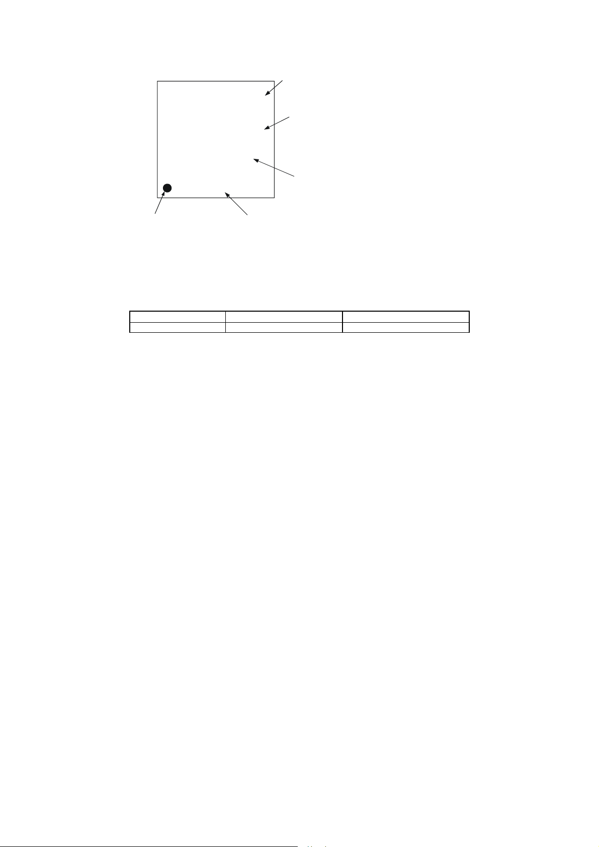
4.8 Mechanical - 32-QFN Package
PIN 1
Exposed
Centre
Pad
Corner tie
0
.
4
3
m
m
bar
DimensionsIn Millimeters
Symbol Minimum Nominal Maximum
A 0.70 - 0.95
A1 0.00 0.02 0.05
b 0.18 0.25 0.32
C - 0.20 REF D 4.90 5.00 5.10
Depending upon the IC assembly supplier, the package may
be slightly different from that depicted above. See the
magnified areas for the main difference between the ICs.
Dimension L1 represents terminal pull-back from the package
edge. Where terminal pull-back exists, only the upper half of
the lead is visible on the package edge due to half etching of
the leadframe.
The corner tie bar is connected internally to the exposed
central pad.
D2 3.05 - 3.65
E 4.90 5.00 5.10
E2 3.05 - 3.65
e-0.50-
L 0.30 0.40 0.50
y 0.00 - 0.075
L1 0.00 - 0.10
Note that there is no functional requirement for the large pad on the underside of this package to be
soldered. If the final application requires this area to be soldered for mechanical reasons, the pad to
which it is soldered must be isolated and contained under the footprint only.
lQ 16 QT1081_1R0.04_0307
Page 17
4.9 Part Marking
QRG Part
No.
QT1081
©QRG 1
YYWWG
run nr.
Pin 1
Identification
4.10 Moisture Sensitivity Level (MSL)
'run nr.' = 6 Digit Run Number
(depending upon the
supplier
QRG
Revision
Code
‘YY’ = Year of manufa ct u re
‘WW’ = Week of manufacture
‘G’ = Green/RoHS Compliant
or ‘XX’ dependin g up on th e
IC assembly supplier
, this line may not appear)
IC assembly
SpecificationsPeak Body TemperatureMSL Rating
IPC/JEDEC J-STD-020C260OCMSL3
lQ 17 QT1081_1R0.04_0307
Page 18

5 Datasheet Control
5.1 Changes
Changes this issue (datasheet rev 04)
Changes throughout to remove 48-SSOP package.
Section 5: new.
5.2 Numbering Convention
Part Number
Datasheet Issue Number
QT1081_MXN.nn_mmyy
Chip Revision
(Where M= Major chip revision,
N = Minor chip revision,
X = Prereleased Product
[or R = Released Product])
A minor chip revision (N) is defined as a revision change which does not affect product functionality or datasheet.
The value of N is only stated for released parts (R).
Datasheet Release Date;
(Where mm = Month, yy = Year)
lQ 18 QT1081_1R0.04_0307
Page 19

NOTES:
lQ 19 QT1081_1R0.04_0307
Page 20

lQ
Copyright © 2006-2007 QRG Ltd. All rights reserved
Patented and patents pending
Corporate Headquarters
1 Mitchell Point
Ensign Way, Hamble SO31 4RF
Great Britain
Tel: +44 (0)23 8056 5600 Fax: +44 (0)23 8045 3939
www.qprox.com
North America
651 Holiday Drive Bldg. 5 / 300
Pittsburgh, PA 15220 USA
Tel: 412-391-7367 Fax: 412-291-1015
The specifications set out in this document are subject to change without notice. All products sold and services supplied by QRG are subject to
QRG’s Terms and Conditions of sale and services. QRG patents, trademarks and Terms and Conditions can be found online at
http://www.qprox.com/about/legal.php. Numerous further patents are pending, one or more which may apply to this device or the applications
thereof.
QRG products are not suitable for medical (including lifesaving equipment), safety or mission critical applications or other similar purposes.
Except as expressly set out in QRG's Terms and Conditions, no licenses to patents or other intellectual property of QRG (express or implied)
are granted by QRG in connection with the sale of QRG products or provision of services. QRG will not be liable for customer product design
and customers are entirely responsible for their products and applications which incorporate QRG's products.
Development Team: John Dubery, Alan Bowens, Matthew Trend
 Loading...