

lQ QT1080
z 8 completely independent QT touch sensing fields
z Designed for low-power portable applications
z 100% autocal for life - no adjustments required
z Direct outputs - either encoded or ‘per key’
z Fully debounced results
z 2.8V ~ 5.0V single supply operation
z 45µA current typ @ 3V in 360ms LP mode
z AKS™ Adjacent Key Suppression
z Spread spectrum bursts for superior noise rejection
z Sync pin for excellent LF noise rejection
z 10ms ‘fast mode’ for use in slider applications
z Pb-free packages: 32-QFN and 48-SSOP
APPLICATIONS
MP3 players
Mobile phones
PC peripherals
Television controls
8 KEY QT
25
OUT_0
26
OUT_1
27
OUT_2
28
OUT_3
29
OUT_4
30
OUT_5
31
OUT_6
OUT_7
32
Pointing devices
Remote controls
OUCH
DETECT
24 23 222120 19 18 17
1
23456 78
SS
SYNC/LP
VSS
QT1080
32-QFN
VDD
/RST
™ S
SNS7K
SNS7
N.C.
OSC
SNS6K
SNS6
SNS0
SNS0K
ENSOR
SNS5K
SNS5
16
SNS4K
15
SNS4
14
SNS3K
13
SNS3
12
SNS2K
11
SNS2
10
SN1K
9
SNS1
IC
QT1080 charge-transfer (“QT’”) QTouch IC is a self-contained digital controller capable of detecting near-proximity or touch on up to 8
electrodes. It allows electrodes to project independent sense fields through any dielectric such as glass or plastic. This capability
coupled with its continuous self-calibration feature can lead to entirely new product concepts, adding high value to product designs. The
devices are designed specifically for human interfaces, like control panels, appliances, gaming devices, lighting controls, or anywhere a
mechanical switch or button may be found; they may also be used for some material sensing and control applications.
Each of the channels operates independently of the others, and each can be tuned for a unique sensitivity level by simply changing a
corresponding external Cs capacitor.
AKS™ Adjacent Key Suppression (patent pending) suppresses touch from weaker responding keys and allows only a dominant key to
detect, for example to solve the problem of large fingers on tightly spaced keys.
Spread spectrum burst technology provides superior noise rejection. These devices also have a SYNC/LP pin which allows for
synchronization with additional similar parts and/or to an external source to suppress interference, or, an LP (low power) mode which
conserves power.
By using the charge transfer principle, this device delivers a level of performance clearly superior to older technologies yet is highly
cost-effective.
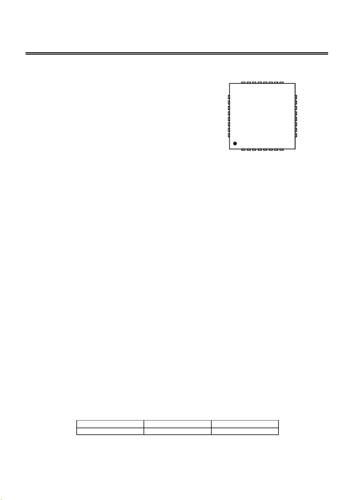
This part is available in both 32-QFN and 48-SSOP lead-free packages.
LQ
AVAILABLE OPTIONS
A
48-SSOP32-QFNT
QT1080-IS48GQT1080-ISG-40ºC to +85ºC
Copyright © 2004-2005 QRG Ltd
QT1080 R11.03/0905

1 - OVERVIEW
The QT1080 is an easy to use, 8 touch-key sensor IC based
on Quantum’s patented charge-transfer principles for robust
operation and ease of design. This device has many
advanced features which provide for reliable, trouble-free
operation over the life of the product.
Burst operation: The device operates in ‘burst mode’. Each
key is acquired using a burst of charge-transfer sensing
pulses whose count varies depending on the value of the
reference capacitor Cs and the load capacitance Cx. In LP
mode, the device sleeps in an ultra-low current state
between bursts to conserve power. The keys signals are
acquired using two successive bursts of pulses:
Burst A: Keys 0, 1, 4, 5
Burst B: Keys 2, 3, 6, 7
Bursts always operate in A-B sequence.
Self-calibration: On power-up, all 8 keys are self-calibrated
within 350 milliseconds (typical) to provide reliable operation
under almost any conditions.
Auto-recalibration: The device can time out and recalibrate
each key independently after a fixed interval of continuous
touch detection, so that the keys can never become ‘stuck
on’ due to foreign objects or other sudden influences. After
recalibration the key will continue to function normally. The
delay is selectable to be either 10s, 60s, or infinite
(disabled).
The device also auto-recalibrates a key when its signal
reflects a sufficient decrease in capacit ance. In this case the
device recalibrates after ~2 seconds so as to recover normal
operation quickly.
Drift compensation operates to correct the reference level
of each key slowly but automatically over time, to suppress
false detections caused by changes in temperature,
humidity, dirt and other environmental effects.
The drift compensation is asymmetric: in the increasing
capacitive load direction the device drifts more slowly than in
the decreasing direction. In the increasing direction, the rate
of compensation is 1 count of signal per 2 seconds; in the
opposing direction, it is 1 count every 500ms.
Detection Integrator (‘DI’) confirmation reduces the
effects of noise on the QT1080 outputs. The ‘detect
integrator’ mechanism requires consecutive detections over
a number of measurement bursts for a touch to be confirmed
and indicated on the outputs. In a like manner, the end of a
touch (loss of signal) has to be confirmed over a number of
measurement bursts. This process acts as a type of
‘debounce’ against noise.
In normal operation, both the start and end of a touch must
be confirmed for 6 measurement bursts. In a special ‘Fast
Detect‘ mode (available via jumper resistors), confirmation of
the start of a touch requires only 2 sequential detections, but
confirmation of the end of a touch is still 6 bursts.
Fast detect is only available when AKS is disabled.
Spread Spectrum operation: The bursts operate over a
spread of frequencies, so that external fields will have
minimal effect on key operation and emissions are very
weak. Spread spectrum operation works with the ‘detect
integrator’ (DI) mechanism to dramatically reduce the
probability of false detection due to noise.
Sync Mode: The QT1080 features a Sync mode to allow the
device to slave to an external signal source, such as a mains
signal (50/60Hz), to limit interference effects. This is
performed using the SYNC/LP pin. Sync mode operates by
triggering two sequential acquire bursts, in sequence A-B
from the Sync signal (see above); thus, each Sync pulse
causes all 8 keys to be acquired.
Low Power (LP) Mode: The device features an LP mode for
microamp levels of current drain with a slower response
time, to allow use in battery operated devices. On detection
of touch, the device automatically reverts to its normal mode
and asserts the DETECT pin active to wake up a host
controller. The device remains in normal, full acquire speed
mode until another pulse is seen on its SYNC/LP pin, upon
which it goes back to LP mode.
AKS™ Adjacent Key Suppression is a patent-pending
feature that can be enabled via jumper resistors. AKS works
to prevent multiple keys from responding to a single touch, a
common complaint about capacitive touch panels. This can
happen with closely spaced keys, or with control surfaces
that have water films on them.
AKS operates by comparing signal strengths from keys
within a group of keys to suppress touch detections from
those that have a weaker signal change than the dominant
one.
The QT1080 has two different AKS groupings of keys,
selectable via option resistors. These groupings are:
y AKS operates in two groups of 4 keys.
y AKS operates over all 8 keys.
These two modes allow the designer to provide AKS while
also providing for shift or function operations.
If AKS is disabled, all keys can operate simultaneously.
Outputs: There are two output modes: one per key, and
binary coded.
One per key outputs:
key. This mode has two output drive options, push-pull and
open-drain. The outputs can also be made either active-high
or active-low. These options are set via external
configuration resistors.
Binary coded outputs:
one possible key in detect. If more than one key is detecting,
only the first one touched will be indicated.
Simplified Mode: To reduce the need for option resistors,
the simplified operating mode places the part into fixed
settings with only the AKS feature being selectable. LP
mode is also possible in this configuration. Simplified mode
is suitable for most applications.
In this mode there is one output pin per
In this mode, 3 output lines encode for
lQ
2 QT1080 R11.03/0905

1.1 - Wiring
Table 1.1 Pinlist
32-QFN
Pin
5
-
48-SSOP
Pin
OscillatorIOSC374
38, 39, 40,
41, 42
I/OSNS0436
I/OSNS1458
I/OSNS24710
I/OSNS3112
I/OSNS4314
I/OSNS5516
I/OSNS6718
I/OSNS6K819
I/OSNS7920
11, 12, 13,
14, 15, 16
2123
‡
Pin Type
I CMOS input only
I/O CMOS I/O
O CMOS push-pull output
OD CMOS open drain output
O/OD CMOS push pull or open-drain output (option selected)
Pwr Power / ground
Sense pin and
option select
Sense pin and
option select
Sense pin and
option select
Sense pin and
option select
Sense pin and
option select
Sense pin and
option select
Sense pin and
option select
Sense pin and
mode select
Sense pin and mode
or option select
Out 2O/ODOUT_22727
Out 3O/ODOUT_32828
Resistor to Vdd and optional
spread spectrum RC network
To Cs0 and/or
option resistor
To Cs1 and/or
option resistor*
To Cs2 and/or
option resistor*
To Cs3 and/or
option resistor*
To Cs4 and/or
option resistor*
To Cs5 and/or
option resistor*
To Cs6 and/or
option resistor*
To Cs6 + Key and/or
mode resistor
†
To Cs7 and/or mode resistor
or option resistor*
Also, binary coded output 2
In binary coded mode, these
pins are clamped internally to
Vss
100K resistor to VssSpread spectrum driveSpread spectrumODSS331
†
If UnusedNotesFunctionTypeName
-Leave open--n/c34 -
VddActive low resetReset inputI/RST352
-+2.8 ~ +5.0VPowerPwrVdd363
-
-Leave open--n/c
Option resistor
OpenTo Cs0 + KeySense pinI/OSNS0K447
Open or
option resistor*
OpenTo Cs1 + KeySense pinI/OSNS1K469
Open or
option resistor*
OpenTo Cs2 + KeySense pinI/OSNS2K4811
Open or
option resistor*
OpenTo Cs3 + KeySense pinI/OSNS3K213
Open or
option resistor*
OpenTo Cs4 + KeySense pinI/OSNS4K415
Open or
option resistor*
OpenTo Cs5 + KeySense pinI/OSNS5K617
Open or
option resistor*
Open or
mode resistor
Open or mode
†
or option
resistor
resistor*
OpenTo Cs7 + KeySense pinI/OSN7K1021
-Leave open--n/c
-0VGroundPwrVss1722
-Leave open--n/c18, 19, 20 -
Vdd or VssRising edge sync or LP pulseSync In or LP InISYNC/LP
OpenActive = any key in detectDetect StatusO/ODDETECT2224
-Leave open--n/c23, 24 OpenAlso, binary coded output 0Out 0O/ODOUT_02525
OpenAlso, binary coded output 1Out 1O/ODOUT_12626
Open
Open
OpenOut 4O/ODOUT_42929
OpenOut 5O/ODOUT_53030
OpenOut 6O/ODOUT_63131
OpenOut 7O/ODOUT_73232
†
Notes
†
Mode resistor is required only in Simplified mode (see Figure 1.2)
* Option resistor is required only in Full Options mode (see Figure 1.1)
‡
Pin is either Sync or LP depending on options selected (functions SL_0, SL_1, see Figure 1.1)
lQ
3 QT1080 R11.03/0905
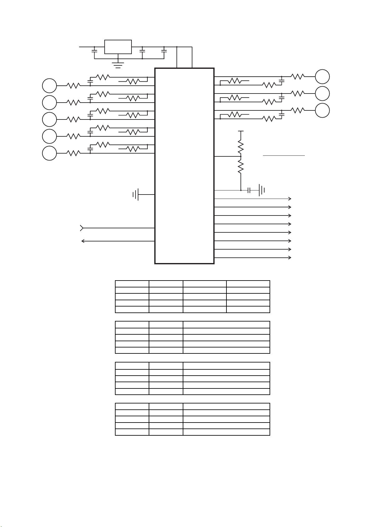
Figure 1.1 Connection Diagram - Full Options; Shown for 32-QFN Package
KEY 3
KEY 4
KEY 5
KEY 6
KEY 7
Vunreg
R
SNS3
10K
R
SNS4
10K
R
SNS5
10K
R
SNS6
R
SNS7
10K
10K
4.7nF
4.7nF
4.7nF
4.7nF
4.7nF
*4.7uF
C
S3
C
S4
C
S5
C
S6
C
S7
+2.8 ~ +5V
Voltage Reg
2.2K
R
S3
Vdd / Vss
2.2K
R
S4
Vdd / Vss
2.2K
R
S5
Vdd / Vss
2.2K
R
S6
Vdd / Vss
2.2K
R
S7
Vdd / Vss
MOD_1
POL
OUT_D
SL_0
SL_1
*4.7uF
VDD
*100nF
3
SNS3
SNS3K
SNS4
SNS4K
SNS5
SNS5K
SNS6
SNS6K
SNS7
SNS7K
VDD
12
1M
13
14
1M
15
16
1M
17
18
1M
19
20
1M
21
2
/RST
QT1080
*Note: One bypass cap to be tightly wired
between Vdd and Vss. Follow manufacturer’s
recommendations for input and output capacitors.
11
SNS2K
SNS2
SNS1K
SNS1
SNS0K
SNS0
OSC
10
9
8
7
6
4
MOD_0
1M
AKS_1
1M
AKS_0
1M
VDD
Rb1
Rb2
32-QFN
1
SS
OUT_7
OUT_6
OUT_5
OUT_4
OUT_3
OUT_2
OUT_1
OUT_0
32
31
30
29
28
27
26
25
SYNC or LP IN
DETECT OUT
22
23
24
VSS
SYNC/LP
DETECT
4.7nF
R
2.2K
2.2K
2.2K
S2
C
S2
4.7nF
R
S1
C
S1
4.7nF
R
S0
C
S0
Vdd / Vss
Vdd / Vss
Vdd / Vss
Recommended Rb1, Rb2 Values
Vdd Range Rb1 Rb2
2.8 ~ 3.59V 12K 22K
3.6 ~ 5V
15K 27K
100nF
R
SNS2
10K
R
SNS1
10K
R
SNS0
10K
OUT_7
OUT_6
OUT_5
OUT_4
OUT_3
OUT_2
OUT_1
OUT_0
OUT_0
KEY 2
KEY 1
KEY 0
Table 1.2
AKS / Fast-Detect Options
Table 1.3
Max On-Duration
Table 1.4
Polarity & Output
Table 1.5
SYNC/
LP Function
FAST-DETECTAKS MODEAKS_0AKS_1
OffOffVssVss
EnabledOffVddVss
OffOn, in 2 groupsVssVdd
OffOn, globalVddVdd
MAX ON-DURATION MODEMOD_0MOD_1
10 seconds (nom) to recalibrateVssVss
60 seconds (nom) to recalibrateVddVss
Infinite (disabled)VssVdd
(reserved)VddVdd
OUT_n, DETECT PIN MODEPOLOUT_D
Binary coded, active high, push-pullVssVss
Direct, active low, open-drainVddVss
Direct, active high, push-pullVssVdd
Direct, active low, push-pullVddVdd
SYNC/LP PIN MODESL_0SL_1
SyncVssVss
LP mode: 110ms nom response timeVddVss
LP mode: 200ms nom response timeVssVdd
LP mode: 360ms nom response timeVddVdd
lQ
4 QT1080 R11.03/0905
Figure 1.2 Connection Diagram - Simplified Mode; Shown for 32-QFN
SMR resistor installed between SNS6K and SNS7.
KEY 3
KEY 4
KEY 5
KEY 6
KEY 7
DETECT OUT
Vunreg
R
SNS3
10K
R
SNS4
10K
R
SNS5
10K
R
SNS6
10K
R
SNS7
10K
LP IN
4.7nF
4.7nF
4.7nF
4.7nF
4.7nF
*4.7uF
C
S3
C
S4
C
S5
C
S6
C
S7
+2.8 ~ +5V
Voltage Reg
R
S3
2.2K
R
S4
2.2K
R
S5
2.2K
R
S6
2.2K
R
S7
2.2K
SMR
*4.7uF
VDD
*100nF
3
SNS3
SNS3K
SNS4
SNS4K
SNS5
SNS5K
SNS6
SNS6K
SNS7
SNS7K
VDD
12
13
14
15
16
17
18
19
1M
20
21
2
/RST
QT1080
*Note: One bypass cap to be tightly wired
between Vdd and Vss. Follow manufacturer’s
recommendations for input and output capacitors.
SNS2K
SNS2
SNS1K
SNS1
SNS0K
SNS0
OSC
11
10
9
8
7
6
4
AKS_0
1M
Vdd / Vss
VDD
Rb1
Rb2
Recommended Rb1, Rb2 Values
4.7nF
R
S2
2.2K
4.7nF
R
S1
2.2K
4.7nF
R
S0
2.2K
Vdd Range Rb1 Rb2
2.8 ~ 3.59V 12K 22K
3.6 ~ 5V
R
10K
C
S2
R
10K
C
S1
R
10K
C
S0
15K 27K
SNS2
KEY 2
SNS1
KEY 1
SNS0
KEY 0
32-QFN
22
23
24
VSS
SYNC/LP
DETECT
SS
OUT_7
OUT_6
OUT_5
OUT_4
OUT_3
OUT_2
OUT_1
OUT_0
1
32
31
30
29
28
27
26
25
100nF
OUT_7
OUT_6
OUT_5
OUT_4
OUT_3
OUT_2
OUT_1
OUT_0
OUT_0
Table 1.6
AKS Resistor Options
Table 1.7
Functions in Simplified Mode
Output Drive,
SYNC/LP pin
Max on-duration delay
Detect Pin
Polarity
FAST-DETECTAKS MODEAKS_0
EnabledOffVss
OffOn, globalVdd
Direct outputs, push-pull, active high
200ms nom LP function; sync not available
60 seconds (nom)
Active high on any detect
lQ
5 QT1080 R11.03/0905

2 DEVICE OPERATION
2.1 Startup Time
After a reset or power-up event, the device requires 350ms
to initialize, calibrate, and start operating normally. Keys will
work properly once all keys have been calibrated after reset.
2.2 Option Resistors
The option resistors are read on power-up only. There are
two primary option mode configurations: full, and simplified.
In full options mode, eight 1M✡ option resistors are required
as shown in Figure 1.1. All eight resistors are mandatory.
To obtain simplified mode, a 1M✡ resistor should be
connected from SNS6K to SNS7. In simplified mode, only
one additional 1M✡ option resistor is required for the AKS
feature (Figure 1.2).
Note that the presence and connection of option resistors
will affect the required values of Cs; this effect will be
especially noticeable if the Cs values are under 22nF. Cs
values should be adjusted for optimal sensitivity after the
option resistors are connected.
2.3 OUT Pins - Direct Mode
Direct output mode is selected via option resistors, as shown
in Table 1.4.
In this mode, there is one output for each key; each is active
when there is a touch confirmed on the corresponding
electrode. Unused OUT pins should simply be left open.
If AKS is off, it is possible for all OUT pins to be active at the
same time.
Circuit of Figure 1.1: OUT polarity and drive are governed
by the resistor connections to Vdd or Vss according to Table
1.4. The drive can be either push-pull or open-drain, active
low or high.
Circuit of Figure 1.2: In this simplified circuit, the OUT pins
are active high, push-pull only.
2.4 OUT Pins - Binary Coded Mode
Binary code mode is selected via option resistors, as shown
in Table 1.4.
In this mode, a key detection is registered as a binary code
on pins OUT_2, OUT_1 and OUT_0, with possible values
from 000 to 111. In practice, 4 lines are required to read the
code, unless key 0 is not implemented: the output code 000
can mean either ‘nothing detecting’ or ‘key 0 is detecting’.
The 4th required line (if all 8 keys are implemented) is the
DETECT signal, which is active-high when any key is active.
The first key touched always wins and shows its output.
Keys that come afterwards are hidden until the currently
reported key has stopped detecting, in which case the code
will change to the latent key.
This mode is useful to reduce the number of connections to
a host controller, at the expense of being able to only report
one active key at a time. Note that in global AKS mode
(Section 2.7), only one key can report active at a time
anyway.
Circuit of Figure 1.1: OUT polarity and drive can only be
push-pull and active high.
Circuit of Figure 1.2: Binary coded not available.
2.5 DETECT Pin
DETECT represents the functional logical-OR of all eight
keys. DETECT can be used to wake up a battery-operated
product upon human touch.
DETECT is also required to indicate to a host when the
binary coded output pins (in that mode) are showing an
active key. While DETECT is active, the binary coded
outputs should be read at least twice along with DETECT to
make sure that the code was not transitioning between
states, to prevent a false reading.
The output polarity and drive of DETECT are governed
according to Table 1.4.
2.6 SYNC/LP Pin
The SYNC / LP pin function is configured according to the
SL_0 and SL_1 resistor connections to either Vdd or Vss,
according to the Table 1.5.
Sync mode: Sync allows the designer to synchronize
acquire bursts to an external signal source, such as mains
frequency (50/60 Hz) to suppress interference. It can also be
used to synchronize two QT parts which operate near each
other, so that they will not cross-interfere if two or more of
the keys (or associated wiring) of the two parts are near
each other.
The SYNC input of the QT1080 is positive pulse triggered. If
the SYNC input does not change, the device will free-run at
its own rate after ~150ms.
A trigger pulse on SYNC will cause the device to fire two
acquire bursts in A-B sequence:
Burst A: Keys 0, 1, 4, 5
Burst B: Keys 2, 3, 6, 7
Low Power LP Mode: This allows the device to enter a slow
mode with very low power consumption, in one of three
response time settings - 110ms, 200ms, and 360ms
nominal.
LP mode is entered by a positive, >150µs trigger pulse on
the SYNC/LP pin. Once the LP pulse is detected , the device
will enter and remain in this microamp mode until it senses
and confirms a touch, upon which it will switch back to
normal (full speed) mode on its own, with a response time of
30ms typical (burst length dependent). The device will go
back to LP mode again if SYNC/LP is held high, or after
another LP pulse is received.
The response time setting is determined by option resistors
SL_1 and SL_0; see Table 1.5. Slower response times result
in lower power drain.
The SYNC/LP pulse should be >150µs in duration.
If the SYNC/LP pin is held high permanently, the device will
go into normal mode during a key touch, and return to
low-current mode when the detection ceases.
If the SYNC/LP pin is held low constantly, the device will
simply remain in normal mode (25ms typical response time)
continuously.
2.7 AKS™ Function Pins
The QT1080 features an adjacent key suppression (AKS™)
function with 2 modes. Option resistors act to set this feature
according to Tables 1.2 and 1.6. AKS can also be disabled,
allowing any combination of keys to become active at the
same time. When operating, the modes are:
lQ
6 QT1080 R11.03/0905

Global: AKS functions operates across all 8 keys. This
means that only one key can be active at any one time.
Groups: AKS functions among two groups of four keys:
0-1-4-5 and 2-3-6-7. This means that up to 2 keys can be
active at any one time.
In Group mode, keys in one group have no AKS interaction
with keys in the other group.
Note that in Fast Detect mode, AKS can only be off.
The other option features are fixed as follows:
OUT_n, DETECT Pins: Push-pull, active high, direct
outputs
SYNC/LP Function: LP mode, ~200ms response time
Max On-Duration: 60 seconds
See also Tables 1.6 and 1.7.
2.8 MOD_0, MOD_1 Inputs
In full option mode, MOD_0 and MOD_1 resistors are used
to set the ‘Max On-Duration’ recalibration timeouts. If a key
becomes stuck on for a lengthy duration of time, this feature
will cause an automatic recalibration event of that specific
key only once the specified on-time has been exceeded.
Settings of 10s, 60s, and infinite are available.
The Max On-Duration feature operates on a key-by-key
basis; when one key is stuck on, its recalibration has no
effect on other keys.
The logic combination on the MOD option pins sets the
timeout delay; see Table 1.3.
Simplified mode MOD timing: In simplified mode, the max
on-duration is fixed at 60 seconds.
2.9 Fast Detect Mode
In many applications, it is desirable to sense touch at high
speed. Examples include scrolling ‘slider’ strips or ‘Off’
buttons. It is possible to place the device into a ‘Fast Detect’
mode that usually requires under 10ms to respond. This is
accomplished internally by setting the Detect Integrator to
only 2 counts, i.e. only two successive detections are
required to detect touch.
In LP mode, ‘Fast’ detection will not speed up the initial
delay (which could be up to 360ms nominal depending on
the option setting), however once a key is detected the
device is forced back into normal speed mode; it will remain
in this faster mode until another LP pulse is received.
When used in a ‘slider’ application, it is normally desirable to
run the keys without AKS.
In both normal and ‘Fast’ modes, the time required to
process a key release is the same: it takes 6 sequential
confirmations of non-detection to turn a key off.
Fast Detect mode can be enabled as shown in Tables 1.2
and 1.6.
2.10 Simplified Mode
A simplified operating mode which does not require the
majority of option resistors is available. This mode is set by
connecting a resistor labelled SMR between pins SNS6K
and SNS7; see Figure 1.2.
In this mode there is only one option possible - AKS enable
or disable. When AKS is disabled, Fast Detect mode is
enabled; when AKS is enabled, Fast Detect mode is off.
AKS in this mode is Global only (i.e. operates across all
functioning keys).
2.11 Unused Keys
Unused keys should be disabled by removing the
corresponding Cs, Rs, and Rsns components and
connecting SNS pins as shown in the ‘Unused’ column of
Table 1.1. Unused keys are ignored and do not factor into
the AKS function (Section 2.7).
3 - DESIGN NOTES
3.1 Oscillator Frequency
The QT1080’s internal oscillator runs from an external
resistor network connected to the OSC and SS pins as
shown in Figures 1.1 and 1.2 to achieve spread spectrum
operation. If spread spectrum mode is not required, the OSC
pin should simply be connected to Vdd with an 18K ohm 1%
resistor.
Under different Vdd voltage conditions the resistor network
(or the solitary 18K ohm resistor) might require minor
adjustment to obtain the specified burst center frequency.
The network should be adjusted slightly so that the positive
pulses on any key are approximately 2µs wide in the ‘solitary
18K resistor’ mode, or 2.15µs wide at the beginning of a
burst with the recommended spread spectrum circuit (see
next section).
In practice, the pulse width has little effect on circuit
performance if it varies in the range from 1.5µs to 2.5µs. The
only effects will be seen in non-LP mode, as proportional
variations in Max On-Duration times and response times.
3.2 Spread Spectrum Circuit
The QT1080 offers the ability to spectrally spread its
frequency of operation to heavily reduce susceptibility to
external noise sources and to limit RF emissions. The SS pin
is used to modulate an external passive RC netw ork that
modulates the OSC pin. OSC is the main oscillator current
input. The circuit is shown in both Figures 1.1 and 1.2.
The resistors Rb1 and Rb2 should be changed depending
on Vdd. As shown in Figures 1.1 and 1.2, two sets of values
are recommended for these resistors depending on Vdd.
The power curves in Section 4.6 also show the effect of
these resistors.
The circuit can be eliminated if it is not desired by simply
using an 18K ohm resistor from OSC to Vdd to drive the
oscillator, and connecting SS to Vss with a 100K ohm
resistor. This mode consumes significantly less current than
spread spectrum mode.
The spread-spectrum RC network might need to be modified
slightly if the burst lengths are particularly long. Vdd
variations can shift the center frequency and spread slightly.
The sawtooth waveform observed on SS should reach a
crest height as follows:
Vdd >= 3.6V: 17% of Vdd
Vdd < 3.6V: 20% of Vdd
lQ
7 QT1080 R11.03/0905

The 100nF capacitor connected to SS (Figures 1.1 and 1.2)
should be adjusted so that the waveform approximates the
above amplitude, +/-10%, during normal operation in the
target circuit. If this is done, the circuit will give a spectral
modulation of 12-15%.
3.3 Cs Sample Capacitors; Sensitivity
The Cs sample capacitors accumulate the charge from the
key electrodes and determine sensitivity. Higher values of
Cs make the corresponding sensing channel more sensitive.
The values of Cs can differ for each channel, permitting
differences in sensitivity from key to key or to balance
unequal sensitivities. Unequal sensitivities can occur due to
key size and placement differences and stray wiring
capacitances. More stray capacitance on a sense trace will
desensitize the corresponding key; increasing the Cs for that
key will compensate for the loss of sensitivity.
The Cs capacitors can be virtually any plastic film or low to
medium-K ceramic capacitor. The ‘normal’ Cs range is 2.2nF
to 50nF depending on the sensitivity required; larger values
of Cs require better quality to ensure reliable sensing.
Acceptable capacitor types for most uses include PPS film,
polypropylene film, and NP0 and X7R ceramics. Lower
grades than X7R are not advised.
The required values of Cs can be noticeably affected by the
presence and connection of the option resistors (see Section
2.2).
3.4 Power Supply
The power supply can range from 2.8 to 5.0 volts. If this
fluctuates slowly with temperature, the device will track and
compensate for these changes automatically with only minor
changes in sensitivity. If the supply voltage drifts or shifts
quickly, the drift compensation mechanism will not be able to
keep up, causing sensitivity anomalies or false detections.
The power supply should be locally regulated using a
3-terminal device, to between 2.8V and 5.0V. If the supply is
shared with another electronic system, care should be taken
to ensure that the supply is free of digital spikes, sags, and
surges which can cause adverse effects.
For proper operation a 0.1µF or greater bypass capacitor
must be used between Vdd and Vss; the bypass capacitor
should be routed with very short tracks to the device’s Vss
and Vdd pins.
3.5 PCB Layout and Construction
Please refer to Quantum application note AN-KD02 for
information related to layout and construction matters.
lQ
8 QT1080 R11.03/0905

4 - SPECIFICATIONS
4.1 Absolute Maximum Specifications
Operating temperature, Ta.............................................................................................. -40 ~ +85ºC
Storage temp, Ts................................................................................................... -50ºC ~ +125ºC
Vdd................................................................................................................... -0.3 ~ +6.0V
Max continuous pin current, any control or drive pin............................................................................ ±20mA
Short circuit duration to ground or Vdd, any pin................................................................................. infinite
Voltage forced onto any pin..................................................................................-0.3V ~ (Vdd + 0.3) Volts
4.2 Recommended Operating Conditions
Operating temperature, Ta.............................................................................................. -40 ~ +85ºC
DD
...................................................................................................................+2.8 ~ +5.0V
V
Short-term supply ripple+noise...............................................................................................±5mV/s
Long-term supply stability...................................................................................................±100mV
Cs range............................................................................................................ 2.2nF ~ 100nF
Cx range................................................................................................................. 0 ~ 50pF
4.3 AC Specifications
Vdd = 5.0, Ta = recommended, Cx = 5pF, Cs = 4.7nF; circuit of Figure 1.1
NotesUnitsMaxTypMinDescriptionParameter
ms150Recalibration timeTrc
kHz132Burst center frequencyFc
Total deviation%15Burst modulation, percentFm
µs2Sample pulse durationTpc
ms350Startup time from cold startTsu
Both bursts togetherms3.4Burst durationTbd
ms10Response time - Fast modeTdf
ms25Response time - Normal modeTdn
200ms LP settingms200Response time - LP modeTdl
End of touchms25Release time - all modesTdr
4.4 DC Specifications
Vdd = 5.0, Ta = recommended, Cx = 5pF, Cs = 4.7nF; circuit of Figure 1.1 unless noted
DDN
DDL
DDS
IL
HL
OL
OH
IL
R
Supply current, normal mode*I
2.7
2.2
1.8
1.5
1.3
*No spread spectrum circuit; Rosc = 18K ohms
4.5 Signal Processing
Vdd = 5.0, Ta = recommended, Cx = 5pF, Cs = 4.7nF
NotesUnitsValueDescription
Threshold for increase in Cx loadcounts10Detection threshold
counts2Detection hysteresis
Threshold for decrease of Cx loadcounts6Anti-detection threshold
Time to recalibrate if Cx load has exceeded anti-detection thresholdsecs2Anti-detection recalibration delay
Must be consecutive or detection failssamples6Detect Integrator filter, normal mode
Must be consecutive or detection failssamples2Detect Integrator filter, ‘fast’ mode
Option pin selectedsecs10, 60, ∞Max On-Duration
Towards increasing Cx loadms/level2,000Normal drift compensation rate
Towards decreasing Cx loadms/level500Anti drift compensation rate
NotesUnitsMaxTypMinDescriptionParameter
mA84.5
@ Vdd = 5.0
@ Vdd = 4.0
@ Vdd = 3.6
@ Vdd = 3.3
@ Vdd = 3.0
@ Vdd = 2.8
@ Vdd = 3.0; 360ms LP modeµA45Supply current, LP mode*I
Req’d for startup, w/o external reset cktV/s100Supply turn-on slopeV
V0.7Low input logic levelV
V3.5High input logic levelV
7mA sinkV0.5Low output voltageV
2.5mA sourceVVdd-0.5High output voltageV
µA±1Input leakage currentI
bits8Acquisition resolutionA
lQ
9 QT1080 R11.03/0905

4.6 Idd Curves
Cx = 5pF, Cs = 4.7nF, Ta = 20oC, Spread spectrum circuit of Fig. 1.1.
QT1080 Idd (norm al m ode) m A
5.0
4.0
3.0
2.0
Idd(mA)
1.0
Rb1=12K
Rb2=22K
0.0
2.5 3 3.5 4 4.5 5 5.5
QT1080 Idd (200m s re s pons e) µA
400
300
200
Idd(µA)
100
Rb1=12K
Rb2=22K
0
2.533.544.555.5
Vdd(V)
Vdd(V)
Rb1=15K
Rb2=27K
Rb1=15K
Rb2=27K
QT1080 Idd (110m s re s po ns e ) µA
500
400
300
200
Idd(µA)
100
300
250
200
150
Idd(µA)
100
Rb1=12K
Rb2=22K
0
2.533.544.555.5
QT1080 Idd (360m s re s po ns e ) µA
Rb1=12K
Rb2=22K
50
0
2.533.544.555.5
Vdd(V)
Vdd(V)
Rb1=15K
Rb2=27K
Rb1=15K
Rb2=27K
Cx = 5pF, Cs = 4.7nF, Ta = 20oC, Rosc = 18K ohms; no spread spectrum circuit
QT1080 Idd (n or m al m ode) mA
5.0
4.0
3.0
2.0
Idd(mA)
1.0
0.0
2.5 3 3.5 4 4.5 5 5.5
QT1080 Idd (200m s re sponse) µA
250
200
150
100
Idd(µA)
50
Vdd(V)
QT1080 Idd (110m s re sponse) µA
400
300
200
Idd(µA)
100
0
2.5 3 3.5 4 4.5 5 5.5
QT1080 Idd (360m s re sponse) µA
125
100
75
50
Idd(µA)
25
Vdd(V)
0
2.5 3 3.5 4 4.5 5 5.5
lQ
Vdd(V)
0
2.533.544.555.5
Vdd(V)
10 QT1080 R11.03/0905

4.7 LP Mode Typical Response Times
Response Time vs Vdd - 110ms Setting
130
125
120
115
110
105
100
95
Actu al Re spo ns e Time, ms
90
2.5 3 3.5 4 4. 5 5 5.5
Vdd
Response Time vs Vdd - 360ms Setting
430
410
390
370
350
330
310
Actu al Re spo ns e Time, ms
290
2.5 3 3.5 4 4.5 5 5.5
Vdd
Response Time vs Vdd - 200ms Setting
240
230
220
210
200
190
180
170
Actu al Re spo ns e Time, ms
160
2.5 3 3.5 4 4.5 5 5.5
Vdd
lQ
11 QT1080 R11.03/0905

4.8 Mechanical - 32-QFN Package
A
PIN 1
C
Min Nom.
A
0.00
A1
A2
A3
B
C
0.20
D
0.30
E
3.35
F
3.35
G
e
ll dimensions i n millimetres
0.01
0.65
0.20 Ref.
5.00
5.00
0.25
0.40
3.50
3.50
0.50 bsc
B
G
D
Max
0.90
0.05
0.70
A2
0.32
0.50
3.65
3.65
A
A1
F
e
E
A3
Note that there is no functional requirement for the large pad on the underside of this package to be
soldered. If the final application requires this area to be soldered for mechanical reasons, the pad to
which it is soldered to must be isolated and contained under the footprint only.
4.9 Mechanical - 48-SSOP Package
A
C
G
D
E
Min
Max
B
F
All dimensions in millimeters
2.160.207.3910.03
0.64
Typ
J
H
a
aJHGFEDCBA
0.640.1015.570.10
0.890.3016.180.252.510.307.5910.67
o
0
o
8
lQ
12 QT1080 R11.03/0905

4.10 Part Marking
32-QFN 48-SSOP
Pin 48
DIMPLE
Pin 32
QT1080
©QRG 11
<datecode>
Pin 1
DIMPLE
Pin 1
QT1080-IS48G
© QRG 0803 R11
QProx
TM
<datecode>
lQ
13 QT1080 R11.03/0905

lQ
Copyright © 2005 QRG Ltd. All rights reserved
Patented and patents pending
Corporate Headquarters
Ensign Way, Hamble SO31 4RF
Tel: +44 (0)23 8056 5600 Fax: +44 (0)23 8045 3939
1 Mitchell Point
Great Britain
www.qprox.com
North America
651 Holiday Drive Bldg. 5 / 300
Pittsburgh, PA 15220 USA
Tel: 412-391-7367 Fax: 412-291-1015
This device covered under one or more of the following United States and corresponding international patents: 5,730,165, 6,288,707,
6,377,009, 6,452,514, 6,457,355, 6,466,036, 6,535,200. Numerous further patents are pending which may apply to this device or the
applications thereof.
The specifications set out in this document are subject to change without notice. All products sold and services supplied by QRG are
subject to our Terms and Conditions of sale and supply of services which are available online at www.qprox.com
every order acknowledgment. QProx, QTouch, QMatrix, QLevel, QSlide, QWheel, AKS are trademarks of QRG. QRG products are not
suitable for medical (including lifesaving equipment), safety or mission critical applications or other similar purposes. Except as expressly
set out in QRG's Terms and Conditions, no licenses to patents or other intellectual property of QRG (express or implied) are granted by
QRG in connection with the sale of QRG products or provision of QRG services. QRG will not be liable for customer product design and
customers are entirely responsible for their products and applications which incorporate QRG's products.
Development Team: John Dubery, Alan Bowens, Matthew Trend
and are supplied with
 Loading...