

Page 1

Q200
Series™
Intelligent Disk Drives
Technical Reference Manual
For Q250, Q280
Disk Drives
Page 2

Q200
SERIES
tm
INTELLIGENT DISK DRIVES
Q250jQ280
DISK
DRIVES
Technical
Publication
Reference
No.
REV
A
Manual
81-45528
Page 3

PREFACE
This
the
technicians
integrating
Quantum
products
or
Additional
following~manuals:
Publication
Quantum
Quantum
ANSI
Quantum
Representative,
spare
Publication
manual
Q250
contains
and
and
them
reserves
without
improvements
information
No.
81-45233
81-45416
X3.131-1986
publications
parts.
No
Q280
engineers
the
in
or
81-45528
rigid
into
incurring
units
may
technical
disk
evaluating
systems.
right
to
any
previously
on
the
Title
Q250/Q280
Q200
Small
may
be
Series
Computer
be
ordered
Rev.
reference
drives.
make
changes
obligation
Q250
Disk
and
Drives.
Programmer's
System
requested
from
KL587
UL/CSA/VDE
information
Information
or
maintaining
to
sold
or
Q280
Interface
from
Quantum
and/or
incorporate
shipped.
is
given
OEM
Manual
Manual
your
Quantum
in
describing
is
intended
the
drives,
improvements
such
in
the
(SCSI)
Sales
the
same
manner
for
or
to
its
changes
as
CSA
certification
VDE
Model
material
Q250
and
shipment.
~arranty
and
representative.
Quantum
The
and
u.S.
service
product
is
the
Patents
Copyright
Q200
AIRLOCK
Printed
Series
is
in
UL
recognition
certification
and
Q280
workmanship
The
warranty
further
center
described
subject
are
1987
Quantum
and
a
registered
DisCache
U.S.A.
granted
disk
details
All
requests
herein
of
allowed
expected
granted
under
granted
WARRANTY
drives
for
a
period
includes
can
for
in
your
area.
PATENTS
is
pending
to
issue
Corporation.
are
trademarks
trademark
under
File
per
are
warranted
parts
be
obtained
service
covered
in
All
of
Quantum
Nos.
File
of
one
and
by
patent
1987.
rights
of
File
No.
LR496896-8
No.
11342-3250-1002
against
year
labor.
from
should
u.S.
be
Patent
applications
reserved.
Quantum
Corporation.
E78016
and
defects
from
your
This
date
is
Quantum
directed
No.
Corporation.
LR496896-11
in
of
a
limited
sales
to
the
4,538,193,
from
which
ii
Page 4

PREFACE
TAB
L E o F
CON
TEN
T S
. .
ii
SECTION
1.1
1.2
Features
Logic
SECTION
2.1
Head
2.1.1
2.1.2
2.1.3
2.1.4
2.1.S
2.1.6
2.1.7
2.2
Drive
2.2.
2.2.2
2.2.3
2.2.4
2.2.S
2.2.6
2.2.7
2.2.8
2.3
PCB
2.3.1
2.3.2
2.3.3
2.3.4
2.3.S
2.3.6
2.3.7
2.3.8
2.3.9
2.3.10
2.4
2.S
2.6
Power-Up
Read
write
1.
INTRODUCTION .
. . . . . .
Conventions
2.
PRINCIPLES
Disk
Assembly
Base
Disk
Rotary
Headstack
Automatic
DC
Drive
Air
Electronics.
1
Disk
Simplified
SCSI
SCSI
SCSI
Power
Shorting
Flex
Functional
Power-On-Reset
Motor
Electronic
S080
Servo
Actuator
Read/Write
FYLO
DICEY
Microprocessor
Sequence/Recalibration.
Command
Command
..
casting
Stack
Assembly.
positioner
Assembly.
Actuator
Motor.
Filtration.
Format
Explanation--Block
Bus
Physical
Bus
Signal
Bus
Timing.
Requirements.
Plug
Circuit
Elements.
Control
Return
SCSI
Bus
Control,
Positioning
Circuit.
Timing
Data
Controller
Controller
Sequence.
Sequence.
OF
OPERATION
(HDA)
. . . . . .
Assembly.
..
. . .
. . . .
Assembly
(Actuator)
. . . . . . . . . .
Lock
(AIRLOCK)
. . . . .
...
.
..
. .
.
..............
. . . . . . . . .
Interface.
Descriptions
.
..
. . .
Options.
............
......
..
.
....................
.
..
(POR)
and
Circuit
Spring.
Controller.
AMC
and
...............
Servo
.
Warm
. . .
. . .
AGC.
circuit.
. . . . . . . . . . . .
IC,
and
IC.
and
EPROM
. . . . . . . .
.
..
.
..
..
.........
.........
.........
..
Diagram
......
...........
...........
Reset
..
. . .
.
..
xtal
........
.........
.
..........
...........
. . .
. . . . . . . .
. . . . . . . .
.
......
.
......
.......
.......
.......
.......
.
......
. .
........
.
.....
......
..
.
.....
..
..
Oscillators
..
......
.
.
1-1
1-1
1-2
2-1
2-1
2-1
2-2
2-2
2-2
2-2
2-2
2-3
2-4
2-4
2-4
2-8
2-10
2-11
2-14
2-16
2-19
2-19
2-19
2-20
2-21
2-21
2-23
2-27
2-27
2-29
2-30
2-32
2-32
2-33
2-33
SECTION
3.
ENGINEERING
DRAWINGS
.
iii
3-1
.
Page 5

SECTION
4.
APPLICATIONS . .
. . . . . .
4-1
4.1
4.2
4.3
Special
4.1.1
4.1.2
Errors
4 • 2 • 1
4.2.2
4.2.3
4.2.4
Grounding,
SECTION
5.1
5.2
5.3
5.4
5.5
Maintenance
Level
Level
Connector
PCB
5.5.1
5.5.2
5.5.3
SECTION
6.1
6.2
Spare
Reference
Considerations.
-REQ/-ACK
Hints
and
Errors.
Allocating
Creating
Updating
5.
MAINTENANCE.
1
Maintenance.
2
Maintenance.
Waveforms
Special
Techniques
Test
6.
PARTS
Parts
Handshake.
for
Software
Media
Defects.
. . . . . . . . . . . . . .
Replacement
the
the
Electrostatic
Precautions.
Maintenance.
and
Techniques.
Test
and
Connector
LISTS
List
Parts
...
....
List(s)
. . . . .
Driver
writers
. . . . . . . .
Sectors.
Defect
Drive
Lists.
Using
the
Discharges,
. .
. . . . . . . . .
. . . . . . . . .
. . .
. . . .
..
. . . . . . . .
Equipment
Waveform
J5
Signals.
...............
Descriptions
.
.
..
..
..
.
. . . . . .
Defect
and
Lists
EMI
..
..
............
.
.........
........
. . . . . .
.
......
...
.......
.....
. .
.
.....
..
..
....
.
....
.
...
...
...
..
. •
.•
..
. .
4-1
4-1
4-3
4-5
4 - 5
4-6
4-8
4-9
4-10
5-1
5-1
5-1
5-2
5-2
5-2
5-2
5-3
5-4
6-1
6-1
6-2
iv
Page 6

LIS
T
o F
FIG
U
RES
2-1
2-2
2-3
2-4
2-5
2-6
2-7
2-8
2-9
2-10
2-11
2-12
2-13
2-14
2-15
2-16
2-17
3-1
3-2
3-3
3-4
3-5
3-6
3-7
3-8
3-9
3-10
3-11
3-12
4-1
4-2
4-3
4-4
4-5
Exploded
Inside
Disk
Electronics
J1
SCSI
SCSI
Drive
General
Connector
5080
5080
Servo
Read
DICEY
Power-Up
Read
write
Printed
Schematic,
Schematic,
Schematic,
Printed
Schematic,
Schematic,
Schematic,
Printed
Schematic,
Schematic,
Schematic,
-REQ/-ACK
Buffer
In-Line
In-Line
Sparing
View
Format:
Connector.
Bus.
Bus
Startup
PCB
Conceptual
Interface
AMC
Circuit
Block
Command
Command
Circuit
Circuit
Circuit
Full
Sparing
Sparing
of
View
Timing
Locations
Sequence.
Handshake.
. . . . . .
of
Drive,
Wedges,
Block
. . . . . .
Typical
Current
Layout;
and
ADC
Waveforms
Diagram.
Sequence.
Sequence
PCB-7,
PCB-7,
PCB-7,
PCB-8,
PCB-8,
PCB-8,
PCB-9,
PCB-9,
PCB-9,
and
Field-Found
Showing
Sectors,
Diagram
Circuit
Diagram
Profile
Plug,
Block
Diagram
Circuit
. . . . .
.. ..
Board
Board
Board
Empty
of
Overflow
Parts
Sheet
Sheet
Sheet
Parts
Sheet
Sheet
Sheet
Parts
Sheet
Sheet
Sheet
Q250/Q280
Ratios.
Defective
..
Air
..
..
of
. . . . • . . . . . . . . . . . .
Terminator
Diagram.
. . . . . . .
Waveforms.
. . . . . . . . .
. .
..
. . . . .
Locations
1
· ·
2
· · · · · · · ·
3
· · · ·
Locations
1
·
2
· · ·
3
·
·
Locations
1
·
2
·
3
· · ·
Sectors.
of
Defective
Defective
......
Filtration.
and
Tracks.
............
.....
a
Signal
. . . .
. . . .
..
. . . . .
...
· ·
· · · · · ·
·
·
· · · ·
·
Line
..
and
.........
· . . . . . . . . 2
...
.
..
.
(PCB-7)
· ·
·
· · · ·
(PCB-8)
·
· ·
·
· ·
(PCB-9)
·
. . . . . .
. . . . . . . .
.....
.......
......
· . . . . . . .
· .
..
· . . .
· . . . . .
· . . . . .
· .
..
· . . . . . .
·
· ·
·
·
· ·
· ·
· · ·
·
· · · ·
· · · ·
·
·
· ·
· ·
·
· · ·
· · · · · · ·
· ·
·
Target
. . . . . . . . . . . . . .
Sectors.
· ·
Sends
. .
..
Sectors
. . . . . . . .
Data
·
·
. .
.
...
. . . . . .
. .
..
.
·
·
·
·
·
·
· ·
·
·
·
·
·
·
2-1
2-3
2-5
2-6
2-9
2-10
2-13
2-16
2-17
-2
2-22
2-25
2-28
2-31
2-34
2-35
2-36
3-2
3-3
3-4
3-5
3-6
3-7
3-8
3-9
3-10
3-11
3-12
3-13
4-2
4-3
4-7
4-7
4-8
2
5-1
5-2
5-3
Test
Test
Test
Waveforms(1)
Waveforms(2)
Waveforms(3)
v
· . . . .
· .
· . . . . .
5-6
5-7
5-8
Page 7

2-1
2-2
2-3
J1
Pin
Assignments.
DC
Power
Requirements
Microprocessors
LIS
and
T o F
. . . .
Buffer
.
.....
RAM.
TAB
..
. . . . .
.
L E S
...
. . . • . •
· • •
.
2-9
2-15
2-32
4-1
5-1
Available
Test
Connector
Spare
and
J5
Defective
Signals
. .
Sectors
.
· . .
· . •
4-8
5-5
vi
Page 8

1.1
Features
Q250
System
and
Interface
plug-in
(PCB).
electronics
and
actuator
the
flex
The
following
throughput:
o
o
o
o
Q280
EPROM
These
except
rotor
circuit
Seeks
processed
14
KByte
and
Optional
(See
concerning
Cylinder
accessing
drives
(SCSI)
IC,
both
drives
the
are
inside
features
are
FIFO
from
the
DisCache
the
Q200
and
feature
on-board,
controllers,
models
require
spindle
use
no
motor,
contained
the
sealed
of
the
Q250/Q280
initiated
immediately--other
simultaneously.
data
SCSI
buffer
bus
increases
Series
this
data
option.)
head
skewing
sequentially
ANSI-standard,
and,
the
same
operational
headstack,
on
the
PCB. A
assembly.
drives
balances
as
well
as
data
Programmers
scheme
across
with
the
printed
adjustments.
single
enable
the
to
and
buffer
Manual
minimizes
cylinder
Small
exception
circuit
flex
circuit,
IC
high
commands
transfer
from
size
for
the
to
details
latency
boundaries.
Computer
board
All
is
mounted
data
are
of
drive.
60
of
a
heads,
data
to
KBytes.
when
on
o
o
Defect
Multiple
to
o RLL
on
management
2
Kbytes.
1,7
the
disks.
scheme
block
transfer
(run-length-Iimited)
minimizes
of
up
to
encoding
seeks
64K-1
to
spare
blocks,
increases
each
data
sectors.
with
density
up
1-1
Page 9

SCSI
commands
management,
Programmable
initially
defective
to
reformat,
correcting
be
handled
of
17
bits,
relieve
error
options
and
throughout
sectors
(2)
code
in
the
or
correction,
can
data
(ECC) ,
host
detect
the
host
allow
the
be
automatically
can
be
or
computer.
three
users
product's
corrected
(3)
burst
system
and
flexible
all
of
physical
life.
reassigned
with
error
The
ECC
errors
many
tasks,
sector
ways
For
a
Reed-Solomon
detection
can
correct
of
17
addressing.
to
handle
example,
without
and
bits
such
correction
one
each.
as
defect
defects
(1)
the
error
burst
need
can
error
Q200
Series
factory-written
thermal
headstack
which
bit
sizes
1.2
Signals
level,
document,
"-ACK,"
when
other
Signal
Asserted
Asserted
use
and
of
they
signals,
and
assembly
a
track
512,
Logic
on
and
the
and
are
Type
when
when
tm
drives
in
mechanical
dedicated
densities
1024,
Conventions
the
SCSI
false
or
names
the
timing
low,
as
low
high
employ
wedges
effects
are
minimized,
servo
ensure
and
2048
bus
are
non-asserted
of
such
diagrams
as
they
on
the
a
hard-sectored
between
which
surface.
high
bytes
all
signals
might
PCB,
are
Examples
-paR
+POR
all
in
data
are
true
when
are
are
drawn
be
observed
indicated
format
sectors
tend
to
comparison
In
addition,
integrity.
supported.
or
asserted
they
are
always
to
as
on
all
misalign
with
when
at
high
preceded
show
with
the
an
follows:
with
servo
surfaces.
heads
other
drives
conservative
Logical
they
are
level.
by a minus,
signals
oscilloscope.
data
on
the
block
asserted
Thus,
linear
at
In
low
this
as
Differential
Analog
Note
example,
the
"+ACK"
that
signals
on
the
ANSI
"-ACK"
as
timing
Standard
when
"ACK"
diagrams.
listing
in
Asserted
positive
WRITE
for
the
text,
when
than
CURRENT,
SCSI,
connector
and
1-2
+READ
-READ
5 V
ANSI
pin
shows
SIG
is
SIG
X3.131-1986
connections,
positive
more
uses,
true
but
signals
for
describes
Page 10

SECTION
2.
PRINCIPLES
OF
OPERATION
2.1
2.1.1
The
single
surface
brackets.
yo
'\~'ST
~:K
ASSEMBLY
for
Head
Base
piece,
the
See
r-
/
Disk
Assembly
Casting
aluminum
rest
Figure
HEADS
ACTUATOR
UPPER
AND
LOWER
MAGNETS
Assembly
of
the
2-1
alloy
drive
for
(HDA)
base
relative
casting
mechanism,
locations.
! I!
/t:tD
/'
'
/'
!
provides
PCB,
and
DISK
shock
CLAMP
MAGNETIC
a
mounting
DISK
RECIRCULATION
FIL
TER
BASE
mount
~
",
,
CASTING
/~/
FACEPLATE
Figure
2-1:
Exploded
View
MOUNTING
HOLES
~
/'
PRINTED CIRCUIT
BOARD
MOUNTING
BRACKET
2-1
Page 11

2.1.2
Disk
Stack
Assembly
Three
hub
the
prevents
head
area,
2.1.3
The
permanent
the
aluminum
and
clamped
surfaces
head
surface.
and
when
Rotary
positioner
magnet
headstack
alternating
bolted
magnet
spindle
2.1.4
The
flex
to
the
plates.
or
Headstack
headstack
circuit,
positioner
entire
stack
mini-composite
steel
circuit,
flexures.
which
alloy
in
of
the
and
This
the
positioner
is
plates,
mounting
poles
base
These
off
of
assembly
and
assembly
is
at
slider-type
The
contains
disks
place.
disks,
media
only
disks
a
proprietary
hub
bonded
casting.
prevent
the
disk
Assembly
consists
rotary
balance
the
center
heads
(two
A
thin
and
wear
when
occurs
are
not
Assembly
and
a
shaft.
to
the
Resilient
surface.
positioner
each
heads,
and
a
read
for
the
Q250)
film
magnetic
lubricated
the
heads
in
the
landing
rotating
(Actuator)
design
rotary
magnet
The
consisting
single
magnets
plates
crash
the
of
heads
the
from
read/write
assembly.
of
other
the
so
mounting
mounted
actuator
are
preamplifier/write
are
metal
with
are
a
in
zone
at
full
phase
are
which,
stops
being
The
that
the
hub.
to
Whitney-style
connected
placed
carbon
contact
outside
speed.
of
upper
coil
composed
in
are
driven
heads,
head
mass
The
driver
on
is
sputtered
overcoat
molded
turn,
mounted
into
spacers,
arms
center
heads
by
the
chip.
the
with
the
and
of
are
and
are
spring
flex
motor
that
the
data
lower
to
two
to
the
the
rotary
of
the
on
2.1.5
AIRLOCK
zone,
The
is
and
dedicated
prevents
motor,
motor
it
starts
in
an
and
place.
spinning,
rotates,
2.1.6
To
DC
achieve
interference,
closed-loop
motor
3662
is
rpm.
Automatic
a
mechanical
is
covered
landing
damage
during
electronic
pulls
the
As
releasing
Drive
Motor
accurate
the
digital
dynamically
A
12 V motor
Actuator
by
zone
shipment.
return
headstack
dc
power
airflow
the
headstack.
speed
Q250/Q280
servo
balanced,
Lock
means
u.s.
Patents
for
spring
is
applied
increases,
control
uses
system,
control
(AIRLOCK)
of
locking
the
heads
When
extracts
into
the
with
a
brushless
synchronized
four
IC
commutates
and
dc
landing
to
and
minimum
pole,
the
pending
ensures
power
energy
the
motor
the
airvane
three
heads
tack
patent
data
is
removed
from
zone.
and
on
electromagnetic
dc
spindle
by
a 2
phase,
the
motor
in
the
applications.
integrity
from
the
spinning
AIRLOCK
the
disk
AIRLOCK
motor
MHz
clock.
and
rotates
coils
landing
and
the
latches
stack
in
a
The
in
at
2-2
Page 12

accordance
degrees
start
up
with
around
and
signals
the
produces
motor.
dynamic
from
three
The
IC
also
braking
Hall-effect
limits
to
stop
devices
the
the
motor
motor
mounted
current
quickly.
at
120
on
contaminants
heavy
aluminum
ferro-fluid
through
are
final
the
processed
assembly
tromagnetic
reduced
by
teflon.
2.1.7
The
of
Air
Q250
11
microinches
. 3
FILTER
are
magnetic
bearing
and
Interference)
grounding
Filtration
and
Q280
MICRON
CIRCULATION
kept
housing,
core
coated
is
in
are
.
out
of
bolted
seals
prevent
or
to
a
Class
and
the
rotating
Winchester
the
drive
to
the
along
the
eliminate
100
clean
electrostatic
shaft
drives
by
base
outside
bearing
dust,
room
mounting
casting.
air
chips,
environment.
discharge
with
with
from
shaft.
a
brush
a
nominal
the
motor
Two
entering
Motor
and
oxides,
(ESD)
of
flying
inside
conductive
the
components
and
EMI
(Elec-
are
conductive
height
a
drive
Figure
2-2:
Inside
View
of
Drive,
2-3
Showing
Air
Filtration
Page 13

To
keep
drives
sealed
disks
tion
filter,
shown,
equalize
the
are
with
pump
allows
internal
air
circulating
assembled
a
metal
the
enclosed
as
shown
outside
and
in
cover.
in
air
external
a
Class
air
Figure
into
within
100
During
through
2-2.
the
pressures.
the
clean
the
an
Another
sealed
drive
room
life
internal
area
free
environment,
of
the
0.3
0.3
micron
of
of
particles,
drive,
micron
the
drive
and
the
recircula-
filter,
to
the
then
rotating
not
2.2
2.2.1
Q200
seven
lists,
tains
area
data,
in
DICEY.
within
the
on
the
that
with
zation
ber,
and
At
3662
area,
passes
data
Series
tracks
serial
thirty-two
consists
and
the
data
tracks--written
disk.
identifies
the
data
area.
the
head
D),
a
rpm,
passes
under
transfer
Drive
Disk
Electronics
Format
drives
are
number
of
12
bytes
servo
In
the
areas,
In
number
checksum
a
complete
under
the
rate
employ
reserved
ID
sectors
a
preamble
of
ECC. A
wedges
a
wedge,
area
each
the
bursts,
(bursts
that
its
head
of
in
about
823
for
and
and
are
in
a
as
burst
allows
sector,
head
about
user
disk
factory
tracks
drive
test
thirty-two
and
synchronization
short
the
staggered
servo
a
wedge,
servo
track
postamble
tracks--three
sequence
and
begins
this
A
and
error
is
followed
C)
detection,
or
including
in
512
microseconds.
410
microseconds,
10 M bits/sec,
system
data.
servo
starts
ends
with
the
(refer
a
sector
wedge
i.e.,
to
uses
Each
wedges.
area,
flushes
so
they
with
with
a
preamble
by
the
and
and
The
giving
1.25
Figure
--
such
data
track
Each
512
bytes
the
ECC
times
as
don't
a
unique
servo
and
servo
number
a
short
512-byte
data
a
maximum
MBytes/sec.
2-3),
as
while
defect
con-
user
data
of
buffers
many
overlap
qual
burst.
synchronitrack
num-
(bursts
postamble.
data
itself
as
area
As
B
user
2.2.2
This
to
simplified
section
the
Simplified
summarizes
more
detailed
block
Explanation--Block
sections
diagram
the
of
operation
that
the
system.
2-4
Diagram
of
follow.
the
drive,
Refer
to
as
an
Figure
introduction
2-4,
a
Page 14

SERVO
TRACKS
I /
-~~~-j
/
+
STo~A~
/
10i
----T----- -
TO
CENTER
OF
DISK
1
SERVO & DATA
TRACK
LAYOUT
TRACKS
QUAL.
AREA
50us
PRE
AMBLE
rr---w...---I--<- /
'-
'-
'-
'-
'-
S
Y
N
C
PRE
AMB
~
I e
'-
'-
'-
'-
TRACK
NO.
/
105
/
/
/
/
104
/
/
/
/
LE
'-
\
103
102
101
S
Y
N
C
'-
'-
'-
'-
'-
P
0
S
T
'-
~
512
452us
DETAIL
OF A BURST
CHECKSUM
HEAD
NO.
{
SECTOR
c=J
P
A&C)
B&D)
E
0
C
S
C
T
DATA
BYTES
(BURSTS
NO.
(BURSTS
[
[
LOGICAL~
TRACK
NO.5
DETAIL
OF
ONE
SECTOR
12
BYTES
Figure
2-3:
Disk
Format:
Wedges,
2-5
Sectors,
and
Tracks
Page 15

Power-On
Voltages
low,
as
on-reset
until
At
the
the
initial
inner,
amplitude
calculates
optimize
may
be
when
the
(PaR)
circuit
voltages
power-on,
outer,
measurements
and
stores
seek
-------,
-------,
and
I
I
I
I
applied
power
are
the
and
settle
in
any
has
failed
resets
high
drive
middle
are
made
adaptive
times.
sequence.
the
enough
is
tracks;
and
gain
ELECTRONIC
RETURN
SPRING
When
or
has
just
major
and
circuits
stable.
recalibrated:
at
each
from
these
parameters
2MHz
UB
the
been
location,
the
that
RESET
uP
OTHER
CIRCUIT
dc
voltages
applied,
and
keeps
the
actuator
servo-burst
microprocessor
are
later
the
them
seeks
+12V
+5V
are
power-
reset
used
to
to
R/W
HEADS
______
HEAD
DISK
ASM
(HDA)
PRE-AMP
WRITE
DRIVER
...J
Figure
2-4:
Electronics
2-6
Block
ALE.
-WR.
-RD
*64KB
WITH
DISCACHE
Diagram
50BO
12MHz
SCSI
BUS
TO
HOST
Page 16

Architecture
A
standard
Series
for
ferent
without
drive.
drives
EPROMS
DisCache.
8-bit
with
microprocessor
An
8031
it.
are
Firmware
used
Special
is
for
used
the
EPROMs
operated
for
is
in
Q250
drives
a
and
may
at
without
plug-in
Q280,
be
used
12
MHz
32
and
for
controls
DisCache,
K X 8
for
drives
custom
each
an
EPROM.
with
applications.
Q200
8032
Dif-
and
communication
MAD
controller
dynamic
of
serial
generates
SCSI
(multiplexed
RAM
is
the
IC,
RAM
(4
KBytes
DMA
controller,
conversions,
the
Bus
Operations
Communications
bus.
can
reconnect
Before
The
play
the
the
interface
and
disk
accumulated
read
the
option),
bus.
error
from,
data
Users
is
data
is
transferred
detected,
Servo
between
address/data)
manages
(64
KBytes
with
ECC
with
role
arbitration
is
in
buffer
is
checked
can
select
the
access
for
DisCache)
performs
handles
syndrome.
the
host
is
implemented
of
initiator
written
RAM
also
stored
with
through
the
via
the
major
bus.
to
drives
all
and
or
functions.
to,
a
(via
DMA
in
the
error-correcting
the
action
MODE
circuit
the
with
is
reserved
serial
RLL
encoding
other
with
target,
full
transfers).
RAM.
5080
to
SELECT
components
DICEY, a
buffer,
DisCache).
to
parallel
SCSI
a
5080
and
sector
After
via
DMA,
be
taken
command.
proprietary
which
for
Q250/Q280
and
decoding,
devices
SCSI
performs
of
incoming
As
a
full
code
then
in
the
is
over
is
16
The
upper
and
parallel
is
over
Controller
disconnect/
the
disk
sector
(at
the
on
to
event
the
data-
KBytes
2
use.
and
the
SCSI
is
is
user's
the
that
8-bit
of
KBytes
DICEY
to
SCSI
IC
data
being
read,
SCSI
an
that
is
While
tion
position
microprocessor
tion
output
New
bursts,
decelerates,
seek
As
the
the
processor
tude,
track-following,
are
stored
at
DAC
track
(digital-to-analog
is
converted
and
forming
in
the
servo
AMC
servo
bursts
(amplitude
ADC
reads
if
possible.
in
buffer
all
times.
immediately
sector
a
closed
the
actuator
shortest
pass
measurement
(analog-to-digital
head
track
When a
to
a
numbers
time.
under
position
Once
and
RAM--the
starts
converter)
high
current,
are
loop.
via
the
the
from
the
head
sector
microprocessor
READ
a
or
seek
read
The
microprocessor
head
head,
their
circuit),
converter).
the
is
on
2-7
numbers
WRITE
by
via
which
on
the
position
and
burst
track,
of
knows
command
commanding
the
MAD
drives
fly
from
DAC
amplitudes
placed
When
with
the
the
the
current
the
exact
arrives,
the
head
bus.
the
The
actuator.
the
DAC
servo
accelerates,
to
achieve
are
measured
on
the
MAD
seeking,
the
highest
microprocessor
posi-
the
posi-
then
the
bus
micro-
ampli-
head
by
by
Page 17

keeps
position
each
bursts
side
the
A
head
so
of
and
following
that
the
D
on
the
data
logical
the
amplitudes
track
are
track
track
exactly,
of
the
equal.
a
are
two
For
kept
by
adjusting
servo
example,
equal.
bursts
in
the
written
Figure
head
on
2-3,
There
Each
amplified
(automatic-gain-control)
differentiated
a
data
drop-outs
for
write
The
(under
the
2.2.3
A
necting
standard
Universal
the
AMP
(without
should
backwards.
is
one
head
pulse
and
every
preamplifier/write
head,
50-pin
mating
receptacle
can
first
detector.
clock
rare.
magnetic
command
which
SCSI
connector
to
the
SCSI
Header
connector
strain
not
be
head
either
by
to
signals
of
writes
Bus
standard
single-ended
PIN
relief),
used
for
each
read
the
preamplifier
find
RLL
the
connector
the
A
phase-locked
for
1,7
transition
driver
microprocessor)
magnetic
Physical
is
provided
improperly.
1-499508-2
due
to
surface:
or
write.
amplifier.
zero
DICEY.
encoding
Interface
SCSI
bus.
non-shielded
and
or
equivalent.
the
crossings,
loop
allows
on
the
chip
transitions
at
position
See
has
a
The
(with
danger
four
chip
Careful
inside
strain
on
When
in
That
circuit
1.33
disk.
and
Figures
connector
key
slot
recommended
Unkeyed
of
plugging
the
reading,
the
output
and
converted
derives
design
data
the
HDA
sends
on
the
J1
on
2-5
to
relief)
Q250,
the
HDA,
is
filtered,
makes
bits
selects
current
disk.
the
and
is
prevent
mating
or
mating
the
six
on
output
then
PCB
used.
connector
by
to
synchronized
drop-ins
to
be
the
reversals
for
2-9.
installing
connector
PIN
1-746195-2
connectors
the
is
an
then
pulses
stored
head
conThe
J1
is
in
Q280.
AGC
by
or
to
a
is
A
50-conductor
with
of
together
reflections,
same
satisfactory
connected
is
a
100
bus.
20
minimum
ohms
using
to
feet
flat
conductor
+/-
10%
a common
cables
Table
(6
2-1
transmission
ground;
meters),
cable
is
recommended.
of
different
gives
pin
a
or
size
cable.
J1
quality,
25
length
a
25-signal
of
pin
is
left
28
AWG
SCSI
To
minimize
impedances
assignments.
all
open.
suitable
2-8
twisted-pair
and
a
devices
discontinuities
should
odd
pins
Maximum
for
use
ribbon
characteristic
are
daisy-chained
not
Note
except
in
that
total
a
cabinet.
be
pin
and
used
to
25
cable
cable
impedance
signal
in
the
achieve
are
length
Page 18

CENTER
KEY
SLOT
Ground
1
3
5
7
9
11
13
15
17
19
21
23
25
27
29
31
33
35
37
39
41
43
45
47
49
DDDDDDDDDDDDDDDCCCCCCCCCC
DOCOCDOCCCCCCDCCCCCCCCCCC
CONNECTOR
Figure
Table
Signal
2
4
6
8
10
12
14
16
18
20
22
24
26
28
30
32
34
36
38
40
42
44
46
48
50
Name
-Data
-Data
-Data
-Data
-Data
-Data
-Data
-Data
-Data
Ground
Ground
Ground
Open
Terminator
Ground
Ground
-ATN
Ground
-BSY
-ACK
-RST
-MSG
-SEL
-C/D
-REQ
-I/O
PCB
2-1:
Bit
Bit
Bit
Bit
Bit
Bit
Bit
Bit
Bit
POSITION
2-5:
0
1
2
3
4
5
6
7
P
Jl
Pin
Jl
(-DBO)
(-DBl)
(-DB2)
(-DB3)
(-DB4)
(-DB5)
(-DB6)
(-DB7)
(-DBP)
Power
#1
Connector
Assignments
(TERMPWR)
INDICATOR
2-9
Page 19

2.2.4
All
signals
2-6
for
physical
provided
the
terminators
SCSI
are
a
typical
end
as
terminators.
Bus
of
Signal
true
circuit).
the
bus.
plugged
low
Descriptions
and
use
A
Three
Drives
in.
See
open
collector
termination
resistor
are
shipped
Figure
CAUTION
is
networks
2-9
for
drivers
required
from
locations
in
the
(see
at
sockets
factory
each
on
Figure
are
with
the
PCB.
5'1
Only
are
all
packages).
the
current
to
Plug-in
plugged
with
the
about
r---------
the
allowed
other
bus
carry.
a
PCB.
the
__
two
to
devices
If
drivers
from
terminator
in
correctly.
dark
band,
All
correct
~~----
devices
have
the
may
the
at
the
terminators:
on
the
bus
additional
be
damaged
+5 V supply
physical
(unplug
terminators
because
than
CAUTION
packages
On
and
must
terminators
orientation,
TERMPWR
__
~--------------~--~------~--------~
each
face
face
(PIN26)
are
package,
the
consult
ends
remove
all
the
48
polarized,
the
"1"
same
5V
of
the
terminators
three
are
they
rnA
will
they
and
pin
1
that
is
way.
Figure
SCSI
terminator
not
removed,
sink
are
must
is
be
marked
screened
If
in
doubt
2-9.
bus
from
more
rated
on
5V
~----~----~--------~---------------+--~------4---~------1
~----~----~--~----~---------------r----------T---~----~
DEVICE
WITH
TERMINATOR
Figure
"----------..
2-6:
SCSI
DEVICES
Bus.
-SIGNAL
GROUND
-------)
V
WITHOUT
Typical
2-10
TERMINATORS
Circuit
of
a
Signal
DEVICE
WITH
TERMINATOR
Line
Page 20

Each
Q250/Q280
bus
driver
has
the
following
output
characteristics:
Each
True
False
signal
(Signal
(Signal
received
characteristics:
True
Maximum
False
Minimum
SCSI
Up
tion
to
Bus
eight
is
Information
low a defined
byte
a
that
of
total
comprise
described
(Signal
total
(Signal
input
Signals
devices
allowed
transfers
-REQ/-ACK
information
of
18
logic
an
briefly
-BSY (BUSY). An
used.
Asserted)
Non-Asserted)
by
Asserted)
input
Non-Asserted)
hysteresis
can
between
on
can
signals:
8-bit
DATA
below.
"oR-tied"
=
0.0
to
0.4
=
2.5
to
the
load
be
supported
only
the
Q250
=
0.0
=
-0.4
=
0.2
two
SCSI
or
Q280
to
=
2.0
V
SCSI
DATA
0.8
mA
to
dc.
on
devices
BUS
(request/acknowledge)
be
transferred
nine
BUS
signal
control
with
that
with
parity.
indicates
V
5.25
must
V
at
5.25
the
signals
dc
at
have
dc.
0.4
SCSI
at
are
handshake
each
Each
48
mAo
V
dc.
the
following
V
dc.
V
dc.
bus,
any
but
given
asynchronous
handshake.
and
nine
of
the
that
the
communica-
time.
and
protocol.
There
signals
signals
bus
is
input
fol-
One
are
is
being
-SEL
a
-C/D
whether
indicates
-I/O
direction
tiator.
also
-MSG
(SELECT).
target
to
reselect
(CONTROL/DATA). A
CONTROL
CONTROL.
(INPUT/OUTPUT).
of
data
Assertion
used
to
distinguish
(MESSAGE). A
A
or
-REQ (REQUEST). A
a
-REQ/-ACK
-ACK
(ACKNOWLEDGE).
acknowledgement
data
transfer
for
signal
an
initiator.
signal
DATA
information
A
signal
movement
indicates
signal
signal
A
signal
a
-REQ/-ACK
used
by
driven
driven
on
the
input
between
driven
driven
handshake.
driven
an
initiator
by a target
is
on
by a target
DATA
to
BUS
the
SELECTION
by a target
by a target
by
data
transfer
the
with
initiator.
and
an
initiator
to
select
that
DATA
BUS.
that
respect
RESELECTION
during
to
the
indicate
to
handshake.
a
target
indicates
Assertion
controls
to
This
MESSAGE
a
indicate
an
inisignal
phases.
request
or
by
the
is
phase.
for
an
2-11
Page 21

-ATN (ATTENTION). A
ATTENTION
condition.
signal
driven
by
an
initiator
to
indicate
the
-RST
(RESET).
-DB(7-0,P)
signal,
has
the
that
highest
significance,
defined
the
Data
(i.e.,
as
signal
parity
a
generate
have
valid
parity
during
TERMPWR.
terminations
event
of
2.2.5
Delay-time
signal
Thus,
without
conditions
the
considering
An
(DATA
form
priority
and
one
when
is
non-asserted.
-DB(P)
system
parity
is
and
detection
the
4.0
V
dc
in
other
5 V
failure.
SCSI
Bus
measurements
following
"oR-tied"
BUS).
a
DATA
Eight
BUS.
during
priority
the
is
odd.
decrease
signal
configured
have
parity
disabled
ARBITRATION
to
5.25
SCSI
V
devices,
Timing
for
existing
at
delays
delays
signal
data-bit
-DB(7)
is
The
so
or
phase.
dc
each
that
(except
in
the
that
the
arbitration
downward
asserted
use
of
that
detection
not
provided
to
SCSI
device's
cable
cable.
indicates
signals,
is
the
most
to
and
is
parity
all
SCSI
is
devices
enabled,
implemented).
by
each
keep
device
the
are
own
skew
delay)
the
plus
a
significant
phase.
-DB(O).
defined
a
system
or
Parity
device
line
terminated
calculated
SCSI
bus
can
RESET
parity-bit
Bit
A
data
as
option
on a bus
all
SCSI
for
connector.
be
condition.
bit
and
number,
bit
zero
when
devices
is
not
the
bus
in
from
measured
is
the
ARBITRATION
must
be
wait
examined
from
time.
BUS
CLEAR
device
(1)
to
DELAY
stop
The
deasserted
(2)
-SEL
ARBITRATION
(3)
NOTE:
device
becoming
settle
bus
clear
For
to
delay
The
the
clear
both
delay
DELAY
asserting
to
see
(800
driving
BUS
is
transition
first
the
deasserted.
to
detect
minus
(2.2
microseconds).
if
arbitration
nanoseconds).
all
FREE
phase
for
received
phase.
condition
bus
is
BUS
the
-BSY
bus
a
bus
from
of
-RST
1200
If
FREE
excess
for
arbitration
has
signals
is
detected
settle
another
to
above,
nanoseconds
an
SCSI
phase,
time.
The
been
The
maximum
after:
(-BSY
delay
SCSI
asserted.
the
maximum
device
it
mlnlmum
until
won.
and
period).
device
from
requires
must
clear
There
time
time
-BSY
time
the
for
-SEL
during
for
and
more
the
an
DATA
is
an
both
bus
SCSI
BUS
no
maximum
SCSI
the
an
SCSI
-SEL
than
within
device
can
first
a
bus
a
2-12
Page 22

IBusy)
-BSY
(Select)
-SEL
(Control/Data)
-C/D
(Input/Output)
I/O
IReQuest)
-REG
HANDSHAKE
IAcknowledge)
-ACK
Note:
(At
tent
i onl
-ATN
-AST
and
-ATN
are
IMessagel
-MSG
shown
de-asserted
Ihigh)
IResetl
-RST
(Data
bitl
DB
(7-0.
PI
Note'
BUS
SET
DELAY
Maxl_
tiM
for
an
SCSI
device
to
Issert
BSY
and
ita
SCSI
10
bit
on
the
detl
bita
Ifter
't
detecta
Bua
Free
Phase
BUS
fREE
DELAY
Mini.,.
tlae
that
an
SCSI
device
ahall
weit
fro.
Its
detection
of
Bus
Free
Phase
until
Its
assertion
of
BSY.
BUS
ClEAR
DELAY
Maxi.,.
tlae
for
an
SCSI
d.vlce
to
atop
driving
all
bus
signals
after
Bus
Free
Phase
Is
detectea
or
SEL
recl.ved
fro.
an SCSI
a.vice
during
arbitration.
S
SETTLE
...
0_EL_A_Y_,-J../2
deskew
delays
___
~---
Target
asserts
BSY
II
'----Bus
Settle
Deley
I I
-BSY
I
I~----~---+-r--------------------~----------~----------~~---------+----~--------~------~~--------
+-~
I
r--systells
with
1_1_.
no
arbitratiorn~~+-
______________________ ~ ________
-T
_____________
~~~r-
________ ~ ____
~~--------+-------~----------~~~----~--------SEL
I"
sUrt
here
(
I I
J--t--------r-------
-C/O
r--+----~-------
-
1/0
r+---t--------f--.,.---
-REG
)---t-----~-------
-ACK
ATN
,-4-------;-------MSG
---+-----+------------;-;-+-----r-----~--_;_+----------------------r_--------~----------~~~~~~~~~~~------~~~----~--------~--r_----~-------RST
--~,------V-~~~--~--~V71n~1~t.~.t~o~r7.1D~,7T.~rO=.~t7.1D~---r----'r.-
~,r_----
__
~~;_--;_----------~~~~~~~~~~~~~~--~~~~.r_--~,------~~r-~~r-~--~----
-4r------DB(7-0.PI
/)
I I I
First
\ \ I :
/ I
Initiator
tries I II
Initiator
has
!Jus:
1st
LAST
:
data
first
data
Status
byte'
Message \ :
Bus
is
\
/
BUS
FREE I to
get
ous I
nd I ts
T g t
read
I . t . h
I)
\
byte)1 I released
\,
/
PHASE
I I I a
se
ec
ar
e I
COMMAND COMMAND
I I
WCl
e
perlp
era
Target
)
DB
(7) -Most
SIgnIfIcant
bit
//
/ : I I
BYTE BYTE
I
peripheral I Target
'requests'
data
'requests' I ITarget
'reQuests,1
I ,
-HIghest
prIorIty
lD
for
arOltratlon//
I I
Target
'reqUests'
I I
transfer
w,th
,nitlato
r
initiator
to
I I
initiator
to
takel II
\
(,
/ I I I I
take
status
I I
~essage
I I )
Note:
DB
(P)
- Data
parity
loddl
Par1ty
Is
not
valid
du~ing
arbitration.
//
I I
command
from I I I I I I I
SEL
and r : I :
init,
atDr
.:
:
I:
: I I
BSY
are
~
----j
r
STATUS
PHASE
~
MESSAGE r-BUS
----...J
both
false ~ ARBITRATION
~
c==
SELECTION
=-==:J.
r-.
CO~MAND
PHASE
---,----1 I
CATA
PHASE
I
r:=
--<!==
PHASE
~
r--
FREE
---I
for
at
least
J---
PHASE
PHASE
----'
I I
I--
(Ending
Statu.)
==1
t--
---;
t--
-.---J
one
Bus
~
---j
\ \ I I I I
t--
--j
r--
PHASE
I
Settle r-Implementation
of I
During
this
phase
the \ .--
The
Target
asserts
I I
DATA
IN
PHASE:
Read
PerIpheral.
I
f--
Target
I
~Target
I
f--Target
,
Delay I
this
phasee
is
a I 110
signal
is
\ I
CIO
and
deasserts
110 I I I
requests
that
a I I
requests
I I
deasserts
BSY
"
I
system
option
I
deasserted
'to
\ I and
MSG
for
all
of
the
f--
Data
is
to
be
sent
from
Target
to
I I
status
byte
be I I ..
essage
I I
to
indicate
t~at\
I I
distinguish
this
Phase
) I
handshakes
of
this
phase
I
Initiator
I
sent
to
the
I I
byte
isl
to
be I I
the
bus
Is
I
,---
At
least
one Bus I
~~~:e
the
Reselection
: I I : I
Initiator
I I
sent
from I I
available
for
I
I
~~~:
~~~~y
on~u~u~O
:
NON-ARBITRATING
I ~ The
transfer
is
from
f--
Target
asserts
110.
deasserts
C/O and I :
Target
asserts
II
:
i~~~~;t~~,
::
~~~~:quent
II
:
Set
Delay
aftee
Bus I SYSTEMS:
In
systems
I I
init,ator
to
Target
I
MSG
during
the
REG/ACK
handshake of I I
C/O
and I/O I I I I
I
~~:~
~:~:~t:~s
The I with
the
Arbitration
I I I
th.s
phase.
I r
=~~
~~~~~:rts
I
t-Terget
asserts
I r
Initiator
releasef
I
Initiator
asserts
BSY
I
~:~:m~~~ed
atler
:
L,
pH~~OCSEDHUA~~..
l--
HANDSHAKE
PROCEDURE
: I
th
h d h k :
~~g'
~~~in~nd
: I
all
bus
S~gnals
I
:
~~~i~;sI~w~liC~~
the:
detecting
the
Bus
free
1
M
.'
MC
I
I:
Of\h~~
~h:S:.
I
the
REG/ACK
I I
~~;~~no!la~s
I
I
data
bus I
Phase
the
Initiator
I
~
~~~T~~;ein~~~:~~~
L
The
Target
first
drives
data
17-0P)
I I I
haneshake
(5) I I
~~~~~e~SY
:
L-
The
Initiator
waits
I
~~!t~u:
~~~!~U~e~:y.
I
drives
data
(7-0.P)
to
:
~~a!~e~~ed~:!~:~
~::~:sp7~!t:
~~ble
: I Only one
byte I of
this
phase. I continuously
I
I
an
Arbitration
Delay I Then
it
asserts
the
data
;~~~~
~~s;~:~tv~~~es.
I skew
delay
then
asserts
REO
Data I I of
status
is
~The
message I
false
for a BUS
I
I
then
examines
the
I
~~~i~~~\~~;~a~~~
10
bit
deskew
delay
plus
a I
t7-0.PIshall
remain
valid
until
ACK
I I
transferred.
I
byte
could I Settle
Delay I
I
data
bus.
If • higher I th T t'
10
b' t cable
skew
delay
and I
is
t~ue
at
the
Target,
I I I
indicate
I I
I
priority
SCSI
device
I
:~~er
~wo
a~~:ke!
,.
asserts
ACK.
The l I
ISh
d h k£ I
COMMAND I Th f 11
I
:
~~t~l~u!s(~~~ei~\~:e:
delays
the
InitIator
~~:~;a~~~a
c(~~~~~~e~n~~1
_
The
Initiator
shall
read
data
(7-0.pl
:-
p~~ce~~r:
a I
COHPLETE
1001.
:-
Ph:seo~i~7i~;
:
I
highestl
the
initiator I asserts
SEl.
I
after
REG
Is
true
then
.sserts
ACK
I under Data in I I an
A~bltration
r
lOesleesaSaersbsitsrya.
tliOtnnaond
I
REO
is
false.
I I phase I Phase
If
I
I
ARBlTRATI0N
SYSTEMS:
L
~hen
ACK
becomes
true
at
the
Target
I L See handshake :
imile~ented,
or
:
higher
priority
SCSI
I
!~a~~s;:~~e:~~~e~rbitration
When
ACK
is
true
at
:
the
Target
",ay chaoge
cr
release
datal
I
procedure
Se
ec
Ion ,
dev~~e
~Dtbi~
is
true
the
initiator
that
won
the
Target
the
Target
I
i7-0.PI
and
deassert
R~:;
I under Data
in
Phase
~~en
~he
\~lt
~~tor
arbitration
has
both
~~:~s
d;::S~~~:
~~~o.
PI
I
phase
w,ns
arbitration
and
BSY
and
SEL
asserted
I---
After
REG
Is
falSE
t~E
I"itiator
I
asserts
SEl. ane
changes
the
data
I
deasserts
ACK.
After
A:';
is
false
bus
after
two
Bus
Woen
REQ
becomes I
Target
atay
conLnue
thE
transfer
by
r---
Bus
deYlees haVing
I
lost
arbitratIon
shall
I
re
lease
SSy
ana
I
the,"
own
SCSI
I
device
10
bit
.,thln
I
:f~~~
;:;t~:c~~!:Y
I
true
I
r---
The
Init,.tor that
I
wins
arbltratlon
I
waits
at
l'eas'::. l Bus
I
I
I
Clear
Delay
plus
a 8us
Settle
Qelay
after
assertlng
Sel
before
changing
any
s,gnals
on
the
bus.
~~;I~u~e~:y:~e~he
false
at
the
Initiator
I
driving
dot.
(7"O.PI
aod
asserting
asserted
with
both
the
the
Initiator
may
I
REO
initiator
ID
bit
and
the
Change
or
release
data
I
desired
Target·s
lD
b,t.
(7-0,pi
and
deassert
ACK
I
Two
deskew
delays
J--
DAlA
OUl
PHASE
'-lte
Peclpheral.
later
BSY
is
released
I
t-
IN
ALL
SYSTEMS:
THE
I
Target
Oeterm,nes
that
I
it
is
selected
WOen
I
SEL
and
Its
SCSI
:
device
ID
bit
arc
true
I and
BSY
and
I/O
are
I
false
for
at
least
a Bus
I
Settle
[lelay.
The
I TdrOI t
thfn
c:~crts
I
f."\
loltt'lln
a
~c~l_tion
I Abc-l T
,mr.
I
t '
..
:
dl'~k.LW
dflaV5
I
at
tl.. r
the
i.,it
later
I
d('tf(t~
t:::V trw.:
It
I
rE:lcdt"·p
....
~~~
2'ld
rf'ay
cljanQ( de:::-
tJ,.,:.
~
~gnal~
..
2-13
The
Ta"get
cont
inues
req,Je~
t
ing
command
bytes.
lne
nurebe!'"
of
bytes
depends
on
the
corr:-:-and
group
code
I
dct<eted
from
the
first
I
cc"~a"d
byte
rro
,eved.
I!
I
I
I
~-
Data
15
to
be
H"~
I
Target.
I
L
Target
O<'f>S("t, , D.I/O. and
MSG
I
dur
lng
th('
~l~
li
'':'
..
~
tlc"'ldsnake
of
tn1s
I phasE.
~cfcr
tc
ttlC
llandooa,e
t
procedure
of
tl"',(
Ccm:nand
Phase.
Figure
2-7:
SCSI
Bus
Timing
Diagram
Page 23

BUS
FREE
device
-SEL
-BSY
BUS
to
BUS
for
BUS
both
when
SET
assert
FREE
the
SETTLE
settle
protocol
DELAY
must
wait
deasserted
going
DELAY
-BSY
phase
purpose
DELAY
after
definitions.
(800
from
to
ARBITRATION
(1.8
microseconds).
and
(-BSY
of
(400
changing
nanoseconds).
its
detection
for
a
bus
its
SCSI
and
-SEL
entering
nanoseconds).
certain
The
of
settle
delay)
phase.
The
ID
bit
on
the
both
deasserted
ARBITRATION
The
control
signals
minimum
the
BUS
until
maximum
DATA
phase.
time
time
FREE
time
BUS
for
to
as
that
phase
its
for
after
a
bus
wait
called
an
(-BSY
assertion
an
it
settle
for
the
out
SCSI
SCSI
detects
bus
in
and
of
device
delay)
to
the
CABLE
SKEW
pagation
between
DATA
tiator
I/O
DESKEW
of
RESET
RELEASE
to
signal
DELAY
certain
HOLD
asserted.
SELECTION
target
(or
selected
out
is
required
-BSY
is
not
after
the
SELECTION
initiator
(or
RELSELECTION)
DELAY
time
any
allowed
two
DELAY
release
from
(45
signals.
TIME
There
ABORT
initiator)
(or
reselected)
a SELECTION
selection
TIMEOUT
(or
target)
(10
nanoseconds).
between
SCSI
(400
the
devices.
nanoseconds).
DATA
deasserted
nanoseconds).
(25
microseconds).
is
no
maximum
TIME
(200
takes
to
ensure
(or
timeout
DELAY
(250
waits
phase
before
any
two
BUS
signals
to
asserted.
The
time.
microseconds).
from
until
that
its
asserting
a
target
RESELECTION)
period.
milliseconds).
for
a -BSY
starting
The
maximum
SCSI
The
following
minimum
The
minimum
The
most
recent
a -BSY
(or
phase
response
the
difference
bus
signals
maximum
the
time
required
time
maximum
detection
response.
initiator)
has
The
minimum
during
timeout
when
time
transition
for
time
been
procedure.
in
measured
for
an
for
which
that
of
This
does
not
aborted.
time
the
SELECTION
pro-
ini-
of
deskew
-RST
a
being
timeassert
This
that
the
is
an
Figure
signals
2.2.6
Voltage
drive
regulated
her,
external
section
to
2-7
are
is
and
Power
and
listed
power
the
ground
4.3).
an
SCSI
many
of
Requirements
current
in
must
PCB
ground
may
bus
timing
the
above
requirements
Table
be
2-2.
supplied.
plane,
be
connected
diagram
delays.
for
There
the
headstack,
to
2-14
the
is
Supply
a
tab
showing
dc
power
no
regulation
returns
and
on
the
all
of
supplied
are
the
base
base
the
SCSI
to
on
the
connected
casting.
casting
bus
the
drive;
toget-
An
(see
Page 24

No
damage
.or
manner,
time
voltage
and
while
of
to
but
power
or
return
powering
data
data
loss.
occurs
may
This
line,
up
or
if
power
be
lost
includes
transient
down.
is
in
the
shorting
voltages
applied
sector
or
being
out
+10%
removed
written
or
opening
to
-100%
in
from
any
at
up
order
the
either
nominal,
Specified
Voltage
4.75-5.25
10.8-13.2
*Typical
Figure
shorting
issues
current
the
+12
An
additional
TERMPWR,
at
the
fails
A
below
at
guarantee
at
drive
the
those
POR
2-8
plug
SCSI
when
V
pin
two
those
is
limits,
Table
Typical
Idle
0.8
1.2
hysteresis
shows
option
START/STOP UNIT
starting
current
0.8
26,
SCSI
reset
POR
limits.
that
A
A
the
is
A
is
devices
units.
by
which
supply
Typical
Seeking
0.8
1.5
drive
can
multiple
0.4
is
connected.
the
levels
2-2:
Maximum
Current
1.8
A
3.0
A
is
50
startup
be
used
commands,
A.
required
that
See
POR
However,
are
are
Figure
circuit
below
are
DC
Power
A
A
mV
on 5 Vi
to
drives.
from
This
equipped
the
normal.
within
Max.
and
50
150
current
delay
the
current
2-6
on
drive
Requirements
Ripple
Noise
p-p
mV
mV
p-p
100
mV
profile.
startup
thereby
Before
5 V
for
the
specification.
with
the
PCB
may
The
limiting
supply
supplies
schematic.
not
POR
POR
Voltage
Limits*
4.6
-
10.4
on
until
the
terminators,
if
the
operate
circuit
12
V.
The
motor
if
the
voltage
-
the
the
4.2
9.7
wait
the
host
surge
is
started,
SCSI
terminators
if
correctly
does
Spin
line
the
falls
not
5 V
2-15
Page 25
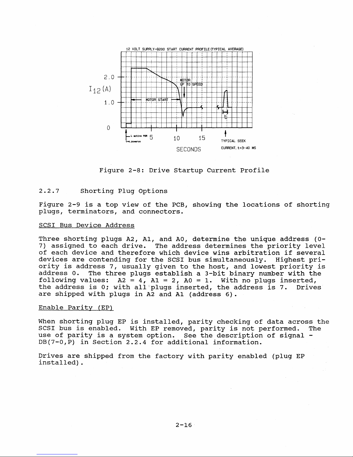
12
VOLT
SUPPLY-Q200
START
CURRENT
PROFILE
(TYPICAL
AVERAGE)
2.2.7
Figure
plugs,
SCSI
Three
7)
of
Bus
shorting
assigned
each
devices
ority
is
address
following
the
address
are
shipped
112
Figure
Shorting
2-9
is
a
terminators,
Device
plugs
to
each
device
are
and
contending
address
o.
The
values:
is
0;
with
2 . 0 ---- -- -- -
(A)
1 . 0
-r-
-
~-:-:
o
~
L
leU.e
t-o,
poweron
2-8:
Plug
top
view
and
Address
A2, A1,
drive.
therefore
for
7,
usually
three
plugs
A2
with
plugs
=
all
in
........
~~~ -~-
: : \ t : I
-
~~~~~
~
i
POR
~
, , ,
-~
aT
R --- --r --------
.~
lP
0 SP
;\
I
~~
--M ------
: j r 7
IV
I
10
--j-----
SECONDS
Drive
startup
options
of
the
PCB,
showing
connectors.
and
AO,
determine
The
address
4,
which
the
given
establish
A1
'plugs
A2
and
=
SCSI
to
2,
inserted,
A1
device
bus
the
a
AO = 1.
(address
~-
--- -- -
EO
I
15
:
..,
--~f
-
-- -----
IL
Jt
•
.j..~
TYPICAL
CURRENT.
Current
the
the
determines
wins
arbitration
simultaneously.
host,
3-bit
and
binary
with
the
address
6).
--
SEEK
t=3-40
MS
Profile
locations
unique
the
lowest
no
plugs
priority
Highest
number
is
of
shorting
address
if
several
priority
with
inserted,
7.
Drives
(0-
level
pri-
is
the
Enable
When
SCSI
use
DB(7-0,P)
Drives
installed)
Parity
shorting
bus
of
parity
are
is
enabled.
in
shipped
.
(EP)
plug
is
a
Section
EP
system
from
is
with
2.2.4
the
installed,
EP
removed,
option.
for
additional
factory
See
2-16
parity
parity
the
with
checking
is
description
information.
parity
enabled
of
not
data
across
performed.
of
signal
(plug
the
The
-
EP
Page 26

P1
RD
55
EP
W5
A2
A1
RD
JUMPERS
(TEST
CONNECTOR)
SMS
5080
(U19)
TERMINA
TORS
J2
J5
J1
~~~_
J3
(MOTOR
CONNECTOR)
BUFFER
RAM
(U16, U17, U18)
MOTOR
Il-r------+--=---
EPROM
(U15)
W1D
8031
MICRO
(U13)
J4
DATA
SYNCRONIZER
PROCESSOR
LED
FYLO
DRIVER
ADC
DIFFERENTIAL
AMPLIFIER (U2)
(U9)
DAC' s
ACTUATOR
(U
(U3,
10)
(U4)
(U1)
U28)
Figure
2-9:
General
Locations
wait
When
STOP
Multiple
ing
received,
with
starts
seconds.
Spin
the
Option
WS
shorting
UNIT command
drives
the
system
a
drive
the
WS
shorting
spinning
Drives
(WS)
from
can
power
is
when
are
plug
the
then
supply.
ready
plug
power
shipped
PCB
be
Layout;
is
installed,
host
started
Once
within
not
installed,
is
applied,
from
via
2-17
Plug,
the
in
the
30
the
Terminator
the
motor
SCSI
bus
sequence
waits
before
to
avoid
and
Connector
for
spinning.
overload-
START/STOP UNIT command
seconds.
the
and
the
factory
motor
in
automatically
drive
this
is
ready
condition.
a START/
is
in
30
Page 27
Self
Seek
option
(SS)
This
drive.
cutes
a
option
SCSI
with
a
bus.
malfunction
Drives
SS
Reset
not
are
installed).
option
Shorting
signal
(plug
If
-RST
not
cold
performs
resets
plete
and
result
takes
all
recalibration,
goes
if
six
commands.
If
warm
is
detected,
a
partial
phase.
useful
when
is
provided
shorting
"butterfly"
No
has
shipped
(RO)
plug
RO
(reset)
installed).
reset
a
is
POR
drive
to
the
a
drive
seconds,
reset
(RO
the
servo
Warm
reset
the
as
a
test
plug
seek
results
SS
pattern.
occurred.
from
the
determines
with
selected,
a
The
cold
Q250
(RO
(Power-On-Reset)
functions
including
reevaluates
SCSI
is
during
plug
drive
bus
free
cold
not
completes
reset
which
installed)
resynchronization,
typically
host
issues
method
installed,
are
given,
factory
whether
reset
and
plug
when
all
phase.
while
time
writing
requires
multiple
to
continuously
the
The
drive
but
with
a
SS
drive
(plug
Q280
never
installed)
the
-RST
write
shorting
Unrecoverable
writing.
the
drive
is
selected
the
and
goes
200
ms.
-RSTs.
drive
need
if
the
disabled
responds
installed)
assert
the
signal
to
disk,
plugs
cannot
current
to
the
It
exercise
continuously
not
drive
(shorting
to
drive
is
performs
except
read
Cold
reset
and
sector,
SCSI
is
particularly
be
connected
stops,
the
or
a
-RST.
immediately
detected:
wait
errors
typically
respond
the
-RST
bus
the
exea
plug
SCSI
warm
a
com-
Spin,
may
to
signal
performs
free
to
bus
reset
it
Both
warm
reset.
plug
not
External
If
an
Leave
Drives
Spare
For
the
with
tion
a
is
and
Drives
installed).
LED
external
W1
installed
are
shipped
Shorting
convenience
spare
affected
cold
are
(W1)
LED
Plug
shorting
by
resets
shipped
will
to
use
with
(P1)
of
customers,
plug
Pl.
meet
from
be
connected
the
W1
installed.
installed
the
the
LED
ANSI
on
drives
2-18
requirements
factory
to
J6,
the
in
position
face
are
set
for
remove
of
shipped
warm
shorting
the
Pl.
for
drive.
from
No
a
"hard"
reset
plug
the
drive
(RO
W1.
factory
func-
Page 28

2.2.8
The
HDA,
of
the"
in
a
pose
inside
Flex
close
thin
16-pin
Flex
Circuit
Circuit
to
the
flexible
connector
preamplifier/write
the
drive.
is
heads
This
a
flexible
circuit
which
to
improve
driver
chip:
printed
is
mates
IC
the
clamped
with
(SSI
circuit
mounted
signal-to-noise
under
J4
501)
on
the
the
is
PCB. A
soldered
cover
in
the
ratio.
and
special
to
sealed
One
terminates
the
circuit
end
pur-
The
2.3
2.3.1
o
Selects
+BUF
through
o
switches
GATE.
o When
falling
multiplied
reversing
media
o
o
Amplifies
Detects
current
transitions
+WR
output
is
PCB
Power-an-Reset
the
HS2,
+BUF
DICEY.
from
writing,
edges
current
the
in
alternate
read
fault
while
UNSAFE.
the
differential
Functional
head
according
HS1,
reading
mUltiplies
of
+BUF
magnetic
signals
conditions
reading,
too
infrequent.
Elements
(PaR)
+BUF HSO,
to
w~iting
WRITE CURRENT. On
WR
DATA,
through
field
directions.
from
such
no
write
signal
and
Warm
to
three-bit
from
the
alternate
and
each
as
current,
If
faults
RDX
and
Reset
logic
the
microprocessor,
when
chip
DICEY
sources
sides
magnetizing
head
about
defective
and
are
RDY.
input
asserts
successive
the
of
the
the
100
times.
heads,
write
detected,
-BUF
coil,
spinning
write
data
asserts
WR
A
cold
paR
the
delay).
voltages
paR
delay
to
thresholds
reset
o Low
o
resets
actuator
is
released
that
initialize
is
SCSI
shorting
the
driver,
paR
dynamically
to
6 V.
ensures
are
triggered
supply
bus
voltage
signal
plug
microprocessor,
and
Transistor
11
ms
to
that
during
set
power
below
by:
-RST
installed
enables
brakes
switches
60
ms
the
power
up.
the
normal
asserted
in
DICEY,
the
the
motor
after
is
To
avoid
power
2-19
by
the
the
drive.
the
5080
electronic
by
perform
+5 V and
stable
multiple
operating
host,
SCSI
return
clamping
each
+12 V are
and
also
with
controller,
all
function.
allows
resets,
ranges
the
spring
coil
normal,
the
and
the
RO
and
(after
output
a
logic
paR
a
a
Page 29

small
hysteresis
Overvoltage
drive
is
between
conditions
recalibrated,
the
are
not
typically
upper
detected.
and
taking
lower
After
six
thresholds
POR
seconds.
is
is
maintained.
released,
the
Circuit
See
(output
ence
11
to
the
CR12
60
Description
schematics
pins
to
ms
reference,
signals.
Pin
56
(-RESET
the
Q250/Q280:
RO
On
5080
plug
the
other
pulls
or
the
installed,
If
the
RO
plug
circuit
by
the
the
At
the
by
-RESET CAP, U29
gates
enables
is
unaffected.
microprocessor,
5080.
start
U24
and
the
13
and
produce
delay.
the
U6
CAP)
the
through
hand,
-RESET
-POR A
is
of
a
U26.
lines
in
SECTION 3
14)
the
When
(output
on
5080
Q28.
when
CAP
is
also
not
installed,
warm
then
Later,
via
DICEY
compare
signals
the
pin
the
5080
is
reset
the
host
pin
pulled
However,
which
reset,
deasserts
the
pin
for
the
the
supply
-PORA, -PORB,
voltage
1)
is
across
comparator
an
by
the
asserts
(now
has
an
low
Q28
a
warm
been
and
remains
flip-flop
the
microprocessor
AUX
6.
POR
voltages
deasserts
input
POR
circuit
-RST
output)
a
cold
reset
triggered
U29
SCSI
lines
circuit.
and
C24
rises
if
a
POR
on
the
low.
reset
turned
now
follows,
by
(Q = pin
-MSD,
clears
Comparators
to
voltage
+POR. C24
above
the
is
either
SCSI
If
the
is
off,
the
three
initiated
through
bus,
RO
triggered.
and
controlled
an
interrupt
9)
is
toggled
-C/D,
the
flip-flop
refer-
sets
the
plug
the
-I/O
U6
the
CR12
POR
at
the
is
POR
from
on
via
and
2.3.2
Refer
motor
three
rents
to
control
Hall-effect
through
replace
coils.
MHz
clock
R97.
Loop
controlled
output.
COIL A
to
generate
mine
that
revolution.
Motor
the
a
commutator
Speed
from
gain
by
C39,
to
COIL B
MOTOR
the
Control
schematic
IC
(U8)
devices
the
three
is
sensed
FYLO.
and
R95,
C40,
R96,
and
voltage
POSITION,
motor
Circuit
in
SECTION 3
senses
mounted
delta-wound
by
indicating
from
Starting
bandwidth
C35,
C4l
is
is
up
to
the
a
Hall
current
of
and
reduce
processed
which
speed.
for
the
differential
around
motor
when
to
signal
is
the
op-amp
C42.
C36
ringing.
by
the
microprocessor
The
2-20
circuit
output
the
motor,
coils.
commutate
and
compared
inversely
current
filters
comparator
signal
is
diagram.
signals
and
drives
The
Hall
current
in
proportional
integrator
the
integrator
U6
(output
checks
two
cycles
The
from
cur-
signals
to
U8
to
are
pin
to
deter-
per
the
the
a 2
to
2)
Page 30

Q24
turns
processor
EMF
generated
whose
outputs
off
causes
the
by
are
motor
DICEY
the
spinning
clamped
when
to
-POR B is
deassert
motor
to
6
V,
asserted
-SPIN,
flows
producing
which
through
dynamic
or
when
turns
the
the
off
IC
drivers,
braking.
micro-
Q8.
Back
2.3.3
When
the
thus
At
delay
the
back
forcing
power-on-reset,
allows
discharges
and
Q14
motor
If
the
Only
zone;
drive
to
the
+12
+12
milliseconds
AIRLOCK
during
2.3.4
A
5080
CMOS
SCSI
technology
conform
meet
The
it
low
the
5080
is
and
strapped
selected
Electronic
drive
EMF
C36
turn
the
V
V
dc
5080
Controller
to
standard
ANSI
can
the
IOEN
when
is
powered
from
the
the
the
headstack
driver
and
on.
Twice
actuator,
dc
supply
is
maintained,
are
operates
this
period.
SCSI
reduces
standards,
operate
to
operate
pin
address
Return
slowing
-POR
clamps
then
has
required
about
Bus
IC
5 V
with
high.
bits
Spring
down,
motor,
into
turns
Q3
currents
the
U8
per
revolution
through
failed,
more
30
Controller
is
used
the
power
logic
and
levels.
are
various
with
Pins
MAD7-5
the
electronic
switching
the
landing
off
after
to
fall
current
Q7
Q14
the
circuit
current
to
move
the
seconds
to
implement
consumption.
The
connected
microprocessors;
an
8031
XOR
are
or
A7-A5
110
zone.
a
delay
to
a
integrator
passes
and
R42
is
supplied
actuator
later.
SCSI
directly
8032
are
(address
return
it
to
safe
current
to
still
Do
the
All
bus
by
tying
strapped
spring
the
set
by
level
output).
ground.
functions,
to
into
not
handle
SCSI
inputs
pins
to
the
in
this
range
utilizes
actuator,
C29.
(while
Q4,
from
the
the
the
actuator.
landing
the
interface.
and
of
the
SCSI
application
the
CONFIG
so
the
CO -DF).
This
Q5
Q7,
but
outputs
5080
bus.
pin
5080
if
is
On
command
the
drive
nected
Figure
emphasizes
shown
on
Registers
over
(1)
the
switch
deassert
nals
from
SELECTION/
logic
for
of
and
to
5080
2-10
is
the
the
schematics
in
the
MAD
bus.
the
SCSI
the
RESELECTION
arbitration.
the
microprocessor,
the
options
pins
a
IN
conceptual
external
5080
In
5080
bus
host,
from
signals,
and
are
this
and
set
0-5.
block
interfaces.
in
SECTION 3
written
way,
target
(3)
(4)
set
ARBITRATION
by
read
the
the
shorting
diagram
The
and
and
for
example,
to
initiator
the
the
programmable
2-21
5080
signals
in
read
state
phases.
reads
of
Figure
by
the
plugs,
the
5080.
mentioned
2-4.
the
microprocessor
the
microprocessor
mode,
of
SCSI
timing
The
SCSI
which
(2)
5080
Figure
assert
bus
for
address
are
below
and
control
the
provides
of
con-
2-11
are
can
sig-
SCSI
Page 31

,--------------------------------------------1
I I
I I
I I
SCSI
\
REGISTERS/
CONTROL
LOGIC
V
t\
~
NTERFACE
1
r
\
-y
DMA
NTERFACE
STROBE
HOST
STROBE
DATA
(REG
6,7)
Figure
STROBE
ON
TROLLER
1.0
(REG
I
I
I I
L ____
2-10:
DMA
TO
HOST
REGISTER
5)
~~
MICROPROCESSOR
INTERFACE
5080
HOST
TO
DMA
REGISTER
STROBE
SELECT
----
Conceptual
READ
REGISTER
MUL
TIPLEXER
REG.O
REG. 1 REG.
~J
INPUT
PORT
~----~~-YI
2
I
I
____ J
Block
...-_--==:::;--- OPTIONS
Diagram
BUFFERED
llATA
DMA
TO/FROM
MADO-7
ADORESS/
DATA
roRD,
BUS
CmHROL
BUS
INTERRUPT
IOWR,
PLUGS)
~
1.S
I
~*=-r-
TTL
INPUT
(SHORTING
DICE {
ALE
Figure
SELECT
2-11:
WRITE
MULT
5080
2-22
HOST
IPLEXER
Interface
HOST
INTERFACE
SCSI
BUS
Diagram
Page 32
The
microprocessor
edge
of
strobes
ALE
data
(address
from
strobes
latch
the
MAD
an
address
enable).
bus;
-IOWR
into
If
the
strobes
the
5080
5080
data
on
is
selected,
to
the
the
falling
MAD
-lORD
bus.
DICEY
controls
(buffered
o When
o When
Handshaking
DICEY)
buffer
and
RAM
arbitration
2.3.5
Before
2.2.2.
diagram
details
reading
Follow
of
of
Seeking
data)
5080.
to
HOST
RAM.
the
between
-DMA
without
logic
Servo
the
the
a
DMA
bus:
-DMA
-DMA
register.
-DMA
-DMAIENB
HOST
to
ACK
is
Control,
this
this
drive.
servo
read
I/O
I/O
is
CLK
is
or
asserted,
strobes
deasserted,
turns
DMA
register
DICEY
(from
and
DICEY).
intervention
set
by
AMC
section,
explanation
Figure
signals
write
the
the
and
read
2-3
in
on
by
12
on
the
to
the
the
onto
5080
DICEY
the
MHz
Servo
the
Figure
shows
wedges.
buffer
data
data
data
5080
the
is
handles
5080.
clock
AGC
summary
the
RAM
flow
from
is
the
flow
drivers,
bus.
controlled
Timing
from
description
2-4,
a
disk
over
is
from
bus
from
the
RAM
to
placing
by
-DMA
addressing
for
FYLO.
simplified
format
BDATAO-7
to
the
the
the
5080
data
REQ
of
the
5080
in
section
block
including
DMA
to
from
(to
the
While
a
numbers
position.
sures
how
the
nearly
processor
the
highest
responding
data
If
infers
the
Track
While
wedge
is
data
the
bursts
Following
track
are
servo-burst
when
the
written
drive
from
As
peak
the
attempts
amplitude,
to
invalid,
from
head
in
following,
stored
amplitudes
head
on
each
is
seeking,
the
data
each
amplitudes
bursts
that
data
all
bursts
position
the
next
in
is
centered,
side
in
wedge
are
to
use
because
burst.
from
wedge.
RAM
of
the
passes
in
from
the
as
in
the
the
read
servo
of
the
centered
the
servo
the
But
if
the
next
a
wedge
previous
track,
they
order
the
head
data
circuit
bursts,
under
burst's
under
track
head
the
largest
is
head
are
read.
to
center
equally
track--the
reads
thus
the
moving
preambles,
the
number
is
over
checksum
amplitude
invalid,
data,
and
sector
Also,
the
overlaps
microprocessor
the
determining
head,
moving
from
the
bits
the
and
then
the
head
servo
which
head.
the
servo
the
track
AMC
depend
The
burst
track
indicate
burst
microprocessor
reads
numbers
AMC
over
the
from
measures
the
servo
positions
the
meamicro-
that
is
used.
data
each
track:
bursts
head
upon
with
cor-
the
from
the
2-23
Page 33

the
head
difference
the
head
fifth
of
so
the
between
is
centered;
a
head
AMC
gives
the
width),
burst
if
the
equal
the
drive
amplitudes
amplitudes
difference
stops
for
is
a
measure
becomes
reading
these
too
or
two
of
how
large
writing.
bursts.
closely
(about
The
one-
Adaptive
To
improve
sured
these
Up
values
Sequence,
o
o
Gain
during
KAG,
physical
upon
temperature,
at
forward
compensate
heads.
NULL
required
windage,
and
NULL I is
until
measured
the
two
cylinders.
constantly
Parameters
servo
operation,
recalibration
are
updated
Figure
or
other
the
middle
I,
to
compensate
the
same
values
2-15.
servo
head
factors.
value,
for
or
force
to
the
measured
head
at
for
accurately
measured
three
and
while
gain.
width,
KAG
is
track,
used
burst
bias.
overcome
flex
circuit,
for
accurately
the
inner
all
heads.
Since
NULL I changes
adaptive
stored
the
This
though
Since
measured
during
by
the
amplitude
This
forces
any
by
changing
cylinder
predicts
and
the
gain
in
RAM.
drive
is
is
essentially
it
depends
the
head
for
each
recalibration.
microprocessor
variations
is
the
on
the
gravity
offset
in
the
centers
and
Linear
extrapolation
the
with
value
parameters
In
addition,
operating.
to
width
head,
dc
actuator
actuator
(in
some
the
actuator
value
over
the
outer
parameter
temperature,
in
RAM
See
a
measure
a
lesser
doesn't
but
This
to
predict
when
from
orientations),
in
small
track.
cylinder,
between
for
is
updated.
are
meatwo
the
of
extent
vary
only
is
once--
a
and
switching
current
bearings,
circuitry.
steps
It
and
all
it
of
Power-
the
with
feed-
is
is
the
is
AMC
Circuit
The
AMC
signal,
o
measures
integrating
Servo
data
from
inner
predicts
changes
value
stored
AGC
overrides
gain
of
Description
AGC,
the
bursts.
and
outer
the
with
is
constantly
in
RAM.
the
U2
servo-burst
it,
gain
of
It
cylinders.
parameter
temperature,
measured,
When
the
(A)
reading
CAGC
AGC
amplitude
and
then
a
head
is
measured
Linear
at
other
a
fixed
signal
amplifier.
converting
2-24
when
cylinders.
and
servo
from
by
full-wave
reading
for
each
extrapolation
offset
the
data
U2
it
from
updated
in
(B),
from
head
position
head,
To
correct
the
offset
a
wedge,
and
controls
rectifying
analog
at
the
accurately
for
predicted
is
Servo
the
to
digital.
the
Page 34
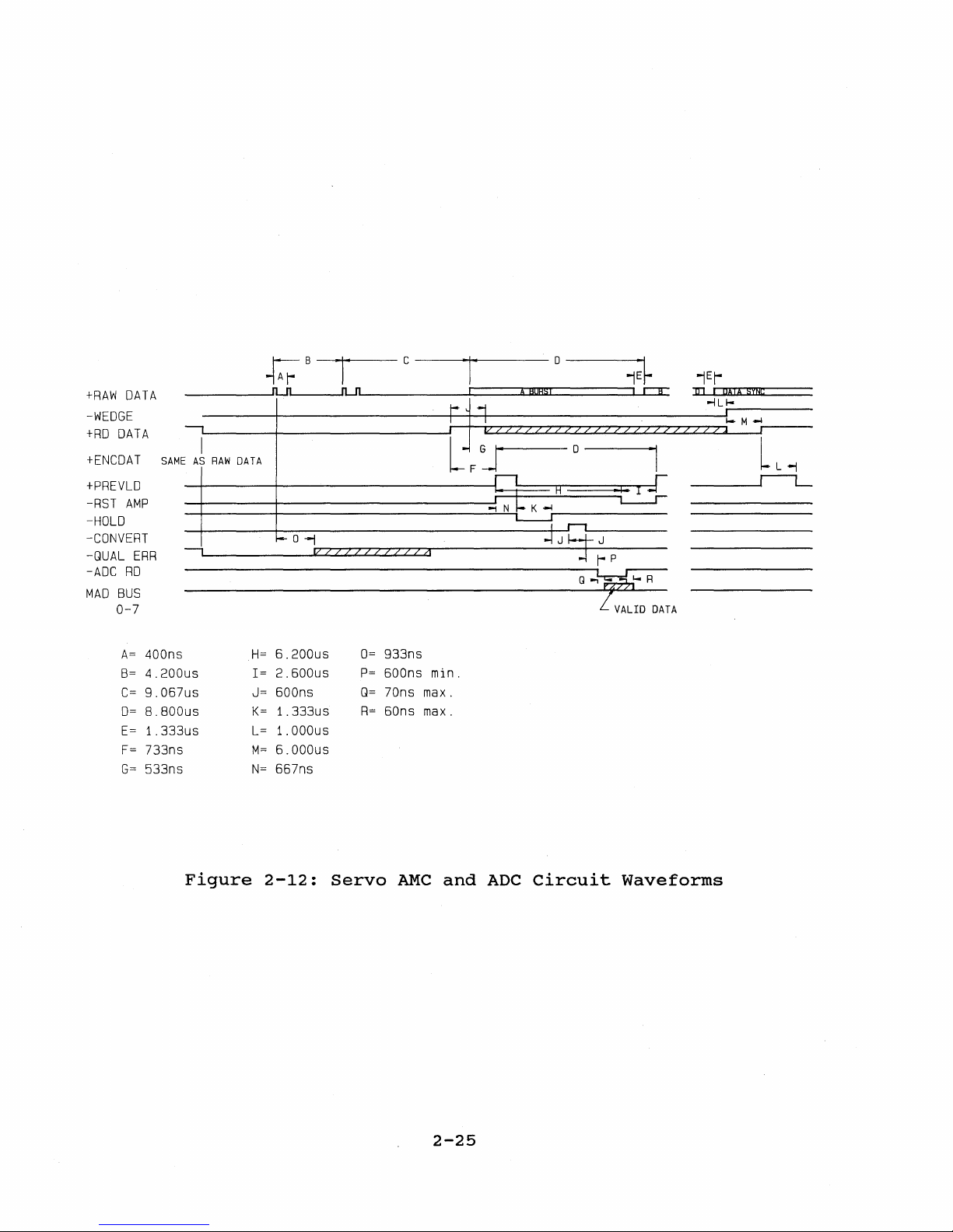
+RAW
DATA
-WEDGE
+RD
DATA
+ENCDAT
+PREVLD
-RST
AMP
-HOLD
-CONVERT
-QUAL
MAD
-ADC
RD
BUS
0-7
A=
B=
C=
0=
E=
F=
G=
ERR
400ns
4.200us
9.067us
B.BOOus
1.
733ns
533ns
SAME
-,~
333us
AS
I
RAW
____________
DATA
H=
1=
J=
K=
L=
M=
N=
~
n...J1
f-O-j
6.200us
2.600us
600ns
i.333us
i.OOOus
6.000us
667ns
B
-"II---'
~v./~/~/~/~/~/~/./~/~/~o
n...J1
- C
0=
933ns
P=
600ns
Q=
70ns max.
R=
60ns
--t---I'
min.
max.
i A
1-,
-j
I I
- 0
-----l1~~
BuRS!
0
i
r=r
l:F~J
H
~NJ-K-I
I
~J
l~
J
m i
IIA!!
sYNC
--lU"
J-M-I
I
~
LL-j
Figure
2-12:
Servo
AMC
and
2-25
ADC
Circuit
Waveforms
Page 35
Refer
Figures
amplifier
3)
to
sistor
present.
At
transistor
C72,
During
ing
C72.
the
ing
to
in
transistor
a
proportional
the
initializing
current
The
preamble
the
the
schematic
2-12,
is
+READ
(6,
7,
beginning
(12,
the
preamble
from
charge
signal,
current
5-1,
8)
5-2
SIG
array
current,
in
of
13,
the
the
accumulates
that
diagrams
and
and
U11
U11
a
burst,
14).
sample
period
current
until
would
5-3.
-READ
full-wave
which
sinks
In
of
FYLO
otherwise
in
the
-RST
turn,
and
a
burst,
mirror
during
asserts
SECTION
The
differential
SIG.
rectify
is
mirrored
mirrored
AMP
this
hold
to
an
flow
3,
Transistors
current
is
asserted,
biases
integrator
FYLO
flow
integral
deasserts
through
+HOLD
through
and
the
by
and
the
signal
signal
Q17
Q20
U12
number
turns
CR5.
waveforms
(1,
2,
and
when
which
on
and
(pins
-RST
CR5
of
from
3,
and
convert
Q18.
no
burst
turns
discharges
5,
AMP,
and
charge
cycles
on
Q19,
the
and
Tran-
6,
in
5,
is
off
7).
allow-
of
sink-
AGC
4,
it
U11
BURST
portional
FYLO
number.
to
Burst
Maximum
Zero
Servo
Follow
To
placing
strobes
DAC.
to
input
on
converts
and
Therefore,
bursts,
data
PEAK,
asserts
assert
Amplitude
AGC
control
The
255
to
when
overrides
from
the
to
the
-CONVERT,
The
microprocessor
-ADC RD.
Circuit
this
(decimal)
explanation
the
8
bits
the
bits
U12
Q10,
-WEDGE
it
to
the
but
the
the
output
charge
U12
2.5
3.7
Description
Servo
corresponding
(pins
an
is
a
the
Servo
U2
user
AGC,
into
DAC
emitter
high-current
the
1,
input.
asserted,
CAGC
AGC
(B)
areas.
of
U12
on
C72,
the
AMC
places
Integrator
volts
on
the
the
DAC
2,
3)
follower.
and
signal
sets
circuit
(pin
microprocessor
to
with
op-amp
The
output.
produced
the
7),
and
thus
DAC
converts
it
on
Output
schematics
the
desired
-DAC
output
DAC
output
Transistor
then
sets
U2
mirrors
(A)
the
is
now a
to
the
this
the
in
Servo
CS
and
is
This
by
output
pulse
amplifier
amplifier
voltage
burst
voltage
MAD
bus
U10
ADC
o
(decimal)
255
SECTION
selects
-WR,
3.7
is
divided
array
the
current
detector
amplitude.
by
Output
3.
AGC
AGC
on
and
to
7.4
U27
connects
gain
gain
inversely
to
causing
DAC
the
asserts
volts
and
becomes
is
from
U2
when
when
an
8-bit
DICEY
U28
MAD
switched
to
(B).
reading
by
bus,
+AGC
for
Q10
CAGC,
reading
proWhen
°
the
and
2-26
Page 36

2.3.6
Actuator
Positioning
Circuit
While
control
tor
current,
bus,
strobes
asserts
for
0
U5
is
ence
voltage--the
rents
DAC
output
current.
settling
turns
U4
(A)
Driver
through
actuator
put
of
voltage
giving
The
R-C
actuator
ground
inductive
reading
the
+ACT
to
255
another
is
obtained
While
and
on
Q11
is
an
stage
Q15
coil
the
across
accurate
network
coil
plus
transients
the
actuator,
places
the
DAC.
(decimal)
voltage
of
128
following.
and
error
U4
limit
a
error
R42
time
C62
following,
the
8
bits
bits
The
into
output
DAC
amplifier;
full
even
range
though
(decimal)
seeking,
connects
amplifier,
(B)
has
the
dissipation
differential
amplifier.
and
R43,
positioning.
from
output
constant;
and
C63
across
refer
microprocessor
corresponding
actuator
of
input.
of
positive
a
negative
corresponds
the
gain
The
gain
R72
a
into
a
part
differential
current
U5
senses
amplifies
to
input
the
compensate
the
actuator
to
DAC
op-amp
its
output
of
U5
is
switched
the
of
in
U4
that
of
R-C
network
U4
the
schematics
calculates
to
U3
U21
and
supply
to
is
feedback
the
output.
(B),
is
the
it
by
U4
(B).
coil.
the
current
with
-DAC
is
3.7
swings
volts
around
negative
is
not
zero
four
(nominal)
times
by
+GAIN
path.
actuator
Power
and
force
proportional
current
four,
(A)
from
as
and
compensates
U4
CR13 - CR16
in
SECTION
the
desired
on
CS
and
actuator
available.
its
LOW,
driver
transistors
through
the
closes
(A)
suppress
the
-WR,
to
7.4
the
refer-
actuator
gain
which
chip
to
the
difference
the
for
output
3.
actua-
MAD
and
volts
cur-
when
U4.
the
out-
loop,
the
to
To
A
Q12
2.3.7
Follow
drive,
Figure
The
alternating
voltage
This
RDX
8464
voltage
and
pulse
balanced
errors.
R57
and
output
Read/Write
this
and
circuit
the
2-13.
across
is
RDY) , and
detector
five
Q1,
R63.
to
Q9, Q2,
the
pole
Q23
U2
Circuit
description
schematics
magnetic
the
coil
preamplified
ac
coupled
U2.
filter
and
and
Q26
(B)
pulse
in
fields
in
The
that
Q16
are
on
SECTION
on
the
head
by
the
to
the
AGC
slims
drive
emitter
detector
Figure
3.
the
disk
selected
chip
AGC
amplifier
the
the
followers
inputs.
2-27
2-4,
The
generate
in
the
amplifier,
output
pulse
filter,
a
block
waveforms
by
+BUF
flex
U2
is
to
reduce
which
that
diagram
are
a
differential
HSO
- +BUF
circuit
(A),
filtered
shouldering
is
terminated
couple
shown
(giving
part
by
the
of
HS2.
of
filter
the
in
the
a
in
Page 37

The
AGC
the
U2
constant
R9
set
high
peak
amplitude
circuit
(A)
(actually,
the
signal
is
+ENC
samples
amplifier
averaging
amplitudes
low.
DA
T A
---+.---J
+RD
ClK
gain
four
time
the
to
times
constant
filtered
keep
the
and
increases
differential
the
average
voltage
so
the
applied
gain
more
signal,
peak-to-
to
decreases
slowly
and
peak
VREF).
rapidly
when
controls
amplitude
C9
the
signal
and
for
Each
disk.
the
time,
zero
tive
that
signal
The
peaks
easily
crossings:
and
negative
exceed
one-shot,
signal,
+RAW
ferentiation
When
output
PLL
GATE
user
over
in
DATA,
DICEY
As
no
data
(+RD
synchronization
twice
data
a
valid
a
high
which
de-asserts
the
preamble
positive-going
with
+READ
peak
8464
to
first
zero
detected.
to
the
level
producing
DATA.
time
is
being
CLK)
per
sector:
preamble.
preamble,
gain
is
tracking
buffered
is
transitions
CLK
to
Figure
2-13:
corresponds
differentiates
crossings
Noise
qualify,
peaks
of
set
a
pulse
C7
sets
constant.
read,
locked
to
time.
once
FYLO
and
mode
+RAW
+PLL
HBW
being
read,
determine
to
with
pulses
they
the
by
VHYS.
for
the
AND
the
FYLO
at
asserts
DICEY
and
DATA.
for
of
+ENCODED
which
Read
a
magnetic
a
must
filtered,
each
pulse
gate
15
MHz
predicts
the
+PREVLD
then
allow
lower
+READ
bit
Circuit
the
high
rate
are
be
Qualified
signal
width,
U23
clock
A
burst
asserts
fast
Later,
PLL
gain
CLK
DATA.
cells
Waveforms
transition
filtered
of
change
suppressed
caused
but
by
undifferentiated
zero
peak.
and
(pin
12)
input,
a
preamble
preamble,
whenever
+PLL
phase
while
and
quickly
DICEY
contain
written
signal
to
of
by
qualifying
alternating
crossings
This
R1,
keeps
thus
the
HBW
lock
track
less
Cl
and
and
head
to
onto
following,
jitter.
is
set
the
reducing
asserts
again
synchronizes
strobes
encoded
on
convert
voltage
posi-
signal
trigger
the
output
the
U1 PLL
at
should
hold
the
+ENCODED
to
+RD
data
the
with
the
a
dif-
the
+READ
the
be
PLL
the
DATA
2-28
Page 38

pulses,
to
an
a
DMA
and
a-bit
transfer.
then
data
transforms
byte.
The
this
byte
data
is
from
passed
2/3
from
RLL
DICEY
(1,7)
to
encoded
buffer
data
RAM
in
R17,
VCO
set
pump
RIB,
frequency,
the
current.
selected
write
See
SCSI
of
the
write
Controller
encodes
(1,7)
DICEY
the
six
the
write
coded
asserts
flex
non-inverting
inputs
current
CURRENT
output
on
Q21,
CURRENT.
near
zero.
C20,
PLL
loop
for
the
description
circuit
the
data
data.
circuit
are
to
ground.
of
the
inserting
On a
and
C21
and
R21
bandwidth
R19,
10
Mbit/sec
C15,
of
operation.
is
stored
from
-WR
GATE
chip
buffers,
1A - 6A;
in
the
The
outer
tracks:
R22
reset,
set
the
the
VCO
and
and
C16
data
the
Flex
in
RAM
its
B-bit
when
from
it
preamplifier
used
the
corresponding
head
is
proportional
microprocessor
through
in
parallel
POR B turns
PLL
operating
damping,
compensate
Circuit,
In
write
and
form
detects
to
gain
rate.
mode,
passed
to
improve
DICEY,
with
off
Q22,
and
bandwidth.
current.
and
integrate
for
section
data
to
DICEY
a
serial
a
user
to
area,
write
signal
outputs
to
the
compensates
it
asserts
R23
and
thus
reducing
C17,
phase
2.2.B,
received
stream
thereby
driver.
immunity
are
current
for
increasing
WRITE
the
shift,
via
1Y
the
AUX
C22
sets
C1B,
PLL
for
an
by
DMA.
of
2/3
switching
U20
to
- 6Y.
from
lower
5,
CURRENT
the
and
R20
charge
and
are
outline
the
50BO
DICEY
RLL
contains
noise:
WRITE
turning
WRITE
to
2.3.B
FYLO
of
timing
the
is
a
pinout.
o
o
o
o
o
FYLO
custom
Timing
IC
functions.
FYLO
Accepts
+ENCODED
Derives
the
2 MHz, 12MHz,
Outputs
Controls
-RST
Begins
AMP
servo-burst
Controller
proprietary
See
performs
+RAW
DATA,
DATA.
the
2
MHz
-WEDGE
the
servo
and
+HOLD.
device
the
clock
and
to
identify
IC,
to
U9
following
and
buffers
15
AMC
sample
AID
conversion
2-29
and
Quantum
on
the
from
MHz
the
clocks.
the
Xtal
Oscillators
that
schematics
functions:
the
signal
12
MHz
wedge
and
hold
by
incorporates
in
to
clock,
area.
timing
asserting
a
SECTION 3
produce
and
with
-CONVERT.
number
for
buffers
outputs
Page 39
o
Asserts
through
+READ
the
read
GATE
data
to
indicate
synchronizer.
when
data
should
be
processed
o
o
Several
factured;
the
microprocessor,
a
metal
oscillator
(pins
3 -
2.3.9
DICEY
is
Quantum
U14
on
the
the
block
DICEY
performs
laneous
chips
on
Asserts
should
Asserts
DICEY
criteria,
the
correct
three
Note:
inhibited
writing
variations
the
PCB
can
at
module
6)
in
DICEY
a
custom
and
designed
schematics
diagram.
"glue
the
logic,"
PCB,
+PREVLD
be
present.
+QUAL
that
which
dc
erase
to
avoid
in
data
of
accomodates
with
U25,
or
with
U23
is
Data
data
All
several
and
to
ERR
the
wedge
are:
times,
fields.
overwriting
a
wedge.
in
the
the
crystal
a
15
(2)
a
driver
required
Controller
controller
by
Quantum
in
SECTION 3
pins
functions,
thereby
improving
indicate
to
indicate
area
(1)
and
(2)
Moreover,
sector
oscillator
either
MHz
crystal
dual-
ICs
in
only
IC
IC,
for
conform
listed
significantly
the
to
DICEY
to
does
not
sector
no
pulses
the
servo
if
QUAL
(1)
a
frequency
a
metal
for
option
a
100-pin
the
Q200
for
the
to
standard
below,
drive
that
the
microprocessor
meet
and
echo
are
tracks,
the
microprocessor
ERR
circuits
12
MHz
and
associated
12
MHz
can
(1).
device
series
pinout
including
reducing
reliability.
a
the
pulses
detected
is
asserted.
crystal
and
at
U25.
disk
and
5 V
valid
preamble
qualification
appear
in
writing
have
been
driven
driver
15
MHz
AND
proprietary
drives.
Figure
logic
levels.
miscel-
the
number
and
the
is
inhibits
manu-
IC
crystal
gate
2-14
of
at
by
in
to
See
for
DICEY
has
o
o
o
o
these
features:
Controlled
over
the
MAD
Microprocessor
it
can
write
status,
Performs
etc.
serial-to-parallel
conversions.
Encodes
from
means
the
that
all
disk,
by
microprocessor,
bus.
sees
to
control
data
written
using
the
code
DICEY
data
a
2/3
maps
2-30
as
to
two
which
a
transfer,
and
disk
RLL
data
communicates
set
of
34
registers
or
parallel-to-serial
and
decodes
(1,7)
bits
code.
into
read
The
three
to
all
with
to
determine
data
notation
code
DICEY
which
read
bits,
Page 40
PlL
AD
1IA
AD
PRE
HI
811
DATA
DATA
CLOCK
VLD
..
DICEY
SERIAL
CHANNEL
RESISTER
I I
11
III
11
IC
BUS
..
-
•
,
BlFFEA
-
DATA
o
o
IF
ADDAIDATA
UTCI£D
ADDA.DUT
and
that
o
bits
Generates
after
and
pll
Os).
Detects
there
is
-
..
AUX
I/O
BUS
Figure
the
between
a
sync
locks
sync
a
drop
--
UP
INTERFACE
-"""
2-14:
encoded
each
time-out
on
pattern
out,
CONTROL
DICEY
bit
1
bit.
the
(100100)
drop
.....
,
MASTER
UNIT
Block
stream
error
preamble
in,
DMA
CONTROLLER
Diagram
has
if
(an
and
generates
or
shifted
BlFFER
AIlIlA.
-
BlFFER
CONTROLS
SCSI
INTEIFACE
between
sync
is
alternating
bit.
one
not
a
and
detected
field
sync
seven
of
error
Is
if
o
o
o
o
Controls
priority:
data,
DMA
cycles
Control
Disk
in
Can
and
and
the
read
the
access
(1)
(2)
microprocessor,
are
Unit,
write
serial
and
write
SCSI
bus)
sec.
to
buffer
disk,
including
controlled
synchronized
functions
channel,
to
buffer
at
the
RAM
via
user
and
by
are
(3)
a
state
to
the
controlled
synchronized
RAM
burst
transfer
2-31
DMA
data
5080
15
(to
transfers,
and
SCSI
machine
MHz
by a state
to
READ
and
rate
servo
controller.
clock
CLOCK.
from
of
in
both
in
position
the
from
1.25
this
Master
FYLO.
machine
the
disk
Mbytesj
Page 41
o
Checks
buffer
RAM
during
initialization.
o
o
o
o
o
2.3.10
Q250
and
processors
DisCache
No
Yes
Generates
Refreshes
contains
LAD
0-7).
Provides
contains
4.2.1)
latches
additional
12-byte
.
Microprocessor
Q280
as
drives
shown
Table
Microprocessor
8031
8032
parity
Buffer
use
in
the
2-3:
and
checks
RAM.
for
the
low-byte
microprocessor
ECC
syndrome
and
EPROM
12
MHz
industry-standard
following
Microprocessors
Internal
Data
128
256
RAM
8
X
X 8
parity,
generator.
table:
FIFO
Buffer
16
64
EPROM
and
Kbytes
Kbytes
for
I/O
Buffer
RAM
buffer
address
(pins
(See
8-bit
RAM
RAM.
(outputs
AUX
section
micro-
Buffer
KBytes
14
KBytes
60
0-7).
The
Internal
access.
Firmware
U15.
and
There
without
2.4
This
which
After
the
section
is
RAM
SCSI
seconds.
data
RAM
Communication
for
the
drive
are
four
DisCache.
Power-Up
Sequence/Recalibration
explains
shown
tests
bus,
in
Figure
and
although
is
with
is
different
the
circuit
the
used
for
other
stored
EPROMS:
special
2-15.
initialization,
drive
look-up
devices
in
a
features
cannot
32
for
tables
is
KB
read
over
EPROM,
Q250
of
the
the
or
that
the
a
and
Q280,
power-up
drive
write
require
8-bit
27256,
can
for
fast
MAD
located
each
with
sequence,
respond
several
bus.
at
to
2-32
Page 42

No
mechanical
Q280,
the
servo
toward
while
as
the
the
the
actuator
wedges.
middle
radial
or
absolute
finds
At
power-up,
of
the
velocity
position
its
disk,
is
zero.
information
position
the
then
by
position
braking
is
reading
is
determined
and
reading
used
in
information
the
the
by
wedges
Q250j
from
seeking
Once
the
actuator
position,
information,
into
then
the
even
buffer
read
list
if
one
cylinder
2.5
This
section
Sequence,
Series
The
Programmers
READ
transfer
checks
sector
action
MODE
the
is
taken
SELECT
2.6
actuator
seeks
the
peak
the
RAM.
from
is
stored
or
0,
and
Read
explains
Figure
command
length
defect
read
is
command.
write
position
to
the
amplitudes
adaptive
The
reserved
on
more
is
copies
ready.
Command
2-16.
Manual.
contains
in
blocks.
list
into
buffer,
that
Command
outer,
gain
W-list,
tracks
each
Sequence
the
special
For
the
and
specified
Sequence
is
known,
middle,
of
parameters
or
into
surface
is
damaged.
additional
starting
Before
seeks
the
data
by
the
and
the
servo
working
buffer
so
that
features
reading
to
the
is
the
Error
drive
inner
is
tracks,
bursts
are
calculated
list
of
RAM.
it
is
Finally,
of
the
information,
logical
block
each
correct
checked
Recovery
recalibrated:
are
read.
defective
A
duplicate
always
the
drive
Read
see
address
sector,
position.
for
correctness;
Parameters
and
at
From
and
written
sectors,
copy
available,
seeks
Command
the
Q200
and
the
Q250jQ280
After
the
each
of
this
is
of
to
the
each
the
the
This
section
Sequence,
Series
The
Programmers
WRITE
transfer
checks
the
Writing
the
buffer.
transfers
(actually
length
and
Q250jQ280
of
from
explains
Figure
command
length
defect
to
disk
Then,
data
interleaved,
data
the
buffer
sends
2-17.
contains
in
list
doesn't
from
has
Status
the
For
Manual.
blocks.
and
start
the
Q250jQ280
the
SCSI
a
been
to
the
transferred
and
special
additional
the
Before
seeks
byte
disk,
Message
starting
until
bus
at
features
writing
to
the
a
writes
to
buffer
a
time).
from
the
transfer
to
2-33
of
information,
logical
each
correct
complete
to
the
almost
When
the
SCSI
the
host.
the
write
see
block
sector,
position.
block
disk
from
simultaneously
the
full
bus
is
complete
Command
the
address
the
is
available
buffer,
transfer
to
the
Q200
and
Q250jQ280
buffer,
and
the
the
in
and
Page 43

FIND
SEEK
READ
SEEK
MEASURE
ACUATOR
AND
SERVO
TO
CYLINDER
HEAD
SERVO
POSITION;
PIVOT;
BURST
O.
BURST
822
SEEK
TO
HEAD
MEASURE
AMPL
ITUOES.
SEEK
TO
MID
HEAD
MEASURE
AMPLITUDES.
CALCULATE
PARAMETERS
NULL
READ
DEFECT
SECTORS
PROTECTED
CYLINDER
0
SERVO
ALL
CYLINDER.
O.
SERVO
ALL
ADAPTIVE
KA.
I.
AGC
LIST
0-11
BUFFER
BURST
HEADS
BURST
HEADS
FROM
INTO
RAM
O.
Figure
2-15:
Power-Up
2-34
Sequence
Page 44

HOST
ARBITRATES
FOR
SELECTS
BUS,
DRIVE
SET
NEXT
READ
SECTOR
INTO
DICEY
COMMAND
SENT
SCSI
READ
COMMAND
PULLED
B031
DECODE
READ
COMMAND
CHECK
DEFECT
LIST
VIA
BUS
INTO
RAM
SERVO
INTERRUPT
READ A SECTOR
FROM
DISK
TO
BUFFER
DICEY
Y
START
SEEK
CHECK
DEFECT
LIST
WAIT
FOR
SEEK
COMPLETE
TRANSFER
FROM
BUFFER
TO
SCSI
SEND
STATUS
TO
HOST
BEGINS
CHECK
ERROR
PAGE
FOR
OPTIONS
ACT
PER
OPTIONS
*RETRY
*CORRECT
*NO
CORRECTI
*ETC
W/ECC
ON
FINO
SECTOR-1
Figure
2-16:
Read
2-35
SEND
MESSAGE
TO
HOST
Command
Sequence
Page 45

A
FINO
SECToR-l
Figure
2-17:
write
2-36
Command
Sequence
Page 46

SECTION
3.
Q200
SERIES
ENGINEERING
DRAWINGS
The
following
Boards
for
applicable,
Figure
Figure
Figure
Figure
Figure
Figure
Figure
Figure
Figure
Figure
Figure
Figure
3-1:
3-2:
3-3:
3-4:
3-5:
3-6:
3-7:
3-8:
3-9:
3-10:
3-11:
3-12:
drawings
several
please
Printed
Schematic,
Schematic,
Schematic,
Printed
Schematic,
Schematic,
Schematic,
Printed
Schematic,
Schematic,
Schematic,
illustrate
revisions.
refer
to
PCB-7
Circuit
PCB-7,
PCB-7,
PCB-7,
PCB-8
Circuit
PCB-a,
PCB-a,
PCB-a,
PCB-9
Circuit
PCB-9,
PCB-9,
PCB-9,
the
Depending
PCB-7,
PCB-a,
Engineering
Board
Sheet
Sheet
Sheet
Parts
1
2
3
Engineering
Board
Sheet
Sheet
Sheet
Parts
1
2
3
Engineering
Board
Parts
Sheet
Sheet
Sheet
Q200
Drawings
Drawings
Locations
Drawings
1
2
3
Series
on
the
or
PCB-9
Locations
Locations
Printed
specific
drawing
(PCB-7)
(PCB-a)
(PCB-9)
Circuit
PCB
groups.
that
is
3-1
Page 47

-
C&7
- C68
CJ
-
WiD
C54
1
QUANTUM
CORP.
Q200
PCB
7
FAB
10-22007
SILKSCREEN
ARTWORK
30-22007
REV
02
CRD
A026
4-4-86
KRL
or
5
~
::J
Ii
-
CSO
CSi
R5&
lit
R5&
-
,.,
-
III
~
..
II
-
i!
..
"
~
1I
f'\'
~
-
U
-
Ril
Figure
3-1:
Printed
Circuit
Board
Parts
Locations
Page 48
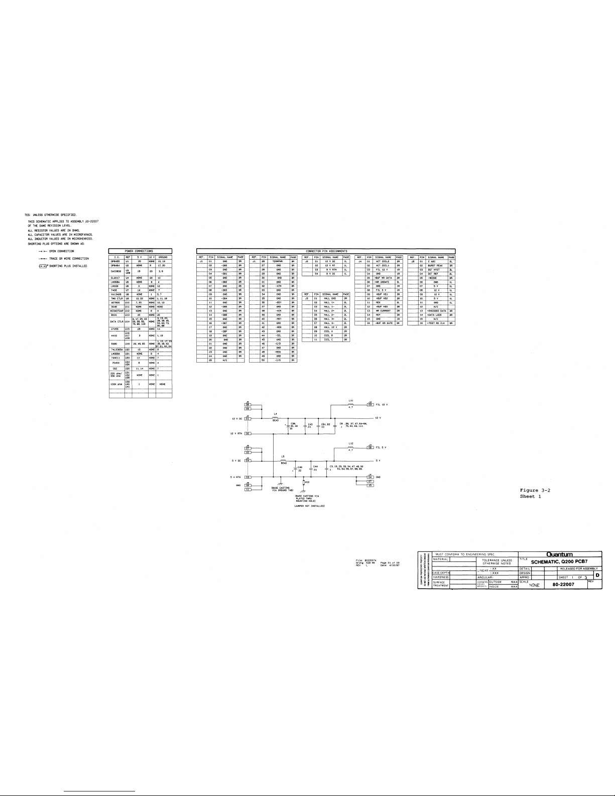
TES:
UNLESS
OTHERWISE
SPECIFIED.
THIS
SCHEMATIC
APPLIES
TO
ASSEMBLY
20-22007
OF
THE
SAME
REVISION
LEVEl.
ALL
RESISTOR
VALUES
ARE
IN
OHMS,
ALL
CAPACITOR
VALUES
ARE
IN
MICROFARAOS,
ALL
INDUCTOR
VALUES
ARE
IN
MICROHENRIES.
SHORTING
PLUG
OPTIONS
ARE
SHOWN
AS:
OPEN
CONNECTI
ON
TRACE
OR
WIRE
CONNECTION
-B-"
SHORTING
PLUG
INSTALLED
POWER
CONNECTIONS
I.C.
REF
5 V 12 V
GROUND
OP8455 U 1 20
NONE
10, 19
r---------
-----
------------
----
---------
OP8464
U2
NONE
9 17, 20
---_.
------------
-----
---------
DACOB32
~~B
19
20 3. B
-EL2-017
---
ru4--
----NONE---
-20-
--;0-----
r-;:M'iSBA
---
U5--
----NDNE---
---e-
--:;-------
------------
r---
------------
----
----------
LM339
U6 3 NONE
12
-:;40-6----
u7"--
-----14-----
NONE
--7-------
--------------
r-----
r--------
------
------------
HA13426
UB
NONE I 5,7
TMG
eTLR
~~::
:=::~~~~::=-
~~~
:~:
II,
:~:~--:
A07B20
Ul0
7. 20
NONE
10. 13
3046
U'ij--
f--No"NE-----
NONE
-NONE
--.----
---------- r----
r---------
----- -------------
MC34072AP U12
NONE
B 4
B031
U'13--
r---
40
------
NONE
-20---·------
-----
ra-I725--33
-----
-:f13.-20-;----
DATA
CTLR
U14
50,58,68,
NONE
2B.
3B.
4S.
7S, 86. 100
~~:
~~.
73.
27256
U'1ii--
f---2e'------
NONE
--j4----------
------------ r----
f------------
------
--------------
4416
U16
U17
U18
NONE
1.1B
--------------
-----
r------------
------
--i:-r2.-rr.::!~
__
~~_~_~_______
~_~
__
r~~~~~:-~-~-
~~~~l~6
:.~~_~~~_~_
74LS36SA U20 16
NONE
8
--LM35BA----
U'ij--
----NONE----- --B-
-:;------------
--i4Hc11----
u2i-
r----
14
-------
NONE
-:;----------
-----
--------------
-----
---------------
75453
~~~
8
NONE
4
OSC
U'25--
----i1.-j:;-----
NONE
-:;-------------
------r-------------
-----
---------------
220
ohml
U31
330
ohm
LJ32
LJ38
NONE
NONE
1
-----
r-------------
-----
---------------
U39
lOOK
.ohm
LJ40
LJ41
NONE
NONE
r-----------
-----
------------
-----
--------------
---------------------
-------------- -------
----------------
REF.
PIN
SIGNAL
NAME
PAGE
Jl
01
GNO
3R
02 -OBO
3R
f-.------
---
--------------
----
03
GND
3R
04
-DBI
3R
05
GND
3R
-------
---- -----------------
06
-082
3R
07
GND
3R
-------
----
---------------
---
OB
-DB3
3R
09
GND
3R
10
-DB4
3R
11
GNO
3R
f-------
----
-----------------
---
12 -DBS
3R
13
GNO
3R
-------
----
---------------- -----
14
-OB6
3R
15
GND
3R
16
-OB7
3R
17
GND
3R
------- --18 ----.:iisp------
-3R
19
GND
3R
20
GNO
3R
21
GNO
3R
22
GND
3R
23
GND
3R
24
GND
3R
-_._._--
---
.----_._--------- --.-.-
25 N/C
12 V
DC
REF.
PIN
SIGNAL
NAME
PAGE
Jl
26
TERMPWR
3R
27
GND
3R
2B
GND
3R
r------- -----
--------------------
-----
29
GND
3R
30
GND
3R
31
GND
3R
--------
-----
----------------
----
32 -ATN
3R
.-------
____
po
__________________
_
33
GND
3R
34
GND
3R
35
GND
3R
36
-BSY
3R
37
GND
3R
3B
-ACK
3R
39
GND
3R
40
-RST
3R
41
GND
3R
42
-MSG
3R
43
GND
3A
44
-SEL
3R
45
GND
3R
------------
-:;S--
------::C7ii--------
-3Fi---
r---------
----- ------------------
----
47
GND
3R
4B
-REG
3A
49
GND
3R
-----------
-50--
·----::i/-ii-----------
-3R'--
L4
CONNECTOR
PIN
ASSIGNMENTS
REF.
PIN
SIGNAL
NAME
PAGE
J2
01 12 V
DC
lL
02 12 V
RT
lL
--------
-----
--_.
__
._---_._+-_
..
-
03 5 V
RTN
lL
04
S V
DC
lL
REF.
PIN
SIGNAL
NAME
PAGE
J3
01 HALL
GND
2R
02
HALL
1+
2L
--------
03'--
-HAL.Li:------~L---
--------
-----
---------------+-----
04
HALL 2+ 2L
OS
HALL 2-2L
----------
-----
--------------+-----
06
HALL 3+ 2L
-.--------
0'7--'
-HAL.L3:-------
r
2L·--
----------
------
----------------r-----
OB
HALL 12 V
2R
09
COIL A
2R
-----------
10--'
---CO:iLB--------
r
2R·--
._-----_.-
...
_----
------------_.-
-------
11 COIL C
2R
L11
J4
,----JTTT\.-----l.!:0!Lj
FIL
12
V
~.7
~Lr----~----InrL----~------~----~r_----~~------------------
12 V
BEAD
C3B.
45.49
10
C43
.01
CB1.
B2
10
CB • 2B.
37. 47.
64-66.
.1
75.91.93.111.
12 V
RTN
~02~----------~------+-------
...
----~~----~
J5
L5
S V
DC
BEAD
S V
RTN
GND
C46
22
Wl0
C44
. 01
(BASE
CASTING
VIA
PLATED
THRU
MOUNTING
HOLE)
(JUMPER
NOT
INSTALLED)
L12
J4
,------"'4'.
7~-----l....!0~B'-J
FIL
5 V
5 V
C3.
19.25.33.34.47.
4B.
50
_
1 51. 54. 55. 67, 68. 69 .
GND
Fi
Ie;
B022007A
Drwng;
NAM
NG
Page
Ole
f
03
REV:
L
Date;
4/10/B7
REF.
PIN
SIGNAL
NAME
PAGE
J5
01 C
AGC
2L
------
-02'-
--auRs;:--PEAK-----
3R-
------
03'-
-SETHySr----
3L-
---------
-0;;-
--OETREF------
2L
--------
05'-
-::WEDGE-------
3R--
---------
06'-
-----6NO------
-;L-
-------
'07'-
------5--Y------
-1L-
------ 08-
------12-V-------
-1L-
-------
'---
----------------
-------
09 12 V
lL
--------
-1(j-
------S--Y-------
-1L-
---------
------
-----------------
-----
II
GND
lL
=:=::::=
:~~=-
:=:::::~Z~=::::=
::::~
13
+ENCDDED
DATA
3R
----------
-1;;-
-+DATA--Coc-K'-----
3R-
---------
------
----------------.-
-----
IS
N/C
---------
-16'-
+Ti;sr--RocLi<'-
3R-
i i
MUST
CONFOHM
TO
MATERIAL
f:
::5
> t::
~
;
~~
~
~
CASE DEPTH
..
~
'"
!!:l
HARDNESS
~
i
su
RFACE
"'8
TREATMENT
ENGINEE
RING
SPEC
TOLERANCE
UNLESS
OTHERWISE
NOTED
LINEAR
:.XX
'.XXX
ANGULAR,
~g~~~RS
IOUTSIDE
MAX
BRO'"
IINSIDE
MAX
Figure
3-2
Sheet
1
Quantum
TITLE
SCHEMATIC, Q200 PCB7
DETAIL!
I
RELEASED
FOR
ASSEMBLY
DESIGN 1
I
ID
APPRO I I SHEET
I
OF
3
L
SCALE
80-22007
rEV
NONE
Page 49

(SHT
3R)
ISHT
3R)
ISHT
3R)
ISHT
3R)
ISHT
3R)
ISHT
3R)
ISHT
3R)
ISHT
3R)
ISHT
3A)
(SHT
3R)
ISHT
3RI
(SHT
3RI
ISHT
3A)
,-----------------------------------------------------------------------------------------------------------
______________________ ~ _____________________________________________
-~PO=R~A--.~.
(SHT
3L)
,-----------------~~------------------------------------------------------~~----------------------------
________________________________________________________
~-P~O~R~B~---(SHT
3L)
.-----------------------------------------------------~----------~--------------~--~--------------------------------------------------------f_----------------------------------------------------------------------
_______________
+~P~OR~_____
(SHT
3L)
5 V
R2
51K
5 V 5 V
5 V
23
tU
22
-U
21
+v
20
-v
19
tW
18
-W
U
~13~--------4---~--------------------------~~~----------------------------------~--------------~C0~I~L~A~~LJ~3~
v
15
COIL B ..[jQJ
RP3
330
,RP3
8
10 _
R57
390K
R50
1.2K
5 V
U33
lK
HA13426
UB
W 17 COIL C ...rm
"r--
C~~~5B
1.
245
V
220
12
V
RP3
2~6.
5K
2r------
U6
.-----+-~II"_1
;M339
13
R66
390K
RP3 C26
p.l1K
=[::.01
3.~--~~--1_----------~~--r_~
5 V
a _
RP3
5.11K
U6
:tu----~>----'19'-1
~M339
RP3 C27
3
2K
.01
14
G24
.22
7 +
U6
6
LM339
19
1127
MM8T
"'"
3904
Ra3
750
13
017
1
~========:::~~~:
11.~-rll~--~2~
~
______
~1:,,-
~~~
12
12
3
M~}:4072
I
~
______
--=5,-
012
~
______
--:6'-l
011
~
____
-----,-7-1
010
//7
+AGC
OAC
~-------,-1:"-i9
ILE
--...!.!'.~~'----I------------------------------------_t_"'
~
CS
OA~~:32
r----=-<
WR
I
d~~~R
R62 V
~~BT
6.2K
3904
R70
504
LIMIT
F-I-=-I
__
R",9'..-7--,
R~
4
,.----~8~.
2~K----~_:::._:::._:::._:::._:::._:::.~::-:::.-:::.-:::.~2j
~:~N
IN
.24
I
NG
~
m
R9B
1.
2K
~""R9",4
__
-,,5--l
OSC
OUT
1.8K
3
SOBIAS~.------
......
---'
....
1
.....
____
.......,5'-1
MODE
~l
~
(
~
SO
I~O
"Ie
L:::==
R95 R96
C~5
27.4K I 267\
"I.
~42
.....
_______ ' .....
2
1
>-';_3~_K
________
R"""'4"'O-----·
O_r_8 _-__
---jv
g~2222A
1.6K
t-+
__
R'::49~---,-__lV
~~~T
12K
3904
,J;"
~REF
.f.VREF- 5
tV
~
rLIO
____
~--------------~
-SPIN
~~~
R50
..Y
~~BT
--~~~--~------------------------------------~--+-+---------------------------------~------+-----_t_t~--t-~I~O~K--~
2222A
12
V
tGAIN
LOW
2MHz
CLK
MAD
0-7
J3
HALL
H
7406
13
U7
C59
12
R65
10K
CA4
~M80914
CR21
SOl03A
RS4
7.5K
R72
3.3K
CA7
SD103A
RB5
CR8
A51
SDI03A
2.2
113
R52
2.2
R36
12K
7.5K
j,."
MMST2222A
/?7
R41
2.7K
/?7
R53
2.2
C41
.1
R37
A8S
4.7K
CR20
S0103C
CR2
SD103C
R26
10K
~
07
t-
R
-
34
-----------+-------!K'N3467
200
t-
____
-::.A'f:59~--_{
~
~~3467
620
Q4
PN2222A
R33
6.2
12K
5 V
J3
12
V
--l:]!J
l
G~8
I 4
r----:
M339
~~~
-l~~~K
-.I~1
.=:J:
U6~Y'2~.....,...------l----+----~
r
____
...!M'-"Oco.:TO>!!:R!....!:!PO"-'S<=.I,!.,TI"'O"-!N_
(SHT
3L)
------=-r,
R35
2.7K
R32
1M
~J~"
-I
r""
- r
015
~
M~E200
CR22
lN4001
CR1S
IN4001
A(T COIL
I~
CRIB
lN4001
t
C30
9
.Jl
~
~~::
06::'
~ m ,-'--F-I~l
__
~~
,
~
,
T
:
..1
Ill!
t---->+-'
I MMSFJ175
r SELECTED
:;L2011
R206
350
R43
.5
~
HALL
2+
T·
OI
I~
014
II
12 3 + U21 7 U34
Fon-:,
HALL
3-
~
DB
12
10K
--,--
d::
C32
1"----.2...
012
•
lot
r
HALL
3+
-.I'
01
~
OIl
-
'---....2..010
__
2+~AC~T~D~A~C~~~--------------------------------------+_f_--------------------------------_r-------------i---lr-----------~1~9
ILE
• U34
20K
__
~-~OA~C~CS~--~--------------------------------------~_1----------------------------------r_------------i---II------------~~
CSOA~~832
__
~-~WR~
____
~~------~~~----------------------------~--------------------------------_r-------------i---lr-----------~I~B
WRI
7406
5V
P7
WR2
_+:..:.R"'EA"'O'--"'GAo..:T"'E
__
-t-
______
--=9'_l 8 R12
12V
XFER
U7
3.
55K
k,REF
+ VREF-
R73 R79 11'1
1
8
10
R3
9
5.SK
1.2K
y' m
_
~~~
____ f-__
-+~_~_~
___
1_0_K
__
~~;~_~_;
____
_+-~-:-:D-9-1-4--~~----~~~-----------j------~--~9:t-U27
:::3905
II
-WEDGE
j R74 6 V
BU27
3045
6 .
BK
i'Oo
7 14
15
1 I
~
SET
HYST
.....
-----"--'12"-1
U27
"-I.
4 2 U27
J13
I U27 1
(3
) R13 I
cia
~~0022
3.7V
7405
_.~A"'CT'-"-DI"-'S"'A~BL"-'E'__i--------~3'_l
4
U7
TPI
R75
5.8
K
~~A
-'*
R77
2.
OK
LM358A
5 v 5 •
U21
C4 I READ
X 1
~,~fil~--~RO~X~--!----------~~~----4------+----------~6~~0~P~84~6~4_+1~8~-------------------t--+-~-t------~----~I~:~"
- .
0022
TP2 7 [ > 19
r
I +12v
I
-----\-0r-,.------,------,.-.-
~~
I
READ
Y I
J4
GC I f.!2"'2
_______
-----------.,
GCIS!
ROY
2
(AI
'-
________
---'3'-i
VHYS
.0022
R24
511
CAGC~~~6--------------~--r__r--r_--~
,...;r..rJ~5h~OE~T~RE~F~t_----------r-:_::_-------.------------'4IVREF
CAD
~
w....r
I
C6
DO
rl'-'4--------------t---t-~
~6ci
*J
. I
TPI
f-'1"'3------------,
10
PW
~----------'
5 V
~
EN
A5
3.01K
R4
3.
OIK
RS
130
I
I
I
I
I
I
I
I
j'-B,../
I
I
L
__
_
RI
R3
R2
L-----j---------t---t---
....... -......
---------
.
-_.
---------------------
7406
R4
RS9
200K
10K
5 _
_~_J.
U5
> 7
I 5
V---CM358A
C50
----.J~
I
.~ll22
110K
EL2017
12.9K
U4
IS)
PNP+
~I-
VOUT-·(--4~--+
__
~
/?7
NPN+
f"3'---.-+
__
~
"
NPN+
(0)~
C62
~12
V
Cc+
f"5'---+----1.J~
.
____
-+-=-14'-1
~
.0022
l..::::<::::::
8
012
~
12r--14)
13
•
VOUT
-.!c1...,.6'--+-
______
---.,
PNP,"1-'-I"-+------------r
1 MJE210
CA13
IN4001
RP9
U4
(A)
100
NPN
tfl--
J4
A76
l.BK
6
U35
,~o.
5K
U35
5,IK
,U34
2
40K
- ?
us
+ j
LM35SA
C3
r:
R5
~
t-----+------/
F
\---------,
C4
R6
...L
i=::
/77
CPt
'..,...G
C61
'1
::
U34
~IOK
\5U34 4
f
10K
• U34
40K
.
NPN-
(0)
~
..... --........
~~A.,...CT
....
"'OI
...
L~21n
00i111:-
I
cc-~
c_
SELECT
PWM
6);
8 _
EL2017
U4IC)
II
R42
.5
CR14
IN4001
_________________________________________
+~R~A~W~D~AT~A~-
(SHT
3L)
________________________________________
--:-A:::E"'A:-O
-:S,=,I:-G _ (SHT
3LJ
===-===-======-===-====l
___________________
+:..cA""E"'AO"--"-SI...,G'--_
(SHT
3LJ
--------~~D
-
rl:~:'
Cl1
'.'1
~
DIFF+
OIFF-I
w-
2 + DPB454
_112
tf--
23
_
U2
IB)
TPO
~---....,
.
I.J::\..
OFFSET
---t-----j-~_&_
I I 5 I S
C12
----
-----------
"
m
1:
1
'
t~"
"
_____
-~W~R~G~A~TE~
________
~5~
6
r
...
~:-~:.---------------------..--------
..
-------------------------j
~
LOI
j.
C
AGC
U7
t
C9
.01
R9
20K
THESE
PAR1~
AHE:'~
._-
INSTALLED
IN
pen.
Jl
le13
lCI4
FILE: B022007B
DRAWN
BY:
NAM
NG
SHT 2 OF
3
-
Figure
3-3
Sheet
2
'---+
______
._
_
U'"
...........
R_7
__
-+-
______
.......J
AEV: L DATE:
4/10/87
MATERIAL
I
TITLE
MUST
CONFOH~!
TO
ENGINEERING
SPEC
Quantu==rn~
______
~
I I
'--------
.
_____
.....J
TOLERANCE
UNLESS
OTHERWISE
NOTED
SCHEMATIC,
Q200
PCB7
~
~
______
_r------------~LINEAR--·-x-x----------~~D~ET-A~IL~----_4------r_R-E~L~E~A~S~E~D~FO~R_A_S_S_EM~B_L_Y-;
-
ASE
DEPTH
.
XXX
DESIGN
~
HARDNESS
ANGULAR-
APPRO
~
~
SURFACE
OUTSIDE
MAX
SCALE
TREATMENT 1-,-N-S-ID-E---M-A-----lX
NONE
D
SHEET 2 OF
"3
80-22007
Page 50
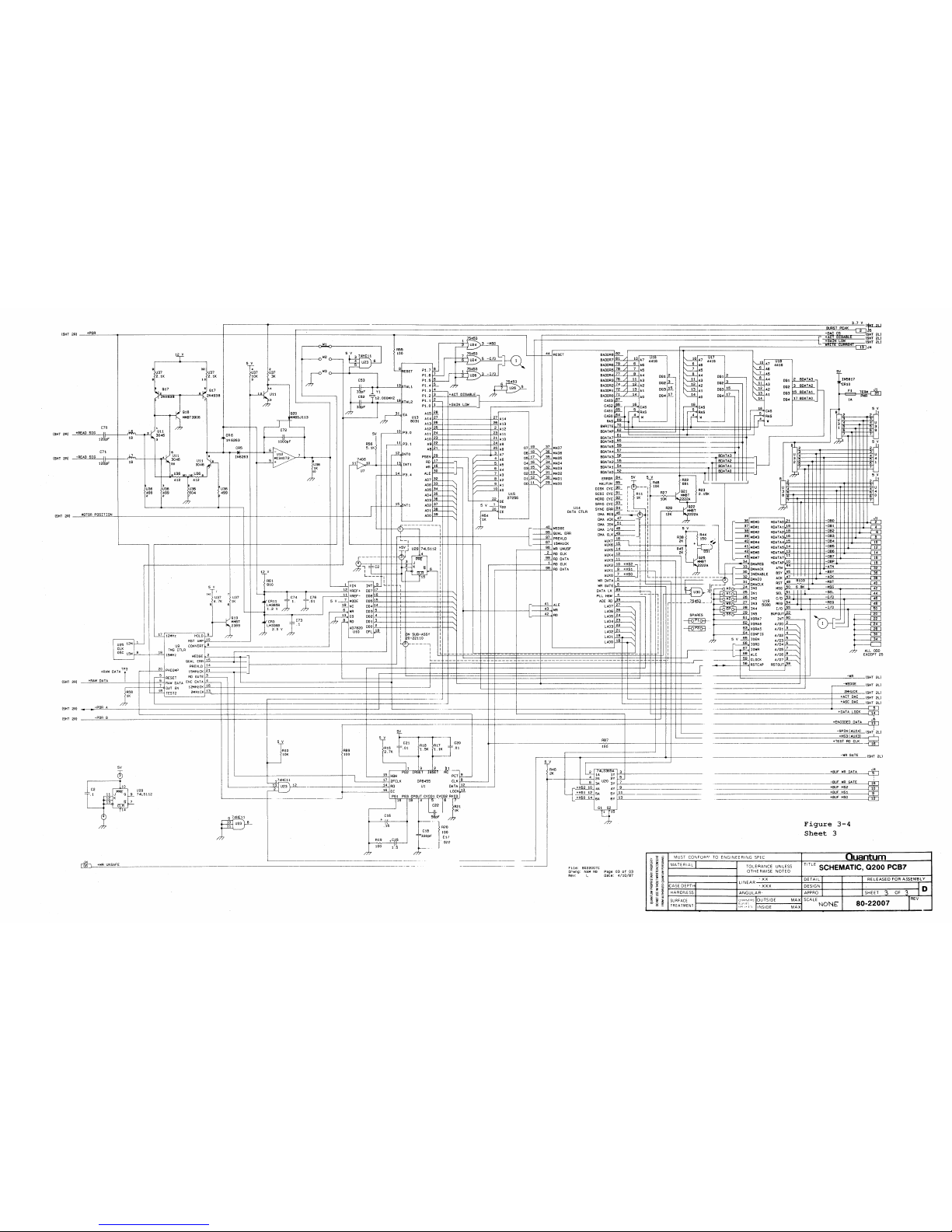
3.7V(~
BUAST
PEAK
~
Js
:~~f
B1sABLE
:~~i
~~l
-
-"~L------r-----------------------------------I=-=-=-=-=-=-=-=-=-=-=-=-=-:,~=-=-=-=-=-=-=-=-:r--:==---==--==--=:=""-<'=:=:=:=:=:=:=:=:=:=:=~~~~~:===I:"'======--=--=r====~~=~17~5-4~5~3)~_~~:lI
__
~-=-=:--=
__
\=~~-:=~============================================~======~~~;;;;;;;;;;~==================
___
[
wg~f~
E8~REN,~~~T
2L)
~
U24
3
MSG_
--------------~~~nl
r--ure--l
44
--RESET
BADDA8~
u.ID_
II
I,
10lA7
4U4\~
i~A7
4416
BADDA7
Bl / 10
A7
4416
l ---::-16 "
"6
I 5V
.~.
"-
m~,
J-Q
~-r--,-
I
~ 6 L~
A6
L~
A6
'1
ISHT
2R)
.
~
'"
',,,
I
'W~,,,
L..
" ,
.,
,,"-,--.,
"""
W2
5 V 3 7
4HC
11
~---'r-,,-
I"" ,
'W~,
"L
'.,
~
..
""
'-------,
~..
""
t'-"""'~
h
!'cAI0
'',''
t------<>
~
~"",
, " ,
~p~_
~'
m"~:
, -
'I"'
::::::
;;
,',
::
::
~
[:jt
::
""'
'-------,
Nt
::
""' , -:-:
::
"
----L"
~.
2
W3
O~--j
1----<>--------
I
r"~"
"
'"''
""~,
L'
~
.,
00'",-""
"
""'
c"--.
~"
"
""'
" " _
..
r
~
1
PI.5
6
~5
BADDAI
72
13
AI I
~~
1.0
DQ4~
\,,14
DQ4
17
BDATAO
,.
""
1:'"~
'"
" .
"'-
fl7""
""~"
"
..
'"
00'
R
~
_
' "
-'
"
,~,
'.
"
~
~
" G17 • G17
"l-~j..i".:W;-OQl"-----...§.t~
2N493 B
&12N4938j
Ii]
G18
MM8T3906
..
H.~ll
I
~.
G20
MMBSJ113
~f
3 pF
VI
PI2
~--
~.
________________
.
CAS2
~
~
CAS
~
RAS
5 V
1
re!,2
U 1'i3r------,.4'4
1
IU
ISHT
2R)
C70
+READ
SIG
12hpF
Mn
2
18"
1
.
Ull
3046
.
CA6
fiN
6263
,-----l
C72
~~
Jl
100DpF
F
1
Pl.3~+ACT
DISABLE]
CAS31':::::""
16
~
CAS
j]t
156
R
CAAS
S
'"
1"'"00"",,,,.~
'"
r,--.
..
,,"
'"
''''
"'-
,2."
• "
j4
W
Pl.0
LL_+
_
CASO ~ 14
W I
~
__
..
_
~
__
_
,""
",1
~':~r=-~6§9r~~i~~i~-~-~.~"~~~~~~~~~~~~~~~~~
31
A15~
27
A14
BWRITE
70
_______________
_
~
EA
U13
AI4.g-_
------------.--:2."61 A13
BOA
TAP
62
-=
.
".
~
~----------
/77
B031
AI3~1_
--------------
12
0
1
A12
61
A12
~~
r--"
23
All
~g:i:~li60~~~~
______ -____
_=__=__=__=__=_1~======::::--
..
____
"
V
12'"~"
,
..
" "
""
,""","
_.
__
--=-:-::-:-;;:
T
51
AIO
23 24
A9
37
1,§57...7 __________________
T
__
===__
BDATA3
}_
3 4 3
Il%
-i9
1 I
(SHT
2R)
U36
499
2
3
U36
499
2
f
U36
099
CR5
A56 ,----!l
P3.l
A9?
25
AB
~~~
:~~~
:~~~~:f-lE:566-----------------11--_==__---
-1-:B=D7:AT;:A-;;2TnT
...
,
,,"
......
"
"'~
"''''
'"""
"'
'=1-
1"1
BDATAI
I
~
NTO
PSEN
29 1
~5
AA65 04116
'I
ft
MAD4
BDATA1L5~4L
________________
I
__
_====
-l--rB""D",A~TA=OlnT
~
""'
"
r'
'"
""', " "'"
"
.-----.
I 1
~
1
__
10 13 INTI
:~
&3
6
0 ---
---
V
~
A4
02
113
'y::ll
MAD2
BOA
TAO
B4
5V
5 V R22 L ___
.-
_____
.:J
" 7
A3
01
~V
30
MADI
ERROA
r.::::-...,
"T
A48
681
"'
"
n.'"
v:::::::::::.:
'""Vi'
,~,~
~
r"'---,
,~
'"
07
32
~
A OD..!.!--. A
MADD
DISK
CYC?
Y I R27
L.-
~~~T
2.1~~
! I A
i33iU
1
""-----=-190
~O
1
" SCSI
CYC
J!L
1
Rl1 I -;
I
AD6
-;;-:;-
-~I
r
____
10
~
92
I lK I 10K
~22A
AD5
34
l-... 1
~
U15
MCRD
CYCr;;:;- I I
----
~--,--
--j
---
---
ISHT
2R)
__
~M02:!T].ORf!J'P'Q:OS§JIlITl'IO~N!..._t_----------------
,.. " . , " ~ '"''
'''"
'"
r¥.-
: ,
""
,~
4-,
AD3
36
I
U14
SYNC
EAA
~
,-_'=:-1
1
~22A
-DBD
,.,
"
~
'"
"m
""
""
~,
,
-{,
r
----"
~'""
_""
, • ,
5
V
,
"6
P1
12K
.
HD"TAO
21
~4
.-I-+-r--r-_
15
...,.
'" , ..
"
r~
~
"
""
'"
~
- , :
.~
,
",~"
~""
~1!..§94--l--I+H+H-~D;B~2t1TnIC:~1in56Ei
I
""
"
:1'
""
"'r¥---
II
, "
==§:~"
~""~1ll!:++-++H-H~~D~B~3t1IIII=--ip.;~ID
'1
----;:;;;
49
I I A38 150
~
-----:IQ
MEM4
HDATA4Wl~5--t-+-++H-nH~D~B~5t1lr===_~Il2=;lrg2E
ISHT
2R)
ISHT
2R)
ISHT
2R)
5 V
(}
J
:'1
[
U37
o
7K
,I
U37
lK
12 V
-,
A61
l
910
40
WEDGE
DMA
1/0
~ I I~
~44
39
MEM3
HDATA3
1 -OB4
'L=-.
"---1r--T
,£5
1
---------l:
-
~
GUAL
ERR
DMA
CLK~
I I
2K + .""
~
MEM5
HOATA5~1~4+H+H-t1+-~~tJ~======~-fT4Jl~4~
-,
~
"'~
'"u
lli:'l
' , )
~
Wl-?-3+H-MH-t1-f-~O~B6H-r~_===:n£
-----s7
15MHzCK
AUX6~
R45
42
MEM6
HDATA6111:':1++-++H--H-t-~D~B7pt_====
__
--m:::J
'
.-r-,.
"'
~~
'""
" ,
-t"
----..
...
,
'~"'"r,,g.0+H-MH-t1-f-~DB~P~--_=======-Q[JDli?:85
AUX41:~ _ M~~5T
-~DMAREQ
HDATAP~4
-ATN
------[1[]
~~"
"~
""'"
+'::
~~.
'""
"
""
~dJJ~3
DMAACK
ATN
~'~5:::~t~~::::~+~j;:~~B!:SV?::::::::::::=======_~-c3!D
,-----,-
J]J
3
J"; ,
""
~
'""~'~1L
: ,.!:, ''''''''
:::
~:!Z.7~A~I~0;3+~---:=~~~~~~----======mD!fQ:B5
lY.
~1-------"-----~---+t---------------TT--g:98~RD
DATA
~UuXx~~J:
rc:
___
_______
____
----;1
DMAIO
AST
~4~8--~;-f4----:-:;;M~SG~------:-:------QD=_-1=j4~25
4'l----r-:c:-t--t--r-I1~..J,
'c
_ I L+
=--
_~
~.'"
1~5~0--;-'6~''i'8K~>-
__
~:;m:-I-_
l!C~
I
'";,,
'I
::
:::;':
~ , ~
,Ii~~§==#
:::
::~
::H:P
::~~
---HE
L
DATA
LK 8 __
9___
,~-
~
:h~~
IN2 U19 C/O
54
11
-AEQ
O!J
I
VIN
,,,-,-,-,
~,~,
0.'9
_
__7J?~~_
.... 1
>--;ws-~
IN3
5080
RI/EQO 55
-l
-I/O
~
~----4~---T~-----~-_-_-
_
_=-=:.il_~l
VREF-
DD6~lL6-+++r-t----------ITI
[J-:
H
C
='
::
:~'
"
..
~,
~~"
~
~
~AA'
'"
~
I=-'-"
~
m",
",,/'
,
""
~
,
'"
~
~
'"
.~OO;
'"
B-c
rn::::
"'~--t++H----------rrD=
ADC
AD
~
, L
'i"El'
'i:l
2B
IN4
22
~~
~
I C74 C76 5 V 7
~ODE
D05~l£5--+-H:+--------=rITI~
-r---:-:--< LA05
~
'I
~
.....
______
Q6.2.
XORA6
A/DO
~3
128
* 1 T
01
'19
NC
j!.
14L
-l-++H----------rrfJ_'
~--+--t--r-I--
--"-
""
'"
,~
"---
1
.[ID
'~L~R3~~B
T d7' "6
WR
~~~""5'---t-,-'Tl11T
-
---.
t
r
" "
..
~
--@§l
!'-
~'"
""'~
,
.riJ
~
1.2
V
d7
~
CS
",'
1
~
""'~
"ro~,"
"'''E:'i
C'"
'
~--+-H++---------,:TL'
LA02 ~ 5 V
~
IDEN
A/D~
~
t--~
~
~,
-"
'"
T '
~""
e
""
"'-H~
67
IOWA
AlD5
r:------..
...
G19
I C73
l~
RD
DDOO~I<~~_+++:Irl-------
-1-
--
I
LA01~
/7'7--{_~
lORD
A/D~~
/77
EAXLCLEpOTDD2
;~,
r
""ffi
d,
, "'"
""
F'-
"
W.-.~,
: ,
,,_
~
..
~,
"".
~
1_,
~-'-
~
-~'
~~"::11~~~~~~ld~~~~~~~~~~iiiiiiiiiiiiiiiiiii~-f~~~~~J
-f~J~~~R~~
~~~
~~
L!2..j
12MHz
RST
AMP
'p'I
·"'0"_________ -----------------
--
,~.~li~'
t~t~~~*~~~~~-
_!~~~!~~=====~~~~~j~-
-~---~r~lrJrJ--JI~:
__
-_=
-====={~5~61=A=S=T=CA=P===R======r===fT=---------~~~-W;A~_ISHT
2L
U25
1~1
~~~-----
--
---------~l~~~~~~~~~~~~~~j~~~~~~f-~~{~~~~=~{JJ~~~l~~~~~~~~~~~~~~~~~~~~~11}f~1~~~
~~~
CLI<
19
15TMMHGZCTLA
,----]---
t-
1
osc
15Mt-=-...8
__
r--
__
._.
WEDGE
c=2
_______
t-
'-1-
1-_____________
--------------t--------;:===--f----t-------i="
_
,~'"
,~;~,
I
,
OO~
rnR,~
-.
C -
~~~====~~======~==~~~~~~~~~~==~~======~~~~~~~~~
_
_____
HU
O~
~~
2U
PAEVLD
>'1...,4________
II
lL
I
____________________
_====--_-
__
-----------
-----r---:-:-+
AGC
DAC
_ISHT
2L)
TP3
~--;-
__
20
,PHCO~P
15MHzCK
f-'2~1
_______
1rl
-
'-----__
____
...0:::,
~~T
~~U
~~~3~~~~i-tlt~~~~~~~~~~~~~~~~~~~~~~~~=-=-=-=======r=~=f~==~~====
+~~
~
1 '
•• " ",.
~
""&--.
., "
-
--.:+':.ER~AW~D~AT!.!AL----'-----I-__=D=z7jOUT
EN
12MHZCKI.I~6==r~~f_------------------::===========___
_
__ . _______
.ENCDDED
DATA
mJ
2MHZCK~3
-----
-..
_
-,
___ . ____________________
--'-"='~
__
__.- I
~
cT
__
ES_T_2_____
.-J
- -
_____________
-SPIN 1 AUXO)
ISHT;
2Ll
R58
IK
-POA A
-
-POA B
J
5
:10
10K
5V
§
LF
o
C2
I'RE' U29
=
11 J Q 9
74LSI12
.1
12
K
13
IT
7
ern
14
4
974HCli
~
Jll-
L--.--t-::-:::;:-:--;----
R89
100
- -
------
t-
5 V
~"v----T---T-·-···lc20
-,
C21
R18
AI7
J.Ol
:~I~K
Tal
1.5K
UK
~
r---
11
3 2
..
,!lel.-
PG2
IRSU
.B~c
PCT
~
~_---:15_
I
HBW
DPB455
CLK
r8~
__
_
L-
___
~17;_2FCLK
Ul
DATA~.
___
._
~15
A?O
RI9
t
C
0;'2
I 5 V
"l
R46
2K
"
R87
100
--
-
~
~.--
~'"74~~3+-----------------------
~~:
~~
~
----
~----T---~u~-·6;
131.
U20
3V~~----------_-~=----_==
____
_
+HS2 10
41.
4V
t-----
___
I
f+H'S1i2
5A
5Y
~
______ .
______
-_-_--_-
__
_
~~
61.
6V~I~3---------------
+HS3 1
AUX3)
[:=J
--------=::::::::::::::::=--::::-::::::::::::::::------------------~.~T~ES~T:A~D~CL~K~
_
_[l[]
(SHT
2U
--------------------------
-WA
GATE
+BUF
WR
DATA
m
--------------~~~
.
--
-BUF
WA
GA
TE
O!J
-~------
-
.BUF
HS2---------Cill
------.. --------------:;:.-;;;BU-;;:F=-
><H'S"1
-----C[:J
--------------
+BUF
HSO
c::ID
--
Figure
3-4
Sheet
3
~~+_WR
UNSAF~
L
CIB 100
J
330PF
ell
---
--
.---~-~~::
--
-
Fi
Ie:
B022007C
Drwng:
NAM
NG
------,--M-U-S~T-C~O~N~F~U~H:\~.
7T~O~E;N;G~I~N~EE~R~I~NGG~S;P~ECC----======][============~~J~U~~Clrrt~lJ~rn~~::~------l
~£
~R:
MAHRIALj
TOLERANCE
UNLEESDS
TITLE
SCHEMATIC,
Q200
PCB7
~ ~ ~
~~~~~============~~--~O~T~H~E~_R~:~~~S~E~N~O~T~~--tED~E2T~A~IL~====~~====~AELEASEDFORAS5EMBLY
Rev:
L
Page
03
of
03
Date:
0/10/87
§
~ i ~---:7::-r------------,
LIN EA R
'.X
X X
DES
IG
N
:I'
CASE
DE
PT H
APPRO
~ i ~
HARD~ESS
ANGULAR'
LE
~ ~
~
I-=0:....;U_T_S_ID_E
____
-;M::-A-;:X;;]
SCA
NoNE
g
~ ~ ~~~~~~~NT
'-.
INSIDE
MAX
OF 3
Page 51

=
~
=:
~
r--..l-aL=:Bil
1
-~ -
~
~
ASl
~
- R4C
--
_
~
_
:r
'"
<'I
RSJ
OS
"'"
- rn 1
C25 -
A49
-
Rt03
UE
U38
""
":."
...
Oil
r=- -
EI~I'
£1;
:
~o
U12
OW
::
!lIl
....
..,.
_ - § .. -
"'''
~
_ 1 LEa
~
au.
R5IJ
l.O
U4
0 - U37
LOO
~
en.
CD
_C62
a - -
-CSFU'!i
-
Am
U9
U41 U40 E14
-
CS7
- CSB - CS9
OJ
-
-
y
C48
-
1
.J1
Ul
U16
B-P~O
rr
Ul
-
~
RS6
_
II)
~
R56
a:
E&
F1
UlS
III
..
Ul.
u
UtO
1
Ul
-
~
-cJ-.
L·O
-
1-
CS9
~
-£:]-
~
D
-Q
-R99
os-Q
~~-
~
0<7
0 !
=J
a =
~o
~
- -
fi
_ R3 - RlO
_ 6 R15
L1C!
o
B -
c-JQ2o'1
81
-
~
c-ir
D -
!QL2i
-
~ -~
d:-
C56
~
~-
~
_ _
~
-
e:
..
_~-~N
u
D!
_~I&J-::
_
ij....
Ir""
1"1
U
D-U!=:I!=
~=:~
!=J-m
~
_u
R64 -
[) -
w-
_
RZ3 TP2 TPt
Lit
-
c::s
_ C4
- !
II:
-
~
I -
-
~
..
a:
-
-
..
u
CS4 -
El3
~:i=~=~OCRI
RiC!
.Jot
csa
-
~=
=8-
,,--
___
.1
~
~=---=-C&l
-=Rt8-=-E4~C2GI-
~-
~
QUANTUM
CORP
....
a
I
{\
-
I
(\
en
a
--
Q200
PCB
8-
SILKSCREEN
FA8
10-22008
ARTWORK
30-22008
RE
CRD
A0388
KRL
8 V 02
-6-86
Fi.gure
3-5:
Printed
Circuit
Board
Parts
Locations
Page 52

'ES:
UNLESS
OTHERWISE
SPECIFIED.
THIS
SCHEMATIC
APPLIES
TO
ASSEMBLY
20-22008
OF
THE
SAME
REVISION LEVEL.
ALL
RESISTDR
VALUES
ARE
IN
OHMS,
ALL
CAPACITOR
VALUES
ARE
IN
MICROFARADS,
ALL
INDUCTOR
VALUES
ARE
IN
MICROHENRIES.
R29,
100
ARE
NOT
INSTALLED
IN THIS
ASSEMBLY.
SHORTING
PLUG
OPTIONS
ARE
SHOWN
AS
FOLLOWS:
1'0
o-.!.
OPEN
CONNECTION
4-oL
SHORTING
PLUG
INSTALLED
I.
e.
OP8455
OP8464
DAC0832
EL2017
LM358A
LM339
7406
HA13426
TMG
CTLR
A07820
3046
MC34072AP
8031
DATA
CTLR
27256
4416
5080
74LS365A
LM358A
74HCli
75453
ose
220
ohm/
330
ohm
iIOOK.
ohm
74LS112
POWER
CONNECTI
ONS
REF
5 V
12 V GROUND
REF.
PIN
Ul
20
NONE
10.
19
Jl
01
U2
NONE
9
17.20
02
U3
19
20
3,8
U28
03
04
.~
U4
NONE
20
10
05
U5
NONE
8
4
06
--
U6 3
NONE
12
07
U7
14
NONE
7
OB
U8
NONE 1 5.7
09
U9
12.22
NONE
1.11
10
U10
7.20
NONE
10,
13
II
Ul1
NONE
NONE'
NONE
12
U12
NONE
8 4
13
U13
40
NONE
20
14
8.
17.25.33
3.13.20.
U14
50. 58.
6.8.
NONE
28.
38.
45.
75.
86.
100
53,
63.
73.
80,88
U15
28
NONE
14
15
1----
16
17
U16
18
U17 9
NONE
1.18
19
U18
1.12.
17,
23
20
U19
20,
49.
65
NONE
35,
46.52.
21
7.
61.
62.
64
U20
16
NONE
8
22
U21
NONE
8
4
23
U23
14
NONE
7
24
U24
8
U26
25
NONE
4
U25 11,
14
NONE
I 7
U31
I
U32
NONE
'NONE 1
U38
U39
U40 I NONE
NONE
U41
U29
16
NONE
8
CONNECTOR
PIN
ASSIGNMENTS
SIGNAL
NAME
PAGE
REF
PIN
SIGNAL
NAME
PAGE
REF
PIN
SIGNAL
NAME
PAGE
REF.
PIN
SIGNAL
NAME
PAGE
GNO
-DBO
GNO
-OBI
GNO
-DB2
GNO
-OB3
GNO
-DB4
GNO
-OB5
GND
-086
GND
-087
GND
-OBP
GND
GND
GNO
GNO
GND
GND
N/C
TERMPWR
-.-~
3R-
3R
JI
26
J2
01
12 V DC
IL
J4
01
ACT
COIL2
~
3R
27
GND
3R
02
12 V RT
IL
02
ACT
COlli
3R
28
_
..
".
':3R
lL
-
GND
03
5 V
RTN
03
FIL
12
V
...
_-
3R
29
GND
3R
04
5 V
DC
IL
04
GNO
3R~
30
-
.-
GNO
3R
05
'BUF
WR
DATA
..
_.-
3R
31
GNO
3R
06
+WR
UNSAFE
.---
.-
-~
3R
32
-ATN
3R
07
GNO
-
..
-
3R
33
GND
3R
08
FIL
5 V
_.
.
__
..
-
3R
34
GND
3R
REF.
PIN
SIGNAL
NAME
PAGE
09
+BUF
HSI
-_
..
.-.--.-.-
3A
35
GND
3A
J3
01 HALL
GND
2R
10
+BUF HS2
--
3R
36
-BSY
3R
02
HALL 1+
2L
11
ROX
--~--
3R
37
GND
3A
03
HALL 1-2L
12
+BUF
HSO
_.
---
3R
38
-ACK
3R
04
HALL
2+
2L
13
WR
CURRENT
..
---
3R
39
GND
3A
05
HALL 2-2L
14
ROY
--
3Fl
-_.
- ... -
40
-RST
3R
06
HALL
3+
2L
15
GND
----
--
3R
41
GND
3A
07
HALL 3-2L
16
-8UF
WR
GATE
-_
......
.--
3A
42
-MS6
3R
08
HALL
12
V
2R
-~
-
--
3R
43
GNO
3R
09
COIL
A
2R
REF.
PIN
SIGNAL
NAME
---
3R
44
-SEL
3A
10
COIL
B
2A
J6
01 LED AETURN
45
•
__
0.
-3fi
3R
GND
11
COIL
C
2R
02
LED
SOURCE
3R
46
-C/O
3R
03
LED RETUAN
-
3R
47
GND
3R
.-
3R
48
-REG
3A
--
3A
49
GNO
--3A
50
-I/O
3A
.~-
L11
FIL
12
V
J2
12 V DC
~
::
"
01
~
........
--_~-----<-_----------
12
V
::
BEAD • -C3B.
CB • 28.
37.
64-66.
l.J!!0~0
_____
..,-
___
~14_05_.
_49_._~
__
-+-
___
---,T
.1
75.
91.
93.
12 V RTN
5 V
DC
5 V RTN
GND
10
J2
L5
Li2
4.7
J4
08
FIL
5 V
:=L
J~
04
.~_-J"'L-
__
.~
___ ~ ___
~_-+-
__
5 V
BEAD
C46
22
C44
.
01
C3.
19.
25.
33.
34.
47, 4B.
50
.1
51.54.55.67.
6B.
69
.
~
07
15
GND
Fi
1e:
B022008A
2R
2R
IR
IR
3R
3L
lR
IR
3R
3R
2L
3R
2R
3A
lR
3R
PAGE
3R
3R
3R
Drwng:
E.M
Page
01
of
03
REV. F
Oat.:
04/8/B7
REF.
PIN
SIGNAL
NAME
PAGE
J5
01
C
AGC
2L
02
8URST PEAK
3R
03
SET
HYST
3L
04
OET
REF
2L
05
-WEDGE
3R
06
GND
lL
07
5 V
IL
OB
12
V
IL
09
12
V
IL
10
5 V
lL
11
GNO
lL
12
N/C
13
+ENCDDED DATA
3R
14
+DATA
LOCK
3R
15
N/C
16
+TEST
AD
CLK
3A
MUST
CONF(lHM
i
~
MATERIAL
i
~
~
~
~
I
CASE
DEPTH
'"
HARDNESS
:>
~
SURfACE
0-
TREATMENT
TO
ENGINEERING
SPEC
TOLERANCE
UNLESS
OTHE
RWISE
NOTED
LINEAR
.
XX
".XXX
ANGULAR-
~8~~~RS
IOUTSIDE
MAX
B".""
IINSIDE
MAX
Figure
3-6
Sheet
1
Quantum
TITLE
SCHEMATIC,
Q200
PCB8
DETAIL
I I
RELEASEDFORASSEMBLY
DESIGN
I
I J
D
APPRO
I
I SHE ET
I
OF
2>
I
SCALE
80-22008
IREV
NONE
Page 53

ISHT
3A)
(SHT
3A)
(SHT
3Ri
(SHT
3R)
(SHT
3R)
(SHT
3R)
(SHT
3R)
ISHT
3R)
ISHT
3R)
ISHT
3R)
ISHT
3R)
~-------:-=-=-=-=-=-=-======-:-~=-=-=-=-=-=-
__
-=-=-=--=-=--=-=-
_-
___
-=-=-=-=-=-=-=-=:::-=::::::::::::
__
-_-~_-_-_-_-_-_-_-_-_-_-_-_-_-_-_---------t--------------~----------------------~------~_-_-_-_-_-_-_-_-_-_-_-_-_-_-_-:::-:::-:::-:::-:::-=:::-:::-:::-:::-:::-:::-:::-:::-=:::-=:::--:::-:::-:::-:::-:::--=-=-----------=:;:~~~:~:~t--~
:~~~
~~~
I .
_________________________
~----------------------
.
_______________________
~+P~O~A~___
(SHT
3L)
~----------------------~----+-----~-I------.-
5 V
A2
51K
5 V
R67
390K
5 V
RBO
2.15
K
5 V
5 v
U33
lK
HA1342B
UB
U
13
v
IS
W
17
':l
~~~~5B
13
7 +
Q27
~l-------
.---[
~!
~~
_______
1~9
+w
_..
18
-w
LIMIT
~1!...1
~R",97~-,
.
24
1
CR21
SDI03C
1.245
V
5 V
- 9
-lu33
I C27
.~.01
~7
14
R6B
390K
U5
6
LM339
>-1~__1O__--_-_{-loo.
~~~!
R62 Y
~~BT
---+-~B~.2~K---I
3904
C24
.22
RB3
750
~=-=-=-=-=-=-=-=-~:!~gl;
r
~
~-----'-'::'-i
015
II:~ 2 MUC13~072
I
r-
___
~4_1
~~:
I2----l'-"~-,
3
AP
r-
___
--=5c..,
012
~
___
---:6,-,
011
r-
___
--'-7-1
0IO
A70
504
RBB
..
_ ...
____ ~ OSC
IN
.--------w.1---7
~:~N
OUT
r
1.
BK 3 SOBIAS[-p=J
r---""-'I>r"-
I 5
MOOE
v r
~
SDr~o
'"
I"
~
C35
R95 R96
8.2K
1.2K
12,V
R9B
NC
~
27.4K
I 267K
I C42
RB4
1.
7.5K
.d~8
3.6K
r-
_____
-=-19"-j
ILE
__
...!+~A§.!GC'_.Q.OA~C'__~
_____________________
__t.//
I
CS
DA~~~32
12
1
:
39
....
___
___<_~-----....:;.R4~0~----__{v
~~2222A
1.6K
......
-I-_Av49~
__
-fV
~~ciT
12K
3904
~WRI
P
IB
WA2
17
XFER
WREF+VREF-
~
ICll~O
____ ~ ____________
~
740B
_____________
~13~
12
__
.~G~A~IN~LillOWL_~~-----------------_+-i-i------------------t-
__
--::::::::::::::::::t=t:::t:::J----.--
U7
_~2~MH~Z~CL~KL_~
____________________
_t-t-t---------
---------------------+------------+.-r-~
MAD
0-7
,----------------
------
J3
HALL
1+
r;,C51-
9
L9p, -rc: l 9
-~
HALL
I
T~~~
l'-~
017
2 _ 47pF
L..C!.f-J
.L C31
--------.-------+--+-----------------.-----+---------f---J
"----.!..2...
015
II
LM358A
..
~
i
HALL
2+
T·
OI
~OI411~~12o......---<~3'--!+U21,/.·
'U34
~
HALL,-=:3-=-+
__
~-=-c----
~
013
12
10K
12
V
R6S
10K
CA4
~MBD914
Rn
3.3K
......
__
-0+-"
Q
II
-I
MMBFJ175
r-
SELECTED
.U34
9
10K
CR7
CRB
R51
SDI03C SDI03C
2.2
R52
2.2
R53
2.2
C39
'=
C40 C41
"
.1
r=.1
".1
AB6
7.5K
G3
3904
R36
12K
C60
I~
1·-:·;;·6'22
110K
AB5
4.7K
1M
CR20
SDI03C
I
EL2017
CR2
SD103C
-I G15
~
MJE200
R206
360
R43
.5
U4
(B)
PNP+
~f-
VOUT
-!-=4,---+_...J
!
NPN+
1-'3'--.-+
__
-,
o U35 •
12.9K
12
13
~
HALL
2= J "-......!i.
016
~
1:
C32 i'----'L
012
• 6
'
=r.
01
"-~
OIl
......
---l-----
...
~-"--i-
7
~
HALL
3+
~
010
8
U34
R69 5 +
U5
_.c::+A~C,TL...!O~A~C
__
_I_-------
---------------------+-+------
-------------.-+---------..
-.--.-t-
.. --.....
-.-
.....
--¥-
ILE
U3
20K
200K
LM358A
__
.:-~DA~C~CS~_-i-
______ . ___ . ________ . __ . ____
~_+_------------.-------t--------t----_
~~~--=-::-----.-
..
=t
~:~AC0832
EL2017
141
I
I
NPN+
(D)~
C62
Cc
+ S I------,
~
__
-t-=-14.:..,
~
0022
m
~
PNP
IB
U35
100
VOUT-·f.:1!.;;6'--~---
NPN~
__
.:-~WRL
__
___jlf_,
------c;-:;;;::-------:-----
--------+---------------
--.-
plB
WA2
~
7406
8 5 V
12
V 17
XFER
RI2
U7
3.65K
I fJREF+VREF-
A3
9
10K
lU\1
~7~K ~7~K
r I
QIO
I
);
10
10
~
~::D914
......
_____
-+
___
-~9'iyIIU27
rth-J..:o5::!W'£E!!!DSG~E:~H-YS-T--j--t-:~'
..
-'"
1
_______
:7~:_K
___
_"_{6
~
..
:-U2-7--.=.c12=-J
14U27
3~l-62.4
__
~-'2'4J:-
~.
+,.;~,I
:'i.
J"
I"':
J'
-
~
~----~~
h
MBT3906
R77
2.0K
6 _
m-
....
LM35BA
7
5
V
_5
+
U21
A76
I.BK
U35
0.5K
U35
s.IK
u41AI
NPN-(D)
~
CC-
n
•
"'S:=ELTE""6C"-T-1P'-iW~~C...J'1
I C63
::~5
~J~~60
1
U34
2 J U34
40K
2
10K
].0022
u:-I"
--+------'
.............
,I
oU34 •
LM35B~.
··..--.L-
IOAK
....i..--+-----·-----1
.
U34
40K
.
8 _
EL2017
11
R42
.5
3.7V
-----·--------------------t-+-------------t--------
~----~-------------------~--------
U41CI
7406
~+~A~CT~D~IS~A~BL~E~-----~3~
4
l
ri
----------
_._--------._---j----------+--_.
__
._.-
U7
TPI
C4
I
READ
x
rJ~4~~R~DX~--~----_____1~1
____
+_----.-+.------
UL1
.0022
TP2
J4
ROY
J5
DET
AEF
A24
511
AI.
IDa
1
READ
Y
C5
T·
I
t.----------'
6 18
7
U2
(AT>
19
DP8454
1
.......
-----------------_.----_._---_._-
..
A5
lk
A6
130
12V
-.--
......
--------1r-----.
A6.
365
A7B
365
__
~
___
_+-~-~--IV:0~B--------------+--~-M+MM-~.-~-3'.-M--~
L--.
______ . ____
.
IC5
-L
5 v
____________________
-+-
_______________ .
__________________
..
__________
...
__
.
---_.--------
..
..
_.------------
CAGe
.~?---
.luF
--
~CI
200
T68
P
F
1
~4
----------------------_._-
----------
--
COIL
A~
COIL
B
..FT5l
COIL
C
..r==ITl
J3
12 V
---t:Q!]
CR22
lN4001
CRI5
lN4001
A T COIL
1~
,"CA1S
lN4DOI
CR13
IN4001
J4
ACT
OIL
2LQLJ
CRI4
IN4001
-READ
SIG
(SHT
3L)
+READ
SIG
ISHT
3L)
+RAW
DATA
ISHT
3Li
7406
1~~5
--------------------t-----
----.--------
-----
---------------------
ISHT
3R)
__
..::!W!!:!R...!G~Ac!:TE"__
___
---,,-<05t>>-...E6--......
------------------------+-.-----
_____________________
..
__ . _________
_
...
------------_.
.
__
.------._----------------------------_.---------
Figure
3-7
Sheet
2
U7
Js
CAGe
[QIJ
••
._.
_ ...
_._-----------
C9
R9
~
__
20K
FILE:
80220088
DRAWN
BY:
E. M
REV:
F
SHT 2 OF
3
DATE
04/08/87
~:M~U~S~T-C~O~N~Fl~)~"~~1-T~O~E~N~G~I~N~E~E~A~IN~G~S~P~E~C
____________
~~~---------c:l::~llJEi==~rtt~tJ~fllww~-------------1
MATERIAL
I
TOLERANCE
UNLESS
TITLE
SCHEMATIC,
Q200
PCB8
OTHERWISE
NOTED
CASE
DEPTH
ANGULAR·
HARDMSS
~-------r------------~LlNEAR--·:X:X----------~~D~E~TA~IL~-----+------~A~EL~E~A~S~E~D~FO~R_A_S_S_E_M,B-L-Y_.
,.xxx
DESIGN
D
APPRO
SHEET 2 OF
3
SURFACE
1--
_____
-1
i?,~~~RS
OUTSIDE
TREATMENT
bR.,."
INSIOE
MAX
SCALE
NONE
MAX
80-22008
Page 54

Page 55
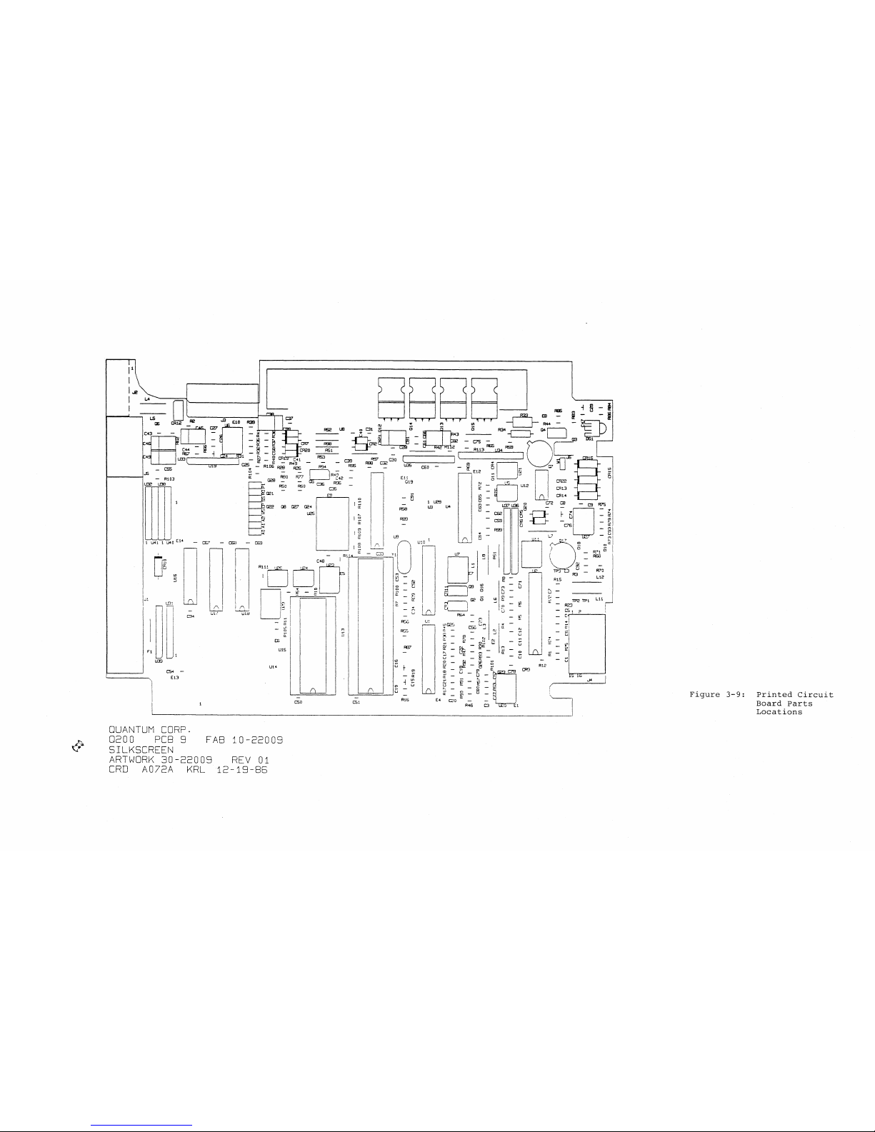
-
...
-
a:
=
~
:=
~
1 -~ -~ ,
0'l20
_ ~ _ ~ CR_
C41
cas
_
R10~
- R49 -
~
R2l3
R25
R94
~
-
CE9;0
~
IIR4~
__
~
c.+2
RSO
RSO
c::£
Fa;
eEl
C35
_ CS5
-
RI03
U32
LOO
C39
R$
FB3
RS7
C32
ao
~
_________
Il
___________ __
U3S
eso
-
~
E'
•
019
1
LE!3
E12
~
-0
U12
D CR22
_ 0'113
8 - . .
CRH
\J1
5
§ _
U37
l!E
0
C72
CE
_
~
_
-CSR7S
5-=
~
~~
~~Dn
O
U7
~~r
DO)"
1i=:~/
1
LH
1 1 lJ40
E.14
R58
U3
LH
R89
U!C
1
I
O
~
,5
tD
I
:5
CS4
-
E13
-
csa
-
CE9
I
LJ
I~
Ull
~
I
R!
'4
I
I
I
I
I
U15
U14
-
C3J
I
I
I
I
I
n
ID
U
O"l
.
-
("I
U
T?3. ~ - R70
C]09
5 I
~
=:
5
"15
R3 -C12
a
~
~
_ D -
TP2
lFl
LH
R23
8
ICE
-I~-~
~-
'-
R&4
_ u -
U!
- 8 -
!£
U
1
:=
~!
?
.---, ~ C2S
t...
I
R: ~ '::"
~
~ I ~ = ~
-
!.
~
=
~
~
t
=:
~
~
- ; I
~
~
;1
_ P r
~-
f :
~DC7B
"'"
""
/
cs!
Rib
-
&!
- - !
-:~~~~
__
~
____________________________
~~
________
~
____
~E:4~~~O~=-~~~==~
____
~:===
QUANTUM,
CORP.
"<6
03,
I I
0200
PCB
9
FAB
10-22009
u
cso
SILKSCREEN
ARTWORK
30-22009
REV
01
CRD
A072A
KRL
12-19-85
Figure
3-9:
Printed
Circuit
Board
Parts
Locations
Page 56

rES:
UNLESS
OTHERWISE
SPECIFIED.
THIS
SCHEMATIC
APPLIES
TO
ASSEMBLY
20-2200B
OF
THE
SAME
REVISION LEVEL.
ALL
RESISTOR
VALUES
ARE
IN
OHMS.
ALL
CAPACITOR
VALUES
ARE
IN
MICROFARADS.
ALL
INDUCTOR
VALUES
ARE
IN
MICROHENRIES.
R29,
100,
111
ARE
NOT
INSTALLED
IN
THIS
ASSEMBLY.
JUMPER
OPTI
ONS
ARE
SHOWN
AS:
.!...,
~
OPEN
CONNECTION
~
PUSH-ON
JUMPER
INSTALLED
I.C.
DPB455
DPB464
OAC0832
EL2017
L~358A
r-L~339
7406
HA13426
T~G
CTLA
AD7820
3046
~C34072AP
r'
8031
DATA
CTlA
27256
4154
4416
5080
74LS365A
LM358A
----
74HCli
75453
OSC
220
ohm/
330
ohm
100K.ohm
74LS112
POWER
CONNECTIONS
REF
5 V
12 V
GROUND
Ul
20
NONE
10,
19
--
U2
NONE 9 17.20
U3
19
U2B
20
3.8
U4
NONE
20 10
U5
NONE
8
4
.
--
U6
3
NONE
12
U7
14
--'NoNE
f--]---
U8
NONE 1 5.7
U9
12.22
NONE
1.11
Ul0
7.20
NONE
10.13
Ull
NONE
--~NE
NONE
U12
NONE
B
4
U13
40
NONE
20
8.17.25.33
r---
3.1~
U14
50.58.68.
NONE
28. 38. 45.
75. 86. 100
53. 63. 73.
80. BB
--
U15
28
NONE
14
--
U15 B
NONE
16
~:~
g-
NONE
1.18
1.
12.
17.23
U19
20. 49. 65
NONE
35. 46. 52.
U20
16
NONE
~.
51.
62~§.i
U21
NONE
8
4
-
---
-----
NoNE
------
U23
14
7
--
-
9
U24
8
NONE
U26
14
--
-
U25 11.
NONE
U31
U32
NONE
NONE
U38
. .
....
_-g
U39
U40 1
NONE
NONE
U41
--c--
U29 16
NONE
B
_
..
~-----
--_
..
-
---
REF.
PIN
SIGNAL
NAME
PAGE
Jl
01
GNO
3A
02
-OBO
3R
r---+-0-3-+---G-N-0----~
--
04
-OBI
3R
r·---r--4------r-~
05
GND
3R
~--~--+----------
06
-082
3R
07
GND
3R
08
-OB3 3R
r----rO-9-4---GN-D---r-3R~
r----+-l-0-r---~D~84---~
----+-~
11
GNO
3R
f---+-l-,-2-+-----,0~8-=-5
--+-::-3R::-1
13
GNO
3R
_
..
_--1-----
14 -OB6
3R
r---+--+-
15
GNO
3R
16 -OB7
3R
f---+--+---------r---
17
GND
3R
f----+-1-8·+-------0-B-P---~
19
GND
3A
r-----+--r-----+_~
20
GND
3R
r----+-2-1-+---G-N-D
---+-::-3R::-1
22
GND
3R
23
GND
3R
24
GND
3A
c-----+-2-5-+--N-/~C----r-4
L-_-L
__ L _______
L---
J5
REF.
PIN
SIGNAL
NAME
PAGE
Ji'26
TERMPWA--3A-
_._-+--+---------_
..
---
27
GND
3R
-----
28
GND
JR
----
29
GND
3R
..
--
30
GND
3R
---r·--r-----
..
--
_
....
-
31
GND
3R
--.
1----1---------_
...
_--
32
-ATN
3R
33
GNO
-jli-
r---+-3-4-+----GN-D----·
JR
35
GND
3R---
----
36
-8SY
3R
f---+~3~7--t----'-GN~D-'--
iR-
_
..
_----_
... -
--
38
-ACK
3R
--r----i-------
---
39
GNO
3R
--
._-
._
... _
..
_-_.--
.......
40 -AST
3R
----'41
--G'fio---jA'-
42
-MSG
43
GND
44
-SEL
f---+---r---
-
3A
--
JR
-
jFi-
45
GND
JA
46
-C/O
-JR
--r·-r------·
-
.. --"-
47
GND
3A
48
-REG
3R-
......
-
49
GND
JR
r----+-
5-0
-+----
I
/.,..0--
..
-. 3R-
'--_--..1
__
--'-
___ . __
........
___
_
CONNECTOR
PIN
ASSIGNMENTS
REF.
PIN
SIGNAL
NAME
PAGE
J2
01
12 V
DC
lL--
f---.-+---+---------
02
12 V
RT
lL
-
03-
-'5V
RTN--"1L
-_._.
__
...
_--
04
5 V
DC
IL
,--._-,--,----_.
__
._-
REF.
PIN
SIGNAL
NAME
PAGE
----:;3'0;-
-HALL
GND
2R
f---+--+----.-.---
02
HALL 1+ 2L
-
03--
'-HALL1:--2L
04
HALL 2+ 2L
---
--
-------_._--
05
HALL 2-2L
-
_._-_._
... -
--
06
HALL 3+ 2L
07 HALL
3-----'a-
----~-------
..
--c--
08
HALL 12 V
2R
f---+---+-
09
COIL A
2R
-'-+-1-0
-+-C-OI-L-B -2R
-~--
c---
11 COIL C
2R
L-_-'-._~
______
.
L..._
~PIN
SIGNAL
NAM-EPAGE
f----+---+-----------+-----
J4
a 1
ACT
COIL2
2R
r----+---+-------------
---
02
ACT
COlli
2R
03
FIL
12 V
lR-
r---+--
-----
-
04
GND
lR
05
+BUF
WR
DATA
3R
f--_+--+--
06 +
WR
UNSAFE
3L
07
GND
IR
~---+----+----------------
08
FIL
5 V
IR
09
+BUF
HS1---~
10
+BUF
HS2
3R
II
ADX
2L
12
+BUF
HSO
3R
13
WR
CURRENT
2R
14
ROY
3R
15
GND
IR
16 -BUF
WR
GATE
3R
L-
__
--..1
__
-L
_____________
____
REF _ PIN
SIGNAL
NAME
PAGE
J6
01
LED
RETURN
--~
02
LED
SOURCE
3R
03
LED
RETURN
3R
L11
J4
,-~-----CQIJ
I
4.7
FIL
12 V
12 V
DC
:--l
~
CQIJ---
BEAD
..
~------<t_---~---+-~------------
12 V
12 V
RTN ~ _____
_
5 v
DC
L5
------+-~
8EAD
C8
, 28. 37,
64-66,
.
__
---
J
.1
75.91.93.
1c46
IC44
112
~
I CJ,
19.25.33.34
47,48.50
FIL
5 V
5 V
5 V
RTN
CQD-
__
---+-_-
___
-'
I 22
TOI
r
""""'i~'~
GND
J5
GND
[Q§:J-.
15
File:
8022009A
Orwng: E.M
P.ge
Olaf
03
~EV.
C
O.te:
4/28/87
REF.
PIN
SIGNAL
NAME
PAGE
J5
01 C
AGC
2L
02
BURST
PEAK
3A-
f---+~0-=-3-+--'S:-::E=-T-,H=YS~3L-
04
DET
REF
-----a-
05
-WEDGE
3R
---
r-~-------+--I
06
GNO
lL
07 5 V
IL
08
12 V
IL
09
12 V
IL
10 5 V
lL
f---+-I-I-+----G-N-O-----+-l-L--
12
N/C
--
13
+ENCODED
DATA
3R
14
+OATA
LOCK
3R
15
N/C
16 + TEST
RD
CLK
3R
MUS1
CONF()I<'.I
TO
'"
~
MAHRI"'l
~
-
!
~
~
!
CASE
DEPTH
:0
HARDM~S
=>
~
=>
~
SURfACE
TREATMENT
ENGINEERI\G
SPEC
TO
LE
RANCE
UN
LESS
OTHERWISE
NOTED
·xx
LINEAR
.
XXX
.'NGULAR·
:'.;",~:
~I',
IOurSIDE
MAX
..
" .,.
I'\S'OE
MAX
Figure
3-10
Sheet
1
Quantum
TIT
L E
SCHEMATIC, Q200 PCB9
DETAIL
J
J
RELEASED
FOR
ASSEMBLY
DESIGN
I
I
ID
APPRO
I I SHE E T
I
OF
~
1
SCALE
IREV
NONE
80-22009
Page 57

Page 58

BURST
PEAK
3.7
V
[~
~~~¥
ghABLE
IT:i~~T
2L)
1+----------------------------------------------[
+GAIN
LOW
(SHT
2L)
(SHT
2RJ
l-~~+~PO~R~--------------------t--------r~---+-~~~~~~~~~--
____
~---------~-~~-~~~=========
NOTE:
R7
IS
NOT
USED
75453
ON
THIS
ASSEMBLY.
~
+.J2V
U37
2.1K
(9)
U37
2.IK
~2
11I7
"
GI7
o1-,...,2=N""49=3=8J
......
-----..!!.·-t..r
7
2N493 B
G18
MMBT3906
C70
[SHT
2RJ
+AEAO
SIG
~
_ 2 V
'UII
-+--+~~~'---1~201~p-F---fl"8~·~~
~;046
I
-AEAO
SIG
C~1
~
4 V
·UII
UII
r-".
SHT
2RJ
-+-+~~~~--j
~--J'Ii"iB'Y'L--iI---t---+!...(133046
120pF
3046
L-~~.~UV36~6~.~U3v6~.U7
U36
:99
3
U36
~99
412 412
9 U36
504
10
U36
499
~
RI14
R55 U24 3
-MSG
5;!.
CA5
IN6263
4
U37
10K
3
2
U37
3K
G20
1 MMBFJI13
~L-
C72
1200pF
6 _
! -
~
IM~j~O~
7
~
5_IK
~V
lOa
75453
L-+--I-",44'-1RESET
RIOO
374HCII
7 /
~
~
~
L.LJU24.5 -CO
. 1
o
OHM
4 U23 6
~_
R7
i
~
L...i1~ESET
PI
7
~
75453
o
OHM
I
PI:6~'-
~
U26 3
-I/O
R29
PI.5
fL--J
t--O~O~HM--'
L
________
...!1~9
TAU
Pl.4~_
P1.3~
U36
IK
.0
......
________
~1~8
TAL2
~
3IEA
UI3
8032
5V,.. ~ P3.0
RS6
5.IK
.......R
NTO
11~6
~'>o'1",0"""_1-I-+----'-13"<l
INTI
U7
.-+-+-+-.!.:
14
'-l P3 . 4
PI.
2 3 +
ACT
DISABLE
Pt.1
~._.
PI.
0
I-I
...
_+-++.:..:G""A""IN"---"L",,OW,,--_.J
A15~
AI4
27
27
A14
AI3
26
26
AI3
A12
25
2 A12
All
24
23
Ali
Al0
23
21
AID
A9
22
24
A9
AB~~I-+~--------------1-2~SAB
29
,-_-+~3~
A 7
PSEN
-"
..
-
f----
4
A6
AD
pl.?-
t--I-:-}
WR
~f-+-
5
AS
ALE
~O_t-I-_
6
A4
~
__
7 __
A3
A07
~Lf-~
8
A2
A06
~Lt-",
9
AI
A05
~~_
f-~
10
AO
U15
IS
NTI
L.f
___
",22=.,J
DE
27256
07~
,..R
MA07
06~~MAOS
05~~HA05
04~v;;-
HA04
D3~
~MA03
02~v-¥n-
MA02
Olh~MAOI
OO~pMAOO
BADOR8~
r----,U,.1.r.o--6-~
BADDR7
81 9
A7
4164
BADDR6
79
13
A6
BADDR5
78
10
A5
BADDR4
77
II
A4
BADDA3
76
/'
12
A3
BADDA2
74 6 A2
BADDAI
72
/ 7 AI
BAODAO
71
/'
5
AO
CAS3&~
~A7
~A6
f'-.-2.-
A5
~A4
~A3
~A2
~AI
~AO
OGlt-L--
DG2~
OG3riLOQ4r!Z-
I'---
A7
~A6
i"-l-
A5
I"---!Lu
I'J.!.
A3
~A2
~AI
~
U1e
4416
OGI 2 BDATA3
OG2 3 BOATA21
OG3
15
BDATAI
OG4
17
BOATAO
WAItE
CoRRENl
(SHT
2L)
LTIJJ4
LED
RETURN
J6
LED
SOURCE
~
5V
IN5B17
<-CR10
FI
IA
TERM..r4s,
pI/A
CAS2
~ I ~
CAS
~56
CAS
CASI
~
~
RAS
r-"--<
RAS
11%15
4
6
CRAAS
S
r---a
220/330
5 V
CASO
~
t W I W
•••..
___ . ___
2 2 I
AAS
p-§.L
~____
_
r..
10
U
r;3<----~3
~
BWRITEll70E!~~~~~~~~~~~~~:~~~~~UI~tl'------....J
3 h4.---.-H--r5
4
~
0
BOAT
AP
62
I 6 6 9 K
:g:i~~
:~
..
-=====I=1=l:::t----'
r---;:=======~
17
'-
8DATA5~59:---
_______
-,--~----
'll
2 5
~
BDATA4r:-57:-
________
~--------.----...
20/
13~~~!§~~~~1112
I
BDATA3t--='56=--
________
-I
____
.. _
..
_",B""0""A-,-,TA,,,3++++_-
1
~30
u 4 ! U 0
BOATA2
55
BOATA2
~f-
3
r!r
5 4 0
BDATAI
t--='54-'-
________
-I
_____
..
H-l--'B""0"'A.:..:TA::..:1'-+-H_+_-
2 7
~
I K
BDATAOr52=---
________
-:lI
___
---<~++-I-"B!!!0.'!.AT!.!A~0++-++-
J I L
ERROA
~
5V 5 V R22
l.1
I B 2 5
~
OI~~L~~~~
~~~
6BI
R23
UI13~~~I~~~~g~~~I~~3:
U
~
SCSI
CYCf-'1-!-
All
......
_A-'v2"'7_-fV~~~T
2.I~K
31~
5
40
MCRO
CYC~
IK
10K
222A B IS 6 0 K
ISHT
2R)
-r~~MO~T~OR~P~OS~I~T~IO~N~----------------------------------+---~-+-+--------------
________
+-+-+-
__
~-----I
AD4~f-~
A03~_t-~
A02~f-~
AOI~t-""'"'
AOO~_t-~
5 v
-.L
Vpp
20
CE
R54
IK
UI4
DATA
CTLA
~~~~
~~~
~
A2B
jM~~~~
220/330
17
7
<-
DMA
REG
p:
4
0.::6:-_
...... _ 12K 222A
OMA
ACK~
36
HOATAO
21 -OBO
~
12V
R61
910
OMA
IEN~
t-t_I--+----,-----t--
'~
MEMO
_OBI.....L.
OMA
I/O~
5 V
1---"-':
HEM I HOATAI
19
r--;;-
DMA
CLK~
R44 I ~ MEM2
HOATA2
16
-OB2
~
AUX7~
A~~
150
L--1~HEM3
HOATA3
16
-083
r==r
AUX6f-!!L,
~'----~-+-+_-----1
...,
I
~
MEM4
HOATA4
15
-OB4
Frr=
AUX5
114
~
R45
w~·
'I#'
1 ~ HEHS
HOATA5
14
-OB5
'12
AUX4
12
2K
1 I
~
MEM6
HDATA6
13
-OB6
~
AUX3
11 .,
.~
L~3443
MEM7
HOATA7
II
-OB7
Ts
10 +HS2
HOATAP
10
-OBP
~IB
AUX2r::---:-:-::-:-~
Q2~:'--=n~3
OHAAEG
44
AUXI
~
I---
MMBT
DMAACK
ATN
-ATN
~
AUXO 7 +HSO
2?2A
~
INENABLE
BSY
p:4"'5+H+f+~.......::-~B~SY'---_-______UD
~R
DATA
5 I ~ OHAID
ACK
p:4':-7---;5~.-f-t~--=-:!CA~CK:_-----...{;=;;:;;=J3~8=
'------'-
VIN
INT~
WR
GATE
6
~_
_
_~
OMACLK
RST
4B
RI03
-RST
~
'------
-_~
WEDGE
,-----1---
-~
GUAL
ERR
--+-1--_+_-+-+----------
-t--22-
PREVLO
~----+t_H---_+----
_-t----!l2-
15MHzCK
5V
U29
74LSI12A
,--
___
f-
9
""6'-J
lOR
UNSAFE
~
4
2...ROCLK2
~
~~~2
3 J
.--
___
-+
___
-+_~1
RO
CLK
1 K
~rJ
6
.--
__
-+
___
-+-=9B'--1RO
DATA
15
~M~B~B
~
NC
00414
.:::.:.:=::=:=--
41
ALE
AD~A~~
27
L-r>WS~
IN3
~olio
AEG
54
I I -REQ
Te
L-t----I"1""-c7-4--..
l-C-75--------'~E.j~ ~:~~~
~~~I=-~~'----+-+-+--+-.--.-
...
-
f-~
DATA
LK
649
~ j ~~~~
~~~
:~~
~~ 16;B~ 1 =~~~
~
A
CRI!
11.0
1:::k.
o1
I 5
V--.2.HODE
005
15
--c-+-~
PLL
HBW
39
~
~
A2·
26IN2
C/O
53
II
-C/o
=i=
,--t---
~
WR
5 ......
~-+_+_+_---~--l
_~
lOR
LADSI26
~
75;~:1
r'
~
EP
~.
26
IN4
110
1>'5
...
5'--_
.....
1.-+
___
....:-'-"I.L/O"---+I--.-
___
-lT~O:::J
1i
19 1 1
~
cs
~~;
4
.,.
~~
42
AD
LA05
24
~.-
ss~
IN5
8UFOUT
~
~dJJ
To
MMBT , CR3
C73
1/77
~
AD
0013
-
LA04~
0
OHM
61
XORA7
INT~
~
r-
~
2369
LH~3~B
V T . I A07B20
000
f-'2~-+-++_-I-.--
__ -____
-__ _
j.-t-t-----.
LA03122
'
S~~RE
62
XORA6
A/DO
h
\2n
-
~
I
/:.r,h
UIO
OFL~
I '
LA02~
~
XORA5
A/OI~
Te
1 17
12MHz
HOLOr-L
"
11Q
'
~'7-
64
CONFIG
14
'-
~30
~
RST
AMPp.I",O'--
_____
----'
r----
LAOlr!!1..~
A/02~
U25
12
M 1
LA
00
cb..
B
~....."
rL
5 it ~ IOEN
A/03
~
=34
COLSKC
15M
i8
'~9
15TMMHGZUgTLR
CO'~EVDEGRETr-=-82--------------------'
L
__________
~r-I
' NOTE:RII
IS
o~-/
-~
lORD
A/04h
0-- r==
~"
I
~
_~~+~=~$~~~~~$~~~$~~~~~~~~~~~~~~~~~d~~UJ1N~0~T~lli-~~
_~I~
~~
~
~=
QUAL
ERRi>-I'=5------------------------t-4.-
IN
THIS
ASM.
_-~
ALE
A/06~
//
EXCEPT
25
TP3
20
PAEVLO
rl~4'-----OR::;;IO"'8,---------------
f-+--------__+_
~
·-r-t--t----t-r-r-----t----t-------------+-I---t+H-t--t-+--+-H-
- -
------.r-I~L~_~_~_~:_P
__
A_S~_~_~...J~
~
+AAW
DATA
1
PHCOMP
15MHZCKr.2~1----~~_,.--~:_:_:_---'-------
r--
~
,.,2,-
RD
GATE/-'3"--
___
-,
100
RI07
L.
.
·=F$~F==~=$=$:~~~~~~~~=====~~~===~ti=~#=R=f=Ftt=F===
ISHT
2R)
+AAW
DATA
6
RESET
4 I
'----+--+--+-.----====
~
...
-++0-----.2C""'-_~~
__
'-_-
__
-.
-_-_
.....
~-~B-
__
-+_-
r-~I-'-"-~~17_B~_~~_~_,~_~_T_A
_E_i_~_~~_~_~_K~_~_:_~:~:~~~~~~-o~I-O~~:~~~~~5~1~0~~~~~m~~~~~I_==~+_
-=::::_
-=::::_ -=::::_ -=::::_ -=::::_
-=::::_
-=::::_
-=~+-
-=::::_
-=~+
-=::::_
-=~-l-_::::-
_=::::
__
-=-
__
:::::_=-::::_--::::-_--_--_.-~
_::---'.-
___
-'~~~~~~~~~~~~~:~:~~~~~~:-~~~~~~~~~~~~~~~-_.~~~~~~~~~~~~~~~~~:~:~~~_-:~-"::--:-"::~:":~------:-
-WR
[SHT
2LJ
,--_--=-W'-'E"'-O~GE"___
[SHT
2LJ
_____________________
+-_--=20,:M"='H~ZC~K'__[SHT
2LJ
[SHT
2AI
-+--+_---'-P::.;O"'R..."B"--
____ · _________
--11
_______
--I----1-
___
-1
__ · _________
~-----------I------------
---
.
--------,
------..
---+----1---1-------------
------------.
--------+----+--+-+-+---4-1---------
1
Rl04
028
I
27K
""I
MMBT
22221A
I
(SHT
2RI
-I-_
....
.:;-P~O!."R'-'A"----
.....
l
__
---''----<lRO
~
12 K
5V
RI06
7 _
5K
I
rJ
7
~
I
5V
RI05
10K
~"~:~
~~~""
L-------i------~
L
14
//7
.
--
_ .. -
-------------
~~~+~WR~UN~S~A~FE~----
__
-------------
IH09
510
5:'-
RIO
10K
RB9
100
l
1
I
---
....
---------+---+--+----.--
...
-------------
--------------
..
------1-----
5V
IC21
RIBjR17
1 C20
~I~K
L_
I
5K I IK
J 01
PGiIASE\
-re
h
J:!-.-
L--_--'-'15~
HBW
PCT
~
R87
100
'--.
'-----
,-----+--~-----+_--.------<W_-----
5_
V
A46
2K
I 2 74LS365A
~3+-----------
L2..
IA
IY,
......
__ +-__
-+_-"4--12A
2Y
r2-
174HCli
~
___
1!..!7~
2FCLK
OPB'5~
CLK
I-"B'-
__
_
L-
__________________________
~1~3lu23\~12~~-----------21~4
AD
UI
OATA~I~2-----------'
~
I-----------.-!§..
01
LOCKF
~
3A
U20
3Y
f--!-7
____________
..
4
~+HS2
10
4A 4Y
9
__
974HCII
~~-
)11-
P1
h
PG3~.~-OI":
'l~F'Jl"';;,
•.
~1~6
5f>
p
r
l
I
CtB
~~~
_
R19
c;;
/1
33
°"1'
C 17
100
•
I.~-
T'
022
//7
-----_._------
-----=~==--=--
~
5A
5Y
,,1"'1
_____________
_
+HSO
14
SA
6Y
~.--------------
Fi
Ie:
B022009C
~.1i\
Tf
R
1.\
1
Drwng:
~_M
Poge
03
Df
03
Rev'
C
Dote:
04/11/87
.
________ . _____________
-+----'+-"A"-CT'---"-OA~C'__
[SHT
2LJ
+AGC
OAC
ISHT
2LJ
___________________________________
4-
_____
~
+OATA
LOCK
OD
J5
+ENCOOED
OAT
A
---t::!IJ
._-------._----
-----
______________
•
_________
....::.;-S~P~IN~I
A~U!:..X4~J_
[SHT
2LJ
___________________ . ___________________
~.H~S~3~I~AU~X~3LJ--~
__
+TEST
RO
CLK
~
___________________
---:-
______
.::.-W~R~GA~TCE'E_ISHT
2L)
______________________________________
~+~B~UF~W~R~O~A~TA'__
__
~
__ .
_________________________
--"8-"'UF~W"_R
-"G:::A-,-,TE~_o:D
__
____________________________________
~+~BU~F~HS~2~----~CX[J
__
____________________________________
~:~~~~F~~~~~~-----CJ[J
--
--------
.--------
.. ---------------"=-----"""'-----.
------O:D
TOLERAr\;CE
UNLESS
OTHERWISE
NOTED
Figure
3-12
Sheet
3
Ouantum
SCHEMATIC,
Q200
PCB9
~------_r------------~LII\JEAR---X-X----
______
-+~D~E~T~A~IL~----_4------+_~~~~~~~~~~~
CA~E
DfPTH
. xxx
DESIGN
HARD\f
""
AI\JGULAR'
APPRO
SUHf~CE
TRU\TME'd
"-.'"
OUTSIOf
.'
MAX
MAX
o
Page 59
SECTION
4.
APPLICATIONS
4.1
The
following
transfer
4.1.1
To
achieve
-ACK
as
should
asserted
completed
cantly
Figure
the
Q250/Q280
initiator).
bring
the
it
SCSI
data
target
latches
data
possible.
The
sequence
"Host
latches
asserts
When
to
ately
the
inform
begins
overlap,
Special
from
-REQ/-ACK
an
soon
be
as
received
-REQ.
its
impaired.
4-1
illustrates
The
from
asserts
the
to
-ACK
target
the
and
Considerations
descriptions
Q200
Series
Handshake
optimal
the
data
within
If
the
DMA
cycle,
is
the
target
buffer
-REQ.
SCSI
its
for
-ACKi
as
data
internal
fastest
1.25
soon
(Q250/Q280)
initiator
a
new
DMA
a
new
SCSI
drives
transfer
is
about
host
the
the
target
(Q250/Q280)
RAM
When
and
memory.
data
MByte/sec
as
the
that
cycle.
cycle
detail
strategies
to
rate,
latched.
100
waits
data
to
transmission
-REQ/-ACK
and
is
transferring
to
the
SCSI
the
begins
Two
transfer
Transfer
data
is
observes
the
data
The
begins
host
the
At
ns
of
assert
handshake
performs
bus;
initiator
its
own
handshake
on
latched,
-ACK
is
initiator
quickly.
for
systems.
host
the
must
Q250/Q280
the
time
-ACK
an
when
detectes
DMA
the
SCSI
Rate."
and
asserted,
no
longer
and
optimizing
assert
that
until
rate
for
may
a
data
internal
the
cycle
sequences
bus
Here
begins
valid,
target
target,
the
the
be
situation
to
the
DMA
data
-REQ
to
transfer
is
the
its
it
deasserts
DMA
data
SCSI
target
host
signifi-
host
cycle
is
stable,
asserted,
are
marked
initiator
DMA
and
immedi-
cycles
signal
-ACK
has
has
where
(the
to
the
now
cycle.
-REQ
The
sequence
results
-ACK
if
until
the
tiator
the
initiator
deasserts
valid,
cycles
When
rate
the
is
machine
cycles.
-ACK
SCSI
within
cycle,
in
slower
its
initiator
to
assert
-REQ
and
begins
are
serial
host
greater
with
If
the
the
marked
own
completes
to
delays
than
400
target
current
and
the
"Host
data
DMA
has
-ACK,
inform
a
new
in
ns
cycle
data
Delays
transfer.
cycle
received
keeping
its
the
DMA
time.
asserting
adding
times,
(Q250/Q280)
SCSI
transfer
is
the
the
DMA
initiator
cycle.
-ACK,
the
cycle,
-ACK;
Here
complete.
data,
data
cycle
and
The
the
DMA
cycle
servicing
does
the
may
take
4-1
625
KByte/sec
the
initiator
The
and
must
valid
asserts
that
the
initiator
reduction
times.
the
not
observe
Q250/Q280
twice
target
wait
during
-ACK,
data
and
DICEY
SCSI
waits
as
Transfer
does
does
for
this
is
target
in
data
bus
the
long.
not
not
the
time.
the
target
no
longer
DMA
transfer
is
a
state
on
alternate
assertion
for
the
Rate"
assert
know
ini-
When
of
next
Page 60

TARGET
~
CSI
««
DATA
-REG
ACK
VALID
DATA
>>>>
«<
VALID
INITIATOR
joe----
TARGET
DMA
[
DISK
BOOns
HOST
LATCHES
CSI
««
DATA
~~"""';';'=;"';;';";";";";""....£I,~--------~~-:";";=~
-REG
----.
~
IN
ITIATO{::
DISK
,.....--------
HOST
CYCLE
CYCLE
DISK
CYCLE
SCSI
.1
-ACK:
VALID
I~----------------------~
INIT
SCSI
CYCLE
DELAYS
-ACK:
DATA
HAS
LATCHED
DATA
MORE
THAN
DELAY
1600ns
1.25
MBYTE/SEC
»»
100ns
NOP
CYCLE
J
TRANSFER
«<
RATE
VALID
SCSI
CYCLE
---------~~
625
MBYTE/SEC
TRANSFER
RATE
Figure
4-1:
-REQ/-ACK
Handshake.
4-2
Q250/Q280
Target
Sends
Data
Page 61

4.1.2
Hints
for
Software
Driver
writers
Software
trying
1.
2.
driver
to
increase
At
bus
hosts
as
requires
ing
puts
by
asserted
Software
three
bus
ever,
involves
devices
Set
Q200
utilization
the
drive
memory
sustained
When
are
tion
writers
data
the
beginning
signals
detect
the
signals
that
-REQ.
of
OR
gates
In
the
almost
writers
signals
and
avoid
that
this
some
other
the
Buffer
Series
following
can
transfer
at
a
rate,
the
drive
de~ayed.
of
the
may
find
throughput.
of
a
-C/D,
a
5080
U24
-I/O,
change
are
the
target
the
Q250/Q280,
are
and
received,
U26,
simultaneously.
may
to
indicate
the
wait
is
a
risk
than
Full
of
Q200
Ratio
Programmers
by
optimizing
examples,
data
maximum
rate
including
is
seeking,
See
Figure
situation.
the
MESSAGE
and
in
bus
confirm
tristated
so
use
the
that
for
violation
receiving
Series
and
Manual
disconnect/reconnect
a
rough
to
of
wedges,
4-2
following
phase,
-MSG
at
phase
although
the
the
-C/D,
(not
that
-C/D,
simultaneous
valid
-REQ
to
of
an
drives.
Buffer
for
rule
and
from
about
transfers
for
a
hints
a
target
staggered
and
latch
the
ANSI
phase
-I/O,
used),
-I/O,
assertion
MESSAGE
be
asserted.
the
ANSI
invalid
Empty
details)
of
thumb
the
14
14
KBytes/14
of
about
to
and
diagrammatic
useful
asserts
times.
data
standard
change
and
-MSG
and
are
and
-MSG
data
Note,
standard,
MESSAGE
Ratio
to
improve
phases.
is
that
KByte
buffer
ms
14
KBytes/19
from
the
representa-
when
as
by
replaced
of
is
on
and
from
(see
and
disk
SCSI
Some
soon
assert-
outare
the
the
how-
the
bus
In
the
at
ms.
a
The
transfer
host
data
Empty
DISK SCSI DISK
(F
AST)
can
"-ACK,"
must
Ratios.
~
,
(SLOW)
/ "
I \
be
(SLOW)_,
! r
RECONNECT
lj
-----
00
~
BUFFER
Figure
FULL RATIO
DISK
READ
4-2:
rate
known
FF
on
the
SCSI
and
on
the
to
correctly
SCSI
(FAST)
r-+-
__
~_-+---.,
__
Buffer
DISK
(FAST)
Full
4-3
bus
block
r-+-
__
and
depends
sizes
set
the
SCSI DISK
___
(SLOW)
/ "
I \
--+----,i--
FF
~
RECONNECT
upon
it
Buffer
(SLOW),
~oo
BUFFER
Empty
DISK
EMPTY
WRITE
Ratios
RATIO
how
requests.
Full
~
LJI
1
-----
fast
SCSI
(FAST)
the
This
and
Page 62

The
Buffer
the
disk.
is
emptying
SCSI
bus
connects.
bus:
then
anything
set
to
the
drive,
full
In
(Buffer
many
specific
setting
buffer
asks
to
for
the
excessive
Full
The
may
Now
the
in
00.
the
Ratio
drive
it.
If
empty
assume
drive
the
buffer,
Conversely,
drive
Full
Ratio
situations,
size;
the
with
4
buffer
near
Buffer
that
KBytes,
before
much
disconnect/reconnect
applies
fills
the
drive
the
buffer,
the
should
and
if
shouldn't
=
the
host
optimum
Full
wait
Ratio
data
for
reconnecting.
when
buffer
must
at
drive
reconnect
the
the
SCSI
reconnect
FF).
will
bus
so
before
the
SCSI
the
drive
memory
seek
which
is
much
as
Buffer
Full
bus
request
utilization
the
drive
reconnecting:
drive
to
This
bus
is
while
for
more
time
the
faster
soon
as
Ratio
is
much
until
a
transfer
is
has
transfer
strategy
overhead.
reading
the
SCSI
data,
drive
than
the
there
should
faster
the
buffer
obtained
filled
if
the
4
KBytes
avoids
of
from
bus
the
dis-
SCSI
is
be
than
is
a
by
the
host
3.
Buffer
the
The
it.
fer,
the
should
Empty
than
fer
If
mum
Ratio
mirror
SCSI
If
at
SCSI
the
is
the
bus
Empty
the
which
reconnect
Ratio
full
host
utilization
so
reconnecting.
When
within
dual
transferring
a
command
individual
a
file
consists
increasing
to
read
block
all
reads
Ratio
image
bus
fills
drive
bus
is
=
SCSI
the
single
bus,
(Buffer
transfers
buffer
has
commands
LBAs
of
or
of
time
much
even
00).
read
an
of
(logical
the
writes.
applies
the
buffer
must
the
seek,
drive
faster
if
Conversely,
the
drive
Empty
data
is
obtained
is
filled
data,
or
overhead
used,
several
blocks,
when
situation
memory
the
disconnects.
than
the
buffer
should
Ratio
in
use
the
write
associated
the
blocks
block
instead
the
drive
when
while
SCSI
the
is
if
the
reconnect
=
FF).
known
with
by
size
setting
that
maximum
command.
lower
the
located
addresses),
of
the
the
bus
drive:
nearly
drive
much
number
Since
with
data
many
is
writing,
drive
drive
may
Now
then
is
blocks,
the
data
it,
throughput.
in
sequentially
use
commands
is
is
fill
assume
the
empty
much
when
near
Buffer
of
each
the
one
and
reading.
emptying
the
buf-
that
drive
(Buffer
faster
the
buf-
opti-
Empty
before
blocks
indivi-
more
command
of
one
is
If
Also,
to
command.
have
and
overall
adjust
allow
a
number
the
up
to
Since
fixed
interleave
of
performance.
block
4
sectors
the
blocks
size
to
Q250/Q280
of
1:1,
per
read
4-4
with
be
drives
can
the
MODE
read
with
are
optimizing
have
SELECT
a
hard
a
dramatic
single
sectored
the
command
block
block
impact
and
size
on
Page 63

4.
For
use
maximum
only
the
compatibility
ANSI
"Mandatory"
with
various
commands.
vendors
and
models,
5.
4.2
4.2.1
Q200
ECC
and
test
of
be
Series
capabilities
for
time
detecting
detected
Errors
Any
discrepancy
a
data
or
"hard"--those
generally
represent
even
due
interference
to
defective
Program
the
sions
However,
they
drives
Errors
Errors
drives
writing
during
during
Defined
error.
related
marginal
defects,
media
only
additional
based
can
while
and
that
dedicated
system
and
compensating
between
Errors
repeatable
to
from
pits,
areas
the
Sense
only
the
Sense
greatly
troubleshooting.
Media
incorporate
eliminate
defect-mapping
integration.
the
life
recorded
are
either
the
signal-to-noise
conditions
other
scratches,
can
be
error
Codes.
on
the
Codes
enhance
Defects
integrated
the
for
of
the
with
of
equipment.
detected
Sense
Keys
The
Sense
Keys,
should
diagnosis
requirement
software.
A Q200
any
new
drive.
data
and
"soft"--those
high
probability.
ratio
the
media,
Hard
or
thin
spots
and
into
driver
such
be
displayed
of
problems
media
defect
for
Series
defective
recovered
not
of
heads,
errors
in
skipped
the
code
as
readily
the
and
the
(not
driver
can
retry
or
handling
user
This
drive
sectors
data
Soft
system,
circuitry,
are
media.
used).
code,
make
or
printed,
with
defect
also
is
capable
that
is
defined
repeatable,
errors
most
not
deci-
abort.
as
the
and
maps,
reduces
may
as
are
and
or
often
These
Error
The
code
Correcting
ECC
with
allows
rect,
and
incorrect.
or
detects
detects
while
the
is
a
byte-based
an
interleave
correction
detection
If
a
full
many
errors
probability
the
Code
of
of
errors
three
worse
Reed-Solomon
of
3,
any
sector
any
sector
begin
bytes
than
of
misdetection
resulting
having
having
on
byte
(24
bits)
stated
4-5
(t
=
2)
in
one
up
boundaries,
incorrect.
with
is
very
double
a
96-bit
burst
to
very
three
high
low.
burst
ECC.
of
17
the
Further,
probability,
bits
bursts
code
correcting
This
code
incor-
of
17
corrects
it
bits
Page 64
At
the
computes
data,
Later,
the
DICEY
when
data
syndrome
non-zero
Parameters
mine
for
The
the
full
basic
operation
is
obtained
avoids
probability
drive
attempts
enabled.
the
user,
stable
enabled).
start
the
of
syndrome
appends
the
and
the
is
zero,
syndrome
(previously
action
details.
strategy
until
when
invoking
of
If
the
the
syndrome
a
write
as
the
sector
ECC
bytes
no
errors
indicates
to
be
taken.
coded
a
stable
the
sector
correction
miscorrection.
to
use
ECC
number
drive
has
again
not
operation,
each
syndrome
is
read,
originally
have
an
selected
in
firmware
syndrome
is
on
to
of
retries
attempts
been
byte
to
DICEY
occurred
error,
with
See
read
soft
When a
correct
found
the
is
the
the
the
is
is
found
twice
errors
the
reaches
to
(again,
ECC
syndrome
written.
end
of
calculates
written
in
and
the
MODE
Q200
to
Series
continue
(i.e.,
in
and
stable
data,
the
correct
only
is
After
the
data
another
on
the
writing
user's
SELECT
Programmers
retrying
the
a
row).
dramatically
syndrome
if
ECC
maximum
the
error,
if
ECC
zeroed.
the
last
on
the
syndrome
sector.
and
reading.
Error
Recovery
command)
same
This
syndrome
strategy
reduces
is
found,
correction
specified
even
correction
DICEY
byte
sector.
If
the
deter-
Manual
a
read
the
by
if
a
of
from
A
the
is
is
4.2.2
Allocating
Traditionally,
drive
a
far
defective
required.
Q200
reserved
sectors.
When a
field,
replaced
up
are
method
cent
With
pIe
Series
at
Long
drive
an
with
(see
found
is
Figure
within
used:
cylinder
this
relationship
addresses--thus
records
When
are
Automatic
command),
directly
blocks,
into
as
replacement
from
the
sector
drives
the
end
seeks
is
formatted,
"in-line
adjacent
4-3).
the
additional
with
approach,
between
providing
stored
Read
field-found
spare
shown
in
Replacement
inside
is
use
of
to
or
found,
an
alternate
every
the
sparing"
sectors,
In
the
same
spare
cylinder,
sectors
cylinder
each
the
within
cylinder
Reallocation
or
"grown"
sectors
Figure
Sectors
sectors
outside
a
long
cylinder
replacement
either
in
method
and
rare
instance
defects
available
boundaries
cylinder's
host
is
defects
without
4-5.
are
put
diameter
seek
to
approach:
for
the
sectors
the
factory
is
used:
all
subsequent
the
"In-Line
are
mapped
are
physical
a
method
boundaries.
enabled
are
shifting
in
a
reserved
of
the
the
replacement
two
replacement
are
or
defective
where
more
Sparing
into
(see
well
to
Figure
defined,
ensure
(with
automatically
subsequent
disk.
spare
eliminated.
later
sectors
sectors
than
the
nearest
4-4).
and
logical
that
the
MODE
area
Thus,
sector
sectors
of
defective
in
the
are
two
Overflow"
with
file
SELECT
mapped
logical
of
the
are
are
shifted
defects
adja-
a
sim-
block
when
is
4-6
Page 65

HEAD 0
x
x + 1 x + 2 x + 29
x + 30
x +
31
HEAD 1
•
•
•
HEAD 5
HEAD
HEAD 1
0
+ 32
x
x +
159
Figure
x
x
+ 32
(Bad)
XXXX
x + 160 x +
Q280: cylinder number x 190; Q250; cylinder x 126
4-3:
x + 1
(Bad)
XXXX
x + 33 x + 60
161
x
= logical block address
(Assuming 512 byte logical block size)
XXXXX
In-Line
x + 2
x + 33
= deallocated sector
Sparing
of
initial sector
of
Defective
x + 188
Sectors
x + 29
(Bad)
XXX X
x +
61
x + 189
(spare)
x + 30
x + 60
x + 62
(spare)
x +
(Bad)
XXXX
31
•
HEAD 5
•
NEXT
CYL
Figure
x +
x +
61
157
4-4:
x
= logical block address
Q280: cylinder number
(Assuming 512 byte logical block size)
XXXXX
In-Line
Sparing
of
initial sector
x 190; Q250; cylinder x 126
= deallocated sector
Overflow
of
4-7
x + 186
Defective
x + 187
(spare)
(spare)
Sectors
x + 188
(spare)
x + 189
(spare)
Page 66
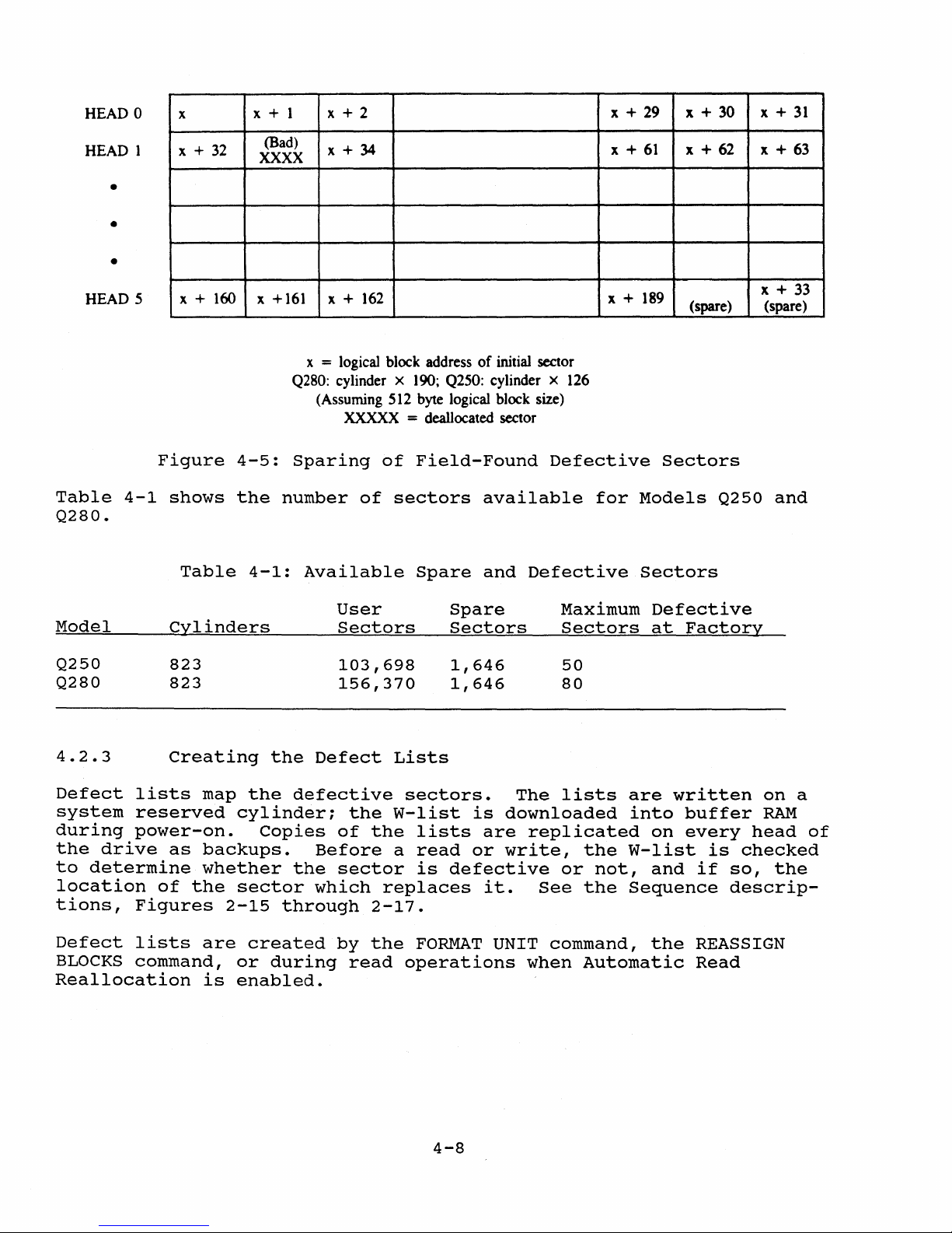
HEAD 0
x
x + 1 x + 2
x + 29 x + 30
x +
31
HEAD 1
HEAD 5
Table
Q280.
•
•
•
4-1
+ 32
x
x + 160
Figure
shows
Table
XXXX
x +161
4-5:
the
4-1:
(Bad)
x
= logical block address
Q280: cylinder
(Assuming 512 byte logical block size)
Sparing
number
Available
x + 34
x + 162
XXXXX
of
of
initial sector
x 190; Q250: cylinder x 126
= deallocated sector
of
Field-Found
sectors
Spare
available
and
Defective
Defective
x +
x + 189
for
x + 62
61
(spare)
Sectors
Models
Sectors
Q250
x + 63
x + 33
(spare)
and
Model
Q250
Q280
4.2.3
Defect
system
during
the
to
determine
lists
reserved
power-on.
drive
location
tions,
Defect
BLOCKS
Figures
lists
command,
Reallocation
Cylinders
823
823
creating
map
as
backups.
whether
of
the
are
is
the
the
cylinder;
Copies
sector
2-15
created
or
during
enabled.
User
Sectors
103,698
156,370
Defect
defective
of
Before
the
sector
which
through
by
the
the
2-17.
the
read
Lists
sectors.
W-list
lists
a
read
is
replaces
FORMAT
operations
Spare
Sectors
1,646
1,646
The
is
downloaded
are
or
write,
defective
it.
UNIT
Maximum
Sectors
50
80
lists
replicated
the
or
not,
See
the
command,
when
Automatic
Defective
at
Factory
are
written
into
on
buffer
every
W-list
and
Sequence
the
on
RAM
head
is
checked
if
so,
the
descrip-
REASSIGN
Read
a
of
4-8
Page 67
There
are
four
different
defect
lists:
P-list.
drive
track
life
G-list.
detected
detected
D-list.
by
the
merged
W-list.
of
is
and
the
user
into
The
tested
The
during
either
The
The
replacements.
from
the
P-list,
operation
4.2.4
At
any
time
o Map
primary
in
can
never
drive.
grown
field
by
defect
to
request
the
G-list.
working
The
of
the
Updating
during
out
of
defects,
defect
the
be
defect
the
data
list:
W-list
G-list,
drive.
the
normal
the
list:
factory.
modified
list:
operation
user,
list:
the
drive
the
is
and
Drive
operation,
defective
and
uses
the
It
is
by
a
the
list
of
the
or
by
the
the
list
to
map
list
of
constructed
D-list.
Using
the
blocks.
the
REASSIGN
list
written
user--it
of
drive.
read
of
them
defective
from
This
Defect
the
user
The
of
defects
on
a
is
preserved
accumulated
The
operation.
defective
out.
sectors
the
defects
list
is
Lists
can
choose
user
can
BLOCKS
found
system
defects
defects
sectors
The
D-list
and
used
during
to:
submit
command.
when
reserved
for
the
are
provided
will
their
combined
aD-list
the
be
o
o
In
any
of
updates
See
the
commands
Rely
SELECT
idefects
Reformat
combinations
without
Factory
Grown
Existing
Provided
Factory
Grown
All
known
the
above
the
G-list.
Q200
and
Series
options
on
the
command.
and
the
defect
defects
defects
defects
defects
and
and
Automatic
The
reallocates
drive
of
with
defect
lists
only
only
only
provided
provided
defects
defects
cases,
The
the
P-list,
Programmers
mentioned.
Read
drive
the
the
lists:
defects
drive
however,
Manual
Reallocation
automatically
sectors.
FORMAT
(use
(use
(use
(use
(use
(use
(use
(use
UNIT
no
P-list
G-list
P-list
D-list
P-list
G-list
P-list,
reconstructs
remains
for
details
option
detects
command,
defect
only)
only)
and
only)
and
and
G-list,
the
untouched.
on
of
lists)
G-list)
D-list)
D-list)
W-list
use
the
drive
using
of
MODE
these
D-list)
and
the
4-9
Page 68

4.3
Grounding,
Electrostatic
Discharges,
and
EMI
The 5 Vdc
metal
plate
holes
casting
wire
shock
is
in
to
(a
heavy
frequencies)
fastened
One
suitable
which
to
Such
accomodates
accept
a
ground
o
o
EMI
may
be
supplies
as
the
Q250/Q280
and
motors,
strong
field:
and
12
Vdc
mount
plastic.
the
shock
cabinet
brackets
Therefore,
mount
ground.
braid
to
from
the
cabinet
base
mating
18
the
grounding
connection
Electrostatic
touching
cause
over
soft
20
the
kilovolts
Electromagnetic
EMI
may
also
due
to
nearby
(especially
drive),
even
up
lamp
to
returns
brackets
is
recommended
ground
casting.
part
AWG
is
wire.
braid.
is
discharges
drive
(random,
Interference
cause
radio
those
heavy
dimmers.
4
volts/meter
are
connected
are
electrically
mounting
does
If
desired,
to
The
a
push-on
The
desirable
after
non-repeating)
may
cause
soft
or
TV
operating
electrical
The
to
ensure
the
male
receptacle,
mating
if:
occur
walking
permanent
errors.
stations,
from
drive
over
the
not
an
male
lug
(for
(EMI)
the
machinery
is
a
range
to
the
isolated,
drives
directly
installer
low
tab-type
is
AMP
part
used
example,
over
a
errors,
damage.
is
present.
chopper-type
same
rated
of
base
casting.
and
by
the
connect
can
impedance
grounding
Faston
AMP
PIN
should
by
carpet).
but
5
volts
such
to
operate
20
Hz
to
the
face-
mounting
the
run
a
ground
to
high
PIN
61761-2.
62187-1,
be
chosen
personnel
These
discharges
Excessive
power
or
12
as
elevators
in
20
MHz.
The
base
lug
may
volts
a
If
EMI
analysis:
operating;
Surge
suppressors
problem
is
suspected
see
try
persists,
if
the
different,
in
contact
and
grounding
problems
the
ac
occur
dedicated
lines
Quantum's
doesn't
only
sources
to
Technical
4-10
other
help,
when
of
equipment
use
the
suspected
5
volts
Support
some
and
may
Group.
common
source
12
volts.
help.
sense
is
If
the
Page 69
SECTION
5.
MAINTENANCE
5.1
5.2
o
o
o
o
o
o
o
Maintenance
Preventive
adjustments,
board.
DO
NOT
open
which
Do
board.
Do
Avoid
down
Do
are
not
lift
not
operate
harsh
carefully.
not
move
Always
removed.
headstack
Level
1
Maintenance
Replacement
Precautions
maintenance
either
the
HDA
also
the
seals.
drive
handle
the
shocks
the
drive
This
time
assembly
of
the
to
or
by
the
drive
to
the
for
is
in
the
entire
is
not
the
HDA
attempt
its
drive
without
drive
30
required
landing
drive.
required.
or
on
to
remove
faceplate
by
its
at
seconds
for
zone.
the
its
shock
any
after
the
There
printed
the
or
printed
shock
mount
time.
power
AIRLOCK
are
labels,
mount
brackets.
Always
has
to
no
circuit
circuit
brackets.
set
been
lock
some
the
of
it
o
o
o
Replacement
Do
not
approval
cause
to
be
Exchange
isolating
Models
require
require
and
Q250
different
a
U18).
Replacement
listed
common
in
hand
of
exchange
from
user
written
of
PCB.
the
problem
and
PCB
equipped
of
SECTION
tools
plug-in
Quantum.
data
over
See
Q280,
EPROMs,
shock
6.
are
EPROM
CAUTION
different
to
be
and
section
to
the
and
drives
and
with
mounts,
Besides
required.
on
printed
EPROMs
The
lost,
destroyed.
5.5
HDA
that
64
Kbytes
brackets,
the
without
wrong
or
for
or
with
EPROM
servo
information
the
and
drives
of
and
replacement
circuit
tracks
PCB.
without
with
RAM
faceplate,
board
may
Note
DisCache
(U16,
parts,
(PCB).
on
that
DisCache
U17,
as
only
5-1
Page 70
NOTE
Users
The
Quantum
Level
drive
5.3
Level
service
5.4
Both
nectors.
ribbon
lOX
magnifier
cable
clean
with
5.5
must
limit
warranty
2
procedure
will
be
billed
Level
2
maintenance
center
o
Level
Connector
intermittent
Before
cable
connector
that
gently
the
a
contact-cleaning
while
contacts
PCB
Waveforms
their
service
is
is
attempted.
at
2
Maintenance
is
performed
or
at
the
1
plus
repair
Maintenance
problems
troubleshooting
on
all
wires
the
drive
by
wiping
null
the
prevailing
factory.
and
the
solvent.
and
Techniques
to
and
of
solid
SCSI
are
is
operating
them
Level
void
All
by
HDA
if
time
trained
and
problems
by
observing
bus:
crimped
with
1
during
the
and
rates.
PCBs.
check
to
and
a
lint-free
the
HDA
is
material
personnel
can
be
waveforms,
visually
the
contacts;
watch
warranty
opened
at
caused
for
cloth
period.
or
any
to
repair
an
authorized
by
inspect
with
a
3X
flex
intermittents;
moistened
the
con-
the
to
the
The
waveforms
shooting:
isolate
If
a
drive
following
most
circuits
to
a
problem
waveform
microprocessor,
loop,
These
write,
waveform
recalibrate.
almost
It
and
5.5.1
is
Sense
o
all
easier
Keys
Special
150
two
and
described
determine
to
successfully
tests
must
operate:
EPROM,
and
SCSI
tests
They
circuits
to
check
reported
Test
MHz
or
a
(or
four
delaying
in
if
the
the
board
recalibrates
are
DICEY, FYLO,
interface.
are
primarily
concentrate
and
require
write
to
Equipment
better)
channels.
sweep
this
PCB
or
not
power,
on
functions
the
host
oscilloscope
is
section
is
the
likely
paR,
seek,
useful
read
the
least
over
High
useful.
may
operating
HDA.
when
operating
to
RAM
servo,
with
functions;
special
by
noting
the
impedance
be
reveal
test,
SCSI
with
observed
correctly,
in
any
motor
read,
a
drive
these
test
the
Sense
bus.
differential
probes
for
trouble-
or
to
a
system,
problems,
control,
phase-Iocked-
that
doesn't
exercise
equipment.
Error
input
are
required,
the
since
Codes
and
5-2
Page 71

o
various
clip-on
connections
for
tiny
100-pin
IC
legs.
o
o
5.5.2
Place
the
shorting
connector.
and
the
Digital
Extension
bench
is
not
Techniques
drive
plug,
if
The
schematics
Be
careful
ground.
and
-BUF
shorted
write
Some
test
of
connector,
shorts.
dc
voltmeter.
cable,
while
connected
required.
and
so
the
PCB
installed.
waveforms
are
in
not
Be
especially
WR
GATE.
to
ground
over
the
and
signals
allowing
Waveform
is
easily
Plug
are
shown
SECTION
CAUTION
to
short
If
or
another
destroy
can
where
the
to
power.
Descriptions
accessible.
in
power,
in
3.
IC
pins
careful
either
data
there
be
and
observed
is
drive
Connection
Figures
together
with
of
these
signal,
servo
less
to
but
2-12,
-WR
signals
the
tracks.
at
danger
be
operated
Remove
not
the
or
GATE
drive
J5,
the
of
to
5-1,
to
the
the
SCSI
5-2
is
may
on
SCSI
WS
bus
and
a
bus
5-3
1.
DC
Measure
5 V
3.7
2.5
3.7
2.
Spin-up
Listen
must
be:
o A
o 1 V
Voltages
(all
dc
and
V
dc
V
dc
V
dc
to
the
continuous
-SPIN
tests
The 2 MHz
FYLO,
+
with
respect
12 V dc
reference
reference
reference
motor
spin
signal
are
passed.
peak-to-peak
is
U9.
input
voltage
voltage
voltage
up.
low
level
after
at
derived
to
power,
In
the
2
ground):
at
pin
at
pin
at
pin
order
on
U8,
RAM
MHz
on
from
the
near
10
11
12
for
test
top
pin
12
J2,
of
of
of
the
and
of
MHz
U28.
U10.
U10.
2.
or
motor
DICEY
other
1 V
clock,
on
J5.
to
asserts
initialization
dc,
on
divided
spin,
U8,
there
this
pin
down
4.
by
5-3
Page 72

3.
RDX,
Use
the
6
and
head,
disk
outer
difficult
RDY,
oscilloscope
7
of
U2.
amplified
diameter,
or
and
-WEDGE
This
by
the
impossible
differential
is
RDX
and
flex
15
mV
to
circuit.
at
sync,
the
input
RDY,
inner
and
and
the
Expect
diameter.
shows
connect
analog
about
a
broad
signal
20
This
band
the
from
mV
probes
a
p-p
signal
on
the
to
read
at
is
screen.
pins
the
Now,
J5.
of
trigger
The
one
wedge,
Note
4.
Use
that
+RAW
another
observe
a
TTL-type
5.
+ENCODED
Observe
of
FYLO,
6.
+READ
Observe
nal,
the
CLOCK,
and
that
servo
another.
trigger
-WEDGE
DATA
oscilloscope
+RAW
pulse
at
pin
and
DATA
this
input
and
its
the
the
oscilloscope
bursts
To
on
requires
DATA,
for
DATA
4
of
is
the
at
the
to
presence
pulse
can
separate
pin
5
the
each
U9,
same
same
DICEY,
detector
now
of
that
channel,
input
transition
or
as
time
ready
means
them
U13,
signal
pin
+RAW
and
on
-WEDGE,
be
observed,
and
the
13
DATA.
as
RDX
to
the
FYLO
and
observe
delay
pulse
and
simultaneously
to
FYLO,
of
RDX
of
J5.
and
be
decoded.
servo
is
are
pin
12
but
all
the
the
sweep.
detector
on
and
+ENCODED
RDY.
It
It
keeping
operating.
of
details
and
pin
RDY.
is
is
U13,
or
wedges
FYLO
with
6
of
U9.
DATA
is
a
TTL-type
synchronous
the
head
pin
are
of
be
RDX
the
on
5
of
on
top
just
one
working.
and
RDY,
Observe
output
sig-
to
track,
RD
7.
AMC
Observe
signal
seconds
pulse
amplitude
amplitude
with
5.5.3
Test
-WEDGE.
Test
connector
provides
shooting.
Circuit
BURST
-WEDGE.
in
duration)
of
Connector
a
convenient
The
PEAK,
the
FYLO
J5
signals
Look
(from
servo
must
is
pin
for
going
the
J5
used
place
1
of
a
series
negative
3.7
bursts,
be
working
Signals
in
are
listed
U10,
the
to
V
dc
and
factory
observe
5-4
or
of
base
the
to
in
pin
pulses
from
group
observe
some
Table
2
a
line)
to
of
J5.
(each
3.7
is
occurs
this.
test
signals
5-1.
Trigger
about
V
dc
base
proportional
simultaneously
the
PCB,
for
using
10
micro-
line.
but
trouble-
to
it
the
The
the
also
Page 73

Pin
Signal
Name
Table
5-1:
Test
Connector
Description
J5
Signals
4
5
6
7
8
9
1
2
3
CAGC
BURST
SET
HYST
DET
REF
-WEDGE
GND
5
Vdc
12
Vdc
12
Vdc
PEAK
AGC
voltage
2.3.5
See
AMC
Figure
1.2
V
factory
margin.
0.2
V
factory
margin.
See
RDX,
5.5.2,
and
Circuit
5-3.
dc.
test
dc.
test
and
for
section
This
This
RDY,
Figure
to
to
and
U2
(B).
2.3.7.
in
section
voltage
check
voltage
check
-WEDGE
5-2.
the
the
See
is
drive's
is
drive's
in
section
5.5.2,
changed
changed
section
and
in
in
10
11
12
13
14
15
16
5
Vdc
GND
N/C
+ENCODED
+DATA
LOCK
N/C
+TEST
RD
DATA
CLOCK
Same
TTL
sync
Same
5-5
as
+RAW
Level.
pattern
as
+RD
DATA.
Asserted
check.
CLOCK.
See
by
See
Figure
DICEY
Figure
5-1.
at
2-13.
end
of
Page 74

Figure
5-1:
Test
Waveforms(l)
TOP:
+RAW
BOTTOM:
DATA
+RD
(1
DATA
Vjdiv.)
(1
Vjdiv.)
5-6
Page 75
Figure
5-2:
Test
Waveforms(2)
TOP:
RDX,
(Differential,
BOTTOM:
RDY
-WEDGE
5
(5
mV/div.)
V/div.)
5-7
Page 76

Figure
5-3:
Test
Waveforms(3)
TOP: -READ
(Differential,
BOTTOM:
BURST
SIG,
+READ
100
PEAK
SIG
mv/div.)
(1
V/div.)
5-8
Page 77

SECTION
6.
PARTS
LISTS
6.1
The
Spare
following
available
this
refer
is
to
Part
Number
20-22007
20-22017
20-22027
20-22008
20-22018
20-22009
Parts
through
a
very
section
List
abbreviated
Quantum's
limited
6.2.
Description
PCB-7
PCB-7
PCB-7
PCB-8
PCB-8
PCB-9
(standard)
(standard
(standard
(standard
(standard
(standard
list.
list
Customer
For
provides
a
complete
with
with
with
with
with
warm-reset
DisCache
warm-reset)
warm-reset
warm-reset
part
Support
numbers
for
Department.
list
of
PCB
rework)
rework)
and
DisCache)
and
green
subassemblies
Note
that
components,
LED)
6-1
Page 78

6.2
Reference
Parts
List(s)
The
tions
following
illustrations)
iterations
ifically,
documented
of
the
here.
parts
the
most
lists
provided
Q200
current
correspond
Series
revisions
in
PCB
to
section
are
of
the
3.
detailed
PCB-7,
PCB
As
layouts
in
section
in
these
PCB-8
and
(Parts
3,
lists.
PCB-9
Loca-
several
Spec-
are
6-2
Page 79

a
Ouantum
Quantum
1804
Milpitas,
Corporation
McCarthy
CA 95035
Blvd.
 Loading...