

Page 1
9732 Parallel Configuration for Increased Current Output
NOTE: If the proper diodes are not implemented (outlined below), damage may occur resulting in a void of
warranty. If in doubt, contact Quantum Composers for additional information.
Scope:
This document overviews the basic theory and operation pertaining to wiring output channels A & B in parallel for
the purpose of increasing output current.
Theory:
The 9732 Series Current Generator allows for the outputs on Channels A & B to be wired together in a parallel
configuration; thus, potentially allowing for current levels up to 12 Amps through the load. This can be
accomplished ONLY with the implementation of 2 external blocking diodes. When operating in this mode, the
limitations on each channel remain constant; although, the current settings will now be additive through the
load. The user may also incorporate a “piece-wise” current waveform by properly altering the pulse widths and
delays.
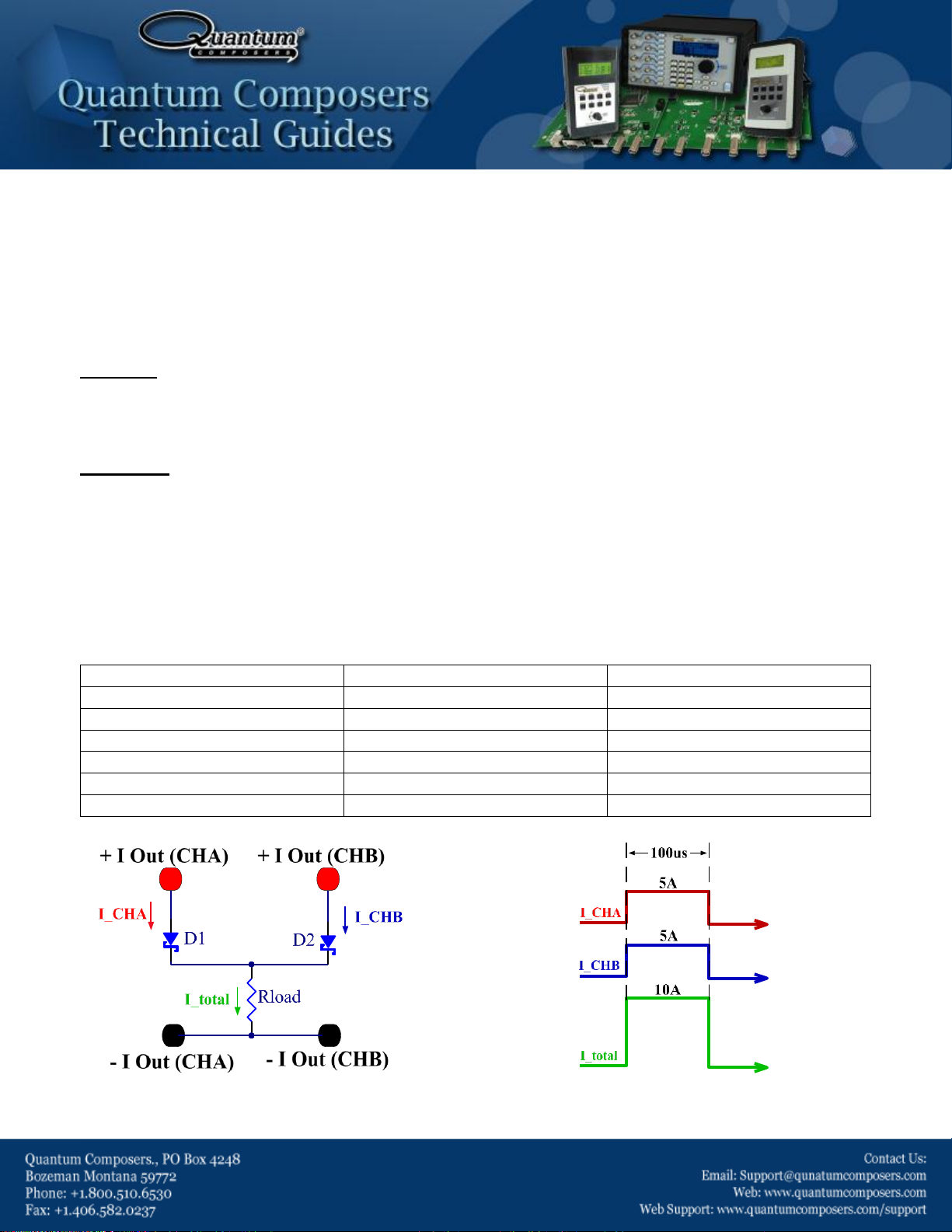
The following example setup represents the potential capabilities of this configuration:
Channel Parameters
Load Parameters
Diode Characteristics
CHA: Amplitude = 5 Amps
Impedance ≤ 3 Ω (includes cabling)
Forward Voltage Drop ≤ 1V
CHA: Width = 0.0001000 s
Reverse Voltage Breakdown ≥ 30V
CHA: Delay = 0 s
DC Current Rating ≥ 30A
CHB: Amplitude = 5 Amps
CHB: Width = 0.0001000 s
CHB: Delay = 0 s
Figure 1- Parallel Schematic Representation Figure 2 – Resulting Current Waveforms
Page 2
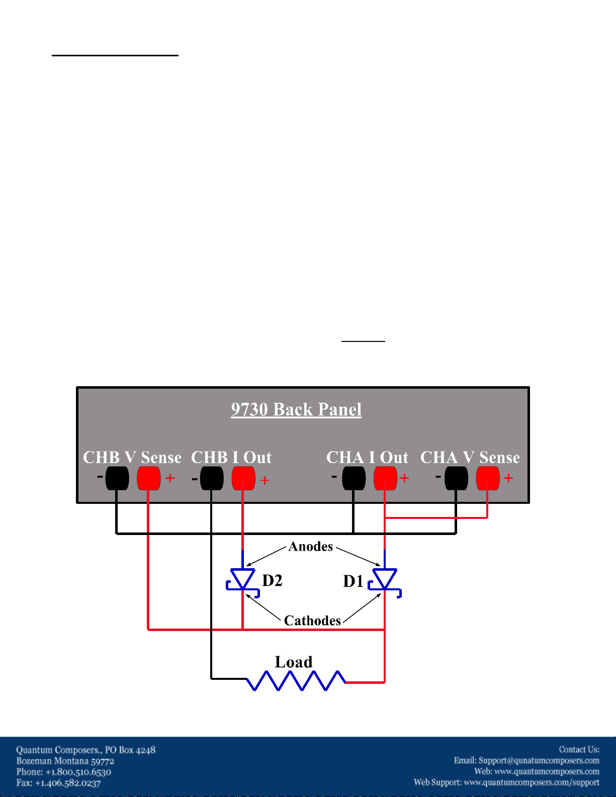
Implementation:
The figure shown below represents the recommended wiring to achieve the parallel configuration. Note that the
blocking diodes are placed immediately at the output on each channel’s positive terminal. To prevent damage to
the 9732, it is EXTREMLY important that the anodes of both diodes be connected to the positive channel
terminals (shown below). Refer to the following list of suggested diodes to use in this configuration:
Suggested Diodes Used at D1 & D2:
-On Semiconductor: MBRB4030T4G
-STMicroelectronics: STPS30M60ST
-Vishay: VT4045BP-M3/4W
Voltage Monitors:
As seen below, the voltage monitors of either channel may be placed before or after the blocking diodes,
depending on what measurements are required. If the voltage prior to the diodes is to be monitored, connect
the positive voltage monitor to the anode of the corresponding blocking diode. If the voltage at the load is to be
monitored, connect the positive voltage monitor as close to the load as possible. Connecting the voltage
monitors as shown below allows one to monitor both the voltage across the load as well as the inherent voltage
drop across the blocking diodes.
Current Monitors:
The current monitors on each channel represent each channel’s individual current. The total current through the
load can simply be measured as the summation of the two current monitor signals.
Figure 3 – Parallel Configuration Wiring
Page 3

Limitations:
Due to internal power supply limitations, the total current may not exceed 12A regardless of the load’s
impedance.
If the channels are wired in parallel, only the current output has the opportunity to increase as the bank voltage
will remain constant (~19V Compliance). In this scenario, the available voltage will be further decreased due to
the inherent voltage drop from the blocking diodes; thus, it is highly recommended that a diode be used with a
small forward voltage rating (see above for suggested diodes).
Example: A total load impedance of 4 Ω is being placed at the output of CHA & CHB in parallel. If blocking
diodes are used with a forward voltage rating of 0.7V, what is the maximum current allow by the unit?
1) The compliance voltage will be approximately:
V = (19V – [2 * 0.7V]) = 17.6V.
2) The maximum allowable current by each individual channel would be:
I ≤ 17.6V/4 Ω I ≤ 4.4 Amps
3) The maximum allowable current by the unit in the parallel configuration:
I ≤ 2*(4.4 Amps) I ≤ 8.8 Amps
Page 4

Operating Results:
The following tests show results upon wiring channels A & B in parallel. It should be noted that on all 3 tests, the
voltage monitor (CH4 in the scope shots) was placed after the blocking diodes and immediately at the load.
Test 1
Channel Parameters
CHA: Amplitude = 2 Amps CHB: Amplitude = 2 Amps
CHA: Width = 0.0005000 s CHB: Width = 0.0005000 s
CHA: Delay = 0 s CHB: Delay = 0 s
Load Parameters
Total Load Impedance = 0.75 Ω (includes cabling)
Diode Characteristics
Forward Voltage Drop ≤ 1V Reverse Voltage Breakdown = 50V DC Current Rating ≥ 30A
CH1: Pearson I Monitor(0.1V/1A) CH2: I Monitor CHA(0.5V/1A) CH3: I Monitor CHB(0.5V/1A) CH4: V Monitor(0.2V/V)
Page 5

Test 2
Channel Parameters
CHA: Amplitude = 5 Amps CHB: Amplitude = 5 Amps
CHA: Width = 0.0005000 s CHB: Width = 0.0005000 s
CHA: Delay = 0 s CHB: Delay = 0 s
Load Parameters
Total Load Impedance = 0.75 Ω (includes cabling)
Diode Characteristics
Forward Voltage Drop ≤ 1V Reverse Voltage Breakdown = 50V DC Current Rating ≥ 30A
CH1: Pearson I Monitor(0.1V/1A) CH2: I Monitor CHA(0.5V/1A) CH3: I Monitor CHB(0.5V/1A) CH4: V Monitor(0.2V/V)
Page 6

Test 3 – Piecewise Waveform
Channel Parameters
CHA: Amplitude = 3 Amps CHB: Amplitude = 5 Amps
CHA: Width = 0.0003000 s CHB: Width = 0.0005000 s
CHA: Delay = 0.0001000 s CHB: Delay = 0 s
Load Parameters
Total Load Impedance = 0.75 Ω (includes cabling)
Diode Characteristics
Forward Voltage Drop ≤ 1V Reverse Voltage Breakdown = 50V DC Current Rating ≥ 30A
CH1: Pearson I Monitor(0.1V/1A) CH2: I Monitor CHA(0.5V/1A) CH3: I Monitor CHB(0.5V/1A) CH4: V Monitor(0.2V/V)
 Loading...