

Page 1
QD14XL0701 Page
1
Prepared by: Date
HC Liu 5/19/2003
Formal
Quanta Display Inc.
SPECIFICATION
Specification for
TFT LCD Module
Model No.
QD14XL07 Rev.02
Doc No. QD14XL07-13
REV.: 13
Issue Date: 6/23/2004
Page: 29 pages
(Cover Page Included)
Customer’s Approval
Date
by By
Approved
Page 2

QD14XL0701 Page
2
These specification sheets are the proprietary product of Quanta Display Inc. (”QDI”) and
include materials protected under copyright of QDI. Do not reproduce or cause any third
party to reproduce them in any form or by any means, electronic or mechanical, for any
purpose, in whole or in part, without the express written permission of QDI.
The device listed in these technical literature sheets was designed and manufactured for
use in OA equipment.
In case of using the device for applications such as control and safety equipment for
transportation (aircraft, trains, automobiles, etc. ), rescue and security equipment and
various safety related equipment which require higher reliability and safety, take into
consideration that appropriate measures such as fail-safe functions and redundant system
design should be taken.
Do not use the device for equipment that requires an extreme level of reliability, such as
aerospace applications, telecommunication equipment (trunk lines), nuclear power control
equipment and medical or other equipment for life support.
QDI assumes no responsibility for any damage resulting from the use of the device which
does not comply with the instructions and the precautions specified in these technical
literature sheets.
Contact and consult with a QDI sales representative for any questions about this device.
Page 3
QD14XL0701 Page
Doc. No. change from QD141X1LH07A to QD141X1LH07A0; Modify
10/23/2001
Page 3 299.5(W)x228.6(H)x5.5typ(D) change to 299.5(W) x228.6(H)x 5.5
D20SFYG (HONDA) Pin
), Checksum
3
Revision History
REV.
0 7/17/2001
1 8/24/2001
2 9/11/2001
3
4 1/23/2002
5 10/04/2002
Date ECN NO. Change Content
N/A Preliminary specification Initiate
N/A Rise/Fall time update, 5 points average 150 nits
N/A
N/A
N/A Update outline drawing
interface cable pin assignments
(D) 5.5 max
Page 6 WR-L16S-VF-1 (JAE) change to LVC17~20 definition
Product ID Change QD141X1LH07 to QD14XL0701 Page 9
VIN=9V,VBB=5V:min 485 VIN=9V,VBB=5V:min 200 Max 300 Page
11 Brightness Control: eliminated block diagram and AC
Electrical characteristic Page15 Modified EDID data structure
Page 19 Optical Data:Wx=0.315±0.02 Wy=0.330
N/A
0.02 Ry=0.327±0.02 Bx=0.148±0.02 By=0.128±0.02
±0.02 Rx=0.595±
Luminance of
white:min 150 Typ:200 Color Gamunt:50% 5dW:1.25 13dW:1.53
Page23
≦
test:1.5G 30min/each axis 1.6G random
6 01/09/2003
7 01/20/2003
8 5/13/2003
9 5/23/2003
10 7/2/2003 N/A Update the LCD curent consumption spec.
11 11/21/2003
12 1/13/2004
13 6/23/2004
N/A Update EDID data for customer request.
N/A Update Data – Mass: 440g.
N/A Update EDID Code according to customer new spec.
N/A Add PPID “C1787” into EDID data and errors correction.
N/A Update PPID from C1787 to C4011 (EDID changed).
EDID Data Correction (Byte 17, “13” Replaced by “D”
N/A
Unchanged.
N/A EDID Update for Adding Ambit Inverter
Temperature cycle— Non Operating: -25? to +65?, Ramp
24?/min, Duration at Temp.=60min, Test cycles=50 Vibration
Page 4
QD14XL0701 Page
1. Application
This specification applies to a color TFT-LCD module, QD14XL07.
2. Overview
This module is a color active matrix LCD module incorporating amorphous silicon TFT
(Thin Film Transistor). It is composed of a color TFT-LCD panel, driver ICs, control circuit
and power supply circuit and a backlight unit. Graphics and texts can be displayed on a
1024×3×768 dots panel with 262,144 colors by using LVDS (Low Voltage Differential
Signaling) to interface and supplying +3.3V DC supply voltage for TFT-LCD panel driving
and supply voltage for backlight.
The TFT-LCD panel used for this module has very high aperture ratio. A low-reflection and
higher-color-saturation type color filter is also used for this panel. Therefore, highbrightness and high-contrast image, which is suitable for the multimedia use, can be
obtained by using this module.
4
Optimum viewing direction is 6 o'clock.
[Features]
1) High aperture panel; high-brightness or low power consumption.
2) Brilliant and high contrast image.
3) Small footprint and thin shape.
4) Light weight.
5) 100% SPWG, style B
3. Mechanical Specifications
Parameter Specifications Unit
Display size 36 (14.1") Diagonal cm
Active area 285.7 (H)×214.3 (V) mm
Pixel format 1024 (H)×768 (V) Pixel
(1 pixel = R+G+B dots)
Pixel pitch 0.279 (H) × 0.279 (V) mm
Pixel configuration R,G,B vertical stripe
Display mode Normally white
Unit outline dimensions (typ.)*1 299(W)×228 (H)×5.2(D)
mm
5.5 Max
Mass (without inverter) Max: 440 g
Surface treatment Anti-glare and hard-coating 3H
Low reflection (~5%)
*1.Note: excluding backlight cables. Outline dimensions are shown in this specification.
Page 5
QD14XL0701 Page
4. Input Terminals
4-1. TFT-LCD panel driving
CN1 (1 channel, LVDS signals – NSC/Ti standard and +3.3V DC power supply)
Using connector: FI-XB30Sx-HFxx/FI-X30Sx-HFxx/equivalent (JAE)
Corresponding connector: TBD
Interface Cable Pin Assignments
PIN NO . SYMBOL FUNCTION
1 VSS Ground
2 VDD Power Supply, 3.3 V (typical)
3 VDD Power Supply, 3.3 V (typical)
4 V EEDID DDC 3.3V power
5 NC Reserved for supplier test point
6 Clk EEDID DDC Clock
7 DATA EEDID DDC Data
8 Rin0- - LVDS differential data input (R0-R5, G0) (odd pixels)
5
9 Rin0+ + LVDS differential data input (R0-R5, G0) (odd pixels)
10 VSS Ground
11 Odd_Rin1- - LVDS differential data input (G1-G5, B0-B1) (odd pixels)
12 Rin1+ + LVDS differential data input (G1-G5, B0-B1) (odd pixels)
13 VSS Ground
14 Rin2- - LVDS differential data input (B2-B5, HS, VS, DE) (odd pixels)
15 Rin2+ + LVDS differential data input (B2-B5, HS, VS, DE) (odd pixels)
16 VSS Ground
17 ClkIN- - LVDS differential clock input (odd pixels)
18 ClkIN+ + LVDS differential clock input (odd pixels)
19 VSS Ground
20 NC No connect
21 NC No connect
22 NC No connect
23 NC No connect
24 NC No connect
25 NC No connect
26 NC No connect
27 NC No connect
28 NC No connect
29 NC No connect
30 NC No connect
Note 1?Relation between LVDS signals and actual data shows below section (4-2).
?
?Note 2?The shielding case is connected with signal GND.
Page 6
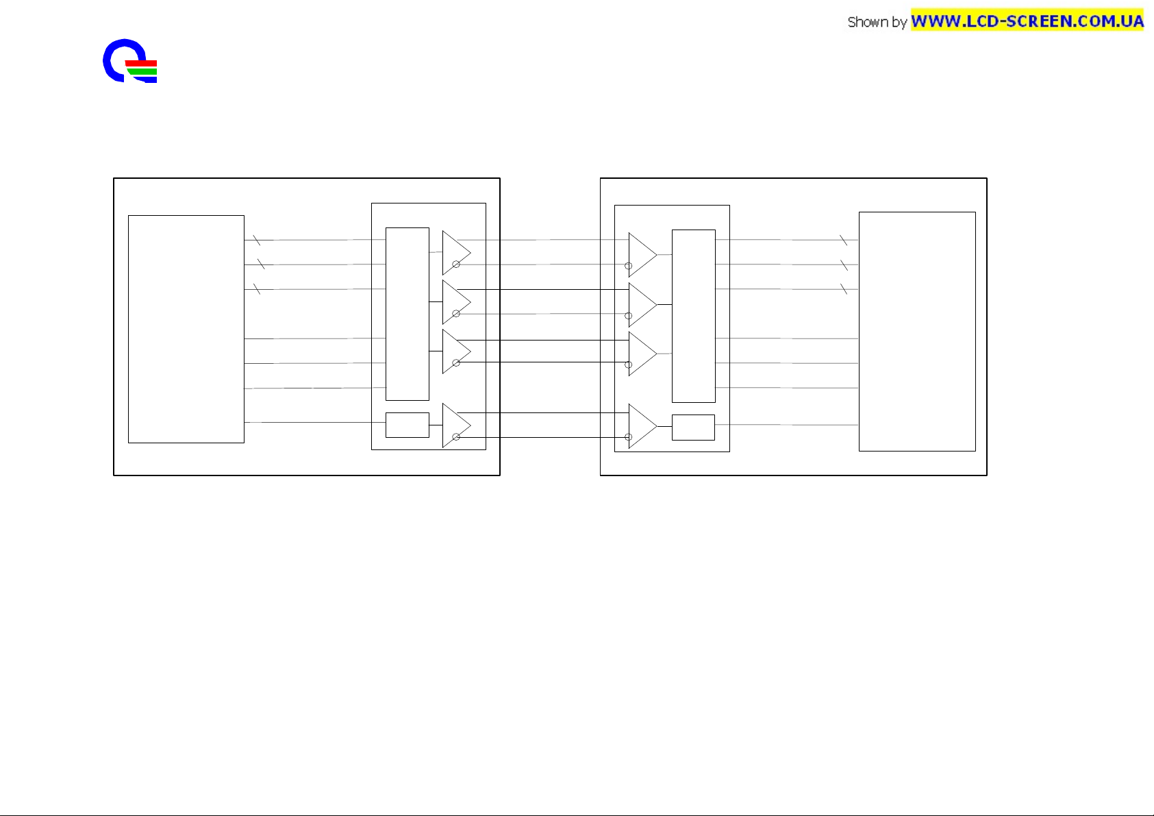
4-2 Interface block diagram
TxIN18
TxIN19
TxIN20
Controller
DS90C*363
DS90CF364
R0~R5 B0~B5
ENAB
Internal circuits
CK
CLK
TxCLK IN
QD14XL0701 Page
6
Using receiver:DS90CF364(National semiconductor) Corresponding Transmitter:DS90C363,DS90C383(National semiconductor
( Computer side)
(TFT-LCD side)
)
R0~ R5
G0~ G5
B0~ B5
Hsync
Vsync
ENAB
TxIN 0~ 5
6
6
TxIN 6~ 11
6
TxIN12~ 17
PLL
TTL PARALLEL-TO-LVDS
RXIN0+(6)
RXIN0-(5)
RXIN1+(9)
RXIN1-(8)
RXIN2+(12)
RXIN2-(11)
RXCLKIN+(1
RXCLKIN-
PLL
RxOUT0~ 5
RxOUT6~ 11
RxOUT12~ 17
RxOUT18
RxOUT19
LVDS-TO-PARALLEL TTL
RxOUT20
RxCLK OUT
6
6
G0~ G5
6
Hsync
Vsync
Page 7
4-3. Backlight driving
amp
Power supply for lamp
CN2: BHSR-02VS-1(JST)
Mating connector: SM02B-BHSS-1-TB (JST) or 87210-0200
QD14XL0701 Page
7
Pin No. Symbol
1
V
HIGH
Power supply for l
Function
(High voltage side)
2
V
LOW
(Low voltage side)
4-4. Inverter driving
Connector pin assignment:
CN3:(Inverter signals and Inverter Power Supply)
Using connector:LVC-D20SYFG(HONDA)
Corresponding connector: LVC-D20LVM-SG (HONDA)
Pin no. Symbol Function
1,2,3 INV SRC Input voltage
4 N.C No connect
5,8,11,13
GND Ground
6 5VSUS System +5V voltage(Inverter no use)
7 5VALW Dallas IC VCC Voltage
9 SDA Brightness control data signal(SMBUS DATA)
10 SCL Brightness control clock signal(SMBUS CLOCK)
12 FPVEE MPS IC Enable voltage
14 N.C. No connect
15 N.C. No connect
16 N.C. No connect
17 N.C. No connect
18 N.C. No connect
19 N.C. No connect
20 N.C. No connect
Page 8
Inverter power supply
Base of Brightness
5. Absolute Maximum Ratings
5-1 LCD module
QD14XL0701 Page
8
Parameter Symbol Condition
Input voltage
+3.3V supply voltage Vcc Ta=25
Storage temperature Tstg
Operating temperature (Ambient) Topa
VI
Ta=25
-
-
? ?
Ratings Unit Remark
0.3 ~ Vcc+0.3
0 ~ + 4
-25 ~ +60
0 ~ +50
V
V
?
?
[Note1]
[Note2]
[Note1] LVDS signals
[Note2] Humidity:95%RH Max. at Ta?40?.
Maximum wet-bulb temperature at 39? or less at Ta>40?.
No condensation.
5-2. Inverter driving
5-2.1. Backlight lifetime
The backlight system is an edge-lighting type with single CCFT (Cold Cathode
Fluorescent Tube).
The lifetime of the lamp are shown in the following table.
Parameter Symbol
Min. Typ. Max. Unit Remark
Lamp life time LL 10000 - - Hour [Note]
[Note] Lamp life time is defined as the time when ? occurs in the continuous
operation under the condition of Ta = 25℃ and SDA data=00HEX
? Brightness becomes 50% of the original value under standard condition.
5.2.2 Recommended Operation Condition
Parameter Symbol Min. Typ Max Unit
Vin 9 - 21 V
voltage
VBB 4.85 5.0 5.2 V
control voltage
Brightness control IC
VBC 4.5 5.0 5.5 V
supply voltage
Logic signals SDA, SCL
0 5 V
FPVEE
Page 9
QD14XL0701 Page
t1
0V
Off
5.2.3 DC Electrical Conditions Ta=25℃
9
Parameter Symbol
Condition Min. Typ Max Unit Remark
IVin VIN=9V,VBB=5V 485
VIN=21V,VBB=5V
Brightness control IC
IVbc VBC=4.5~5.5V - - 200 uA
supply current
Input voltage
Vil VBC=4.5~5.5V - -
SDA
SCL
low
Input voltage
Vih VBC=4.5~5.5V
High
Input voltage
FPVE
E
low
Vil
Input voltage
Vih
VIN=9~21V
VIN=9~21V
High
Note: Brightness control from minmum to maximum
5.2.4. Power ON/OFF sequence
9V≦Vin<21V
10ms≦td
- 585 VIN supply current
200
-
0.7×
- - V
VBC
0 - 0.6
3.0
- 5.0 V
Vin
FPVEE
300
0.3×
VBC
mA Note
V
V
8.0V
td
5.2.5 FPVEE ON sequence
Backlight power on/off is possible with FPVEE.
Make sure to have more than 50-millisecond interval between each power-on.
50ms≦t1
t2≦20ms
3.0V
FPVEE
On
0.6V
t2
5.2.6 The Condition of Shut Down
Please refer to the figure below for the conditions that will cause the inverter shut down.
If the Vin voltage is higher than 8.0V but there is no enable signal, then the inverter will
shut down.
Page 10

QD14XL0701 Page
0V OFF
Current
No Output
Vin shut down voltage 8V
If the Vin voltage is down less than 8.0V, it will cause the inverter shut down.
The enable signal has to be reset to get the inverter started again.
8.0V
Vin
ON
FPVEE
3.0V
0.6V
Output
5.2.7. Brightness Control
SDA data Brightness Notes
10
00HEX Maximum Brightness Set on power-up
01~FEHEX
FFHEX Minimum Brightness
?
Page 11

QD14XL0701 Page
Permissive input ripple
Rise time
t2 t3 t4 t5 t6
6. Electrical Characteristics
6-1.TFT-LCD panel driving Ta=25?
Parameter Symbol Min. Typ. Max. Unit Remark
Vcc Supply voltage Vcc +3.0 +3.3 +3.6
Current dissipation Icc
VRP
-
-
360 560
100 mV p-p Vcc=+3.3V
-
V
mA
[Note2]
[Note3]
voltage
Differential input High
Threshold voltage Low
Input current (High)
Input current (Low)
Terminal resistor
VTH
VTL
IOH
IOL
RT
-
–100
-
-
-
-
-
-
±
+100
-
10
mV VCM=+1.2V
mV
A
µ
[Note1]
VI=2.4V
Vcc=3.6V
-
±
10
µ
A
VI=0V
Vcc=3.6V
100
-
Differential
O
input
Rush current I
1.5 A
RUSH
470uS
11
[Note1] VCM : Common mode voltage of LVDS driver.
[Note2]
On-off conditions for supply voltage
0<t1?10 ms
0<t2?50 ms
0<t3?50 ms
400 ms?t4 ; 200 ms?t5 ; 200 ms?t6
90%
90%
VDD
10%
DATA
t1
10% 10%
CCFL
Page 12

QD14XL0701 Page
12
Vcc
Vcc-dip conditions
1) 2.5 V?Vcc<3.0 V
td?10 ms
td
0 V
.
3
5 V
.
2
2) Vcc<2.5 V
Vcc-dip conditions should also follow the On-off conditions for supply voltage
[Note3]
1. The maximum current pattern: one pixel line at gray-level 8 and fully black pixel line
aside (one line on-off)
2. Typical current pattern: 16-gray-bar pattern, Vcc=+3.3V
R G B
G S 4
R G B
G S 8
. .. .
R G B
G S 0
R G B
G S 5 6
R G B
G S 6 0
Page 13

QD14XL0701 Page
Lamp power
pin is V
LOW
6-2. Backlight driving
The backlight system is an edge-lighting type with single CCFT (Cold Cathode
Fluorescent Tube).
The characteristics of the lamp are shown in the following table.
Parameter Symbol Min. Typ. Max. Unit
Lamp current range IL 5.8 6.1 6.4 mArms [Note1]
Lamp voltage V L 675 Vrms
PL
consumption
Lamp frequency FL 30 60 70 kHz [Note3]
Kick-off voltage Vs
Lamp life time LL 10000
-
-
-
2.7
-
-
-
W
[Note2]
-
1670 Vrms Ta=25
1355 Vrms Ta=0
hour [Note5]
-
Remark
?
[Note4]
?
13
1
Module
Inverter
2
A
~
* 2
[Note1] Lamp current is measured with current meter for high frequency as shown below.
[Note2] Calculated Value for reference ( I
[Note3] Lamp frequency may produce interference with horizontal synchronous frequency,
and this may cause beat on the display. Therefore lamp frequency shall be
detached as much as possible from the horizontal synchronous frequency and
from the harmonics of horizontal synchronous to avoid interference.
[Note4] The voltage above this value should be applied to the lamp for more than 1 second
to start-up. Otherwise the lamp may not be turned on.
L × V L)
[Note5] Lamp life time is defined as the time when either ? or ? occurs in the
? Brightness becomes 50 % of the original value under standard condition.
? Kick-off voltage at Ta = 0? exceeds maximum value.
Note) The performance of the backlight, for example life time or brightness, is much
influenced by the characteristics of the DC-AC inverter for the lamp. When you design or
order the inverter, please make sure that a poor lighting caused by the mismatch of the
backlight and the inverter (miss-lighting, flicker, etc.) never occur. When you confirm it, the
module should be operated in the same condition as it is installed in your instrument.
continuous operation under the condition of Ta = 25? and IL = 6.0 mArms.
Page 14

C
7. Timing characteristics of LCD module input signals
ENAB
B A D E F
7-1. Timing characteristics
(This is specified at digital outputs of LVDS driver.)
Data
Sync
( Vertical)
Item( symbol)
Vsync cycle (TVA)
Min. Typ. Max. Unit Remark
-
16.667
-
ms Negative
803 806 line
Blanking period(TVB) 35 38
Sync pulse width (TVC) 4 6
-
-
line
line
Back porch (TVD) 0 29 line
Sync pulse width + Back porch
35 35 35 line
(TVC+TVD)
Active display area (TVE) 768 768 768 line
Front porch (TVF) 0 3
-
line
QD14XL0701 Page
14
(Horizontal)
Item( symbol)
Hsync cycle (THA) 19.2 20.677
1260 1344 1408 clock
Blanking period (THB) 236 320
Sync pulse width (THC) 8 136
Back porch (THD) 0 160 312 clock
Sync pulse width + Back
porch (THC +THD)
Active display area (THE)
Front porch (THF) 8 24
Min. Typ. Max. Unit Remark
1500 - T
HA
- µ s
-
-
296 THA -
clock
clock
clock
Negative
1024
1024 1024 1024 clock
-
clock
( Clock)
Item Min. Typ. Max. Unit Remark
Frequency
-
65.0 65.0 MHz [Note]
Note) In case of lower frequency, the deterioration of display quality, flicker etc., may be
occurred.
Page 15

(Hsync-Vsync Phase difference)
Vsync
Hsync
ENAB
Hsync
QD14XL0701 Page
15
Item(symbol) Min. Typ.
Hsync-Vsync Phase difference
(THV)
(Hsync-ENAB Phase difference)
THN
Item Min. Typ. Max. Unit Remark
(THN)
7-2 Display position
Item Standards Beginning Ending Unit Remark
THV
0
1
Max. Unit Remark
- THA- T
-
312 clock
HC
clock
Horizontal rising edge of ENAB
rising edge of Hsync
Vertical rising edge of Vsync
0 1024 clock
296 1320 clock [Note1]
35 803 clock
[Note1] ENAB signal must be fixed to low.
Note]
[
(Horizontal display direction)
When ENAB is fixed low, 296 clock are counted from Hsync negative edge and data from
after are available. If you need other timing, please use ENAB signal.
(Vertical display direction)
35 lines are counted from Vsync negative edge and data from next line are available.
(Note of ENAB signal)
ENAB could not be used for the purpose of the vertical display start timing.
Caution
Image will not be displayed on the right position otherwise.
Page 16

7-3. Input Data Signals and Display Position on the screen
Display position of input data
(H,V)
QD14XL0701 Page
UP
16
D1,DH1
D1,DH2
D1,DH3
D1,DH768
D2,DH1 D3,DH1
D2,DH2
R
G
D1024,DH1
B
D1024,
DH768
Page 17

8. Input Signals, Basic Display Colors and Gray Scale of Each Color
QD14XL0701 Page
17
Colors &
Gray scale Gray
Black
Blue
Basic Color Gray Scale of Red Gray Scale of Green Gray Scale of Blue
Green
Cyan
Red
Magenta
Yellow
White
Scale
-
-
-
-
-
-
-
-
R0 R1 R2 R3 R4 R5 G0 G1 G2 G3 G4 G5 B0 B1 B2 B3 B4 B5
0 0 0 0 0 0 0 0 0 0 0 0 0 0 0 0 0 0
0 0 0 0 0 0 0 0 0 0 0 0 1 1 1 1 1 1
0 0 0 0 0 0 1 1 1 1 1 1 0 0 0 0 0 0
0 0 0 0 0 0 1 1 1 1 1 1 1 1 1 1 1 1
1 1 1 1 1 1 0 0 0 0 0 0 0 0 0 0 0 0
1 1 1 1 1 1 0 0 0 0 0 0 1 1 1 1 1 1
1 1 1 1 1 1 1 1 1 1 1 1 0 0 0 0 0 0
1 1 1 1 1 1 1 1 1 1 1 1 1 1 1 1 1 1
Data signal
Black GS0 0 0 0 0 0 0 0 0 0 0 0 0 0 0 0 0 0 0
?
GS1 1 0 0 0 0 0 0 0 0 0 0 0 0 0 0 0 0 0
Darker GS2 0 1 0 0 0 0 0 0 0 0 0 0 0 0 0 0 0 0
?
?
?
?
?
?
?
?
?
?
Brighter GS61 1 0 1 1 1 1 0 0 0 0 0 0 0 0 0 0 0 0
?
GS62 0 1 1 1 1 1 0 0 0 0 0 0 0 0 0 0 0 0
Red GS63 1 1 1 1 1 1 0 0 0 0 0 0 0 0 0 0 0 0
Black GS0 0 0 0 0 0 0 0 0 0 0 0 0 0 0 0 0 0 0
?
GS1 0 0 0 0 0 0 1 0 0 0 0 0 0 0 0 0 0 0
Darker GS2 0 0 0 0 0 0 0 1 0 0 0 0 0 0 0 0 0 0
?
?
?
?
?
?
?
?
?
?
Brighter GS61 0 0 0 0 0 0 1 0 1 1 1 1 0 0 0 0 0 0
?
GS62 0 0 0 0 0 0 0 1 1 1 1 1 0 0 0 0 0 0
Green GS63 0 0 0 0 0 0 1 1 1 1 1 1 0 0 0 0 0 0
Black GS0 0 0 0 0 0 0 0 0 0 0 0 0 0 0 0 0 0 0
?
GS1 0 0 0 0 0 0 0 0 0 0 0 0 1 0 0 0 0 0
Darker GS2 0 0 0 0 0 0 0 0 0 0 0 0 0 1 0 0 0 0
?
?
?
?
?
?
?
?
?
?
Brighter GS61 0 0 0 0 0 0 0 0 0 0 0 0 1 0 1 1 1 1
?
GS62 0 0 0 0 0 0 0 0 0 0 0 0 0 1 1 1 1 1
Blue GS63 0 0 0 0 0 0 0 0 0 0 0 0 1 1 1 1 1 1
0 : Low level voltage, 1 : High level voltage
Each basic color can be displayed in 64 gray scales from 6 bit data signals. According to the
combination of total 18 bit data signals, the 262,144-color display can be achieved on the screen.
Page 18

QD14XL0701 Page
ex:
timing
Established timings 3 (Manufacture’s reserved
18
9.EDID data structure
This is the EDID (Extended Display Identification Data) data format to support displays as
defined in the VESA Plug & Display.
Byte
(decimal)
0 00 Header 00 00000000
1 01 Header FF 11111111
2 02 Header FF 11111111
3 03 Header FF 11111111
4 04 Header FF 11111111
5 05 Header FF 11111111
6 06 Header FF 11111111
7 07 Header 00 00000000
8 08 EISA manufacture code=QDS 44 01000100
9 09 EISA manufacture code (Compressed ASCII) 93 10010011
10 0A Product code: 0005 (P08A) 05 00000101
11 0B Product code (hex, LSB first) 00 00000000
12 0C LCD module Serial No (fixed ”0”) 00 00000000
13 0D LCD module Serial No (fixed ”0”) 00 00000000
14 0E LCD module Serial No (fixed ”0”) 00 00000000
15 0F LCD module Serial No (fixed ”0”) 00 00000000
16 10 Week of manufacture 00 00000000
17 11
18 12 EDID structure version # = 1 01 00000001
19 13 EDID revision # = 3 03 00000011
20 14 Video I/P definition = Digital I/P 80 10000000
21 15
22 16 Max V image size (cm) = 21cm 15 00010101
23 17
24 18
25 19 Red/Green Low bit 8C 10001100
26 1A Blue/White Low bit E9 11101001
27 1B Red X (Rx)(written value “0.588”) 96 10010110
28 1C Red Y (Ry)(written value “0.325”) 53 01010011
29 1D Green X (Gx)(written value “0.308”) 4E 01001110
30 1E Green Y (Gy)(written value “0.563”) 90 10010000
31 1F Blue X (Bx)(written value “0.148”) 25 00100101
32 20 Blue Y (By)(written value “0.116”) 1D 00011101
33 21 White X (Wx)(written value “0.315”) 50 01010000
34 22 White Y (Wy)(written value “0.330”) 54 01010100
35 23 Established timings 1 00 00000000
36 24 Established timings 2 00 00000000
Byte
(hex)
Field Name and Comments Value
Year of manufacture – 1990 (ex2000-1990=10),
2003-1990=13=D (hex)
Max H image size (cm) = 29cm
Display gamma ( 2.2× 100 ) –100= 120
Feature support (no DMPS, Active off, RGB,
BLK1)
Value
(hex)
0D 00001101
1D 00011101
78 01111000
0A 00001010
(binary)
37 25
38 26 Standard timing ID1 01 00000001
39 27 Standard timing ID1 01 00000001
40 28 Standard timing ID2 01 00000001
41 29 Standard timing ID2 01 00000001
42 2A Standard timing ID3 01 00000001
43 2B Standard timing ID3 01 00000001
44 2C Standard timing ID4 01 00000001
45 2D Standard timing ID4 01 00000001
46 2E Standard timing ID5 01 00000001
timing)
00 00000000
Page 19

QD14XL0701 Page
#1 Horizontal sync offset/width/Vertical sync
interlaced, Normal, no stereo, Separate sync,
(pixelclks),value =192
Module “A” Revision = Example: 00, 01, 02,
47 2F Standard timing ID5 01 00000001
48 30 Standard timing ID6 01 00000001
49 31 Standard timing ID6 01 00000001
50 32 Standard timing ID7 01 00000001
51 33 Standard timing ID7 01 00000001
52 34 Standard timing ID8 01 00000001
53 35 Standard timing ID8 01 00000001
54 36 Detailed timing descriptor#1 64 01100100
55 37 #1 fck 19 00011001
56 38 #1 Horizontal active 1024=400h “00” 00 00000000
57 39 #1 Horizontal blanking 320=140h “40” 40 01000000
58 3A #1 Horizontal active/Horizontal blanking “41h” 41 01000001
59 3B #1 Vertical active 768=300h “00” 00 00000000
60 3C #1 Vertical blanking 38=026h “26” 26 00100110
61 3D #1 Vertical active/Vertical blanking “30h” 30 00110000
62 3E #1 Horizontal sync, offset 24=018h “18” 18 00011000
63 3F #1 Horizontal sync, width 136=088h “88” 88 10001000
64 40 #1 Vertical sync, offset/Vertical sync, width 36 00110110
19
65 41
offset/width
00 00000000
66 42 #1 Horizontal image size 290mm=122h “22” 1D 00011101
67 43 #1 Vertical image size 220mm=0DCh “DC”
D6
11010110
68 44 #1 Horizontal image size / Vertical image size 10 00010000
69 45 Horizontal border 00 00000000
70 46 Vertical border 00 00000000
71 47
NonH/V pol Negatives
18 00011000
72 48 Flag 00 00000000
73 49 Flag 00 00000000
74 4A Reserved 00 00000000
75 4B Dummy Descriptor 0F 00001111
76 4C Flag 00 00000000
77 4D Value = HSPW
78 4E Value = HSPW
79 4F Value = Thbp
80 50 Value = Thbp
81 51 Value = VSPW
82 52 Value = VSPW
83 53 Value = Tvbp
84 54 Value = Tvbp
85 55 Thp
86 56 Thp
87 57 Tvp
88 58 Tvp
89 59
= value*2 + HA
min
= value*2 + HA
max
= value*2 + VA
min
= value*2 + VA
max
03, etc.
/2 (pixel clks) =8/2 =4 04 00000100
min
/2 (pixel clks) =384/2 = 192 C0 11000000
max
/2 (pixel clks) =92/2 =46 2E 00101110
min
/2 (pixel clks) =384/2 =192 C0 11000000
max
/2 (line pulses)= 4/2 =2 02 00000010
min
/2 (line pulses)= 35/2 =17 11 00010001
max
/2 (line pulses)= 35/2 =17 11 00010001
min
/2 (line pulses)= 35/2 =17 11 00010001
max
pixel clks
pixel clk
lines
lines
(pixel clks),value= 118
(line pulses),value =18
(line pulses),value =99 63 01100011
76 01110110
C0 11000000
12
00010010
00 00000000
90 5A Flag 00 00000000
91 5B Flag 00 00000000
92 5C Reserved 00 00000000
93 5D
Dummy Descriptor
FE 11111110
94 5E Flag 00 00000000
95 5F Dell PN Character C 43 01000011
96 60 Dell PN Character 4 34 00110100
97 61 Dell PN Character 0 30 00110000
98 62 Dell PN Character 1 31 00110001
99 63 Dell PN Character 1 31 00110001
100 64 LCD Supplier EEDID Reversion # 02 02 00000010
Page 20

QD14XL0701 Page
(If<13 char, then terminate with ASCII code 0Ah, set
(If<13 char, then terminate with ASCII code 0Ah, set
(If<13 char, then terminate with ASCII code 0Ah, set
101 65 Manufacturer PN 00 00000000
102 66 Manufacturer PN 00 00000000
103 67 Manufacturer PN 00 00000000
104 68 Manufacturer PN 00 00000000
105 69 Manufacturer PN 00 00000000
106 6A Manufacturer PN 00 00000000
107 6B Manufacturer PN 00 00000000
108 6C Flag 00 00000000
109 6D
110 6E Flag 00 00000000
111 6F Data Type Tag FE 11111110
112 70 Flag 00 00000000
113 71 SMBUS Value = 20 nts D8 11011000
114 72 SMBUS Value = 30 nts C8 11001000
115 73 SMBUS Value = 40 nts B8 10111000
116 74 SMBUS Value = 50 nts A8 10101000
117 75 SMBUS Value = 70 nts 90 10010000
118 76
119 77 SMBUS Value = 135 nts 50 01010000
120 78 SMBUS Value = Max nts 00 00000000
121 79 Number of LVDS receiver chips 01 00000001
122 7A Panel type-Standard 00 00000000
Flag
SMBUS Value = 100 nts
00 00000000
70 01110000
20
123 7B
124 7C
125 7D
126 7E Extension flag 00 00000000
127 7F Checksum 2B 00101011
remaining char=20h)
remaining char=20h)
remaining char=20h)
0A 00001010
20 00100000
20 00100000
Page 21

QD14XL0701 Page
10. Optical Characteristics
Ta=25?, Vcc=+3.3V
21
Parameter Symbol Condition Min. Typ. Max. Unit
Viewing
Angle
Range
Contrast ratio
Response
Time
Horizontal
Vertical
?
CR
Rise
Decay
21,?22 CR>10 40
?
11 10
?
12 30
n
r
t
d
t
?=0°
?=0°
300
-
-
-
-
-
-
12.5
22.5
-
-
-
-
-
-
Chromaticity of Wx 0.295 0.315 0.335
White Wy 0.310 0.330 0.350
Chromaticity of
Red
Chromaticity of
Green
Chromaticity of
Blue
Luminance of white
Rx
Gx
Gy
Bx
Y
Ry
By
L2
0.558
0.295
0.278
0.533
0.118
0.086
Center 150 200
0.588
0.325
0.308
0.563
0.148
0.116
0.618
0.355
0.338
0.593
0.178
0.146
-
Deg.
Deg.
Deg.
ms
ms
Cd/m
Remark
[Note1,4]
[Note2,4]
[Note3,4]
[Note4]
2
IL =
6.0mArms
Note4?
?
Color Gamut
White Uniformity
White Uniformity
The measurement shall be executed 30 minutes after lighting at rating.
?
?
d
W
d
W
50% NTSC
13 Points
5 Points
-
-
-
-
1.53
1.25
FL=60kHz
[Note5]
[Note5]
(typical condition : IL = 6.0 mArms)
The optical characteristics shall be measured in a dark room or equivalent state with the
method shown in Fig.3.
Page 22

Photodetector (BM-5A:TOPCON)
Field=2°
QD14XL0701 Page
400mm
22
TFT-LCD module
LCD panel
Center of the screen
Fig.3 Optical characteristics measurement method
Page 23

[Note1] Definitions of viewing angle range:
768
512
10mm
10mm
10mm
10mm
256
B C D E
192
384
576
G H I J K L M
[Note2] Definition of contrast ratio:
The contrast ratio is defined as the following.
QD14XL0701 Page
23
Luminance (brightness) with all pixels white
Contrast Ratio (CR)=
Luminance (brightness) with all pixels black
[Note3] Definition of response time:
The response time is defined as the following figure and shall be measured by
switching the input signal for "black" and "white".
[Note4] This shall be measured at center of the screen.
[Note5] Definition of white uniformity:
Maximun Luminance of 5/13 points
dw =
Minimum Luminance of 5/13 points
(5 Points A,B,C,D,E 13 Points A,B,C,D,E,F,G,H,I,J,K,L,M)
F
A
Page 24

QD14XL0701 Page
24
11. Display Quality
The display quality of the color TFT-LCD module shall be in compliance with the Incoming
Inspection Standard.
12.Handling Precautions
a) Be sure to turn off the power supply when inserting or disconnecting the cable.
b) Be sure to design the cabinet so that the module can be installed without any extra
stress such as warp or twist.
c) Since the front polarizer is easily damaged, pay attention not to scratch it.
d) Wipe off water drop immediately. Long contact with water may cause discoloration or
spots.
e) When the panel surface is soiled, wipe it with absorbent cotton or other soft cloth.
f) Since the panel is made of glass, it may break or crack if dropped or bumped on hard
surface. Handle with care.
g) Since CMOS LSI is used in this module, take care of static electricity and injure the
human earth when handling.
h) Observe all other precautionary requirements in handling components.
i) This module has its circuitry PCBs on the rear side and should be handled carefully in
order not to be stressed.
j) Laminated film is attached to the module surface to prevent it from being scratched.
Peel the film off slowly just before the use with strict attention to electrostatic
charges. Ionized air shall be blown over during the action. Blow off the 'dust' on the
polarizer by using an ionized nitrogen gun, etc…
k) Black PET sheet covers some electric components and handle with special care to
avoid mechanical stress and shock on this PET surface.
l) Mounting screw hole can stand torque 1.3~1.5 Kgf-cm.
Page 25

13.Reliability test items
/min, Duration at
No. Test item Conditions
1 High temperature storage test Ta = 60? 240h
2 Low temperature storage test Ta = -25? 240h
QD14XL0701 Page
25
3 High temperature
& high humidity operation test
Ta = 40? ; 90 %RH 240h ; (As remark 3)
(No condensation)
4 High temperature operation test Ta = 50? 240h
(The panel temp. must be less than 60?)
5 Low temperature operation test Ta = 0? 240h
6 Temperature cycle— Non Operating -25? to +65?, Ramp≦24
Temp.=60min, Test cycles=50
7 Vibration test
(non- operating)
1.5G 30min/each axis 1.6G random
Sweep time : 11 minutes
Test period : 3 hours
(1 hour for each direction of X,Y,Z)
8 Shock test
(non- operating)
Max. gravity : 220G
Pulse width : 11 ms, sine wave
Direction : ±X,±Y,±Z
once for each direction.
?
Remark:
(1) A failure is defined as the appearance of pixel failured on any color layer or the
appearance of horizontal or vertical lines, bars etc.
(2) Low temperature storage “ Panel must return to operating temperature range prior to
activation.”
(3) Hi temperature / Humidity test
Max. wet-bulb temperature is less than 39oC ; At glass temperature high than 40 oC.
Temperature and relative humidity range is shown in the figure below.
Page 26

Relative Humidity (% RH)
100
80
60
Operating Range
40
20
Storage Range
-60 -40 -20 0 20 40 60 80
(Temperature oC)
QD14XL0701 Page
26
Page 27

14.Others
d.
1) Lot No. Label:
QD14XL0701 Page
27
Serial number Product Name
HFC1171000001 QD14XL07 Rev.02
Serial Number Bar Code
2) Adjusting volume has been set optimally before shipment, so do not change any
adjusted value. If adjusted value is changed, the specification may not be satisfie
3) Disassembling the module can cause permanent damage and should be strictly
avoided.
4) Please be careful since image retention may occur when a fixed pattern is displayed
for a long time.
5) If any problem occurs in relation to the description of this specification, it shall be
resolved through discussion with spirit of cooperation.
Page 28

QD14XL0701 Page
29
Page 29

QD14XL0701 Page
29
 Loading...