

Page 1

QD141X1LH03A2 Page
These specification sheets are the proprietary product of Quanta Display Inc. (”QDI”)
and include materials protected under copyright of QDI. Do not reproduce or cause any third
party to reproduce them in any form or by any means, electronic or mechanical, for any
purpose, in whole or in part, without the express written permission of QDI.
The device listed in these technical literature sheets w as designed and manufactured
for use in OA equipment.
In case of using the device for applications such as control and safety equipment for
transportation (aircraft, trains, automobiles, etc. ), rescue and security equipment and
various safety related equipment which require higher reliability and safety, take into
consideration that appropriate measures such as fail-safe functions and redundant system
design should be taken.
1
Do not use the device for equipment that requires an extreme level of reliability, such as
aerospace applications, telecommunication equipment (trunk lines), nuclear power control
equipment and medical or other equipment for life support.
QDI assumes no responsibility for any damage resulting from the use of the device
which does not comply with the instructions and the precautions specified in these
technical literature sheets.
Contact and consult with a QDI sales representative for any questions about this device.
Page 2
QD141X1LH03A2 Page
Revision History
REV. Date ECN NO. Change Content
0 3/12/2001 N/A Preliminary specification Initiate
1 4/10/2001 N/A Outline dimension drawing format changed
2 6/1/2001 N/A Page 14 add tolerance to x, y value
3 8/22/2001 N/A Mass 525g change to 530 +/- 10 g, Adding cosmetic critera
2
10/5/2001 N/A
4
in page 23
10/8/2001 N/A Page 21 Major defects AQL=0.4 , Minor defects AQL=1.0
5
Remove “ The inspection standards are in accordance with ……”
Page 3

QD141X1LH03A2 Page
Content List
Page
1. Application 4
2. Overview 4
3. Mechanical Specifications 4
4. Input Terminals 5
5. Absolute Maximum Ratings 7
6. Electrical Characteristics 8
7. Timing Characteristics 10
8. Input Signals, Basic Display Colors and Gray
Scale of Each Color 13
9. Optical Characterics 14
10. Display Quality 17
11. Handling Precautions 17
12. Reliability Test Items 18
3
13. Others 18
14. Attachment 19
Page 4
QD141X1LH03A2 Page
1. Application
This specification applies to a color TFT-LCD module, QD141X1LH03.
2. Overview
This module is a color active matrix LCD module incorporating amorphous silicon TFT
(Thin Film Transistor). It is composed of a color TFT-LCD panel, driver ICs, control circuit
and power supply circuit and a backlight unit. Graphics and texts can be displayed on a
4
1024×3×768 dots panel with 262,144 colors by using LVDS (L
ignaling) to interface and supplying +3.3V DC supply voltage for TFT-LCD panel driving
S
and supply voltage for backlight.
The TFT-LCD panel used for this module has very high aperture ratio. A low-reflection and
higher-color-saturation type color filter is also used for this panel. Therefore, highbrightness and high-contrast image, which is suitable for the multimedia use, can be
obtained by using this module.
Optimum viewing direction is 6 o'clock.
[Features]
1) High aperture panel; high-brightness or low power consumption.
2) Brilliant and high contrast image.
3) Small footprint and thin shape.
4) Light weight.
3. Mechanical Specifications
Parameter Specifications Unit
ow Voltage Differential
Display size 36 (14.1") Diagonal cm
Active area 285.7 (H)×214.3 (V) mm
Pixel format 1024 (H)×768 (V) Pixel
(1 pixel = R+G+B dots)
Pixel pitch 0.279 (H) × 0.279 (V) mm
Pixel configuration R,G,B vertical stripe
Display mode Normally white
Unit outline dimensions (typ.)*1 298.5(W)×226.5 (H)×6.0typ(D)*
(Special location 6.4mm)*
Mass 530 +/- 10 g
Surface treatment Anti-glare and hard-coating 2H
Low reflection (~5%)
*1.Note : excluding backlight cables.
Outline dimensions is shown outline dimension.
mm
Page 5
QD141X1LH03A2 Page
4. Input Terminals
4-1. TFT-LCD panel driving
CN1 (LVDS signals and +3.3V DC power supply)
Using connector: FI-SEB20P-HF10 (JAE)
Corresponding connector: FI-SE20M (JAE), or FI-S20S(JAE)
Pin No. Symbol Function Remark
1 Vcc +3.3V power supply
2 Vcc +3.3V power supply
3 GND
4 GND
5 RXIN0- Receiver signal (-) LVDS
6 RXIN0+ Receiver signal (+) LVDS
7 GND
8 RXIN1- Receiver signal (-) LVDS
9 RXIN1+ Receiver signal (+) LVDS
10 GND
11 RXIN2- Receiver signal (-) LVDS
12 RXIN2+ Receiver signal (+) LVDS
13 GND
14 RXCLK IN- Clock signal (-) LVDS
15 RXCLK IN+ Clock signal (+) LVDS
16 GND
17 RESERVED This should be electrically opened during
operation.
18 RESERVED This should be electrically opened during
operation.
19 GND
20 GND
5
【
Note 1】Relation between LVDS signals and actual data shows below section (4-2).
【Note 2】The shielding case is connected with signal GND.
Page 6
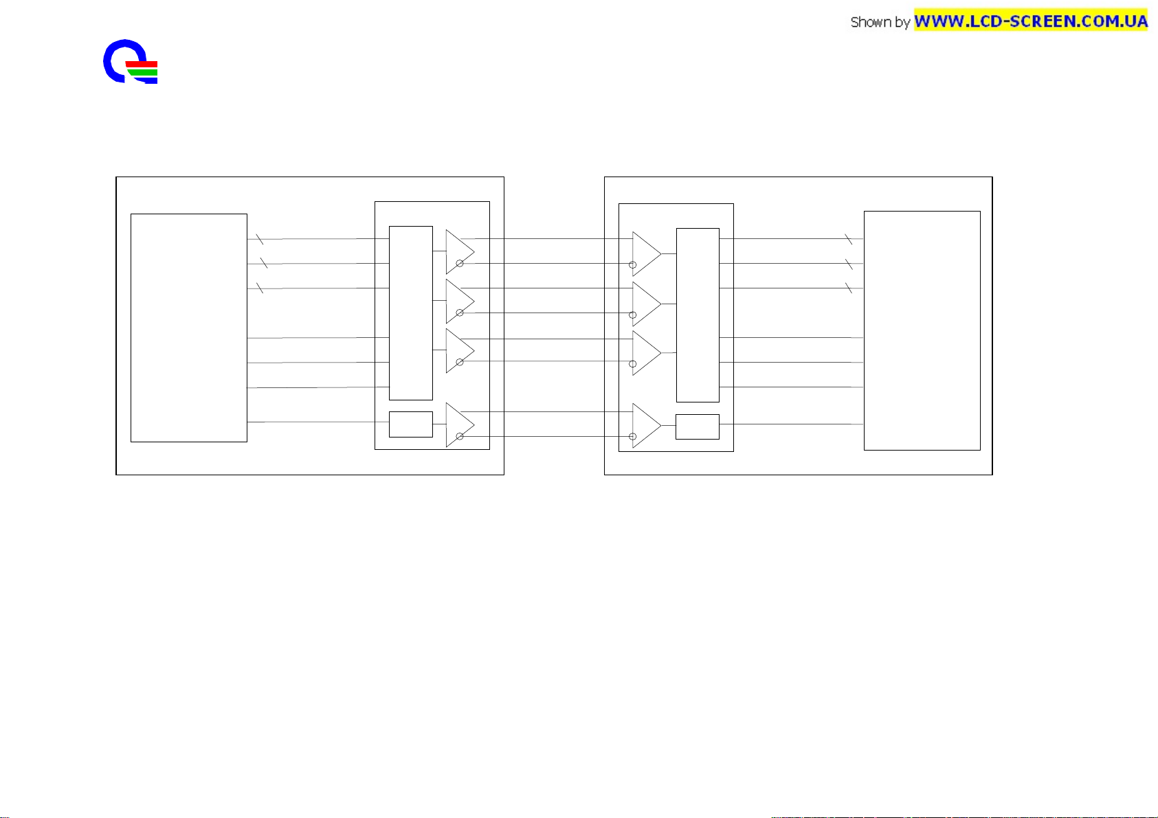
4-2 Interface block diagram
K
QD141X1LH03A2 Page
6
Using receiver:DS90CF364(National semiconductor) Corresponding Transmitter:DS90C363,DS90C383(National semiconductor
(Computer side)
(TFT-LCD side)
)
R0~R5
G0~G5
B0~B5
Hsync
Vsync
Controller
ENAB
CLK
TxIN 0~ 5
6
6
TxIN 6~11
6
TxIN12~17
TxCLK IN
TxIN18
TxIN19
TxIN20
TTL PARALLEL-TO-LVDS
PLL
RXIN0+(6)
RXIN0-(5)
RXIN1+(9)
RXIN1-(8)
RXIN2+(12)
RXIN2-(11)
RXCLKIN+(1
RXCLKIN-
DS90C*363
DS90CF364
PLL
RxOUT0~5
RxOUT6~11
RxOUT12~17
RxOUT18
RxOUT19
LVDS-TO-PARALLEL TTL
RxOUT20
RxCLK OUT
6
R0~R5
6
G0~G5
6
B0~B5
Hsync
Vsync
ENAB
C
Internal circuits
Page 7
4-3. Backlight driving
CN2: BHSR-02VS-1(JST)
Mating connector: SM02B-BHSS-1(JST)
Pin No. Symbol Function
1
V
Power supply for lamp
HIGH
(High voltage side)
2
V
Power supply for lamp
LOW
(Low voltage side)
5. Absolute Maximum Ratings
5-1 LCD module
Parameter Symbol Condition Ratings Unit Remark
Input voltage
VI
Ta=25
0.3 ~ Vcc+0.3
℃ -
QD141X1LH03A2 Page
Note1】
【
V
7
+3.3V supply voltage Vcc Ta=25℃ 0 ~ + 4
Storage temperature Tstg
Operating temperature (Ambient) Topa
-
-
-25 ~ +60
0 ~ +50
V
℃
℃
【Note1】LVDS signals
【Note2】Humidity:95%RH Max. at Ta≦40℃.
Maximum wet-bulb temperature at 39℃ or less at Ta>40℃.
No condensation.
【
Note2】
Page 8

QD141X1LH03A2 Page
6. Electrical Characteristics
6-1.TFT-LCD panel driving Ta=25℃
Parameter Symbol Min. Typ. Max. Unit Remark
Vcc Supply voltage Vcc +3.0 +3.3 +3.6 V
Current dissipation Icc -
Permissive input ripple
V
RP
-
420 TBD mA
-
100 mV p-p Vcc=+3.3V
【
Note2】
【
Note3】
voltage
Differential input High
threshold voltage Low
Input current (High)
Input current (Low)
Terminal resistor
V
TH
V
TL
I
OH
I
OL
R
T
–100 -
-
-
-
-
-
+100 mV V
-
±
-
±
-
100 -
10
10
=+1.2V
CM
mV
μ
A
【
Note1】
VI=2.4V
Vcc=3.6V
A
VI=0V
μ
Vcc=3.6V
Ω
Differential
input
Rush current I
1.5 A Rise time
RUSH
470uS
8
【
Note1】 V
: Common mode voltage
CM
of LVDS driver.
【
Note2】
On-off conditions for supply voltage
0<t1≦10 ms
0<t2≦50 ms
0<t3≦1 s
t4>1 s
Vcc
data
2.8V 2.8V
0.3V 0.3V
t4
t1
Vcc
Vcc
data
t2t3
Vcc-dip conditions
1) 2.5 V≦Vcc<3.0 V
td
V
0
V
5
2
.
3
.
td≦10 ms
2) Vcc<2.5 V
Vcc-dip conditions should also follow the On-off conditions for supply voltage
【
Note3】 Typical current situation : 16-gray-bar pattern.
Vcc=+3.3V
RGB
GS0
RGB
GS4
RGB
GS8
....
RGB
GS56
RGB
GS60
Page 9

QD141X1LH03A2 Page
V
W
6-2. Backlight driving
The backlight system is an edge-lighting type with single CCFT (Cold Cathode
Fluorescent Tube).
The characteristics of the lamp are shown in the following table.
Parameter Symbol Min. Typ. Max. Unit Remark
Lamp current range IL 2.0 4.0 6.0 mArms【Note1】
Lamp voltage V L 660 Vrms
Lamp power
consumption
Lamp frequency FL 30 60 70 kHz
Kick-off voltage Vs
Lamp life time LL 10000
【Note1】 Lamp current is measured with current meter for high frequency as shown
below.
PL
-
-
-
2.7
-
-
-
-
1500 Vrms Ta=25℃
1500 Vrms Ta=0℃ 【Note4】
-
W
hour 【Note5】
【Note2】
【
Note3】
9
1
Module
Inverter
2
A
~
* 2pin is
【
Note2】Calculated Value for reference ( I
【
Note3】Lamp frequency may produce interference with horizontal synchronous
frequency, and this may cause beat on the display. Therefore lamp frequency
shall be detached as much as possible from the horizontal synchronous
frequency and from the harmonics of horizontal synchronous to avoid
interference.
【
Note4】 It is defined at 22pF for the ballast capacitor of a DC/AC inverter.
L × V L)
LO
The voltage above this value should be applied to the lamp for more than 1
second to start-up. Otherwise the lamp may not be turned on.
【
Note5】 Lamp life time is defined as the time when either ① or ② occurs in the
continuous operation under the condition of Ta = 25℃ and I
① Brightness becomes 50 % of the original value under standard condition.
② Kick-off voltage at Ta = 0℃ exceeds maximum value, 1500V rms.
Note) The performance of the backlight, for example life time or brightness, is much
influenced by the characteristics of the DC-AC inverter for the lamp. When you design or
= 6.0 mArms.
L
Page 10

QD141X1LH03A2 Page
order the inverter, please make sure that a poor lighting caused by the mismatch of the
backlight and the inverter (miss-lighting, flicker, etc.) never occur. When you confirm it, the
module should be operated in the same condition as it is installed in your instrument.
7. Timing characteristics of LCD module input signals
7-1. Timing characteristics (This is specified at digital outputs of LVDS driver.)
Data
B
ENAB
Sync
C
D E F
10
A
(Vertical)
Item(symbol)
Vsync cycle (TVA)
Min. Typ. Max. Unit Remark
-
16.667
-
ms Negative
803 806 line
Blanking period(TVB) 35 38
Sync pulse width (TVC) 4 6
-
-
line
line
Back porch (TVD) 0 29 line
Sync pulse width + Back
porch
35 35 35 line
(TVC+TVD)
Active display area (TVE) 768 768 768 line
Front porch (TVF) 0 3
-
line
(Horizontal)
Item(symbol)
Hsync cycle (THA) 19.2 20.677
Min. Typ. Max. Unit Remark
- μs
1260 1344 1408 clock
Blanking period (THB) 236 320
Sync pulse width (THC) 8 136
-
-
clock
clock
Back porch (THD) 0 160 312 clock
Sync pulse width + Back
porch (T
+THD)
HC
1500 - T
HA
296 THA -
1024
clock
Active display area (THE) 1024 1024 1024 clock
Front porch (THF) 8 24
-
clock
Negative
(Clock)
Item Min. Typ. Max. Unit Remark
Frequency
-
65.0 65.0 MHz
【Note1】
Note) In case of lower frequency, the deterioration of display quality, flicker etc., may be
occurred.
Page 11

(Hsync-Vsync Phase difference)
y
y
Vsync
nc
Hs
QD141X1LH03A2 Page
11
Item(symbol) Min. Typ. Max. Unit Remark
Hsync-Vsync Phase difference
)
(T
HV
(Hsync-ENAB Phase difference)
ENAB
nc
Hs
THN
Item Min. Typ. Max. Unit Remark
(THN)
7-2 Display position
Item Standards Beginning Ending Unit Remark
T
HV
1
0
- T
-
HA-THC
312 clock
clock
Horizontal rising edge of ENAB 0 1024 clock
rising edge of Hsync 296 1320 clock
【Note1】
Vertical rising edge of Vsync 35 803 clock
【Note1】 ENAB signal must be fixed to low.
[
Note]
(Horizontal display direction)
When ENAB is fixed low, 296 clock are counted from Hsync negative edge and data from
after are available . If you need other timing, please use ENAB signal.
(Vertical display direction)
35 lines are counted from Vsync negative edge and data from next line are available.
(Note of ENAB signal)
ENAB could not be used for the purpose of the vertical display start timing.
Caution
Image will not be displayed on the right position otherwise.
Page 12

7-3. Input Data Signals and Display Position on the screen
Display position of input data
(H,V)
QD141X1LH03A2 Page
UP
12
D1,DH1
D1,DH2
D1,DH3
D1,DH768
D2,DH1 D3,DH1
D2,DH2
R
G
D1024,DH1
B
D1024,
DH768
Page 13

8. Input Signals, Basic Display Colors and Gray Scale of Each Color
QD141X1LH03A2 Page
13
Colors &
Gray scale Gray
Scale
Black -
Blue -
Basic Color Gray Scale of Red Gray Scale of Green Gray Scale of Blue
Green -
Cyan -
Red -
Magenta -
Yellow -
White -
R0 R1 R2 R3 R4 R5 G0 G1 G2 G3 G4 G5 B0 B1 B2 B3 B4 B5
0 0 0 0 0 0 0 0 0 0 0 0 0 0 0 0 0 0
0 0 0 0 0 0 0 0 0 0 0 0 1 1 1 1 1 1
0 0 0 0 0 0 1 1 1 1 1 1 0 0 0 0 0 0
0 0 0 0 0 0 1 1 1 1 1 1 1 1 1 1 1 1
1 1 1 1 1 1 0 0 0 0 0 0 0 0 0 0 0 0
1 1 1 1 1 1 0 0 0 0 0 0 1 1 1 1 1 1
1 1 1 1 1 1 1 1 1 1 1 1 0 0 0 0 0 0
1 1 1 1 1 1 1 1 1 1 1 1 1 1 1 1 1 1
Data signal
Black GS0 0 0 0 0 0 0 0 0 0 0 0 0 0 0 0 0 0 0
×
GS1 1 0 0 0 0 0 0 0 0 0 0 0 0 0 0 0 0 0
Darker GS2 0 1 0 0 0 0 0 0 0 0 0 0 0 0 0 0 0 0
×
Ø
È
È
È
È
È
È
È
È
Brighter GS61 1 0 1 1 1 1 0 0 0 0 0 0 0 0 0 0 0 0
Ø
GS62 0 1 1 1 1 1 0 0 0 0 0 0 0 0 0 0 0 0
Red GS63 1 1 1 1 1 1 0 0 0 0 0 0 0 0 0 0 0 0
Black GS0 0 0 0 0 0 0 0 0 0 0 0 0 0 0 0 0 0 0
×
GS1 0 0 0 0 0 0 1 0 0 0 0 0 0 0 0 0 0 0
Darker GS2 0 0 0 0 0 0 0 1 0 0 0 0 0 0 0 0 0 0
×
Ø
È
È
È
È
È
È
È
È
Brighter GS61 0 0 0 0 0 0 1 0 1 1 1 1 0 0 0 0 0 0
Ø
GS62 0 0 0 0 0 0 0 1 1 1 1 1 0 0 0 0 0 0
Green GS63 0 0 0 0 0 0 1 1 1 1 1 1 0 0 0 0 0 0
Black GS0 0 0 0 0 0 0 0 0 0 0 0 0 0 0 0 0 0 0
×
GS1 0 0 0 0 0 0 0 0 0 0 0 0 1 0 0 0 0 0
Darker GS2 0 0 0 0 0 0 0 0 0 0 0 0 0 1 0 0 0 0
×
Ø
È
È
È
È
È
È
È
È
Brighter GS61 0 0 0 0 0 0 0 0 0 0 0 0 1 0 1 1 1 1
Ø
GS62 0 0 0 0 0 0 0 0 0 0 0 0 0 1 1 1 1 1
Blue GS63 0 0 0 0 0 0 0 0 0 0 0 0 1 1 1 1 1 1
0 : Low level voltage, 1 : High level voltage
Each basic color can be displayed in 64 gray scales from 6 bit data signals. According to the
Page 14

QD141X1LH03A2 Page
14
combination of total 18 bit data signals, the 262,144-color display can be achieved on the screen.
Ta=25
9. Optical Characteristics
℃
, Vcc=+3.3V
Parameter Symbol Condition Min. Typ. Max. Unit Remark
Viewing
angle
Horizontal
Vertical
range
Contrast ratio
Response Rise
time Decay
Chromaticity of x
white y
Luminance of
white
【
Note4】 Y
θ21,θ22 CR>10 45 -
θ
11 10 -
θ
12 30 -
CR
n
CR
o
τ
r
τ
d -
Y
L1
L2
θ=0°
Optimum
viewing
θ=0°
150 -
-
angle
-
0.273 0.313 0.354
0.289 0.329 0.369
120 - Cd/m
120 150 - Cd/m
-
-
-
-
300 -
15 ms
Deg.
Deg.
Deg.
Note1,4
【
Note2,4
【
Note3,4
【
30 ms
Note4】
【
2
IL = 4
FL=60kHz
2
IL =
6.0mArms
】
】
】
.0mArms
FL=60kHz
White Uniformity δ
The measurement shall be executed 30 minutes after lighting at rating. (typical condition :
※
W
-
-
1.45
【
Note5
】
IL = 4.0 mArms)
The optical characteristics shall be measured in a dark room or equivalent state with the
method shown below.
Page 15

Photodetector (BM-5A:TOPCON)
QD141X1LH03A2 Page
15
TFT-LCD
module
Field=
Fig.3 Optical characteristics measurement method
2°
400
Center of the screen
mm
LCD
panel
Page 16

【
Note1】Definitions of viewing angle range:
【
Note2】Definition of contrast ratio:
The contrast ratio is defined as the following.
QD141X1LH03A2 Page
16
Luminance (brightness) with all pixels white
Contrast Ratio (CR)=
Luminance (brightness) with all pixels black
【
Note3】Definition of response time:
The response time is defined as the following figure and shall be measured by
switching the input signal for "black" and "white" .
【
Note4】This shall be measured at center of the screen.
【
Note5】Definition of white uniformity:
White uniformity is defined as the
following with five measurements
(A~E).
Maximum Luminance of five points (brightness)
δw=
Minimum Luminance of five points (brightness)
768 pixel 512256
D A
C
E B
192
384
576
Pixel
Page 17

QD141X1LH03A2 Page
10. Display Quality
The display quality of the color TFT-LCD module shall be in compliance with the Incoming
Inspection Standard.
11.Handling Precautions
a) Be sure to turn off the power supply when inserting or disconnecting the cable.
b) Be sure to design the cabinet so that the module can be installed without any extra
stress such as warp or twist.
c) Since the front polarizer is easily damaged, pay attention not to scratch it.
d) Wipe off water drop immediately. Long contact with water may cause discoloration or
spots.
e) When the panel surface is soiled, wipe it with absorbent cotton or other soft cloth.
f) Since the panel is made of glass, it may break or crack if dropped or bumped on hard
surface. Handle with care.
g) Since CMOS LSI is used in this module, take care of static electricity and injure the
17
human earth when handling.
h) Observe all other precautionary requirements in handling components.
i) This module has its circuitry PCBs on the rear side and should be handled carefully in
order not to be stressed.
j) Laminated film is attached to the module surface to prevent it from being scratched .
Peel the film off slowly just before the use with strict attention to electrostatic charges.
Ionized air shall be blown over during the action. Blow off the 'dust' on the polarizer by
using an ionized nitrogen gun, etc..
K) Black PET sheet covers some electric components and handle with special care to
avoid mechanical stress and shock on this PET surface.
L) Mounting screw hole can stand torque 1.3~1.5 Kgf-cm.
Page 18

12. Reliability test items
Test item Conditions
No.
1 High temperature storage test Ta = 60℃ 240h
2 Low temperature storage test Ta = -25℃ 240h
QD141X1LH03A2 Page
18
3 High temperature
& high humidity operation test
Ta = 40℃ ; 95 %RH 240h
(No condensation)
4 High temperature operation test Ta = 50℃ 240h
(The panel temp. must be less than 60℃)
5 Low temperature operation test Ta = 0℃ 240h
6 Vibration test
(non- operating)
Frequency: 1. 10~57Hz/Vibration width (one
side) 0.075mm
2. 58~500Hz/Gravity 9.8m/s
Sweep time : 11 minutes
Test period : 3 hours
(1 hour for each direction of X,Y,Z)
7 Shock test
(non- operating)
Max. gravity : 490 m/s2
Pulse width : 11 ms, sine wave
Direction : ±X,±Y,±Z
once for each direction.
2
13.Others
1) Lot No. Label:
Serial number Product Name
HFC1171000001 QD141X1LH03 Rev.A
Ver.: xxxx
QDI internal
control version No.
Serial Number Bar Code
2) Adjusting volume has been set optimally before shipment, so do not change any
adjusted value. If adjusted value is changed, the specification may not be satisfied.
3) Disassembling the module can cause permanent damage and should be strictly
avoided.
4) Please be careful since image retention may occur when a fixed pattern is displayed
for a long time.
5) If any problem occurs in relation to the description of this specification, it shall be
resolved through discussion with spirit of cooperation.
Page 19

QD141X1LH03A2 Page
14. Attachment
Incoming Inspection Standards for TFT-LCD Modules
1) Scope
These incoming inspection standards shall apply to TFT-LCD modules (hereinafter called
“Module”) supplied by QDI Corporation (hereinafter called “Seller”) to Quanta
(hereinafter called the “Buyer”).
2) Incoming inspection
The Buyer shall have the right to conduct at its own cost and expense, an incoming
inspection of the Module’s at the destination specified in the relevant bills of landing in
accordance with the Module’s specifications separately agreed upon and the inspection
standard set forth in this Article. The Buyer shall notify the Seller writing of a result of
such inspection judgment (acceptance or rejection) in accordance with the said
19
inspection standard within 40 days after the date of the bills of landing. Should the Buyer
fail to so notify the seller within the said 40 days period, the Buyer’s right to reject the
Module’s shall then lapse, and the said Module’s shall be deemed to have been accepted
by the Buyer.
3) Method of incoming inspection
Unless otherwise agreed in writing, the method of incoming inspection shall be in
accordance with a sampling inspection based on MIL-STD-105E.
4) Classification of defects
Defects are classified as major defect and a minor defect according to the degree of
defect defined herein.
a) major defect
A major defect is a defect that is likely to result in failure, or to reduce materially
the usability of the product for its intended purpose.
b) Minor defect
A minor defect either is a defect that is not likely to reduce materially the usability
of the product for its intended purpose, or is a departure from an established
having little bearing on the effective use or operation of the product.
Specific criteria of judgment on major and/or minor defects or otherwise shall be in
accordance with the attached “Classification of Defect.”
5) Acceptable quality level (“AQL”)
The AQL for major and minor defects shall be respectively set forth below.
a) Major defects : AQL :0.4
Page 20

QD141X1LH03A2 Page
b) Minor defects : AQL:1 Based on overall evaluation
6) Method of sampling inspection
a) Lot size : Quantity per shipment lot per mode
b) Sampling type : Normal inspection, Single sampling
c) Inspection level : II
d) Sampling table : Table in MIL-STD-105E
e) Inspection conditions : The inspection conditions shall be as in the LCD
specifications. The environmental conditions and the visual inspection shall be as
follows:
(i) The environmental conditions
Room temperature: 20-25°C
Humidity: 65±20%RH
(ii) The external visual inspection: The inspection shall be conducted by using a
20
single 20W fluorescent lamp for illumination and the distance between the
MODULE and the eyes of the inspection shall be 35CM±5CM.
7) Determination of acceptability and subsequent disposal
If the number of defects found in the sample Module’s from the lot is equal to or less
than the applicable acceptance level, the lot shall be accepted.
If the number of defects is greater than the applicable acceptance level, the lot shall be
rejected. The Buyer shall inform the Seller of detailed result of such inspection within the
time period stipulated in Article 2.
The disposal is as follows:
a) Accepted lot
An acceptance under the above incoming inspection shall constitute an acceptance
by the Buyer of such lot of the Module’s in terms of the landed quality thereof.
b) Rejected lot
If a lot of PRODUCTS is rejected under the above incoming inspection due to any
defects for which the Seller is responsible and such a fact is clearly confirmed by
the Sellers, the Seller shall exercise one of the following three options. This must
be determined with mutual consent and shall be confirmed by the Seller. The best
choice of the options shall be left to the Seller’s discretion and the Seller shall
advise the Buyer of its choice not later than two weeks of receipt of the Buyer’s
advance:
(1) The Buyer shall return the defective lot to the place to be designated by the Seller
and Seller shall screen all of the PRODUCTS in the lot and repair defective
PRODUCTS.
(2) The Seller shall screen all of the PRODUCTS in the lot and repair defective products
Page 21

QD141X1LH03A2 Page
within a reasonable time period at the Buyer’s facility.
(3) The Buyer shall screen the entire lot for the good modules at the expense of the
Seller to be separately agreed upon. The rejected PRODUCTS shall be returned to
the place to be designated buy the Seller.
8) External inspection
Inspection item Criteria Reject count(N)
21
Black spot ,White spot,
Foreign circular
Material Dent &bubble
L:length; W:width(mm)
Average Diameter:D
a+b
D =
2
a
b
D>0.35mm N>1
D>0.15mm N>4
D<0.15mm Don’t care
Minimum distance between defects :10mm
L>2.0 N>1 Scratches ,lint
N>
0.01<W<0.05 L≦2.0
3
Length:L
L =Lon
est
oint
W
L
*1 The external visual inspection: The inspection shall be conducted by using a single
20W fluorescent lamp for illumination and the distance between the MODULE and the
eyes of the inspector shall be 35 ㎝ or more.
* The area for external inspection is active area plus 1.0mm width. (Upper, Low er, Left
and Right)
Page 22

QD141X1LH03A2 Page
9) Dot defect
(1) Inspection Conditions [Visual inspection]
Viewing distance : 35 ㎝
Ambient illumination : 300 to 700Lux ( Standard 500Lux )
Ambient temperature : 20-25℃
Light source condition : Based on the specification
Note: Viewing angle : The surface of the MODULE and the eyes of the inspector
shall be 90 degrees.
(2) Definition
a) Bright dot
The sub-pixel can been seen when using the 5% ND-Filter
22
b) Scratches on the color filter (Bright dot count)
Count: defect area > 1/4 dot
No count: defect area < 1/4 dot
(3) Bright dots (Acceptable)
Green/Red/Blue dots:When the MODULE lights, dots appear bright in display at
black picture position.(V0)
Check pattern Total Quantity
Black picture
Position
2 adjacent ….. 1 pair MAX
Green Bright dots 2 adjacent ….. Nothing
Defect distance ….. more than 15mm
(4) Black dots (Acceptable)
Black dots : When the MODULE lights, dots appear black in display at
≦4
Green+Blue+Red picture position.
Check pattern Total
Green+Blue+Red
Picture position
Two joined dots ….. 2 pair MAX
Defect distance ….. more than 5mm
Three joined bright dots must be nil
Three picture position total
8 MAX
Page 23

QD141X1LH03A2 Page
(5) Total dot defect ( Black & Bright )
Total dot defects:It is possible if accept count is the counts of Bright and Dark
dots at V24 gray screen
23
Check pattern Total Quantity
V24
8 MAX
gray screen
10) Display non-uniformity
There should be no distinct non-uniformity visible through 5﹪transparency of filter.
Viewing distance :35cm
Ambient illumination :300 to 700 Lux(standard 500Lux)
Ambient temperature :20-25℃
Light source condition :Based on the specification.
Note : Viewing angle : The surface of the Module and the eyes of the inspector shall be
90 degrees.
11) Others
If some problems arise about mentioned items in this document and other items, the
user of the TFT-LCD module and QDI will cooperate and make efforts to solve the
problems with mutual respect and good will.
 Loading...