

Page 1

JM3 Power--
JM3 Power
1. To know JM3 Power-Up Sequence.
2. More easy to find out the root-cause if system
Lock-Up of No-Power.
3. To realize each step before BIOS is working.
4. Summarized preliminary Power-Up sequence
diagram.
up Sequence
up Sequence
5. Power-up sequence after POWER_SW# in the
Nutshell.
Page 2
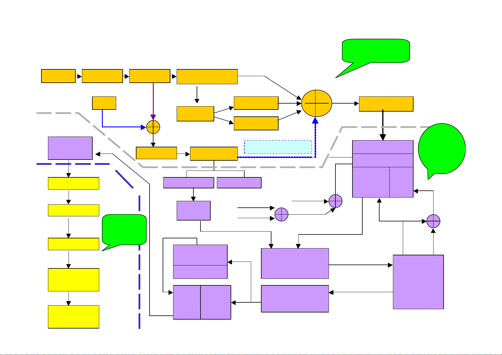
Block
High Volt.
Section
DCIN+ DC_IN+
PCIRST#
CPURST#
Banias CPU
Montara GM
+DC_IN
FSB
HUB-LINK
12V
System on, Bat
powered only
BUS
Adapter is
alive
RBAT_7.2V
Section
ICH4
SDC_IN+
V-CHG
charging
VCCRTC
RTCRST#
1715PWROK
Charging
Charging
+RTCSRC
+RTC_PWR5V+RTC_PWR3_3V
PBATT+
SBATT+
Warm swap only
LIVE_ON_BATT
LIVE_ON_BATT
ACAV_IN
THERM_STP#
ALWON
SUSPWROK
shutdown
PWR_SRC
D/D Power
+3VALW,5VALW
+5VSUS,
+1_5VSUS
+2_5VSUS
+3VSUS
SUS_ON
PWRGOOD,
D/D
Section
AUX_EN
LPC
SIO
(MACALLEN)
X-BUS
Flash ROM
(8M bit)
+VCC1_2_GMCH,
VTT,
12V
Delay
(3~12mS)
DELAY_IMVP_PWRGD
VHCORE
(IMVP IV)
RUNPWROK
ICH4
+5VRUN, +3VRUN,
+1_5VRUN, +2_5VRUN,
+1_8VRUN
SLP_S3#
MACALLEN
(LPC47N254)
RUN_ON
Page 3
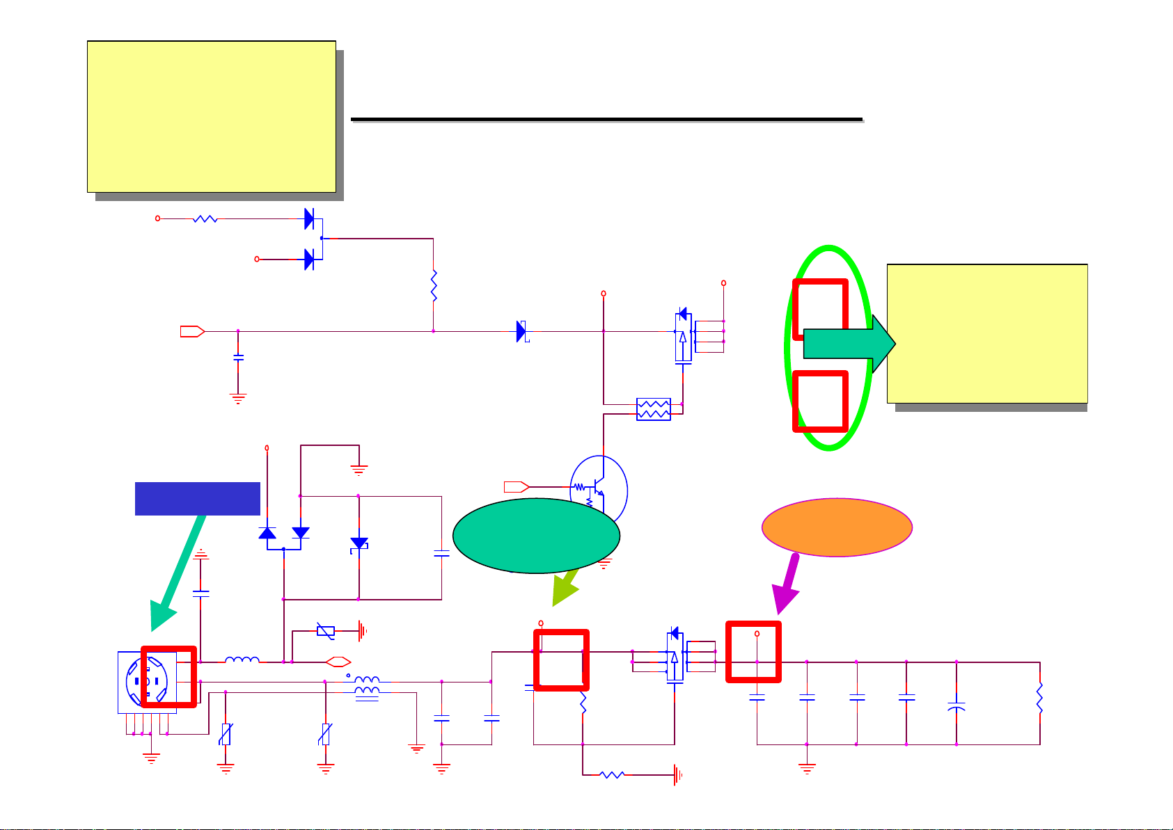
Binchuan:
Binchuan:
(1).ADP-IN
(1).ADP-IN
(2).+DC_IN
(2).+DC_IN
(3).DC_IN+
(3).DC_IN+
Schematic page 29
Schematic page 29
DC_IN+
RBAT_7.2V30
R380
12
15K
Near JDCIN1
ADP-IN (1)
Near JDCIN1
C856
100P_50V
JDCIN1
POWER_JACK
H
98765
4
VZ0603M260APT
1
2
3
L27 BLM11B102S
12
D13R_VCC
+12V
C208
1000P
+3VALW
D44
DA204U
DCIN+
RV2
2
1
1
3
DCIN-
ADAPTER--
ADAPTER
D24
3
RB715F
TRACE:20MIL TRACE:20MIL
2
RV3
1 2
VZ0603M260APT
PS_ID 22,34
2
1
FL1 CM1922
12
RV1
VZ0603M260APT
SBATT_CH
21
D45
UDZ3.6B_NC
3
4
CM1922
12
R379
10K
2 1
1N5819HW
SYS_SUSPEND21
C855
+DC_IN (2)
100P_50V
Near JDCIN1
C857
.1U_50V
C858
0.01U_50V
D25
+DC_IN
C35
.47U_0805
25V
2
H
+RTCSRC
47K
12
Q49_G
3
47K
1
R27
240K
R22 47K
1 2
IN(P29)
IN(P29)
PWR_SRC
Q48
FDG316P
4
RP97
2
4
4P2R-S-100K
Q46
DTC144EUA
TRACE:20MIL
3
1
3
6
5
2
1
DC_IN+ (3)
Q37
1
2
3
FDS6679
4
8
7
6
5
DC_IN+
H
C38
.01U
H
L
C41
.1U_50V
Binchuan:
Binchuan:
H : High Level.
H : High Level.
L : Low Level
L : Low Level
And so on.
And so on.
12
C357
.1U_50V
C42
.1U_50V
+
C363
10U_25V_1210
12
R542
4.7K
Page 4
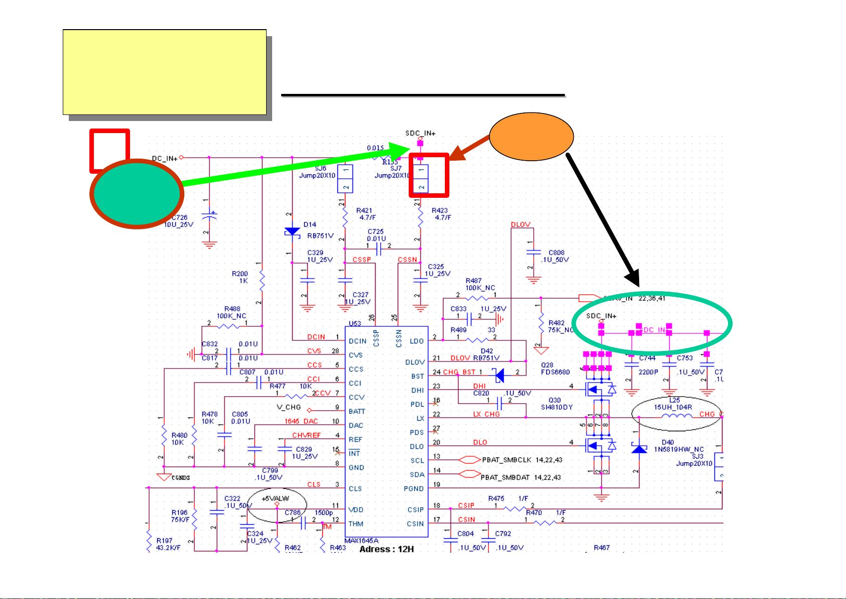
Binchuan:
Binchuan:
(4). DC_IN+ to SDC_IN+
(4). DC_IN+ to SDC_IN+
Schematic page 37
Schematic page 37
H
DC_IN+
SDC_IN+(P31)
SDC_IN+(P31)
SDC_IN+(4)
H
Page 5
Binchuan:
Binchuan:
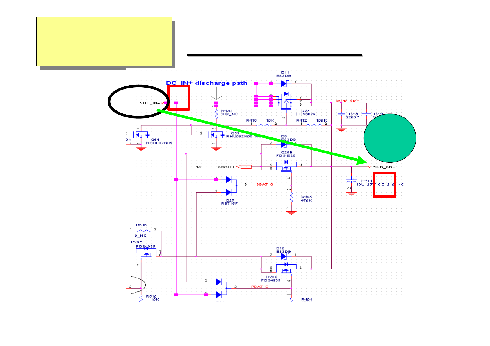
(5). SDC_IN+ to PWR_SRC
(5). SDC_IN+ to PWR_SRC
Schematic page 36
Schematic page 36
PWR_SRC(P36)
PWR_SRC(P36)
H
PWR_SRC
H
Page 6
Binchuan:
TRACE:20MIL
Binchuan:
+RTCSRC supply +RTC_PWR5V
+RTCSRC supply +RTC_PWR5V
and +RTC_PWR3_3V
and +RTC_PWR3_3V
DC_IN+
RBAT_7.2V30
R380
15K
D13R_VCC
12
+12V
C208
1000P
D24
2
1
RB715F
+
RTCSRC(P41,43)
+
RTCSRC(P41,43)
3
SBATT_CH
12
TRACE:20MIL TRACE:20MIL
R379
10K
SYS_SUSPEND21
+RTCSRC
D25
2 1
1N5819HW
2
+RTCSRC
47K
47K
H
3
Q48
FDG316P
4
RP97
2
4
4P2R-S-100K
Q46
DTC144EUA
3
1
3
PWR_SRC
6
5
2
H
1
PWR_SRC
+RTCSRC
+RTCSRC
R382 10K
H
C644
.1U_50V
1 2
C645
1U_25V
U35 MAX1615
1
IN
SOT23-5
OUT
5/3#
GNDSHDN
1
+RTCSRC
+RTCSRC
H
3
4
25
+RTC_PWR3_3V
C646
+RTC_PWR3_3V
10U_10V
H
R394 10K
1 2
C661
.1U_50V
C662
1U_25V
U39 MAX1615
1
IN
SOT23-5
OUT
5/3#
GNDSHDN
H
3
4
25
+RTC_PWR5V
C654
10U_10V
+RTC_PWR5V
Page 7
Binchuan:
about Adaptor(Present).
Binchuan:
ACAV_IN will be
ACAV_IN will be
generated after
generated after
+RTC_PWR5V.
+RTC_PWR5V.
DC_IN+ (3)
H
ACAV_IN(P37)
+RTC_PWR5V
R468
75K/F
R471
12.7K/F
DC_IN+
12
12
1
12
R459
1K
R465 10K
1 2
R464 1M
1 2
U52
LM431SACMF
3 2
+RTC_PWR5V
2
12
H
1
Q61
39063
ACAV_IN 22,36,41
ACAV_IN
R458
100K
H
Binchuan:
Binchuan:
ACAV_IN generate to notice SIO
ACAV_IN generate to notice SIO
about Adaptor(Present).
Page 8
Binchuan:
Binchuan:
MAX1999 use LDO to
MAX1999 use LDO to
output +5VALW&+3VALW
output +5VALW&+3VALW
while U50 pin 17(VCC)
while U50 pin 17(VCC)
has Power Source and
has Power Source and
Pin 6 is at Logic H.
Pin 6 is at Logic H.
PWR_SRC
+3
+3
VALW&+5VALW(P41)
VALW&+5VALW(P41)
H
H
H
THERM_STP#
VCC
SHDN
H
Page 9
Binchuan:
Binchuan:
(6).As soon as +RTC_PWR3_3V on, then
(6).As soon as +RTC_PWR3_3V on, then
RTCRST# will be from Low ?High.
RTCRST# will be from Low ?High.
(Reset CMOS)
(Reset CMOS)
RTCRST#(P9)
RTCRST#(P9)
VCCRTC
+RTC_PWR3_3V
Binchuan:
Binchuan:
CLK_32KX1/X2 must
CLK_32KX1/X2 must
be generated, it’s for
be generated, it’s for
RTCCLK units(ICH4)
RTCCLK units(ICH4)
using to generate
using to generate
SLP_S3# &SLP_S5#.
SLP_S3# &SLP_S5#.
H
H
H
RTCRST#
ICH4
OSCILLATION
Page 10
Binchuan:
Binchuan:
(A).POWER_SW# generate
(A).POWER_SW# generate
the POWER_SIO#, and If
the POWER_SIO#, and If
MACALLEN(SIO) is alive
MACALLEN(SIO) is alive
then it’ll assert SUN_ON to
then it’ll assert SUN_ON to
MAX1999 (3/5VSUS)
MAX1999 (3/5VSUS)
H-L-H
POWER_SW#
POWER_SIO#
POWER_SW#27,28
PWRSW_SIO#21
H-L-H
POWER_SW#(P41,P2
POWER_SW#
D26
2 1
RB751V
LIVE_ON_BATT22
+RTC_PWR5V
C650
.1U
ACAV_IN22,36,37
12
R391
10K
R397 100K
1 2
+RTC_PWR5V
5
1 6
+RTC_PWR5V
5
2
1
1 2
U36A
7WZ14
C657
.1U
NC7ST32
1)
U40
4
+RTC_PWR5V
5
2
1
C658
1 2
.1U
U41
7SH32
4
H-L-H
SUS_ON
MACALLEN(SIO)
H
Page 11
Binchuan:
With respect of MAX1999, the SHDN# pin need
SUS_ON signal to generate 3/5/12V.
Binchuan:
THERM_STP# is OD and will be
THERM_STP# is OD and will be
generated its function after +3VSUS.
generated its function after +3VSUS.
MAX1999(P41)
SHDN#
MAX1999
ON3
ON5
SUS_ON
SUS_ON
Keep ‘H’
H
H
H
H
Binchuan:
Binchuan:
With respect of MAX1999, the SHDN# pin need
to at Logic ‘H’ and Enable ON3 & ON5 from
to at Logic ‘H’ and Enable ON3 & ON5 from
SUS_ON signal to generate 3/5/12V.
Page 12
Binchuan:
Binchuan:
SUS_ON turn on +3/5VSUS power.
SUS_ON turn on +3/5VSUS power.
While MAX1999 stable then it
While MAX1999 stable then it
generate SUSPWROK_5V.
generate SUSPWROK_5V.
3/5/12V(P41)
15V
+5VSUS
+3VSUS
H
MAX1999
H
H
+12V
H
H
SUSPWROK_5V
Page 13

Binchuan:
force POWER
SHUT DOWN
.
Binchuan:
+3VSUS? THERM_STP# at Logic ‘H’.
+3VSUS? THERM_STP# at Logic ‘H’.
Guardian Thermal IC control currently
Guardian Thermal IC control currently
System Thermal status.
System Thermal status.
THERMDA2
THERM_STP#(P28)
ATF_INT# 21
THERMDC2
R80
+3VSUS
C104
49.9/F
.1U
+RTC_PWR3_3V
C115
.1U
+3VSUS
Notes:
Vset=(Tp-75)/16
Where Tp=75 to
106 degree C
C461
.1U
Set trip point=90 degree c
Vset = (90-75)/16=
0.9375 V
Guardian temp-tolerance= +/-3 degree C
R268
30.1K/F
R269
12.1K/F
DAT_SMB14,22,25
CLK_SMB14,22,25
THERMDA
THERMDC
SUSPWROK9,35
+3V_PWROK35
C852
2200P
C114
2200P
POWER_SW#27,41
DAT_SMB
CLK_SMB
R267
1K
R92
1K
R265
1K
THERMTRIP1#
R86
100K
R87
100K
R266
1K
U4
Thermal IC
1
THDAT_SMB
2
THCLK_SMB
13
SMBADDRSEL
18
REM_DIODE2_P
17
REM_DIODE2_N
4
+3VSUS
11
VSUS_PWRGD
10
+RTC_PWR3V
5
+3V_PWROK#
21
POWER_SW#
6
THERMTRIP1#
7
THERMTRIP2#
8
THERMTRIP3#
22
VSET
14
HW_LOCK#
3 12
VSS INTRUDER#
+3VSUS
EMC6N300
ATF_INT#
VCP
RESSERVED
REM_DIODE1_N
REM_DIODE1_P
THERMTRIP_SIO
THERM_STP#
+5VSUS
9
VCP
23
C105
2200P
16
19
20
15
24
Q42
+3VALW
R330
100K
RT1 should be placed near DDR.
R317
2.21K/F
12
RT1
TH11-3H103FT
10Kohm
t
@25 degree C
31
2
RHU002N06
C110
2200P
Put 2200P close to Guardian.
+5VSUS
R309
10K
THERMTRIP_SIO22
THERM_STP#41
INTRUDER#9
5V_CAL_SIO# 21
Place under CPU
Q17
1
2
3
3904
R534
8.2K
Q85
2
3904
THERMTRIP1#
3R535 2.2K
1
.1U
C853
Binchuan:
Binchuan:
C853 needs to be placed
While THERM_STP# to be
near Guardian IC.
While THERM_STP# to be
generated will cause MAX1999
generated will cause MAX1999
VTT
THERMTRIP#2,9
force POWER SHUT DOWN.
Page 14

Binchuan:
Binchuan:
When +5VSUS supply SC1486 then it’ll
When +5VSUS supply SC1486 then it’ll
generate +2_5VSUS,SMDDR_VTERM
generate +2_5VSUS,SMDDR_VTERM
and 1.25V_PWRGD & 2.5V_PWRGD.
and 1.25V_PWRGD & 2.5V_PWRGD.
+2_5VSUS
H
1.25V_PWRGD(P40)
+5VSUS
H
2.5V_PWRGD
H
SMDDR_VTERM
(1.25V)
H
1.25V_PWRGD
H
SC1486
Page 15
Binchuan:
Binchuan:
(C). When +5VSUS supply
(C). When +5VSUS supply
MAX1715 then it’ll generate
MAX1715 then it’ll generate
+1.5VSUS,+2.5VSUS and
+1.5VSUS,+2.5VSUS and
1715SUSOK.
1715SUSOK.
VTT(1.05V)
H
1715PWROK(P42)
+5VSUS
H
+VCC1_2_GMCH(1.2V)
H
MAX1715
1715PWROK
H
Page 16

Binchuan:
Binchuan:
SUSPWROK_5V as +3/5VSUS
SUSPWROK_5V as +3/5VSUS
is ok. Then it will connect with
is ok. Then it will connect with
AND-Gate with SUS_ON then
AND-Gate with SUS_ON then
AND with 2.5V_PWRGD to
AND with 2.5V_PWRGD to
produce SUSPWROK.
produce SUSPWROK.
SUSPWROK(P35)
Keep Away from high speed buses
1.25V_PWRGD40
RUN_ON21,23,39,44
SUSPWROK_5V
SUSPWROK_5V41
SUS_ON21,40,41
+3VSUS
5
2
1
U32
7SH08
H
12
1715_1.5V_PWRGOOD39
+3VSUS
5
2
1
U31
7SH08
R346
100K
C602
.1U
4
+3VSUS+3VRUN
5
1 6
7WZ14
C613
.047U
U28A
4
C595
.1U
H
+3VSUS
5
2
1
U27
7SH08
+3V_PWROK 28
+3VSUS
U28B
5
3 4
7WZ14
2.5V_PWRGD40
+3VSUS
C601
.1U
14
U30A
1
2
74AHC08
4
3
U30B
4
5
74AHC08
6
SUSPWROK 9,28
RUNPWROK 22,38,41,42
H
U30C
H
10
9
8
74AHC08
SUSPWROK
Page 17

Binchuan:
Binchuan:
RTCRST# inactive to SUSCLK
RTCRST# inactive to SUSCLK
running,SLP_S3#,SLP_S5#
running,SLP_S3#,SLP_S5#
inactive.
inactive.
SUSPWROK
SLP_S3#,SLP_S5#(P09)
RSMRST#
H
ICH4
ICH4
L?H
SLP_S3#
SLP_S5#
Binchuan:
Binchuan:
RSMRST# used for
RSMRST# used for
resetting the resume
resetting the resume
power plane logic.
power plane logic.
Binchuan:
Binchuan:
Inactive SLP_S3# signal
Inactive SLP_S3# signal
detected by MACALLEN(SIO).
detected by MACALLEN(SIO).
Logical Level L? H .
Logical Level L? H .
Page 18

Binchuan:
Binchuan:
(D). SLP_S3# generate
(D). SLP_S3# generate
RUN_ON to turn on RUN
RUN_ON to turn on RUN
Power plane.
Power plane.
P.S.: MACALLEN(SIO)
P.S.: MACALLEN(SIO)
ignore the SLP_S5# signal
ignore the SLP_S5# signal
RUN_ON(P21)
SLP_S3#
H
H
MACALLEN(SIO)
RUN_ON(D)
Page 19

+1.5VSUS
H
MAX1715 1.8VRUN(P39)
+5VSUS
H
+1.8VRUN
H
RUN_ON
H
MAX1715
H
1715_1.5 V_PWRGOOD
Page 20

RUN POWER(P44)
RUN_ON_5V#
RUN_ON_5V#
RUN_ON21,23,35,39
RUN_ON
Binchuan:
Binchuan:
RUN_ON turn on all RUN POWER.
RUN_ON turn on all RUN POWER.
RUN_ON enable as below:
RUN_ON enable as below:
1.1. +3VRUN, +5VRUN, +1_5VRUN, +3VRUN, +5VRUN, +1_5VRUN,
1. +3VRUN, +5VRUN, +1_5VRUN,
+2_5VRUN(P44)+2_5VRUN(P44)
+2_5VRUN(P44)
2.2. +1_8VRUN (P39)+1_8VRUN (P39)
2. +1_8VRUN (P39)
H
H
2
12
31
RHU002N06
R472
100K
2
Q69
12OUT +5VRUN+5VALW
12
31
RHU002N06
Q74
100K
C826
4700PF
H
+5VSUS
+3V_SRC
+1_5VSUS
Q2
SI3456DV
6
5
2
1R481
Q56
6
5
2
1 C763
Q67
SI3456DV
6
5
2
1
3
12
3
3
4
R1
470K_NC
4
SI3456DV
4
H
+3VRUN
H
+1_5VRUN
H
C31
4.7U_10V
4.7U_10V
C819
4.7U_10V
+5VRUN
+3VRUN
+1_5VRUN
+2_5VSUS +2_5VRUN
NDS351AN
Q73
3
2
ID = 300mA(Max).
Rds= 1.0 Max @Vgs=10V.
Rds= 0.7 (Typ.)@Vgs=10V.
1
C822
H
+2_5VRUN
1U_10V
Page 21

Binchuan:
Binchuan:
RUNPWROK turns on CPU
RUNPWROK turns on CPU
VCORE POWER.
VCORE POWER.
RUNPWROK(P35)
Keep Away from high speed buses
1715_1.5V_PWRGOOD
+3VSUS
5
H
2
1
U32
7SH08
1.25V_PWRGD40
RUN_ON21,23,39,44
RUN_ON & 1.25V_PWRGD
SUSPWROK_5V41
SUS_ON21,40,41
12
1715_1.5V_PWRGOOD39
4
+3VSUS
5
2
1
U31
7SH08
R346
100K
C602
.1U
+3VSUS+3VRUN
5
1 6
7WZ14
C613
.047U
U28A
4
C595
.1U
H
+3VSUS
5
2
1
H
+3VSUS
U27
7SH08
2.5V_PWRGD40
+3V_PWROK 28
U28B
5
3 4
7WZ14
4
H
H
+3VSUS
14
U30A
1
2
74AHC08
U30C
9
10
74AHC08
C601
.1U
3
RUNPWROK
U30B
4
5
74AHC08
H
6
H
SUSPWROK 9,28
RUNPWROK 22,38,41,42
SUSPWROK
8
Page 22
Binchuan:
from MACALLEN(SIO).
Binchuan:
DBR#(Date Bus Reset) is used only in
DBR#(Date Bus Reset) is used only in
processor systems where no debug port
processor systems where no debug port
is implemented on system board. (Can
is implemented on system board. (Can
be drive as system reset.)
be drive as system reset.)
+3VSUS
Remove one gate
12
R339
10K_NC
DBP#
R340
DBR#2,9
1 2
0
H
+3VSUS
12
R345
IMVP_PWRGD(P35)
+3VSUS
C597
.047U
5
2
1
U26
7SH08
U30D
4
12
13
74AHC08
H
IMVP_PWRGD
11
IMVP_PWRGD 5,9,12
IMVP_PWRGD
1715PWROK
1715PWROK9,42
10K
H
RESET_OUT#22
RESET_OUT#
H
Binchuan:
Binchuan:
RESET_OUT# comes
RESET_OUT# comes
from MACALLEN(SIO).
Page 23
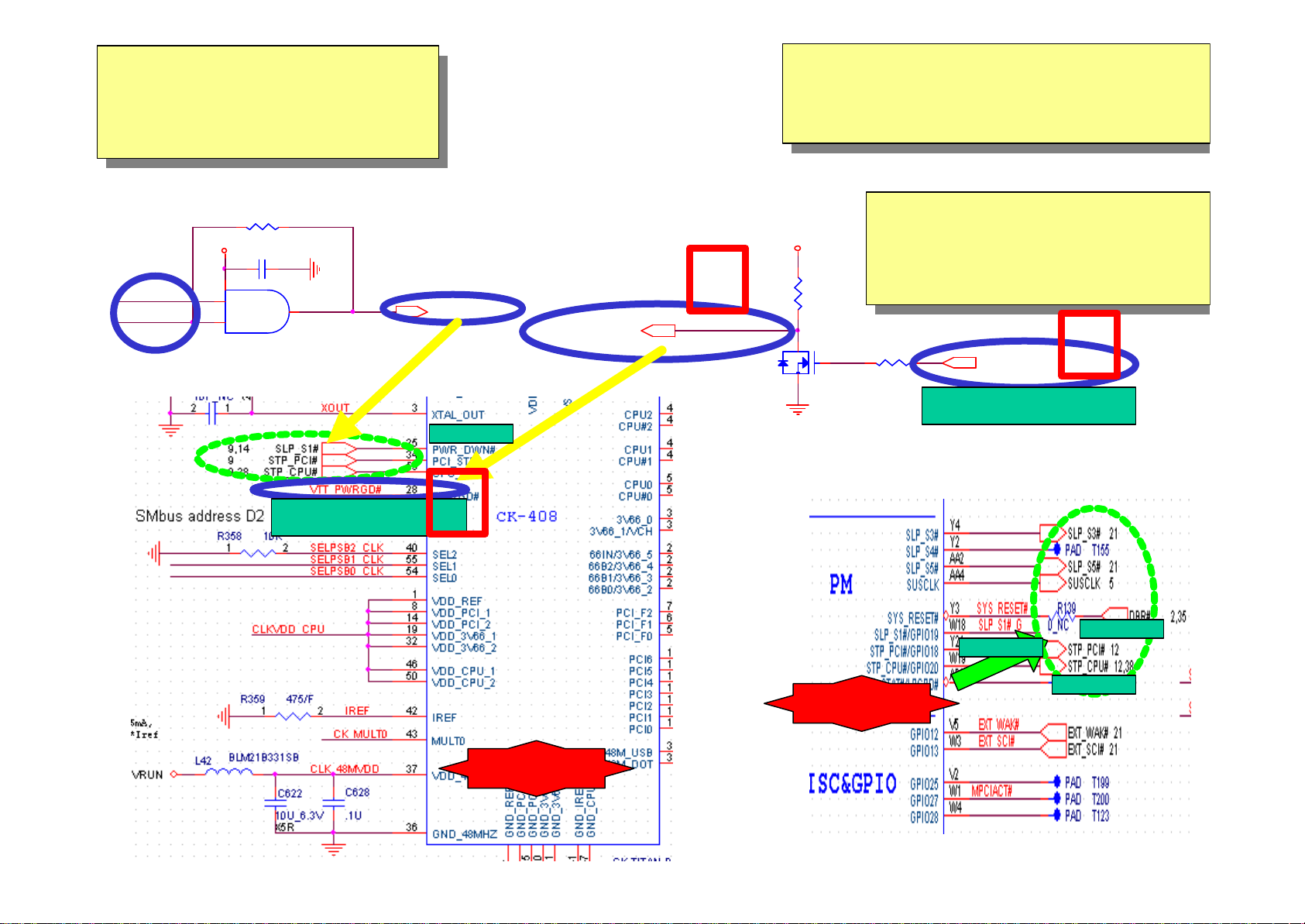
Binchuan:
Binchuan:
SLP_S3# & SLP_S1_G# inactive
SLP_S3# & SLP_S1_G# inactive
generate SLP_S1# inactive, so it
generate SLP_S1# inactive, so it
causes CK-408 active.
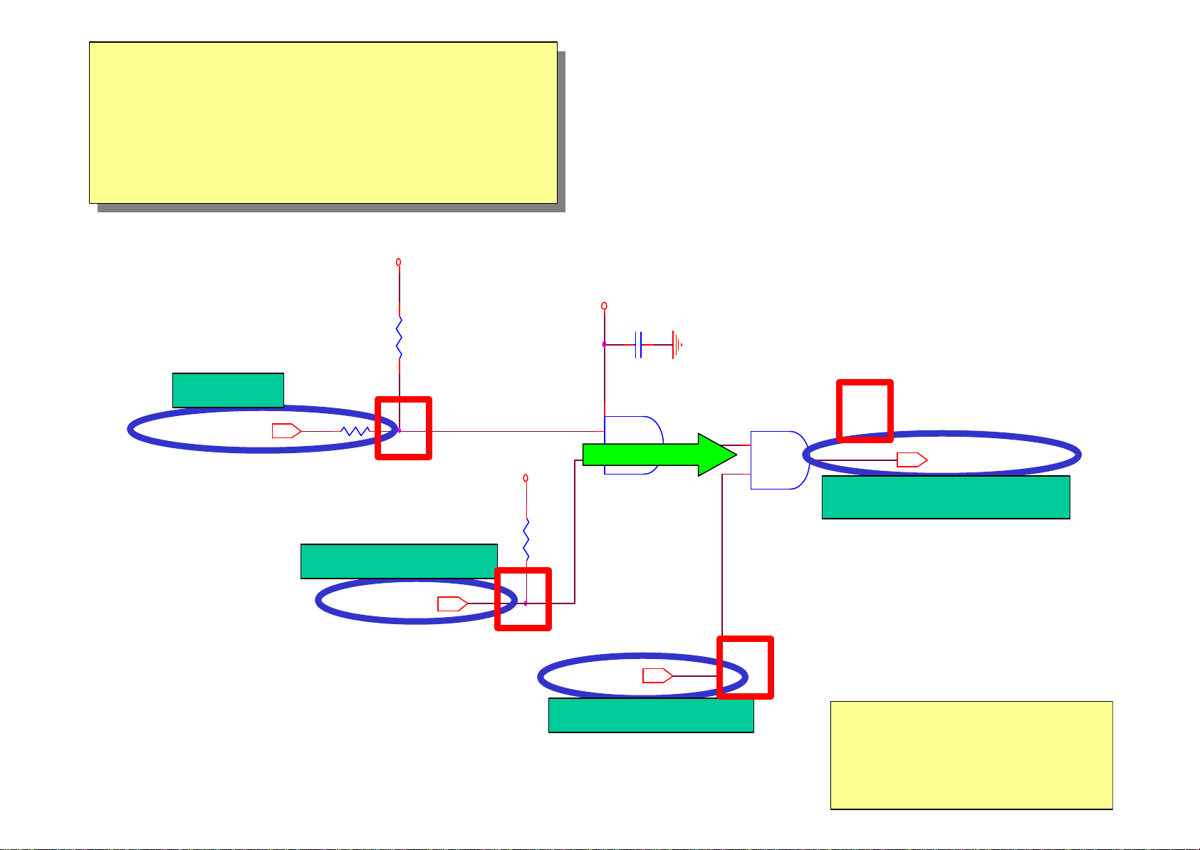
causes CK-408 active.
R389 0_NC
+3VSUS
C652
.047U
SLP_S1#_G
SLP_S3#
5
2
1
4
U37
7SH08
VTT_PWRGD#(P12)
SLP_S1# 12,14
VTT_PWRGD#38
PWR_DWN#
L
VTT_PWRGD#
RHU002N06
Binchuan:
Binchuan:
Then VTT_PWRGD# causes CK-408 pin-28 active to
Then VTT_PWRGD# causes CK-408 pin-28 active to
transmit All system clocks.(STP_PCI#,STP_CPU# can let
transmit All system clocks.(STP_PCI#,STP_CPU# can let
system stop its Clock .)
system stop its Clock .)
Binchuan:
Binchuan:
Q43
+3VRUN
R352
10K
31
2
STP_CLK# isn’t working, it ’s ignored
STP_CLK# isn’t working, it ’s ignored
by its inner register of BIOS controlling
by its inner register of BIOS controlling
from SMBus.
from SMBus.
R351
IMVP_PWRGD 5,9,35
10K
H
IMVP_PWRGD#
VTT_PWRGD#
L
STP_PCI#
STP_S1_G#
STP_CPU#
ICH4
CK-408
Page 24
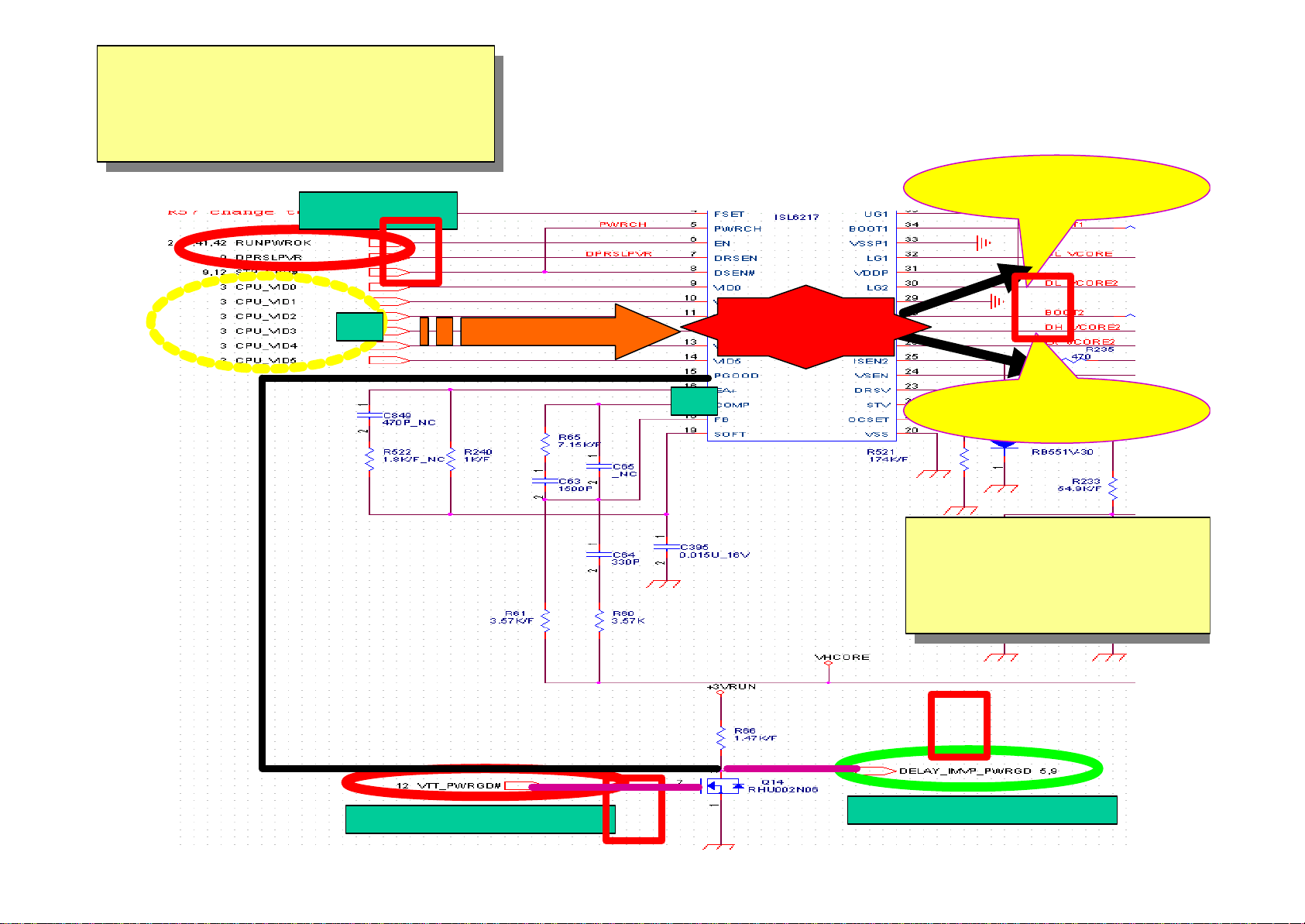
Binchuan:
Faces
Binchuan:
RUNPWROK ? VHCORE
RUNPWROK ? VHCORE
? DELAY_IMVP_PWRGD.
? DELAY_IMVP_PWRGD.
RUNPWROK
VID
H
VHCORE, DELAY_IMVP_PWRGD(P38)
VHCROE
H
ISL6217
PGOOD
VHCORE
Binchuan:
Binchuan:
VTT_PWRGD#
L
ISL6217 uses Two-Faces
ISL6217 uses Two-
of VHCORE POWER
of VHCORE POWER
H
DELAY_IMVP_PWRGD
Page 25

Binchuan:
Binchuan:
(H). DELAY_IMVP_PWRGD
(H). DELAY_IMVP_PWRGD
access into ICH4 will generate
access into ICH4 will generate
PCIRST#(Low? High) L?H
PCIRST#(Low? High) L?H
PCIRST#(P7,9)
ICH4
L?H
PCIRST#
PCIRST#
DELAY_IMVP_PWRGD
Transition
PWROK
H
ICH4
Page 26
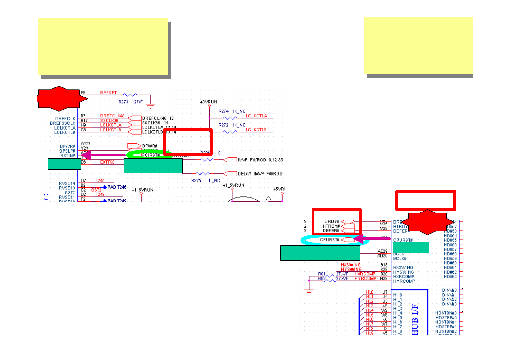
Binchuan:
Binchuan:
Binchuan:
Binchuan:
(I). PCIRST# access into
(I). PCIRST# access into
GMCH to generate
GMCH to generate
CPURST#.
CPURST#.
RSTIN#
PCIRST#
CPURST#(P4,5)
L?H
PCIRST# inactive will
PCIRST# inactive will
occur CPURST#
occur CPURST#
inactive.
inactive.
Transition
L?H
CPURST#
GMCH
CPURST#
Page 27
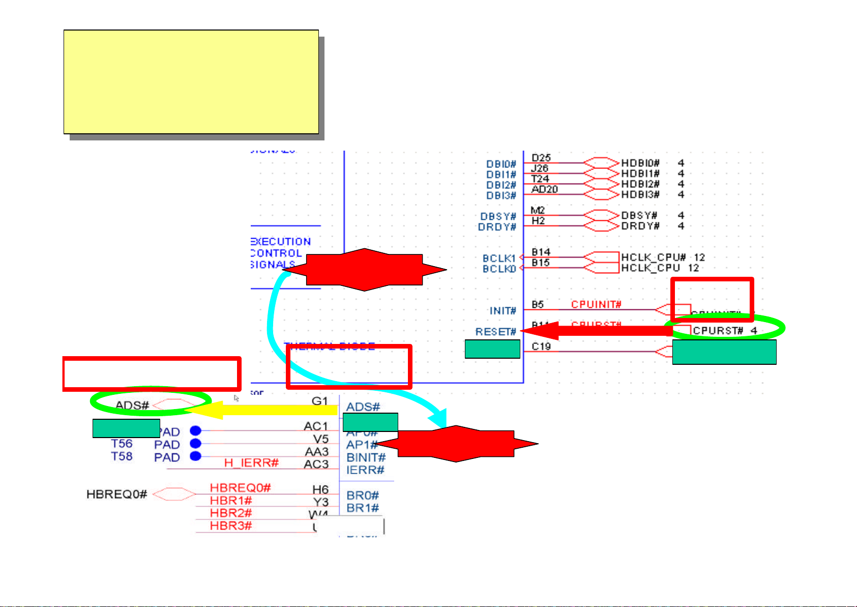
Binchuan:
Binchuan:
After CPURST# inactive, and all other
After CPURST# inactive, and all other
necessary signals are all to be
necessary signals are all to be
initiated from ICH -4 to CPUthat
initiated from ICH -4 to CPUthat
have correct configuration.
have correct configuration.
CENTRINO
ADS#, Miscellanea(P2)
L?H
… HHLL… .LHLHH..
ADS#
Transition
ADS#
RESET#
CENTRINO
CPURST#
Page 28

Binchuan:
Binchuan:
The Inner A0#~A2# value
The Inner A0#~A2# value
is 000.
is 000.
FFFFFFF0 point to BIOS
FFFFFFF0 point to BIOS
Entry-Point.
Entry-Point.
The address of Entry-Point(P2)
FFFFFFF0
Binchuan:
Binchuan:
AGTL+ ? HUBLINK? PCI/LPC to
AGTL+ ? HUBLINK? PCI/LPC to
point BIOS address of Entry
point BIOS address of Entry
address.
address.
0
1
1
1
1
1
1
1
1
1
1
1
1
1
1
1
1
1
1
1
1
1
1
1
1
1
1
1
1
CENTRINO
Page 29
Binchuan:
instructions to do its interpretation/ translation.
Binchuan:
FLASH need VCC1_PWROK#
FLASH need VCC1_PWROK#
to reset, and FLASH Control
to reset, and FLASH Control
Signal from MACALLEN(SIO).
Signal from MACALLEN(SIO).
Remainder action of Power
SIO_FA[0..19]
Transition
FCS#22
FRD#22
FWR#22
on(P25)
8Mbit (1M Byte),NO PLCC TYPE
SIO_FA0
SIO_FA1
SIO_FA2
SIO_FA3
SIO_FA4
SIO_FA5
SIO_FA6
SIO_FA7
SIO_FA8
SIO_FA9
SIO_FA10
SIO_FA11
SIO_FA12
SIO_FA13
SIO_FA14
SIO_FA15
SIO_FA16
SIO_FA17
SIO_FA18
SIO_FA19
FCS#
FRD#
FWR#
U6
21
A0
20
A1
19
A2
18
A3
17
A4
16
A5
15
A6
14
A7
8
A8
7
A9
36
A10
6
A11
5
A12
4
A13
3
A14
2
A15
1
A16
40
A17
13
A18
37
22
24
FLASH
A19
CE#
OE#
9
WE#
ST MICRO M29W008AB1/SST39VF080
D0
D1
D2
D3
D4
D5
D6
D7
RESET#
RESET#/NC
RY/BY#/NC
NC
NC
NC
VCC
VCC
GND
GND
25
26
27
28
32
33
34
35
10
12
29
38
11
31
30
23
39
SIO_FD0
SIO_FD1
SIO_FD2
SIO_FD3
SIO_FD4
SIO_FD5
SIO_FD6
SIO_FD7
+3VALW
C159
.1U
SIO_FD[0..7]
R101 0
T30 PAD
C158
.047U
Binchuan:
Binchuan:
VCC1_PWROK# inactive while
VCC1_PWROK# inactive while
+3VALW assert.
+3VALW assert.
SIO_FD[0..7] 22SIO_FA[0..19]22
L?H
VCC1_PWROK
12
VCC1_PWROK#
VCC1_PWROK 22
Binchuan:
Binchuan:
FLASH Control
FLASH Control
signals.
signals.
Binchuan:
Binchuan:
FLASH connect with MACALLEN(SIO) by
FLASH connect with MACALLEN(SIO) by
X-BUS. And SIO has some translated
X-BUS. And SIO has some translated
instructions to do its interpretation/ translation.
Page 30

Summary Sequence (1)
Test Purpose:
Overview of Procedure:
Timing Variable Time Comments
T1 280us
T2 -200us
T3 -184us
T4 170us
T5 -80us
T6 580us
T7 -454.2ms
T8 -3.744us
T9 520us
T10 -80us
T11 30us
T12 10us
T13 46.8ms
T14 -46ms
T15 -880us
T16 -80us
T17 860us
T18 780us
T19 420us
T20 157ms
To record the timing sequence for the power rails.
Measure the timing of the power rails. The definition of these timing variables is
given in the power sequencing document attached below this table.
Delay time form DC_IN+ to +RTCSRC
Delay time form +RTCSRC to +RTC_PWR5V
Delay time form +RTC_PWR5V to +RTC_PWR3_3V
Delay time form +RTC_PWR3_3V to +3VALW
Delay time form +3VALW to +5VALW
Delay time form +5VALW to POWER_SIO#
Delay time form POWER_SIO# to SUS_ON
Delay time form SUS_ON to AUXEN
Delay time form AUXEN to +3V_LAN
Delay time form +3V_LAN to 12OUT
Delay time form 12OUT to +5VSUS
Delay time form +5VSUS to +3V_SRC
Delay time form +3V_SRC to SUSPWROK_5V
Delay time form SUSPWROK_5V to +1.5VSUS
Delay time form +1.5VSUS to 3VSUS_ON
Delay time form 3VSUS_ON to +3VSUS
Delay time form +3VSUS to +2.5VSUS
Delay time form +2.5VSUS to SMDDR_VREF
Delay time form SMDDR_VREF to 2.5V_PWRGD
Delay time form 2.5V_PWRGD to LAN_PWROK
Page 31

Summary Sequence (2)
T21 -127ms
T22 98ms
T23 290us
T24 30us
T25 -57us
T26 110us
T27 256us
T28 1.372ms
T29 -1.728ms
T30 194us
T31 8.86ms
T32 15.12us
Delay time form LAN_PEROK to SUSPWROK
Delay time form SUSPWROK to RUN_ON
Delay time form RUN_ON to +2_5VRUN
Delay time form +2.5VRUN to +3VRUN
Delay time form +3VRUN to +1.5VRUN
Delay time form +1.5VRUN to +5VRUN
Delay time form +5VRUN to SMDDR_VTERM
Delay time form SMDDR_VTERM to
1.25V_PWRGD
Delay time form 1.25V_PWRGD to +1.8VRUN
Delay time form +1.8VRUN to
1715_1.5V_PWRGOOD
Delay time form 1715_1.5V_PWRGOOD to
RUNPWROK
Delay time form RUNPWROK to +12V
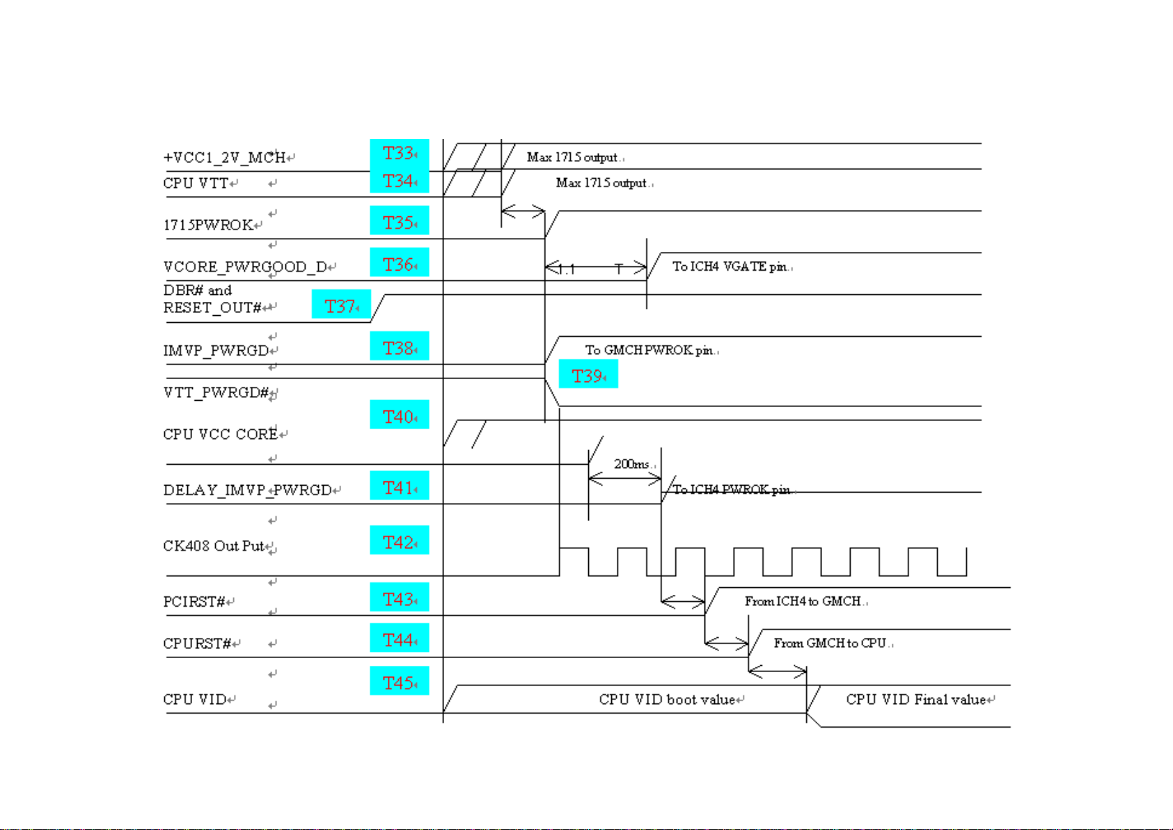
T33 940us
T34 -70us
T35 410us
T36 9.79ms
Delay time form +12V to +VCC1_2V_MCH
Delay time form +VCC1_2V_MCH to CPU VTT
Delay time form CPU VTT to 1715PWROK
Delay time form 1715PWROK to
VCORE_PWRGOOD_D
Page 32

Summary Sequence (3)
T37 9.2ms
T38 -10us
T39 -29.26ms
T40 9.16ms
T41 28.88ms
T42 -7.16ms
T43 8.32ms
T44 900us
T45 -28.86ms
Delay time form VCORE_PWRGOOD_D to DBR#
and RESET_OUT#
Delay time form DBR# and RESET_OUT# to
IMVP_PWRGD
Delay time form IMVP_PWRGD to VTT_PWRGD#
Delay time form VTT_PWRGD# to VHCORE
Delay time form CPU VCC CPRE to
DELAY_IMVP_PWRGD
Delay time form DELAY_IMVP_PWRGD to CK408
OUT PUT
Delay time form CK408 OUT PUT to PCIRST#
Delay time form PCIRST# to CPURST#
Delay time form CPURST# to CPU VID
Section Owner:
Section Tester:
Time To Complete:
Date Finished: Dec/05/2002
Page 33

The Procedure of Power-UP(1)
Page 34

The Procedure of Power-UP(2)
Page 35

The Procedure of Power
-
UP(3)
Page 36
The Procedure of Power-UP(4)
Page 37
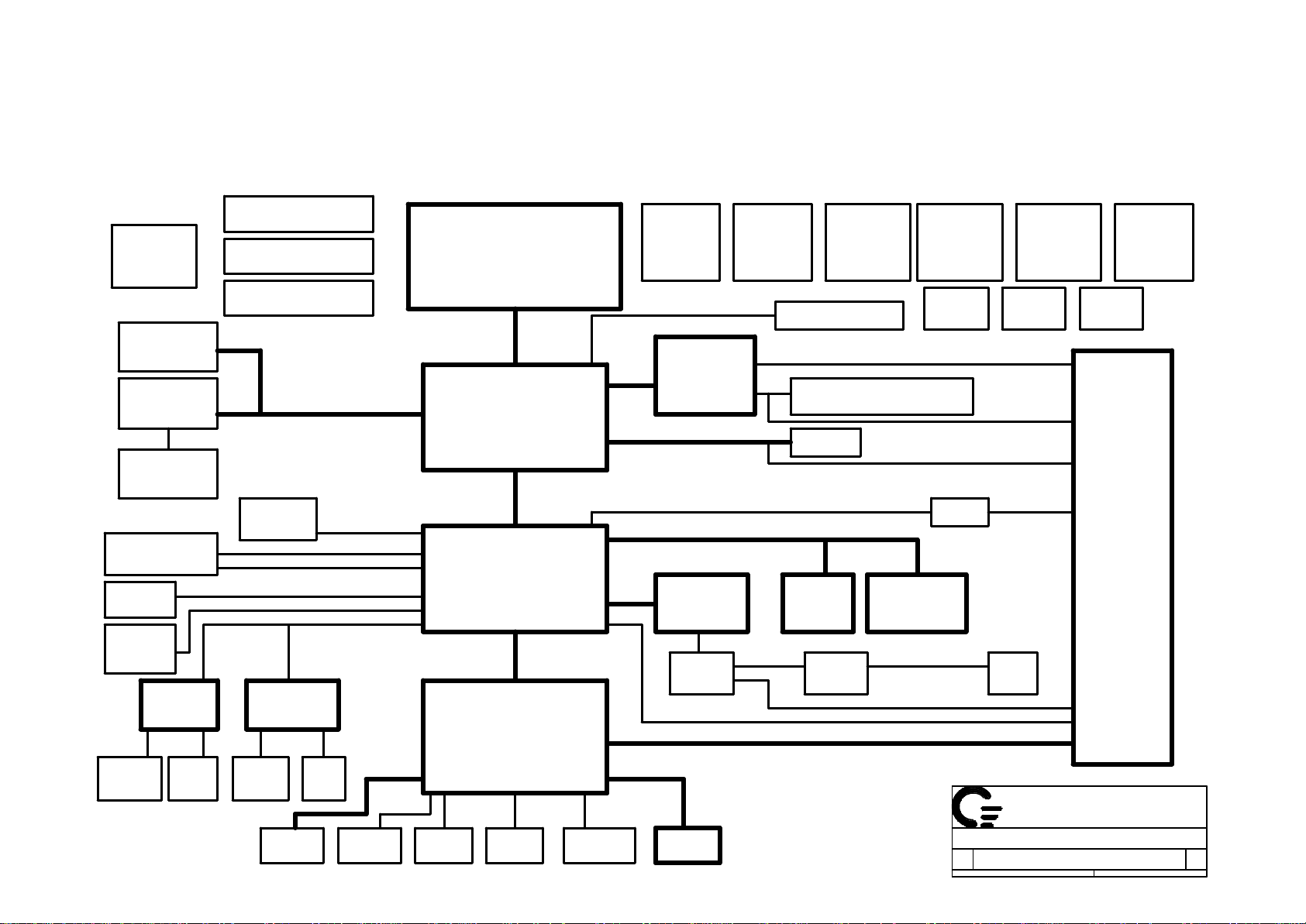
Appendix.
DAYTONA
RUN POWER
SW
PG 44
DDR-SODIMM1
PG 10
DDR-SODIMM2
PG 10
DDR-Termiation
PG 11
Internal Media Bay
CD-ROM
USB CONN.
PG 26
Blue Tooth
CONN.
PG 25
PG 16
AUDIO
PG 29,30
AC/BATT
CONNECTOR
BATT
SELECTOR
BATT
CHARGER
266/200 MHZ DDR
IDE1 - HDD
PG 16
USB
USB X2
USB
MDC
PG 20
PG 43
PG 36
PG 37
ATA 66/100
ATA 66/100
USB 2.0
AC97
Banias
(Micro-FCPGA)
PG 2,3
Montara-GM
MGM
732 Micro-FCBGA
PG 4,5,6
66(266)MHZ, 1.8V
HUB I/F
ICH4-M
421 BGA
PG 7,8,9
LPC
SIO(Macallen)
256 Pins LBGA
4X100MHZ
DVOB
DC/DC
PG 42
LVDS
Chrontel 7009
TV EN-CONDE
PG 13
PHY
PG 31
SWITCH
PG 31
USB
CPU VR
PG 38
Panel Connector
PG 14
33MHZ, 3.3V PCI
MINI-PCI
Wireless LAN
Bluetooth
Vtt &
VCC_1.2_MCH
PG 39 PG 41
DVI
S-Video
SEE I/O Board PG 1
VGA
PG 15
CARDBUS
PG 19
Magnetics
PG 32
OZ6912
DOCK LPC
1.5V,1.8V
2.5V,1.25V
FAN &
THERMAL
PG 28
1 Ports
USB
PG 18
PAD &
SCREW
PG 17
RJ45
PG 32
CLOCKS
PG 12
RESET CKT
PG 35
SWITCH &
LED
PG 27
DOCKING
CONNECTOR
PG 34
S/PDIF to
DOCK
PG 33
Audio
Jacks
PG 29
RJ11 to
DOCK
PG 33
IrDA
PG 3
Tip
Ring
PG 20
Keyboard
Parallel
PG 24
PG 21,22
Serial
PG 23PG 22
PS/2
Touchpad/
Stick point
PG 26
X-Bus
Flash
PG 25
QUANTA
Title
Size Document Number Rev
Date: Sheet of
COMPUTER
Schematic Block Diagram1
JM3 1A
星期二 二月
1 55, 11, 2003
 Loading...