

Page 1
Q-TECH
COR PORATI ON
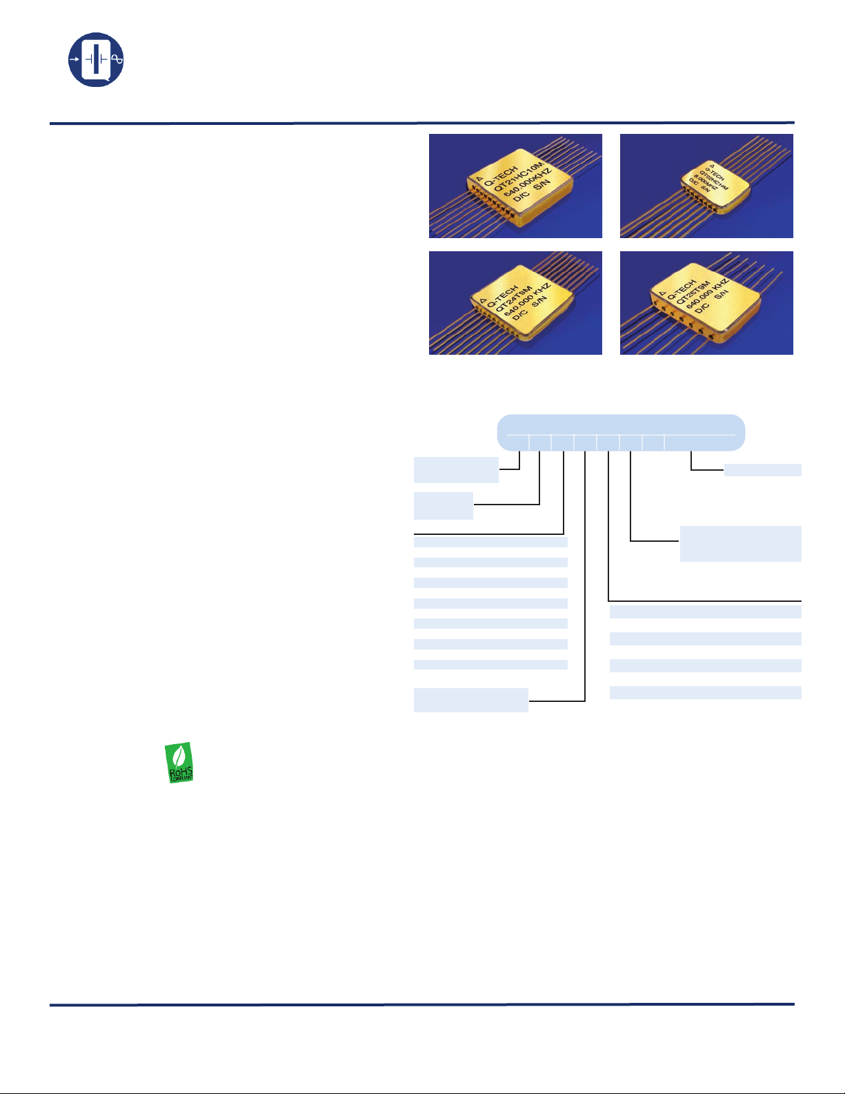
Description
Q-Tech’s flat pack crystal oscillators consist of a source
clock square wave generator, logic output buffers
and/or logic divider stages, and a round AT highprecision quartz crystal built in an all metal flat
package.
Features
• Made in the USA
• ECCN: EAR99
• DFARS 252-225-7014 Compliant:
Electronic Component Exemption
• USML Registration # M17677
• Wide frequency range from 0.12Hz to 200MHz
• Available as QPL MIL-PRF-55310/21 (TTL)
QT24 only
• Choice of flat packs and pin outs
• Choice of supply voltages
• Choice of output logic options
• AT-Cut crystal
• All metal hermetically sealed package
• Tight or custom symmetry available
• Capacitive load drive capability (Z output)
• Low height
• External tuning capacitor option
• Fundamental and third overtone designs
• Tristate function option D
• Three-point crystal mounts
• Custom design available tailors to meet
customer’s needs
• Q-Tech does not use pure lead or pure tin in its
products
• RoHS compliant
Applications
• Designed to meet today’s requirements for all
voltage applications
• Wide military clock applications
• Industrial controls
• Microcontroller driver
FLAT PACK
CRYSTAL CLOCK OSCILLATORS
-5.2 to -4.5Vdc & 1.8 to 15Vdc - 0.12Hz to 200MHz
Ordering Information
Sample part number
QT24ACD10M-2 0 . 0 0 0 MHz
QT 24 AC D 10 M-20.000MHz
T = Standard
S = Solder Dip (*)
Model #
(See page 3)
C = CMOS +5V to +15V (**)
AC = ACMOS +5V
HC = HCMOS +5V
T = TTL +5V
L = LVHCMOS +3.3V
N = LVHCMOS +2.5V
R = LVHCMOS +1.8V
E = 10K ECL -5.2V
EH = 10KH ECL -5.2V
EF = 100K/300K ECL -4.5V
PE = PECL +5V
LP = PECL +3.3V
Z = Z output
Tristate Option D
(Left blank if no Tristate)
(*) Hot Solder Dip Sn60 per MIL-PRF 55310 is optional for an additional cost
(**) Please specify supply voltage when ordering CMOS
For frequency stability vs. temperature options not listed herein, request a custom
part number.
For Non-Standard requirements, contact Q-Tech Corporation at
Sales@Q-Tech.com
1 = ± 100ppm at 0ºC to +70ºC
4 = ± 50ppm at 0ºC to +70ºC
5 = ± 25ppm at -20ºC to +70ºC
6 = ± 50ppm at -55ºC to +105ºC
9 = ± 50ppm at -55ºC to +125ºC
10 = ± 100ppm at -55ºC to +125ºC
11 = ± 50ppm at -40ºC to +85ºC
12 = ± 100ppm at -40ºC to +85ºC
Screened to
MIL-PRF-55310,level B
(Left blank if no screening)
Packaging Options
• Standard packaging in a locked anti-static cardboard
Other Options Available For An Additional Charge
• Lead forming available on all packages. Please contact for details.
• P. I. N. D. test (MIL-STD 883, Method 2020)
• Lead trimming
Output frequency
All Flat Pack packages are available in surface mount form.
Specifications subject to change without prior notice.
Q-TECH Corporation - 10150 W. Jefferson Boulevard, Culver City 90232 - Tel: 310-836-7900 - Fax: 310-836-2157 - www.q-tec h.com
Flat Pack (Revision F, August 2010 ) (ECO# 9934)
1
Page 2

Q-TECH
COR PORATI ON
Electrical Characteristics
FLAT PACK
CRYSTAL CLOCK OSCILLATORS
-5.2 to -4.5Vdc & 1.8 to 15Vdc - 0.12Hz to 200MHz
Parameters C AC HC
Output freq. range
(Fo)
Supply voltage (Vdd)
Maximum Applied Voltage (Vdd max.)
Freq. stability (∆F/∆T) See Option codes
Operating temp. (Topr) See Option codes
Storage temp. (Tsto) -62ºC to + 125ºC
Operating supply current
(Idd) (No Load)
Symmetry
(50% of ouput waveform or 1.4Vdc for
TTL)
Rise and Fall times
(with typical load)
Output Load
Start-up time (Tstup) 10ms max.
Output voltage (Voh/Vol)
Output Current (Ioh/Iol)
Enable/Disable
Tristate function
Jitter RMS 1σ (at 25ºC)
Aging (at 70ºC)
QT21, 24, 25
QT22, 26, 28
500Hz — 15MHz
500Hz — 15MHz 500Hz — 85MHz 500Hz — 85MHz 500Hz — 85MHz 500Hz — 85MHz
5V ~ 15Vdc ± 10% 5.0Vdc ± 10%
-0.5 to +18Vdc -0.5 to +7.0Vdc -0.5 to +5.0Vdc
F and Vdd dependent
3 mA max. at 5V up to 5MHz
25 mA max. at 15V up to 15MHz
45/55% max. Fo < 4MHz
40/60% max. Fo ≥ 4MHz
30ns max.
(Measured from 10% to 90%)
0.9 x Vdd min.; 0.1 x Vdd max. 2.4V min.; 0.4V max. 0.9 x Vdd min.; 0.1 x Vdd max. -1.15V min; -1.54V max. (E)
± 1mA typ. at 5V
± 6.8mA typ. at 15V
Call for details
500Hz — 125MHz
15pF // 10kΩ
± 24mA
8ps typ. - < 40MHz
5ps typ. - ≥ 40MHz
0.12Hz — 125MHz
20 mA max. - 0.12Hz ~ < 16MHz
25 mA max. - 16MHz ~ < 40MHz
35 mA max. - 40MHz ~ < 60MHz
45 mA max. - 60MHz ~ < 85MHz
60 mA max. - 85MHz ~ 125MHz
45/55% max. Fo < 12MHz
40/60% max. Fo ≥ 12MHz
15ns max. Fo < 15kHz
6ns max. Fo 15kHz ~ 39.999MHz
3ns max. Fo 40MHz ~ 160 MHz
(Measured from 10% to 90% CMOS or from 0.8V to 2.0V TTL)
±8 mA -1.6mA / TTL
VIH ≥ 2.2V Oscillation;
VIL ≤ 0.8V High Impedance
± 5ppm max. first year / ± 2ppm typ. per year thereafter
T L (*)
0.12Hz — 125MHz
10TTL Fo < 20MHz
6TTL Fo ≥ 20MHz
+40μA / TTL
0.12Hz — 160MHz
3.3Vdc ± 10%
3 mA max. - 0.12Hz ~ < 500kHz
6 mA max. - 500kHz ~ < 16MHz
10 mA max. - 16MHz ~ < 32MHz
20 mA max. - 32MHz ~ < 60MHz
30 mA max. - 60MHz ~ < 100MHz
40 mA max. - 100MHz ~ < 130MHz
50 mA max. - 130MHz ~ 160MHz
15pF // 10kΩ
± 4mA . -50mA
VIH ≥ 0.7 x Vdd Oscillation;
VIL ≤ 0.3 x Vdd High Impedance
15ps typ. - < 40MHz
8ps typ. - ≥ 40MHz
ECL / PECL (**)
1 MHz — 200MHz
8MHz — 85MHz
-5.2Vdc ± 5% (10K / 10KHECL)
5Vdc ± 5% (PECL)
3.3Vdc ± 5% (LVPECL)
0 to -8.0Vdc (10K / 10KHECL)
0 to +8.0Vdc (PECL)
0 to +5.0Vdc (LVPECL)
45 mA max. - 8MHz ~ < 125MHz
75 mA max. - 125MHz ~ 200MHz
45/55% max. Fo < 12MHz
40/60% max. Fo ≥ 12MHz
3.5ns max. Fo < 125MHz
3ns max. Fo 125MHz ~ 200MHz
(Measured from 20% to 80%)
50Ω to -2V (10K / 10KH)
50Ω to Vcc -2V (P & LP)
4V min.; 3.37V max. (PE)
2.27V min.; 1.68V max. (LP)
Call for details
Integrated phase jitter
12kHz - 20MHz 1ps typ.
(*) Available in 2.5Vdc (N) or 1.8Vdc (R)
(**) Please contact Q-Tech for details on 100KECL logic (EF)
Z Output logic can drive up to 200 pF load with typical 6ns rise & fall times (tr, tf)
Q-TECH Corporation - 10150 W. Jefferson Boulevard, Culver City 90232 - Tel: 310-836-7900 - Fax: 310-836-2157 - www.q-t ech.co m
Flat Pack (Revision F, August 2010 ) (ECO# 9934)
2
Page 3

Q-TECH
1
10 11
20
Q-TECH
P/N
FREQ.
(2.16/1.78)
.085/.070 .010
(.254)
(3.56)
.140
(15.88)
.625
(11.43)
.450
.050
(1.27)
(.381)
.015
SQ.
D/C S/N
.500
(12.70)
MIN.
.015
(.381)
(1.27)
.050
.450
(11.43)
.625
(15.88)
(.254)
.010.060/.045
(1.52/1.14)
(3.81)
.150
FREQ.
P/N
Q-TECH
20
1110
1
MAX.
SQ.
D/C S/N
.500
(12.70)
MIN.
1
78
14
FREQ.
P/N
Q-TECH
D/C S/N
.590
.790
.600
.500
.100
(2.54)
.015
(.381)
(12.70)
(20.07)
(15.24)
(14.99)
MIN.
.070
.160
(.254)
.010
(4.06)
MAX.
(1.78)
(.381)
.015
(9.53)
.375
(8.89)
.350
.010
.05
.15
1
89
16
Q-TECH
P/N
FREQ.
D/C S/N
(3.05)
.120
MAX.
.500
(12.70)
(1.27)
.050
(3.81)
MIN.
(.254)
(1.27)
.05
MIN.
(1.27)
1
89
16
(3.05)
.120
.060/.035
(1.52/.889)
.010
(.254)
(.381)
.015
.500
(12.70)
(1.27)
.050
(8.89)
.350
(9.53)
.375
MAX.
Q-TECH
P/N
FREQ.
D/C S/N
.500
(12.70)
MIN.
1
10 11
20
Q-TECH
P/N
FREQ.
.120
(3.05)
(1.52/1.14)
.060/.045 .010
(.254)
(15.88)
.625
(11.43)
.450
.050
(1.27)
(.381)
.015
MAX.
SQ.
D/C S/N
.500
(12.70)
MIN.
COR PORATI ON
Package Configuration Versus Pin Connections
FLAT PACK
CRYSTAL CLOCK OSCILLATORS
-5.2 to -4.5Vdc & 1.8 to 15Vdc - 0.12Hz to 200MHz
QT21
E
QT26
A
B
QT22
C
QT24
D
QT25
F
QT28
QT # Conf Vcc GND Case
Output
QT21 A 13 10 10 11 12 N/A
(*)
E/D
or
N/C
Equivalent
MIL-PRF-55310
Configuration
Flat Pack (Revision F, August 2010 ) (ECO# 9934)
Q-TECH Corporation - 10150 W. Jefferson Boulevard, Culver City 90232 - Tel: 310-836-7900 - Fax: 310-836-2157 - www.q-tec h.com
Dimensions are in inches (mm)
QT22 B 8 9 9 10 11 N/A
QT24 C 13 10 10 11 12 /21 = QT24T
QT25 D 13 10 10 11 12 N/A
QT26 E 14 7 7 8 6 N/A
QT28 F 8 9 9 10 11 N/A
(*) ECL / PECL complimentary output available on pin 12
(except QT22, 26, & 28) with a Q-Tech custom part number
Package Information
• Package material (Header and Leads): Kovar
• Lead finish: Gold Plated – 50µ ~ 80µ inches
Nickel Underplate – 100µ ~ 250µ inches
• Cover: Kovar, Gold Plated – 50µ ~ 100µ inches
Nickel Underplate – 70µ ~ 90µ inches
• Package to lid attachment: Seam weld
• Weight: 2.0g typ., 4.0g max.
3
Page 4

Q-TECH
Vdd
GND
0.1xVdd
0.9xVdd
VOH
VOL
TrTf
TH
T
0.5xVdd
SYMMETRY = x 100%
TH
T
Ts
Start-up box
Oscilloscope
DUT
Variable Ramp
54616B Agilent
TYPICAL SET-UP FOR START-UP TIME
-
-
Output
Ground
Vdd
Out
GND
0.1µF
15pF
E/D
Tristate Function
Power
supply
10k
mA
Vdc
+
+
+
(*)
or
0.01µF
(*) CL includes probe and jig capacitance
Typical test circuit for CMOS logic
0
5
10
15
20
25
30
35
40
45
0.5 2816 24 27 32 36 40 48 50 55 65 70 75 85 100 125 133 150 160
Freq(MHz)
Icc (mA)
TYPICAL SUPPLY CURRENT ICC (mA) AT 3.3Vdc & 5.0Vdc CMOS Logic NO LOAD
Icc 3.3V Icc 5V
POWER
SUPPLY
+
-
mA
0.1µF
Vdc
-
Vdd OUT
OUT
GND
Typical test circuit for TTL logic.
0.01µF
Rs
(*) CL inclides the loading effect of the oscilloscope probe.
E/D
C
L
+
+
-
RL
LOAD
6 TTL
10 TTL
CL(*)
12pF
20pF
RL
430Ω
270Ω
RS
10kΩ
6kΩ
or
Vdd
POWER
SUPPLY
+
-
mA
Vdc
+
-
GND OUT
OUT
Vee
Typical test circuit for ECL logic.
0.1µF
or
0.01µF
50Ω
-2Vdc
-4.5V
or
-5.2V
FREQUENCY STABILITY VERSUS TEMPERATURE QT24T- 48.000MHz
-50
-40
-30
-20
-10
0
10
20
30
40
50
-55 -50 -45 -40 -35 -30 -25 -20 -15 -10 -5 0510 15 20 25 30 35 40 45 50 55 60 65 70 75 80 85 90 95 100 105 110 115 120 125
Temperature (°C)
Frequency Stability (PPM)
2_5 3_5 4_5 5_5
COR PORATI ON
FLAT PACK
CRYSTAL CLOCK OSCILLATORS
-5.2 to -4.5Vdc & 1.8 to 15Vdc - 0.12Hz to 200MHz
Test Circuit
Output Waveform (Typical)
Startup Time
Supply Current
The Tristate function on pin 1 has a built-in pull-up resistor typical 50kΩ, so it
can be left floating or tied to Vdd without deteriorating the electrical performance.
Frequency vs. Temperature Curve
Q-TECH Corporation - 10150 W. Jefferson Boulevard, Culver City 90232 - Tel: 310-836-7900 - Fax: 310-836-2157 - www.q-tec h.com
Flat Pack (Revision F, August 2010 ) (ECO# 9934)
4
Page 5

Q-TECH
45º 45º
Hybrid Case
Substrate
Die
D/A epoxy
D/A epoxy
Heat
Die
R1
D/A epoxy
Substrate
D/A epoxy
Hybrid Case
R2 R3 R4 R5
JA JC CA
Die
T
T
T
C
A
J
CA
JC
COR PORATI ON
Thermal Characteristics
The heat transfer model in a hybrid package is described in
figure 1.
Heat spreading occurs when heat flows into a material layer of
increased cross-sectional area. It is adequate to assume that
spreading occurs at a 45° angle.
The total thermal resistance is calculated by summing the
thermal resistances of each material in the thermal path
between the device and hybrid case.
FLAT PACK
CRYSTAL CLOCK OSCILLATORS
-5.2 to -4.5Vdc & 1.8 to 15Vdc - 0.12Hz to 200MHz
RT = R1 + R2 + R3 + R4 + R5
(Figure 1)
The total thermal resistance RT (see figure 2) between the heat
source (die) to the hybrid case is the Theta Junction to Case
(Theta JC) in°C/W.
• Theta junction to case (Theta JC) for this product is 30°C/W.
• Theta case to ambient (Theta CA) for this part is 100°C/W.
• Theta Junction to ambient (Theta JA) is 130°C/W.
Maximum power dissipation PD for this package at 25°C is:
• PD(max) = (TJ (max) – TA)/Theta JA
• With TJ = 175°C (Maximum junction temperature of die)
• PD(max) = (175 – 25)/130 = 1.15W
(Figure 2)
Environmental Specifications
Q-Tech Standard Screening/QCI (MIL-PRF55310) is available for all of our Flat Packs. Q-Tech can also customize screening and test
procedures to meet your specific requirements. The Flat Packs are designed and processed to exceed the following test conditions:
Environmental Test Test Conditions
Temperature cycling MIL-STD-883, Method 1010, Cond. B
Constant acceleration MIL-STD-883, Method 2001, Cond. A, Y1
Seal: Fine and Gross Leak MIL-STD-883, Method 1014, Cond. A and C
Burn-in 160 hours, 125°C with load
Aging 30 days, 70°C, ± 1.5ppm max
Vibration sinusoidal MIL-STD-202, Method 204, Cond. D
Shock, non operating MIL-STD-202, Method 213, Cond. I
Thermal shock, non operating MIL-STD-202, Method 107, Cond. B
Ambient pressure, non operating MIL-STD-202, 105, Cond. C, 5 minutes dwell time minimum
Resistance to solder heat MIL-STD-202, Method 210, Cond. C
Moisture resistance MIL-STD-202, Method 106
Terminal strength MIL-STD-202, Method 211, Cond. C
Resistance to solvents MIL-STD-202, Method 215
Solderability MIL-STD-202, Method 208
ESD Classification MIL-STD-883, Method 3015, Class 1HBM 0 to 1,999V
Moisture Sensitivity Level J-STD-020, MSL=1
Q-TECH Corporation - 10150 W. Jefferson Boulevard, Culver City 90232 - Tel: 310-836-7900 - Fax: 310-836-2157 - www.q-tec h.com
Flat Pack (Revision F, August 2010 ) (ECO# 9934)
Please contact Q-Tech for higher shock requirements
5
Page 6

Q-TECH
COR PORATI ON
Period Jitter
As data rates increase, effects of jitter become critical with
its budgets tighter. Jitter is the deviation of a timing event
of a signal from its ideal position. Jitter is complex and
is composed of both random and deterministic jitter
components. Random jitter (RJ) is theoretically unbounded and Gaussian in distribution. Deterministic jitter
(DJ) is bounded and does not follow any predictable
distribution. DJ is also referred to as systematic jitter. A
technique to measure period jitter (RMS) one standard
deviation (1σ) and peak-to-peak jitter in time domain is
to use a high sampling rate (>8G samples/s) digitizing
oscilloscope. Figure shows an example of peak-to-peak
jitter and RMS jitter (1σ) of a QT24L-20MHz, at 3.3Vdc.
FLAT PACK
CRYSTAL CLOCK OSCILLATORS
-5.2 to -4.5Vdc & 1.8 to 15Vdc - 0.12Hz to 200MHz
Phase Noise and Phase Jitter Integration
RMS jitter (1σ): 5.75ps Peak-to-peak jitter: 60ps
Phase noise is measured in the frequency domain, and is expressed as a ratio of signal power to noise power measured in a 1Hz
bandwidth at an offset frequency from the carrier, e.g. 10Hz, 100Hz, 1kHz, 10kHz, 100kHz, etc. Phase noise measurement is made
with an Agilent E5052A Signal Source Analyzer (SSA) with built-in outstanding low-noise DC power supply source. The DC source
is floated from the ground and isolated from external noise to ensure accuracy and repeatability.
In order to determine the total noise power over a certain frequency range (bandwidth), the time domain must be analyzed in the
frequency domain, and then reconstructed in the time domain into an rms value with the unwanted frequencies excluded. This may be
done by converting L(f) back to Sφ(f) over the bandwidth of interest, integrating and performing some calculations.
Symbol
∫L(f)
Sφ (f)=(180/Π)x√2 ∫L(f)df
RMS jitter = Sφ (f)/(fosc.360°) Jitter(in seconds) due to phase noise. Note Sφ (f) in degrees.
Integrated single side band phase noise (dBc)
Spectral density of phase modulation, also known as RMS phase error (in degrees)
Definition
The value of RMS jitter over the bandwidth of interest, e.g. 10kHz to 20MHz, 10Hz to 20MHz, represents 1 standard deviation of
phase jitter contributed by the noise in that defined bandwidth.
Figure below shows a typical Phase Noise/Phase jitter of a QT24HC, 5.0Vdc, 24MHz and QT24L, 3.3Vdc, 24MHz clock at offset frequencies 10Hz to 5MHz, and phase jitter integrated over the bandwidth of 12kHz to 1MHz.
QT24HC, 5.0Vdc, 24MHz
Q-TECH Corporation - 10150 W. Jefferson Boulevard, Culver City 90232 - Tel: 310-836-7900 - Fax: 310-836-2157 - www.q-tec h.com
Flat Pack (Revision F, August 2010 ) (ECO# 9934)
QT24L, 3.3Vdc, 24 MHz
6
 Loading...