

Page 1
Q-TECH
325 4
6 7 8 9 10
.500
(13.46)
.250
(6.35)
.030
(0.76)
.750
(19.06)
1.000
(25.40)
.750
(19.06)
1
.250
(6.35)
.500
(12.70)
1.000
(25.40)
.025
(.65)
Stand off
4 places
max
Sq.
Q-TECH
QT2010
75.000MHz
D/C S/N
COR PORATI ON
Description
Q-Tech’s microcomputer compensated crystal oscillator,
MCXO, uses a high stability overtone SC-cut crystal with microprocessor controlled compensation. The self-temperature
sensing resonator, using a dual-mode oscillator, virtually
eliminates thermometry related errors. As a result, all basic
TCXO and OCXO limitations are overcome or significantly
reduced in the MCXO.
Features
• Made in the USA
• ITAR
• DFARS 252-225-7014 Compliant:
Electronic Component Exemption
• USML Registration # M17677
• Frequency Stability-Temperature: ±2 x 10⁻⁸from
-40ºC to +85ºC (Extended temperature range available)
• Outputs: 5 to 100MHz, 32.768kHz and 1PPS.Other
frequency options available
• DC Power Input: 3.3Vdc, 105milliwatts max
• Inputs: Mode Control
Calibration Reference Signal
Sync (optional)
• Initialization: <5 seconds from power on to full
performance
• Dual-Mode Oscillator: Specially developed for the
MCXO
• Aging Correction: Auto calibration in the field
• Environmental: Inherently rugged design capable of
full military screening
• Low Phase Noise and Jitter
• Small Form Factor
• G-Sensitivity 1PPB/G max.
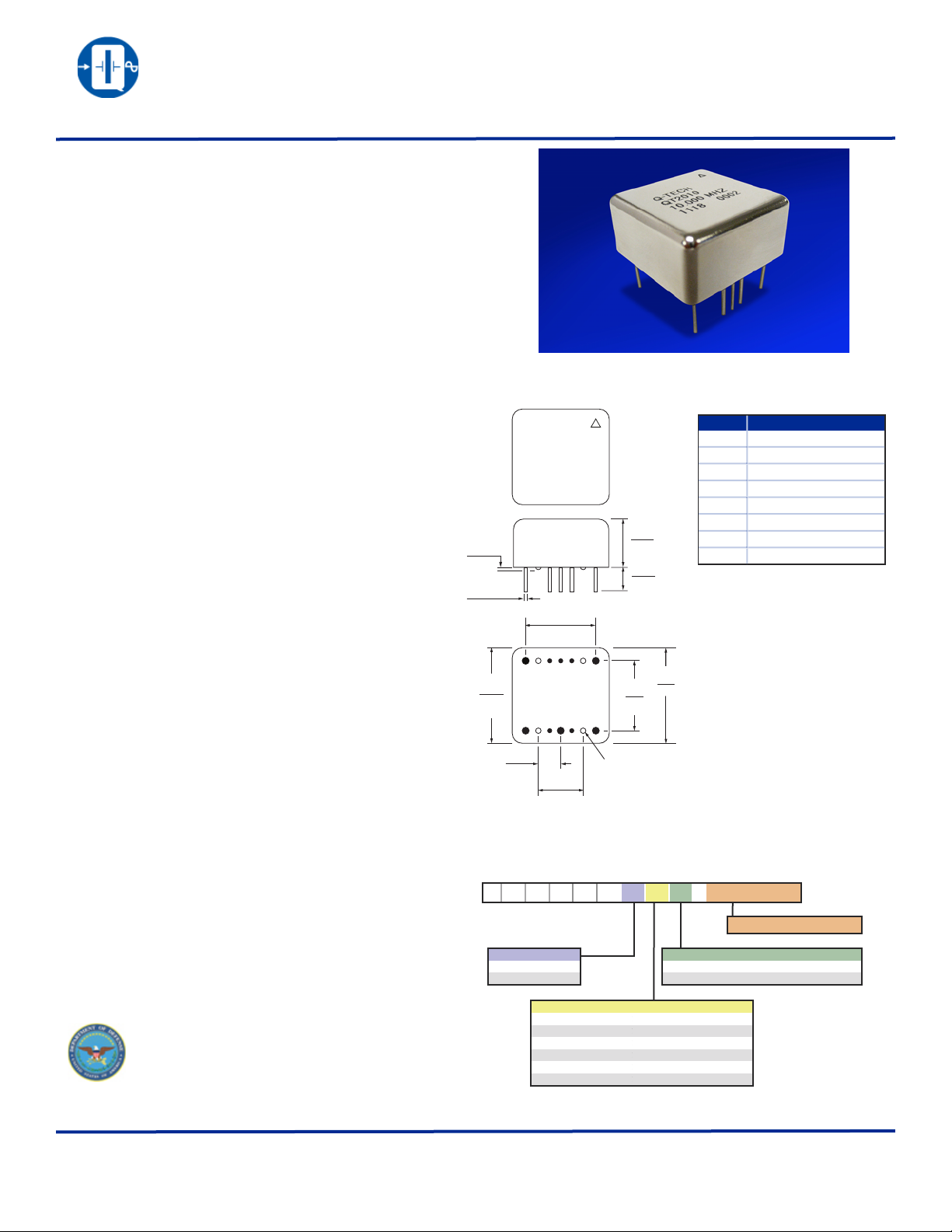
QT2010 MCXO
MICROCOMPUTER COMPENSATED CRYSTAL OSCILLATOR
3.3Vdc - 5 to 100MHz, 32.768kHz and 1PPS
Package Outline and Pin Connections
Dimensions are in inches (mm)
Pin No.
1
2, 4, 7
3
5
6
8
9
10
Package Material:
• .025 + .002/-.003
Cold Rolled Steel
• Bright Nickel Plated
500µ Solderable
Function
Frequency Output
N/C
GND / CASE
Vc/Fref Input
1PPS Output
Mode Select
Status
Voltage Supply
Applications
• Satellite terminals
• Underwater monitors
• GPS
• Mobile equipment
Q-T ECH Co rpo rat ion - 1 015 0 W. J efferson Boulevard, Culver City 90232 - Tel: 310-836-7900 - Fax: 310-836-2157 - www.q-t e c h.c om
QPDS-0004 (Revision B, October 2012 ) (ECO# 10690)
ITAR Controlled
Ordering Information
(Sample part number)
QT201 0 C B M - 1 0 . 0 0 0 M Hz
Q T 2 0 1 0 C B M- 10.000MHz
Output Frequency
Logic:
C = CMOS
S = Sine Wave
Frequency vs. Temperature Code:
A = ± 5ppb at 0ºC to +50ºC
B = ± 10ppb at 0ºC to +70ºC
C = ± 30ppb at -40ºC to +85ºC
D = ± 20ppb at -40ºC to +85ºC
E = ± 30ppb at -55ºC to +105ºC
F = ± 20ppb at -55ºC to +105ºC
For Non-Standard requirements, contact Q-Tech Corporation at
Blank = No Screening
Sales@Q-Tech.com
Screening Option:
M = Per MIL-PRF-55310, Level B
1 of 3
Page 2
QT2010 MCXO
Q-TECH
COR PORATI ON
Pinout Description
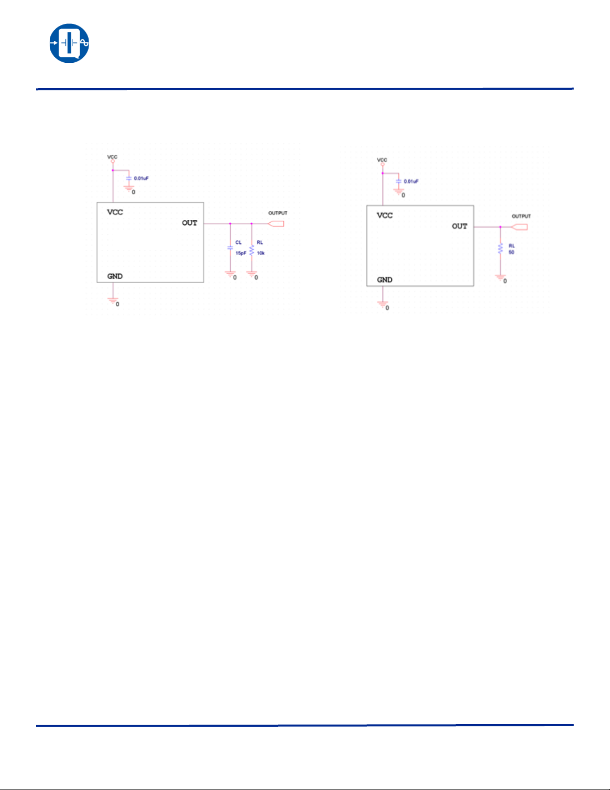
Pin #1 Frequency output. Depends on specification part number, Frequency output can be HCMOS or Sine Wave. HCMOS output
has 10 kOhm in parallel with 15pF load. Sine Wave output has 50 Ohm load.
MICROCOMPUTER COMPENSATED CRYSTAL OSCILLATOR
3.3Vdc - 5 to 100MHz, 32.768kHz and 1PPS
QT2010C
Frequency Output range is 5MHz to 100MHz.
Pin #3: Case Ground. This pin provides negative voltage (0V) to the MCXO. It is connected to the oscillator case to reduce EMI.
Pin #5: Vc/Reference Input. This input can be configured as Voltage Control or Reference. The configuration is one time
programming at the factory according to customer request. In case of Voltage Control setup, by providing voltage within range
of 0 to +3.3V output Frequency on the both Frequency and timing outputs will be changed within range of +/-2.5PPM. Vc
slope is positive. To get nominal frequency 1.65V on this input has to be applied. This function is used to compensate MCXO
aging. In case of Reference Input setup, 10MHz signal should be applied to the input. When 10MHz signal (1V p-p min) is
provided to the pin, MCXO starts aging correction routine and synchronizes both frequency and timing mode outputs to the
reference signal. The routine takes about 10-15 seconds. After frequency is synchronized MCXO continues to operate as
normal. In order to perform synchronization again, the reference should be disconnected and connected one more time.
Precision of synchronization is +/-5PPB.
Pin #6: 1PPS Output. This output provides 1PPS (1Hz) HCMOS signal. It also can be configured to provide 32.768 kHz HCMOS
signal. The configuration is one time programming at the factory according to customer request.
QT2010S
Pin #8: Mode Select. This pin is responsible for MCXO operating modes. If low level (<0.5v) signal is applied to the pin, MCXO
will start to operate in Frequency Mode. It will output signal with specified frequency at the pin#1. Pin#6 will be disabled.
Power consumption will be according to Frequency Mode specification. If high level (>2.8V) signal is applied to the pin,
MCXO will start to operate in Timing Mode. It will output 1PPS or 32.768 kHz signal at Pin#6. Power consumption will be
according to Timing Mode specification. Pin#1 will be disabled.
Pin #9: Status. Status output has low level signal during normal operation. It provides low frequency signal (2-4Hz) for 5-10 seconds
after power is applied to Pin#10. It goes high during aging correction routine. It also goes high in case of MCXO malfunction.
It can be connected to LED to indicate MCXO status.
Pin #10: Voltage Supply. This pin provides positive voltage (3.3V) to the MCXO. Minimum value of bypass capacitor is 2.2uF. It has
to be installed close pin#10.
Pins #2,4,7: Not Connected. Leave these pins not connected. They have internal functions and grounding them may lead to MCXO
malfunction.
Contact factory for deviations from the standard functions and operation.
Q-T ECH Co rpo rat ion - 1 015 0 W. J efferson Boulevard, Culver City 90232 - Tel: 310-836-7900 - Fax: 310-836-2157 - www.q-t e c h.c om
QPDS-0004 (Revision B, October 2012 ) (ECO# 10690)
2 of 3
Page 3

Q-TECH
Pararmeters
Symbol
Conditions Value Unit
Frequency Mode Parameters
Frequency Range fo -
5.000-100.000
MHz
Supply voltage, Nom. Vs Vs±5%
3.3
V
Power Consumption, max. Ps
Vs, nom. / Ta=+25°C (No load)
105
mW
Nominal Tolerance Fnom
Vs, nom. / Ta=+25°C
±10
ppb
Freq. Stability vs. Temperature
Δf/fc
(Ta)
Ta=-40°C…+85°C
±20
ppb
Freq. Stability vs. Load
Variation
Δfl
NpF
±5% Load Change
±20
ppb
Freq. Stability vs. Voltage
Supply Variation
Δfv ±5% Input Voltage Change
±20
ppb
Aging (Max)
HCMOS SINE WAVE
HCMOS SINE WAVE
Δ
f/fo
Per Day
Over 10 Years
Over 20 Years
±1.0
±1.0
±1.5
ppb
ppm
ppm
Output Waveform
3.3V 3dBm±3dBm
Symmetry
Ta=-40°C…+85°C
50±5
%
Rise/Fall Time (Max)
Ta=-40°C…+85°C
3
nSec
Startup Time (Max)
Ta=-40°C…+85°C, to ±50.0 ppm
20
mSec
Stabilization Time (Max)
Ta=-40°C…+85°C, to ±0.03 ppm
3
Sec
Phase Noise (10MHz)
10Hz
-110
dBc/Hz
100Hz
-135
dBc/Hz
1kHz
-145
dBc/Hz
10kHz
-155
dBc/Hz
100kHz
-160
dBc/Hz
Spurious (Max)
Ta=-40°C…+85°C, >1kHz offset
-100
dBc
Phase Noise Jitter
1kHz to 20MHz pSec
Aging Adjustment (10MHz ref)
Ta=+25° C, stable environment
±0.02
ppm
Timekeeping Mode Parameters
Frequency Nom.
Ft
Ta=-40°C…+85°C
1
1
PPS
Power Consumption, max. Ps
Vs, nom. / Ta=+25°C (No load)
90
mW
Freq. Stability vs. Temperature
Δf/Ft
(Ta)
Ta=-40°C…+85°C
±20
ppb
Output Waveform
HCMOS 3.3V
Symmetry
Ta=-40°C…+85°C
50±5
%
Rise/Fall Time (Max)
Ta=-40°C…+85°C
100
nSec
Startup Time (Max)
Ta=-40°C…+85°C ,to ±120.0 ppm
500
mSec
Stabilization Time (Max)
Ta=-40°C…+85°C, to ±0.03 ppm
3
Sec
Period Jitter
5
nSec
COR PORATI ON
Electrical Characteristics
QT2010 MCXO
MICROCOMPUTER COMPENSATED CRYSTAL OSCILLATOR
3.3Vdc - 5 to 100MHz, 32.768kHz and 1PPS
ECO REV REVISION SUMMARY Page
10690
Q-T ECH Co rpo rat ion - 1 015 0 W. J efferson Boulevard, Culver City 90232 - Tel: 310-836-7900 - Fax: 310-836-2157 - www.q-t e c h.c om
ADD PIN OUT DESCRIPTION 2
B
Add document number on footer of all pages All
QPDS-0004 (Revision B, October 2012 ) (ECO# 10690)
Revision History
3 of 3
 Loading...