


FEATURES
• Very high speed-10 MBit/s
• Superior CMR-10 kV/µs
• Double working voltage-480V
• Fan-out of 8 over -40°C to +85°C
• Logic gate output
• Strobable output
• Wired OR-open collector
• U.L. recognized (File # E90700)
DESCRIPTION
The 6N137, HCPL-2601/2611 single-channel and HCPL-2630/2631 dual-channel
optocouplers consist of a 850 nm AlGaAS LED, optically coupled to a very high
speed integrated photodetector logic gate with a strobable output. This output
features an open collector, thereby permitting wired OR outputs. The coupled
parameters are guaranteed over the temperature range of -40°C to +85°C. A
maximum input signal of 5 mA will provide a minimum output sink current of 13
mA (fan out of 8).
An internal noise shield provides superior common mode rejection of typically 10
kV/µs. The HCPL- 2601 and HCPL- 2631 has a minimum CMR of 5 kV/µs.
The HCPL-2611 has a minimum CMR of 10 kV/µs.
APPLICATIONS
• Ground loop elimination
• LSTTL to TTL, LSTTL or 5-volt CMOS
• Line receiver, data transmission
• Data multiplexing
• Switching power supplies
• Pulse transformer replacement
• Computer-peripheral interface
Input Enable Output
HHL
LHH
HLH
LLH
HNCL
LNCH
A 0.1
µF bypass capacitor must be connected between pins 8 and 5.
(See note 1)
TRUTH TABLE
(Positive Logic)
8/10/99 200002A
Dual-channel
circuit drawing
Single-channel
circuit drawing
HIGH SPEED-10 MBit/s
LOGIC GATE OPTOCOUPLERS
SINGLE-CHANNEL DUAL-CHANNEL
6N137 HCPL-2630
HCPL-2601 HCPL-2631
HCPL-2611
N/C
1
+
2
V
F
_
3
N/C
4 5
8
1
8
1
V
8
CC
V
7
E
V
6
O
GND
8
+
1
V
F1
_
2
_
3
V
F2
+
4 5
1
V
8
CC
V
7
01
V
6
02
GND
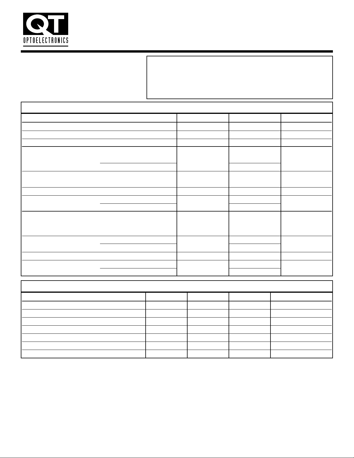
RECOMMENDED OPERATING CONDITIONS
Parameter Symbol Min Max Units
Input Current, Low Level I
FL
0 250 µA
Input Current, High Level I
FH
*6.3 15 mA
Supply Voltage, Output V
CC
4.5 5.5 V
Enable Voltage, Low Level V
EL
0 0.8 V
Enable Voltage, High Level V
EH
2.0 V
CC
V
Low Level Supply Current T
A
-40 +85 °C
Fan Out (TTL load) N 8
Parameter Symbol Value Units
Storage Temperature T
STG
-55 to +125 °C
Operating Temperature T
OPR
-40 to +85 °C
Lead Solder Temperature T
SOL
260 for 10 sec °C
EMITTER
DC/Average Forward Single channel I
F
50
mA
Input Current Dual channel (Each channel) 30
Enable Input Voltage Single channel
V
E
5.5 V
Not to exceed V
CC
by more than 500 mV
Reverse Input Voltage Each channel V
R
5.0 V
Power Dissipation Single channel
P
I
100
mW
Dual channel (Each channel) 45
DETECTOR
Supply Voltage
V
CC
7.0 V
(1 minute max)
Output Current Single channel
I
O
50
mA
Dual channel (Each channel) 50
Output Voltage Each channel V
O
7.0 V
Collector Output Single channel
P
O
85
mW
Power Dissipation Dual channel (Each channel) 60
ABSOLUTE MAXIMUM RATINGS (No derating required up to 85°C)
* 6.3 mA is a guard banded value which allows for at least 20 % CTR degradation. Initial input current threshold value is 5.0 mA or less
SINGLE-CHANNEL DUAL-CHANNEL
6N137 HCPL-2630
HCPL-2601 HCPL-2631
HCPL-2611
HIGH SPEED-10 MBit/s
LOGIC GATE OPTOCOUPLERS
8/10/99 200002A
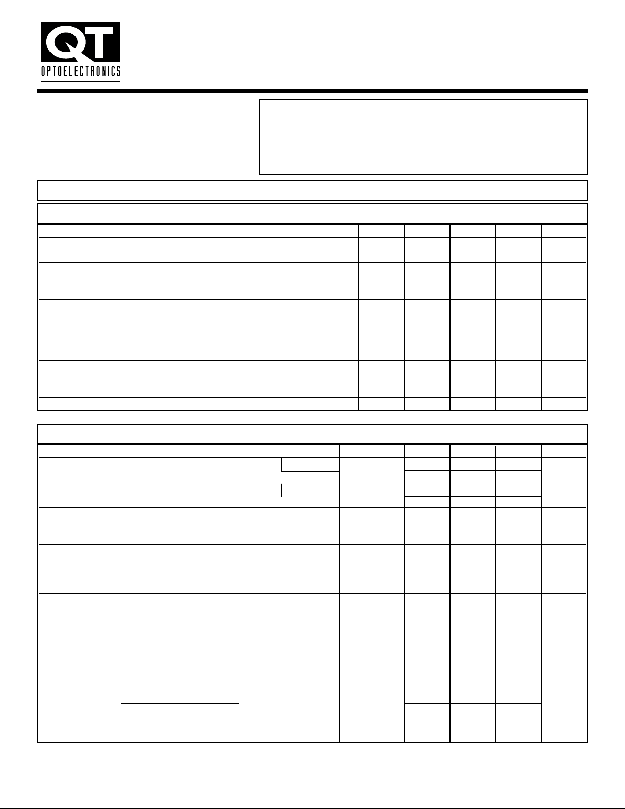
AC Characteristics Test Conditions Symbol Min Typ** Max Unit
Propagation Delay Time (Note 4) (TA=25°C)
T
PLH
20 45 75
ns
to Output High Level (R
L
= 350 !, CL= 15 pF) (Fig. 12) 100
Propagation Delay Time (Note 5) (TA=25°C)
T
PHL
25 45 75
ns
to Output Low Level (R
L
= 350 !, CL= 15 pF) (Fig. 12) 100
Pulse Width Distortion (RL= 350 !, CL= 15 pF) (Fig. 12) "T
PHL-TPLH
" 335ns
Output Rise Time (10-90%)
(R
L
= 350 !, CL= 15 pF)
t
r
50 ns
(Note 6) (Fig. 12)
Output Fall Time (90-10%)
(R
L
= 350 !, CL= 15 pF)
t
f
12 ns
(Note 7) (Fig. 12)
Enable Propagation Delay Time (IF= 7.5 mA, VEH= 3.5 V)
t
ELH
20 ns
to Output High Level (RL= 350 !, CL= 15 pF) (Note 8) (Fig. 13)
Enable Propagation Delay Time (IF= 7.5 mA, VEH= 3.5 V)
t
EHL
20 ns
to Output Low Level (RL= 350 !, CL= 15 pF) (Note 9) (Fig. 13)
Common Mode Transient Immunity (TA=25°C) "VCM" = 50 V, (Peak)
(at Output High Level) (I
F
= 0 mA, VOH(Min.) = 2.0 V)
"CM
H
" V/µs
6N137, HCPL-2630 (RL= 350 !) (Note 10) 10,000
HCPL-2601, HCPL-2631 (Fig. 14) 5000 10,000
HCPL-2611 "VCM" = 400 V 10,000 15,000
(RL= 350 !) (IF= 7.5 mA, VOL(Max.) = 0.8 V)
10,000
Common Mode 6N137, HCPL-2630 "V
CM
" = 50 V (Peak)
"CM
L
" V/µs
Transient Immunity HCPL-2601, HCPL-2631 (T
A
=25°C)
5000 10,000
(at Output Low Level) (Note 11) (Fig. 14)
HCPL-2611 (TA=25°C) "VCM" = 400 V 10,000 15,000
SWITCHING CHARACTERISTICS
(TA= -40°C to +85°C, V
CC
= 5 V, IF= 7.5 mA Unless otherwise specified.)
Parameter Test Conditions Symbol Min Typ** Max Unit
EMITTER (IF= 10 mA)
V
F
1.8
V
Input Forward Voltage T
A
=25°C 1.4 1.75
Input Reverse Breakdown Voltage (IR= 10 µA) B
VR
5.0 V
Input Capacitance (VF= 0, f = 1 MHz) C
IN
60 pF
Input Diode Temperature Coefficient (IF= 10 mA) #VF/#T
A
-1.4 mV/°C
DETECTOR
710
High Level Supply Current Single Channel (V
CC
= 5.5 V, IF= 0 mA) I
CCH
mA
Dual Channel (V
E
= 0.5 V) 15 20
Low Level Supply Current Single Channel (VCC= 5.5 V, IF= 10 mA)
I
CCL
913
mA
Dual Channel (V
E
= 0.5 V) 19 26
Low Level Enable Current (VCC= 5.5 V, VE= 0.5 V) I
EL
-0.8 -1.6 mA
High Level Enable Current (VCC= 5.5 V, VE= 2.0 V) I
EH
-0.6 -1.6 mA
High Level Enable Voltage (VCC= 5.5 V, IF= 10 mA) V
EH
2.0 V
Low Level Enable Voltage (VCC= 5.5 V, IF= 10 mA) (Note 3) V
EL
0.8 V
INDIVIDUAL COMPONENT CHARACTERISTICS
ELECTRICAL CHARACTERISTICS (T
A
= -40°Cto +85°C Unless otherwise specified.)
SINGLE-CHANNEL DUAL-CHANNEL
6N137 HCPL-2630
HCPL-2601 HCPL-2631
HCPL-2611
HIGH SPEED-10 MBit/s
LOGIC GATE OPTOCOUPLERS
8/10/99 200002A

Characteristics Test Conditions Symbol Min Typ** Max Unit
Input-Output (Relative humidity = 45%)
Insulation Leakage Current (T
A
= 25°C, t = 5 s)
I
I-O
1.0* µA
(V
I-O
= 3000 VDC)
(Note 12)
Withstand Insulation Test Voltage (RH < 50%, TA = 25°C)
V
ISO
2500 V
RMS
(Note 12) ( t = 1 min.)
Resistance (Input to Output) (V
I-O
= 500 V) (Note 12) R
I-O
10
12
!
Capacitance (Input to Output) (f = 1 MHz) (Note 12) C
I-O
0.6 pF
ISOLATION CHARACTERISTICS (T
A
= -40°C to +85°C Unless otherwise specified.)
** All typical values are at VCC= 5 V, TA= 25°C
1. The VCCsupply to each optoisolator must be bypassed by a 0.1µF capacitor or larger. This can be either a ceramic or solid tantalum
capacitor with good high frequency characteristic and should be connected as close as possible to the package V
CC
and GND pins
of each device.
2. Each channel.
3. Enable Input - No pull up resistor required as the device has an internal pull up resistor.
4. t
PLH
- Propagation delay is measured from the 3.75 mA level on the HIGH to LOW transition of the input current pulse to the 1.5 V
level on the LOW to HIGH transition of the output voltage pulse.
5. t
PHL
- Propagation delay is measured from the 3.75 mA level on the LOW to HIGH transition of the input current pulse to the 1.5 V
level on the HIGH to LOW transition of the output voltage pulse.
6. t
r
- Rise time is measured from the 90% to the 10% levels on the LOW to HIGH transition of the output pulse.
7. t
f
- Fall time is measured from the 10% to the 90% levels on the HIGH to LOW transition of the output pulse.
8. t
ELH
- Enable input propagation delay is measured from the 1.5 V level on the HIGH to LOW transition of the input voltage pulse
to the 1.5 V level on the LOW to HIGH transition of the output voltage pulse.
9. t
EHL
- Enable input propagation delay is measured from the 1.5 V level on the LOW to HIGH transition of the input voltage pulse
to the 1.5 V level on the HIGH to LOW transition of the output voltage pulse.
10. CMH - The maximum tolerable rate of rise of the common mode voltage to ensure the output will remain in the high state
(i.e., V
OUT
> 2.0 V). Measured in volts per microsecond (V/µs).
11. CM
L
- The maximum tolerable rate of rise of the common mode voltage to ensure the output will remain in the low output state
(i.e., V
OUT
< 0.8 V). Measured in volts per microsecond (V/µs).
12. Device considered a two-terminal device: Pins 1,2,3 and 4 shorted together, and Pins 5,6,7 and 8 shorted together.
NOTES
DC Characteristics Test Conditions Symbol Min Typ** Max Unit
High Level Output Current (VCC= 5.5 V, VO= 5.5 V)
I
OH
100 µA
(I
F
= 250 µA, VE= 2.0 V) (Note 2)
Low Level Output Current (VCC= 5.5 V, IF= 5 mA)
V
OL
.35 .06 V
(V
E
= 2.0 V, ICL= 13 mA) (Note 2)
Input Threshold Current
(V
CC
= 5.5 V, VO= 0.6 V,
I
FT
35mA
V
E
= 2.0 V, IOL= 13 mA)
TRANSFER CHARACTERISTICS
(TA= -40°C to +85°C Unless otherwise specified.)
SINGLE-CHANNEL DUAL-CHANNEL
6N137 HCPL-2630
HCPL-2601 HCPL-2631
HCPL-2611
HIGH SPEED-10 MBit/s
LOGIC GATE OPTOCOUPLERS
8/10/99 200002A

SINGLE-CHANNEL DUAL-CHANNEL
6N137 HCPL-2630
HCPL-2601 HCPL-2631
HCPL-2611
HIGH SPEED-10 MBit/s
LOGIC GATE OPTOCOUPLERS
8/10/99 200002A
Fig.1 Low Level Output Voltage vs. Ambient Temperature
0.8
Conditions:
IF = 5 mA
0.7
= 2 V
V
E
VCC = 5.5V
0.6
0.5
0.4
0.3
0.2
-Low Level Output Voltage (V)
L
O
0.1
V
0.0
-40 -20 0 20 40 60 80
I
OL
IOL = 6.4 mA
IOL = 16 mA
= 12.8 mA
IOL = 9.6 mA
TA - Ambient Temperature (˚C)
Fig.3 Switching Time vs. Forward Current
120
VCC = 5 V
100
80
= 4 k! (T
R
60
L
)
PLH
Fig. 2 Input Diode Forward Voltage
vs. Forward Current
30
16
10
1
0.1
0.01
= Forward Current (mA)
F
I
0.001
0.9 1.0 1.1 1.2 1.3 1.4 1.5 1.6
VF - Forward Voltage (V)
Fig. 4 Low Level Output Current
50
45
40
35
vs. Ambient Temperature
IF = 15 mA
I
= 10 mA
F
I
= 5 mA
F
40
- Propagation Delay (ns)
P
T
20
R
= 350 ! (T
0
5 7 9 11 13 15
L
PLH
)
RL = 1 k!
RL = 4 k!
RL = 350 k!
RL = 1 k (T
(T
)
PHL
IF - Forward Current (mA)
Fig. 5 Input Threshold Current
4
Conditions:
V
CC
VO = 0.6 V
3
2
- Input Threshold Current (mA)
FT
I
1
-40 -20 0 20 40 60 80
vs. Ambient Temperature
= 5.0 V
RL = 350 !
R
TA - Ambient Temperature (˚C)
= 1k !
L
R
= 4k !
L
!$$
30
Low Level Output Current (mA)
-
)
PLH
25
OL
I
20
-40 -20 0 20 40 60 80
Conditions:
VCC = 5 V
= 2 V
V
E
VOL = 0.6 V
TA - Ambient Temperature (˚C)
Fig. 6 Output Voltage vs. Input Forward Current
6
5
4
RL =4k !
3
2
- Output Voltage (V)
O
V
1
0
0123456
RL = 350 !
RL = 1k !
IF - Forward Current (mA)

HIGH SPEED-10 MBit/s
LOGIC GATE OPTOCOUPLERS
8/10/99 200002A
SINGLE-CHANNEL DUAL-CHANNEL
6N137 HCPL-2630
HCPL-2601 HCPL-2631
HCPL-2611
Fig. 7 Pulse Width Distortion vs. Temperature
80
60
Conditions:
F
I = 7.5 mA
CC = 5 V
V
40
20
0
PWD - Pulse Width Distortion (ns)
-60 -40 -20 0 20 40 60 80 100
TA - Temperature (˚C) TA - Temperature (˚C)
L = 1 k!
R
RL = 4 k!
RL = 350 !
Fig. 9 Enable Propagation Delay vs. Temperature
-Enable Propagation Delay (ns)
E
T
120
100
RL = 4 k !$(TELH)
80
60
40
20
0
R
L = 1 k !$(TELH)
-60 -40 -20 0 20 40 60 80 100
TA-Temperature (˚C)
RL = 350 !$(TELH)
RL = 350 !
RL = 1 k !
L = 4 k !
R
]
(TEHL)
Fig. 8 Rise and Fall Time vs. Temperature
600
500
Conditions:
IF = 7.5 mA
400
CC = 5 V
V
300
200
100
Tr/Tf - Rise and Fall Time (ns)
0
-60 -40 -20 0 20 40 60 80 100
RL = 1 k!$(tr)
RL = 350 !$(tr)
L = 1 k!
R
RL = 4 k!$$$$ (tf)
RL = 350 !$
LR = 4 k!$(tr)
]
Fig. 10 Switching Time vs. Temperature
120
100
80
RL = 1 k !$TPLH
60
-Propagation Delay (ns)
P
T
40
20
-60 -40 -20 0 20 40 60 80 100
RL = 4 k !$TPLH
RL = 350 !$TPLH
TA-Temperature (˚C)
RL = 1 k !
RL = 4 k !
RL = 350 !
]
TPHL
Fig. 11 High Level Output Current
vs. T emperature
20
Conditions:
VCC = 5.5 V
= 5.5 V
V
O
15
10
5
-High Level Output Current (µA)
H
O
I
0
-60 -40 -20 0 20 40 60 80 100
TA-Temperature (˚C)
VE = 2.0 V
IF = 250 µA

47
!
PHL
t
F
I = 7.5 mA
1.5 V
90%
10%
7.5 mA
+5V
1.5 V
3.0 V
1.5 V
3
2
1
4
8
7
6
5
4 5
Pulse
1
2
3
Generator
tr = 5ns
Z = 50V
!
O
8
7
6
+5V
GND
PLH
t
I = 3.75 mA
F
Output
O
(V )
Input
(I )
F
Output
(V )
O
f
t
r
t
CC
V
Output
(V )
O
L
R
C
L
(I )
Input
F
Monitor
O
Z = 50V
Pulse
Generator
tr = 5ns
!
(V )
E
Input
Monitor
GND
V
CC
O
(V )
Output
L
R
L
C
(V )
Output
O
Input
(V )
E
EHL
tt
ELH
bypass
.1 f
%
bypass
.1 f
%
Fig. 12 Test Circuit and Waveforms for t
PLH
, t
PHL, tr
and tf.
Fig. 13 Test Circuit t
EHL
and t
ELH
.
SINGLE-CHANNEL DUAL-CHANNEL
6N137 HCPL-2630
HCPL-2601 HCPL-2631
HCPL-2611
HIGH SPEED-10 MBit/s
LOGIC GATE OPTOCOUPLERS
8/10/99 200002A

+5V
Peak
3
2
1
4
8
7
6
5
GND
V
CC
O
(V )
Output
350
!
V
CM
FF
V
A
B
Pulse Gen
I
F
CM
V
0V
O
V
5V
Switching Pos. (A), I = 0
F
O
V (Max)
CM
0.5 V
O
V
Switching Pos. (B), I = 7.5 mA
F
H
CM
L
V (Min)
O
bypass
.1 f
%
Fig. 14 Test Circuit Common Mode Transient Immunity
SINGLE-CHANNEL DUAL-CHANNEL
6N137 HCPL-2630
HCPL-2601 HCPL-2631
HCPL-2611
HIGH SPEED-10 MBit/s
LOGIC GATE OPTOCOUPLERS
8/10/99 200002A

NOTE
All dimensions are in inches (millimeters)
SINGLE-CHANNEL DUAL-CHANNEL
6N137 HCPL-2630
HCPL-2601 HCPL-2631
HCPL-2611
Package Dimensions (Surface Mount)
Lead Coplanarity : 0.004 (0.10) MAX
0.270 (6.86)
0.250 (6.35)
0.390 (9.91)
0.370 (9.40)
0.022 (0.56)
0.016 (0.41)
0.100 (2.54)
TYP
0.020 (0.51)
MIN
0.070 (1.78)
0.045 (1.14)
0.300 (7.62)
TYP
0.405 (10.30)
MIN
0.315 (8.00)
MIN
0.045 [1.14]
3214
5678
PIN 1
ID.
0.016 (0.41)
0.008 (0.20)
Package Dimensions (Through Hole)
0.200 (5.08)
0.115 (2.92)
0.100 (2.54) TYP
0.022 (0.56)
0.016 (0.41)
0.020 (0.51) MIN
0.390 (9.91)
0.370 (9.40)
0.270 (6.86)
0.250 (6.35)
PIN 1
ID.
3
0.070 (1.78)
0.045 (1.14)
241
56 78
0.300 (7.62)
TYP
0.154 (3.90)
0.120 (3.05)
0.016 (0.40)
0.008 (0.20)
15° MAX
SEATING PLANE
Package Dimensions (0.4”Lead Spacing)
0.200 (5.08)
0.115 (2.92)
0.100 (2.54) TYP
0.022 (0.56)
0.016 (0.41)
0.004 (0.10) MIN
0.390 (9.91)
0.370 (9.40)
0.270 (6.86)
0.250 (6.35)
3
0.070 (1.78)
0.045 (1.14)
241
56 78
0.400 (10.16)
TYP
0.154 (3.90)
0.120 (3.05)
0.016 (0.40)
0.008 (0.20)
0° to15°
PIN 1
ID.
SEATING PLANE
HIGH SPEED-10 MBit/s
LOGIC GATE OPTOCOUPLERS
8/10/99 200002A

HIGH SPEED-10 MBit/s
LOGIC GATE OPTOCOUPLERS
8/10/99 200002A
Corporate Headquarters North American Sales European Sales
QT Optoelectronics QT Optoelectronics Quality Technologies Deutschland GmbH
610 North Mary Avenue 16775 Addison Rd.,Suite 200 Max-Huber-Strasse 8
Sunnyvale, CA 94086 Addison, TX 75001 D-85737 Ismaning, Germany
(408) 720-1440 Phone (972) 447-1300 Phone 49 [0] 89/96.30.51 Phone
(408) 720-0848 Fax (972) 447-0784 Fax 49 [0] 89/96.54.74 Fax
European Sales Asia/Pacific Sales European Sales
QT Optoelectronics QT Optoelectronics Quality Technologies (U.K) Ltd.
“Le Levant” B613, 6th Floor 10, Prebendal Court, Oxford Road
2, rue du Nouveau Bercy East Wing, Wisma Tractors Aylesbury, Buckinghamshire
F-94277-CHARENTON-LE PONT Cedex Jalan SS16/1, Subang Jaya HP19-3EY United Kingdom
FRANCE 47500 Petaling Jaya 44 [0] 1296/30.44.99 Phone
33 [0] 1.45.18.78.78 Phone Selangor Darul Eshan, Malaysia 44 [0] 1296/39.24.32 Fax
33 [0] 1.43.75.77.57 Fax 603/735-2417 Phone
603/736-3382 Fax
Call QT Optoelectronics for more information or the phone number of your nearest distributor.
United States 800-533-6786 • France 33 [0] 1.45.18.78.78 • Germany 49 [0] 89/96.30.51 • United Kingdom 44 [0] 1296 394499 • Asia/Pacific 603-7352417
www.qtopto.com
R2 .R2 Opto Plus Reliability Conditioning
S .S Surface Mount Lead Bend
SD .SD Surface Mount; Tape and reel
W .W 0.4” Lead Spacing
Order
Entry
Option Identifier Description
4.0 ± 0.1
Ø1.55 ± 0.05
User Direction of Feed
4.0 ± 0.1
1.75 ± 0.10
7.5 ± 0.1
16.0 ± 0.3
12.0 ± 0.1
0.30 ± 0.05
13.2 ± 0.2
4.90 ± 0.20
0.1 MAX
10.30 ± 0.20
10.30 ± 0.20
Ø1.6 ± 0.1
QT Carrier Tape Specifications (“D” Taping Orientation)
ORDERING INFORMATION
SINGLE-CHANNEL DUAL-CHANNEL
6N137 HCPL-2630
HCPL-2601 HCPL-2631
HCPL-2611
 Loading...