


LQ QT60161B
16 KEY QMatrix™ K
Advanced second generation QMatrix controller
16 touch keys through any dielectric
100% autocal for life - no adjustments required
SPI Slave or Master/Slave interface to a host controller
Parallel scan interface for electromechanical compatibility
Keys individually adjustable for sensitivity, response time,
and many other critical parameters
Sleep mode with wake pin
Synchronous noise suppression
Mix and match key sizes & shapes in one panel
Adjacent key suppression feature
Panel thicknesses to 5 cm or more
Low overhead communications protocol
MOSI
MISO
SCK
RST
Vdd
Vss
XTO
XTI
RX
TX
WS
EYPANEL SENSOR
DRDY
VREF
SO
SS
43 42
44
2
3
4
5
6
7
8
9
10
11 23
12
41 40393837363435
QT60161B
TQFP-44
13
1615
14 22
SMP
X0OPA
X1OPBX2X3
CS0A
CS1A
CS0B
LED
Vdd
Vss
17
Vdd
Vss
CS1B
21192018
XS0
XS1
XS2
XS3
IC
CS2A1
33
CS2B
32
CS3A
31
CS3B
30
Aref
29
AGnd
28
AVd d
27
YS3
26
YS2
25
YS1
24
YS0
44-pin TQFP package
APPLICATIONS -
Security keypanels
Industrial keyboards
Appliance controls
Outdoor keypads
ATM machines
Touch-screens
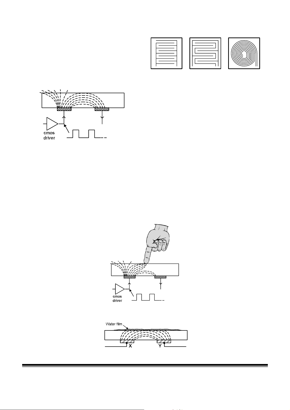
The QT60161B digital charge-transfer (“QT”) QMatrix™ IC is designed to detect human touch on up 16 keys when used in
conjunction with a scanned, passive X-Y matrix. It will project the keys through almost any dielectric, e.g. glass, plastic, stone,
ceramic, and even wood, up to thicknesses of 5 cm or more. The touch areas are defined as simple 2-part interdigitated
electrodes of conductive material, like copper or screened silver or carbon deposited on the rear of a control panel. Key sizes,
shapes and placement are almost entirely arbitrary; sizes and shapes of keys can be mixed within a single panel of keys and can
vary by a factor of 20:1 in surface area. The sensitivity of each key can be set individually via simple functions over the SPI or
UART port, for example via Quantum’s QmBtn program, or from a host microcontroller. Key setups are stored in an onboard
eeprom and do not need to be reloaded with each powerup.
The device is designed specifically for appliances, electronic kiosks, security panels, portable instruments, machine tools, or
similar products that are subject to environmental influences or even vandalism. It can permit the construction of 100% sealed,
watertight control panels that are immune to humidity, temperature, dirt accumulation, or the physical deterioration of the panel
surface from abrasion, chemicals, or abuse. To this end the device contains Quantum-pioneered adaptive auto self-calibration,
drift compensation, and digital filtering algorithms that make the sensing function robust and survivable.
The part can scan matrix touch keys over LCD panels or other displays when used with clear ITO electrodes arranged in a matrix.
It does not require 'chip on glass' or other exotic fabrication techniques, thus allowing the OEM to source the matrix from multiple
vendors. Materials such as such common PCB materials or flex circuits can be used.
External circuitry consists of a resonator and a few capacitors and resistors, all of which can fit into a footprint of less than 6 sq. cm
(1 sq. in). Control and data transfer is via either a SPI or UART port; a parallel scan port provides backwards compatibility with
scanned electromechanical keys.
The QT60161B makes use of an important new variant of charge-transfer sensing, transverse charge-transfer, in a matrix format
that minimizes the number of required scan lines. Unlike some older technologies it does not require one sensing IC per key.
The QT60161B is identical to earlier QT60161 in all respects except that the device exhibits lower signal noise. This
device replaces QT60161 parts directly. After December 2003 the QT60161 will no longer be sold.
Automotive panels
Machine tools
lQ
AVAILABLE OPTIONS
A
TQFP Part NumberT
QT60161B-AS-400C to +1050C
Copyright © 2001 Quantum Research Group Ltd
Pat Pend. R1.03/04.03

Contents
1 Overview
2 Signal Processing
3 Circuit Operation
4 Communications Interfaces
5 Commands & Functions
............................................
.......................................
..................................
..................................
....................................
................................
.................................
.......................................
................................
................................
.................................
.....................................
......................................
3.3.1 RFI From X Lines
3.3.2 Noise Coupling Into X lines
3.4.1 RFI From Y Lines
3.4.2 Noise Coupling Into Y Lines
................................
..................................
....................................
..................................
................................
....................................
................................
.....................................
.......................................
..............................
..............................
.................................
...............................
..............................
.............................
g 0x67 - Get Command
p 0x70 - Put Command
s 0x73 - Specific Key Scope
S 0x53 - All Keys Scope
x 0x78 - Row Keys Scope
y 0x79 - Column Keys Scope
..............................
..............................
..............................
..............................
.............................
©Quantum Research Group Ltd.
........................
.........................
...........................
....................
.........................
.............................
............................
............................
...........................
..........................
...........................
.........................
.................
.....................
......................
..........................
..........................
...........................
............................
..........................
..................
.....................
...........................
...........................
4
41.1 Field Flows
41.2 Circuit Overview
41.3 Communications
5
52.1 Negative Threshold
52.2 Positive Threshold
52.3 Hysteresis
52.4 Drift Compensation
62.5 Negative Recalibration Delay
62.6 Detection Integrator
62.7 Positive Recalibration Delay
62.8 Reference Guardbanding
62.9 Adjacent Key Suppression (‘AKS’)
72.10 Full Recalibration
72.11 Device Status & Reporting
7
73.1 Matrix Scan Sequence
73.2 Signal Path
83.3 'X' Electrode Drives
8
8
83.4 'Y' Gate Drives
8
8
83.5 Burst Length & Sensitivity
83.6 Burst Acquisition Duration
93.7 Intra-Burst Spacing
93.8 Burst Spacing
93.9 Sample Capacitors
93.10 Water Film Suppression
93.11 Reset Input
93.12 Oscillator
93.13 Startup / Calibration Times
93.14 Sleep_Wake / Noise Sync Pin (WS)
103.15 LED / Alert Output
113.16 Oscilloscope Sync
113.17 Power Supply & PCB Layout
113.18 ESD / Noise Considerations
11
114.1 Serial Protocol Overview
124.2 SPI Port Specifications
124.3 SPI Slave-Only Mode
134.4 SPI Master-Slave Mode
144.5 UART Interface
154.6 Sensor Echo and Data Response
154.7 Parallel Scan Port
164.8 Eeprom Corruption
17
175.1 Put / Get Direction Commands
17
17
185.2 Scope Commands
18
18
18
18
0 0x30 - Signal for Single Key
1 0x31 - Delta Signal for Single Key
2 0x32 - Reference Value
5 0x35 - Detection Integrator Counts
6 0x36 - Eeprom Checksum
7 0x37 - General Device Status
<sp> 0x20 - Signal Levels for Group
! 0x21 - Delta Signals for Group
" 0x22 - Reference Levels for Group
% 0x25 - Detect Integrator Counts for Group
e 0x65 - Error Code for Selected Key
E 0x45 - Error Codes for Group
k 0x6B - Reporting of First Touched Key
^A 0x01 - Negative Detect Threshold
^B 0x02 - Positive Detect Threshold
^C 0x03 - Negative Threshold Hysteresis
^D 0x04 - Positive Threshold Hysteresis
^F 0x06 - Burst Length
^G 0x07 - Burst Spacing
^H 0x08 - Negative Drift Compensation Rate5
^I 0x09 - Positive Drift Compensation Rate
^J 0x0A - Negative Detect Integrator Limit
^K 0x0B - Positive Recalibration Delay
^L 0x0C - Negative Recalibration Delay
^M 0x0D - Intra-Burst Pulse Spacing
^N 0x0E - Positive Reference Error Band
^O 0x0F - Negative Reference Error Band
^P 0x10 - Adjacent Key Suppression (‘AKS’)
6 0x36 - Eeprom Checksum
L 0x4C - Lock Reference Levels
b 0x62 - Recalibrate Keys
l 0x6C - Return Last Command Character
r 0x72 - Reset Device
V 0x56 - Return Part Version
W 0x57 - Return Part Signature
Z 0x5A - Enter Sleep
^Q 0x11 - Data Rate Selection
^R 0x12 - Oscilloscope Sync
^W 0x17 - Noise Sync
6 Electrical Specifications
7 Mechanical
8 Index
.............................................
...............................
..........................
.......................
.............................
......................
...........................
..........................
.......................
.........................
......................
.................
......................
.........................
....................
..............................
.......................
.......................
....................
.....................
...............................
..............................
.................
..................
...................
.....................
.....................
.......................
....................
...................
..................
....................
...........................
.........................
.............................
...................
...............................
...........................
.........................
................................
..........................
...........................
...............................
.........................
..............................
.................................
............................
..................
................
...............................
.................................
..................
........................................
....................................
.......................................
185.3 Status Commands
18
18
18
18
18
19
19
19
19
19
19
20
20
215.4 Setup Commands
21
21
21
21
21
22
22
22
22
23
23
23
23
23
24
245.5 Supervisory / System Functions
24
24
24
25
25
25
25
25
25
26
26
275.6 Function Summary Table
305.7 Timing Limitations
305.8 Erratta / Notes
31
316.1 Absolute Maximum Specifications
316.2 Recommended operating conditions
316.3 DC Specifications
316.4 Protocol Timing
326.5 Maximum Drdy Response Delays
33
337.1 Dimensions
337.2 Marking
34
lQ
ii
www.qprox.com QT60161B / R1.03

Table 1.1 Device Pin Lis
t
I/O PPMOSI1
I/O PPMISO2
I/O: I = Input
O = Output
Pwr = Power pin
I/O = Bidirectional line
PP = Push Pull output drive
OD = Open drain output drive
©Quantum Research Group Ltd.
DescriptionTypeNamePin
Master-Out / Slave In SPI line. In Master/Slave SPI mode is used for both communication directions.
In Slave SPI mode is the data input (in only).
Master-In / Slave Out SPI line. Not used in Master/Slave SPI mode.
In Slave mode outputs data to host (out only).
SPI Clock. In Master mode is an output; in Slave mode is an inputI/O PPSCK3
Reset input, active low resetIRST4
+5V supplyPwrVdd5
GroundPwrVss6
Oscillator drive output. Connect to resonator or crystal.plyO PPXTO7
Oscillator drive input. Connect to resonator or crystal, or external clock source.IXTI8
UART receive inputIRX9
UART transmit outputO PPTX10
Wake from Sleep / Sync to noise sourceIWS11
Sample output controlO PPSMP12
X0 Drive matrix scan / Communications option A inputI/O PPX0OPA13
X1 Drive matrix scan / Communications option B inputI/O PPX1OPB14
X2 Drive matrix scanO PPX215
X3 Drive matrix scanO PPX316
+5V supplyPwrVdd17
GroundPwrVss18
XS0 Scan input lineIXS019
XS1 Scan input lineIXS120
XS2 Scan input lineIXS221
XS3 Scan input lineIXS322
YS0 Scan output lineO PPYS023
YS1 Scan output lineO PPYS124
YS2 Scan output lineO PPYS225
YS3 Scan output lineO PPYS326
+5 supply for analog sectionsPwrAVdd27
Analog groundPwrAGnd28
+5 supply for analog sectionsPwrAref29
Cs3 control BI/O PPCS3B30
Cs3 control AI/O PPCS3A31
Cs2 control BI/O PPCS2B32
Cs2 control AI/O PPCS2A33
Cs1 control BI/O PPCS1B34
Cs1 control AI/O PPCS1A35
Cs0 control BI/O PPCS0B36
Cs0 control AI/O PPCS0A37
+5 supplyPwrVdd38
GroundPwrVss39
Active low LED status drive / Activity indicatorO PPLED40
Data ready output for Slave SPI mode; active lowO ODDRDY41
Vref input for conversion referenceIVref42
Oscilloscope sync outputO PPSO43
Slave select for SPI direction control; active lowI/O ODSS44
lQ
iii
www.qprox.com QT60161B / R1.03
©Quantum Research Group Ltd.
1 Overview
QMatrix devices are digital burst mode charge-transfer (QT)
sensors designed specifically for matrix geometry touch
controls; they include all signal processing functions
necessary to provide stable sensing under a wide variety of
changing conditions. Only a few low cost external parts are
required for operation. The entire circuit can be built in under
6 square centimeters of PCB area.
Figure 1-1 Field flow between X and Y elements
overlying panel
X
element
The device has a wide dynamic range that allows for a wide
variety of key sizes and shapes to be mixed together in a
single touch panel. These features permit new types of
keypad features such as touch-sliders, back-illuminated keys,
and complex warped panels.
The devices use an SPI interface running at up to 3MHz rates
to allow key data to be extracted and to permit individual key
parameter setup, or, a UART port which can run at rates to
57.6 Kbaud. The serial interface protocol uses simple
commands; the command structure is designed to minimize
the amount of data traffic while maximizing the amount of
information conveyed.
In addition to normal operating and
setup functions the device can also
report back actual signal strengths
and error codes over the serial
interfaces.
QmBtn software for the PC can be
used to program the IC as well as
read back key status and signal
levels in real time.
A parallel scan port is also provided
that can be used to directly replace
membrane type keypads.
QMatrix technology employs
transverse charge-transfer ('QT')
sensing, a new technology that
senses the changes in an electrical
charge forced across an electrode
set.
Figure 1-3 Fields With a Conductive Film
1.1 Field Flows
Figure 1-1 shows how charge is
transferred across an electrode set
to permeate the overlying panel
material; this charge flow exhibits a
high dQ/dt during the edge
transitions of the X drive pulse. The
Y
elem ent
Figure 1-2 Field Flows When Touched
X
element
Figure 1-4 Sample Electrode Geometries
PARALLEL LINES SERPENTINE SPIRAL
charge driven by the X electrode is partly received onto the
corresponding Y electrode which is then processed. The part
uses 4 'X' edge-driven rows and 4 'Y' sense columns to sense
up to 16 keys.
The charge flows are absorbed by the touch of a human
finger (Figure 1-1) resulting in a decrease in coupling from X
to Y. Thus, received signals decrease or go negative with
respect to the reference level during a touch.
As shown in Figure 1-3, water films cause the coupled fields
to increase slightly, making them easy to distinguish from
touch.
1.2 Circuit Overview
A basic circuit diagram is shown in Figure 1-5. The ‘X’ drives
are sequentially pulsed in groupings of bursts. At the
intersection of each ‘X’ and ‘Y’ line in the matrix itself, where
a key is desired, should be an interdigitated electrode set
similar to those shown in Figure 1-4. See Quantum App Note
AN-KD01, or consult Quantum for application assistance.
The device uses fixed external capacitors to acquire charge
from the matrix during a burst of charge-transfer cycles; the
burst length can be varied to permit digitally variable key
signal gains. The charge is converted to digital using a
single-slope conversion process.
Burst mode operation permits the
use of a passive matrix, reduces RF
emissions, and provides excellent
response times.
Refer to Section 3 for more details
on circuit operation.
1.3 Communications
The device uses two variants of SPI
overlying panel
Y
element
communications, Slave-only and
Master-Slave, a UART interface,
plus a parallel scan interface. Over
the serial interfaces are used a
command and data transfer
structure designed for high levels of
flexibility using minimal numbers of
bytes. For more information see
Sections 4 and 5.
The parallel scan port permits the
replacement of electromechanical
keypads that would be scanned by
a microcontroller; the scan interface
mimics an electromechanical
keyboard’s response.
lQ
4
www.qprox.com QT60161B / R1.03
©Quantum Research Group Ltd.
V
Figure 1-5 Circuit Block Diagram
cc
Opt B
Opt A
QT60161
LED
Scope
Sync
Reset
Wake /
Sync
CS0A
CS0B
SPI
to Host
CS1A
UART
CS1B
to Host
CS2A
CS2B
CS3A
CS3B
Scan Output
VREF
Scan Input
Sample
X0
X1
X2
X3
Sample caps
CS0
CS1
CS2
CS3
Y0 Y1 Y2 Y3
X0
X1
X2
X3
2 Signal Processing
The device calibrates and processes signals using a number
of algorithms specifically designed to provide for high
survivability in the face of adverse environmental challenges.
The QT60161B provides a large number of processing
options which can be user-selected to implement very
flexible, robust keypanel solutions.
2.1 Negative Threshold
See also command ^A, page 21
The negative threshold value is established relative to a key’s
signal reference value. The threshold is used to determine
key touch when crossed by a negative-going signal swing
after having been filtered by the detection integrator (Section
2.6). Larger absolute values of threshold desensitize keys
since the signal must travel farther in order to cross the
threshold level. Conversely, lower thresholds make keys
more sensitive.
As Cx and Cs drift, the reference point drift-compensates for
these changes at a user-settable rate (Section 2.4); the
threshold level is recomputed whenever the
reference point moves, and thus it also is drift
compensated.
The threshold is user-programmed on a per-key
basis using the setup process (Section 5).
The threshold is user-programmed using the setup process
described in Section 5 on a per-key basis.
2.3 Hysteresis
See also command ^C and ^D, page 21
Refer to Figure 1-6. The QT60161B employs programmable
hysteresis levels of 12.5%, 25%, or 50% of the delta between
the reference and threshold levels. There are different
hysteresis settings for positive and negative thresholds which
can be set by the user. The percentage refers to the distance
KEYMATRIX
between the reference level and the threshold at which the
detection will drop out. A percentage of 12.5% is less
hysteresis than 25%, and the 12.5% hysteresis point is closer
to the threshold level than to the reference level.
The hysteresis levels are set for all keys only; it is not
possible to set the hysteresis differently from key to key on
either the positive or negative hysteresis levels.
2.4 Drift Compensation
See also commands ^H, ^I, page 22
Signal levels can drift because of changes in Cx and Cs over
time. It is crucial that such drift be compensated, else false
detections, non- detections, and sensitivity shifts will follow.
The QT60161B can compensate for drift using two setups, ^H
and ^I.
Drift compensation is performed by making the reference
level track the raw signal at a slow rate, but only while there is
no detection in effect. The rate of adjustment must be
performed slowly, otherwise legitimate detections could be
ignored. The devices drift compensate using a slew-rate
limited change to the reference level; the threshold and
hysteresis values are slaved to this reference.
When a finger is sensed, the signal falls since the human
body acts to absorb charge from the cross-coupling between
X and Y lines. An isolated, untouched foreign object (a coin,
or a water film) will cause the signal to rise very slightly due to
the enhanced coupling thus created. These effects are
contrary to the way most capacitive sensors operate.
Once a finger is sensed, the drift compensation mechanism
ceases since the signal is legitimately detecting an object.
Drift compensation only works when the key signal in
question has not crossed the negative threshold level
(Section 2.1).
The drift compensation mechanism can be made asymmetric
if desired; the drift-compensation can be made to occur in
one direction faster than it does in the other simply by setting
^H and ^I to different settings.
Figure 1-6 Detection and Drift Compensation
Reference
2.2 Positive Threshold
See also command ^B, page 21
Hysteresis
Threshold
The positive threshold is used to provide a
mechanism for recalibration of the reference point
when a key's signal moves abruptly to the positive.
These transitions are described more fully in
Section 2.7.
lQ
Output
5
Signal
www.qprox.com QT60161B / R1.03

©Quantum Research Group Ltd.
Drift compensation should usually be set to compensate
faster for increasing signals than for decreasing signals.
Decreasing signals should not be compensated quickly, since
an approaching finger could be compensated for partially or
entirely before even touching the touch pad. However, an
obstruction over the sense pad, for which the sensor has
already made full allowance for, could suddenly be removed
leaving the sensor with an artificially suppressed reference
level and thus become insensitive to touch. In this case, the
sensor should compensate for the object's removal by raising
the reference level quickly.
The drift compensation rate can be set for each key
individually, and can also be disabled completely if desired on
a per-key basis.
Drift compensation and the detection time-outs (Section 2.5)
work together to provide for robust, adaptive sensing. The
time-outs provide abrupt changes in reference location
depending on the duration of the signal 'event'.
2.5 Negative Recalibration Delay
See also command ^L, page 23
If a foreign object contacts a key the key's signal may change
enough in the negative direction, the same as a normal
touch, to create an unintended detection. When this happens
it is usually desirable to cause the key to be recalibrated in
order to restore its function after a time delay of some
seconds.
The Negative Recal Delay timer monitors this detection
duration; if a detection event exceeds the timer's setting, the
key will be recalibrated so that it can function thereafter. The
^L function can be altered on a key by key basis. It can be
disabled if desired by setting the ^L parameter to zero, so that
it will never recalibrate automatically.
2.6 Detection Integrator
See also command ^J, page 22
To suppress false detections caused by spurious events like
electrical noise, the QT60161B incorporates a 'detection
integrator' counter that increments with each detection
sample until a user-defined limit is reached, at which point a
detection is confirmed. If no detection is sensed on any of the
samples prior to the final count, the counter is reset
immediately to zero, forcing the process to restart.
When an active key is released, the counter must count down
to zero before the key state is set to 'off'. Setting a key’s
detection integrator target value to zero disables that key
although the bursts for that key continue normally.
The detection integrator is extremely effective at reducing
false detections at the expense of slower reaction times. In
some applications a slow reaction time is desirable; the
detection integrator can be used to intentionally slow down
touch response in order to require the user to touch longer to
operate the key.
There are 16 possible values for this function.
2.7 Positive Recalibration Delay
See also command ^K, page 23
A recalibration can occur automatically if the signal swings
more positive than the positive threshold level. This condition
can occur if there is positive drift but insufficient positive drift
compensation, or if the reference moved negative due to a
recalibration, and thereafter the signal returned to normal.
As an example of the latter, if a foreign object or a finger
contacts a key for period longer than the Negative Recal
Delay, the key is recalibrated to a new lower reference level.
Then, when the condition causing the negative swing ceases
to exist (e.g. the object is removed) the signal can suddenly
swing back positive to near its normal reference.
It is almost always desirable in these cases to cause the key
to recalibrate to the new signal level so as to restore normal
touch operation. The device accomplishes this by simply
setting Reference = Signal.
The time required to detect this condition before recalibrating
is governed by the Positive Recalibration Delay command. In
order for this feature to operate, the signal must rise through
the positive threshold level (Section 2.2) for the proscribed
interval determined by Setup ^K.
After the Positive Recal Delay interval has expired and the
fast-recalibration has taken place, the affected key will once
again function normally. This interval can be set on a per-key
basis; it can also be disabled by setting ^K to zero.
2.8 Reference Guardbanding
See also commands ^N, ^O, page 23; ‘L’, page 24
The QT60161B provides for a method of self-checking that
allows the host to ascertain whether one or more key
reference levels are 'out of spec'. This feature can be used to
determine if an X or Y line has broken, the matrix panel has
delaminated from the control panel, or there is a circuit fault.
Reference guardbanding alerts the host when the reference
level of a key falls outside of user-defined levels. The
reference guardband is determined as a percent deviation
from the 'locked' reference level for each individual key.
These reference levels can be stored into internal eeprom via
the Lock command 'L' during production; deviations in
reference levels that fall outside the guardbands centered on
these locked reference levels are then reported as key errors.
The amount of guardbanding can be set differently for each
signal direction relative to the stored and locked levels. The
possible settings are from 0.1% to 25.5% of signal reference
in steps of 0.1% as set by commands ^N (positive swings)
and ^O (negative swings). A setting of 0 (zero) disables the
corresponding guardband direction.
Once the L command has recorded all values of signal
reference into eeprom, and if guardbanding is enabled, the
part will compare the actual reference level of each key to its
corresponding guardbands to see if it falls outside of these
limits. If so, either of bits 2 and 3 of command 'e' will be set
for that key. The error will also appear in a bitfield reported
via command 'E'.
lQ
2.9 Adjacent Key Suppression (‘AKS’)
See also command ^P, page 24
The QT60161B incorporates adjacent key suppression
(‘AKS’) that can be enabled on a per-key basis. AKS permits
6
www.qprox.com QT60161B / R1.03
©Quantum Research Group Ltd.
the suppression of multiple key presses based on relative
signal strengths. AKS assists in solving the problem of
surface water which can bridge a key touch to an adjacent
key, causing multiple key presses, causing multiple key
presses even though only one key was touched. This feature
is also useful for panels with tightly spaced keys, where a
fingertip can partially overlap an adjacent key.
AKS works for keys that are AKS-enabled anywhere in the
matrix and is not restricted to physically adjacent keys; the
device has no knowledge of which keys are physically
adjacent. When enabled for a key, adjacent key suppression
causes detections on that key to be suppressed if any other
AKS-enabled key in the panel has a more negative signal
deviation from its reference.
This feature does not account for varying key gains (burst
length) but ignores the actual negative detection threshold
setting for the key. If AKS-enabled keys in a panel have
different sizes, it may be necessary to reduce the gains of
larger keys relative to smaller ones to equalize the effects of
AKS. The signal threshold of the larger keys can be altered to
compensate for this without causing problems with key
suppression.
AKS works to augment the natural moisture suppression
capabilities of the device (Section 3.10), creating a more
robust touch panel.
2.10 Full Recalibration
See also command ‘b’, page 24
The part fully recalibrates one or more keys after the ‘b’
command has been issued to it, depending on the current
scope of the ‘b’ command. The device recalibrates all keys on
powerup, after a hard reset via the RST pin or on power up,
or via a reset using the ‘r’ command. Since the circuit
tolerates a very wide dynamic signal range, it is capable of
adapting to a wide mix of key sizes and shapes having widely
varying Cx coupling capacitances.
If a false calibration occurs due to a key touch or foreign
object on the keys during powerup, the affected key will
recalibrate again when the object is removed depending on
the settings of Positive Threshold and Positive Recal Delay
(Sections 2.2 and 2.7).
Calibration requires 9 full burst cycles to complete, and so the
time it takes is dependent on the burst spacing parameter
(Section 3.8 also, ^G, page 22.
2.11 Device Status & Reporting
See also commands ‘7’, page 19; ‘e’, page 19; ‘E’, page 20;
‘k’, page 20, ‘K’, page 20
The device can report on the general device status or specific
key states including touches and error conditions, depending
on the command used.
Usually it is most efficient to periodically request the general
device status using command ‘7’ first, as the response to this
command is a single byte which reports back on behalf of all
keys. ‘7’ indicates if there are any keys detecting, calibrating,
or in error.
If command ‘7’ reports a condition requiring further
investigation, the host device can then use commands ‘e’, ‘E’,
‘k’ or ‘K’ to provide further details of the event(s) in progress.
This hierarchical approach provides for a concise information
flow using minimal data transfers and low host software
overhead.
3 Circuit Operation
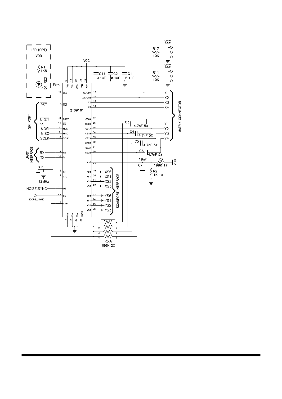
A QT60161B reference circuit is shown in Figure 2-1.
3.1 Matrix Scan Sequence
The circuit operates by scanning each key sequentially, key
by key. Key scanning begins with location X=0 / Y=0. X axis
keys are known as rows while Y axis keys are referred to as
columns. Keys are scanned sequentially by row, for example
the sequence Y0X0 Y0X1 Y0X2 Y0X3 Y1X0 etc.
Each key is sampled from 1 to 64 times in a burst whose
length is determined by Setup ^F. A burst is completed
entirely before the next key is sampled; at the end of each
burst the resulting analog signal is converted to digital using a
single-slope conversion process. The length of the burst
directly impacts on the gain of the key; each key can have a
unique burst length in order to allow tailoring of key sensitivity
on a key by key basis.
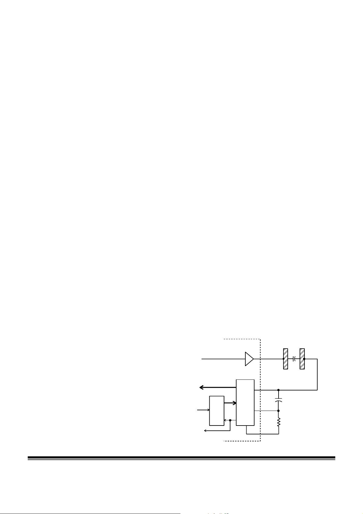
3.2 Signal Path
Refer to Figures 1-5, 3-1, and 3-2.
X-Drives. The X drives are push-pull CMOS lines which drive
charge through the matrix keys on the positive and negative
edges of X. Only the positive edge of X is used for signal
purposes, however the negative edge must cause the charge
across the keys to neutralize prior to the next positive edge,
else the sampling mechanism will cease after one pulse. The
part accomplishes this by holding all Y lines to ground during
the falling edge of X.
Charge gate. Only one X row is pulsed during a burst.
Charge is coupled across a key's Cx capacitance from the X
row to all Y columns. A particular key is chosen by gating the
charge from a single Y column into a single one of four
possible sampler capacitors. The other three X and three Y
lines are clamped to ground during this process.
Dwell time. The dwell time is determined internally and is
the same as one oscillator period, i.e. 83.3ns with a 12MHz
resonator. The dwell time is set via internal switching action
Figure 3-1 QT60161B Circuit Model
X drive
Start
Result
(1 of 4)
X
electrode
CSA
14 bit ADC
CSB
Done
Single-slope
SMP
Burst
Control
Cx
X
Y line (1 of 4)
Cs (1 of 4)
Rs (1 of 4)
Y
electrode
lQ
7
www.qprox.com QT60161B / R1.03

©Quantum Research Group Ltd.
which limits the interval during which charge can be accepted
by a Cs capacitor after the rise of an X drive line.
Dwell time has a dramatic effect on the suppression of
moisture films as described in Section 3.10.
Cs Charge Integrator capacitor. The Cs capacitors
integrate charge arriving through the matrix keys' Cx
capacitances, correspondent with the rise of X; to do this a
switching arrangement on the Cs control pins permits the
charge to accumulate so that the B side of the Cs capacitors
becomes negative when the A side is clamped to ground.
Charge conversion. At the end of each burst the voltage on
Cs is converted to digital by means of a single-slope
conversion process, using one of the external resistors to
ramp up the capacitor towards a reference voltage. The
elapsed time required to reach the comparison voltage is the
digital result. The time required to perform the conversion
depends on Cs, Cx, Rs, Aref, and the burst length.
3.3 'X' Electrode Drives
The 'X' lines are directly connected to the matrix without
buffering. The positive edges of these signals are used to
create the transient field flows used to scan the keys. Only
one X line is actively driving the matrix for scanning purposes
at a time, and it will pulse repetitively for a ‘burst length’ for
each key as determined by the 'Burst Length' Setups
parameter (see command ^F, page 21 and Section 3.5).
3.3.1 RFI F
X drive lines will radiate a small amount of RFI. This can be
attenuated if required by using series resistor in-line with
each X trace; the resistor should be placed near to the
QT60161B. Typical values can range from 100 to 500 ohms.
Excessive amounts of R will cause a counterproductive drop
in signal strength. RC networks can also be used as shown in
Figure 4-6.
Resistance in the X lines also have the positive effect of
limiting ESD discharge currents (Section 3.18).
3.3.2 N
External noise, sometimes caused by ground bounce due to
injected line noise, can couple into the X lines and cause
signal interference in extreme cases. Such noise can be
readily suppressed by the use of series resistors as
described above. Adding a small capacitor to the matrix line
on the QT60161B side of the R, for example 100pF to ground
near the QT60161B, will greatly help to reduce such effects.
ROM
X L
INES
OISE COUPLING INTO
X
LINES
3.4 'Y' Gate Drives
There are 4 'Y' gate drive pairs (CS0A,B..CS3A,B); only one
pair of these lines is used during a burst for a particular key.
The magnitude of the voltages accumulated on the Cs
capacitors should never exceed 0.25V.
3.4.1 RFI F
Y lines are nearly 'virtual grounds' and are negligible radiators
of RFI; in fact, they act as ‘sinks’ for RFI emitted by the X
lines. Resistors are not required in the Y lines for RFI
suppression, and in fact can introduce cross-talk among keys
if large enough. However, small resistance values can be
beneficial to limit ESD transients and make the circuit more
resistant to external RF fields (Section 3.18).
3.4.2 N
External noise, sometimes caused by ground bounce due to
power line noise, can couple into the Y lines and cause signal
ROM
Y L
INES
OISE COUPLING INTO
Y L
INES
interference in extreme cases. Such noise can be readily
suppressed by adding a 22pF capacitor from each Y line to
ground near the QT60161B.
3.5 Burst Length & Sensitivity
See also Command ^F, page 21
The signal gain in volts / pF of Cx for each key is controlled
by circuit parameters as well as the burst length.
The burst length is simply the number of times the
charge-transfer (‘QT’) process is performed on a given key.
Each QT process is simply the pulsing of an X line once, with
a corresponding Y line gated so as to capture the resulting
charge passed through the key’s capacitance Cx.
QT60161B devices use a finite number of QT cycles which
are executed in a short burst. There can be from 1 to 64 QT
cycles in a burst, in accordance with the list of permissible
values shown on page 21. If a key's burst length is set to
zero, that burst is disabled but its time slot in the scanning
sequence of all keys is preserved so as to maintain scan
timing.
Increasing burst length directly affects key sensitivity. This
occurs because the accumulation of charge on Cs is directly
linked to the burst length. The burst length of each key can be
set individually, allowing for direct digital control over the
signal gains of each key, indivudally.
Apparent touch sensitivity is also controlled by the Negative
Threshold setting (Section 2.1). Burst length and negative
threshold interact; normally burst lengths should be kept as
short as possible to limit RF emissions, but the threshold
setting should normally be kept above a setting of 6 to limit
false detections. The detection integrator can also prevent
false detections at the expense of slower reaction times
(Section 2.6).
The value of Rs also affects sensitivity. Higher values of Rs
will lead to larger values of ADC result and higher conversion
gains. The side effect of this is that the conversion will take
longer and timing conflicts can occur (Section 3.6).
Cs does not significantly affect gain. Smaller values of Cs will
have higher delta signal voltages but this gain increase is
offset by the decrease in gain caused by a steeper ADC
conversion slope. However smaller values of Cs lead to faster
conversion times for a given value of Rs, which in turn allows
for more relaxed burst timings. Smaller values of Cs also
reduce the dynamic range of the system, meaning that the
acquisition becomes less tolerant of high values of Cx, due to
earlier saturation of the voltage across Cs.
3.6 Burst Acquisition Duration
The total time required to acquire a key's signal depends on
the burst length for that key plus the time required to convert
the voltage on the corresponding Cs capacitor to digital. The
conversion is performed via a single-slope ADC process
using one of the external Rs resistors.
If the total time required for the acquisition, i.e. the burst
length plus ADC times plus the signal processing and serial
interface command handler times exceed the burst spacing
setup parameter (Section 3.8), significant timing errors and
communications problems can occur.
The time taken by the burst itself is straightforward to
quantify, but the time required to do the ADC step is not. The
ADC step depends on the value of Vref (pin 42), Cs, Rs, and
lQ
8
www.qprox.com QT60161B / R1.03

©Quantum Research Group Ltd.
Cx. Therefore it is vital that the circuit be checked with an
oscilloscope to make sure that burst spacings are unaffected
during normal operation.
3.7 Intra-Burst Spacing
See also Command ^M, page 23
The time between X drive pulses during a burst is the
intra-burst pulse QT spacing. This timing has no noticeable
effect on performance of the circuit, but can have an impact
on the nature of RF spectral emissions from the matrix panel.
The setting of this function can be from 1µs to 10µs, loosely
corresponding to fundamental emission frequencies of from
1MHz to 100kHz respectively.
Longer spacings require more time to execute and can limit
the operational settings of burst length and/or burst spacing
(Section 5.7).
The intra-burst QT spacing has no effect on sensitivity or
water film suppression and is not particularly important to the
sensing function other than described above.
3.8 Burst Spacing
See also Command ^G, page 22
The interval of time from the start of one burst to the start of
the next is known as the burst spacing. This is an alterable
parameter which affects all keys.
Shorter spacings result in faster response time, but due to
increasing timing restrictions at shorter spacings burst
lengths or the conversion resolution may be restricted,
limiting the amount of gain that can be obtained; see Sections
3.6 and 5.7. Conversely longer spacings permit higher burst
lengths but slow down response time.
Three settings of burst spacing are possible: 500µs, 1ms, and
2ms.
3.9 Sample Capacitors
Charge sampler capacitors Cs should be either ceramic NPO,
X7R 5%, or PPS film for stability reasons.
The values of capacitance should not be altered from that
shown in the schematic of Figure 3-2 without good reason.
Changes in Cs have only a limited effect on signal gain.
3.10 Water Film Suppression
Water films on the user surface can cause problems with
false detection under certain conditions. Water films on their
own will not normally cause false detections. The most
common problem occurs when surface water bridges over 2
or more keys, and a user touches one of the keys and the
water film causing an adjacent key to also trigger. Essentially,
the water film transports the touch contact to adjacent keys.
The circuit suppresses water coupling by having a short dwell
time, equal to one oscillator period or 83ns. A short dwell time
reduces the amount of charge collected via resistive water
films, i.e. it suppresses charge from areas adjacent to the
scanned key. This effect has nothing to do with the frequency
of the burst itself.
Very short dwell times can cause excess suppression of
human touch as well. If series resistors are used in line with
the X and Y matrix lines for noise and ESD suppression
(Section 3.18), a short dwell time can seriously affect signal
gain.
Mechanical measures can also be used to suppress key
cross-coupling, for example one can use raised plastic
barriers between keys, or placing keys in shallow wells to
lengthen the electrical path from key to key.
3.11 Reset Input
The RST’ pin can be used to reset the device to simulate a
power down cycle, in order to bring the part up into a known
state should communications with the part be lost. The pin is
active low, and a low pulse lasting at least 10µs must be
applied to this pin to cause a reset.
To provide for proper operation during power transitions the
devices have an internal brown-out detector set to 4 volts.
A reset command, ‘r’, is also provided which generates an
equivalent hardware reset (page 25).
3.12 Oscillator
The oscillator can use either a quartz crystal or a ceramic
resonator. In either case, the XTI and XTO must both be
loaded with 22pF capacitors to ground. 3-terminal resonators
having onboard ceramic capacitors are commonly available
and are recommended. An external TTL-compatible
frequency source can also be connected to XTI; XTO should
be left unconnected.
The frequency of oscillation should be 12MHz +/-2%.
3.13 Startup / Calibration Times
The QT60161B requires initialization times as follows:
1. From very first powerup to ability to communicate:
2,000ms (One time event to initialize all of eeprom)
2. Normal cold start to ability to communicate:
70ms (Normal initialization from any reset)
3. Calibration time per key vs. burst spacings:
spacing = 500µs: 100ms
spacing = 1ms: 150ms
spacing = 2ms: 300ms
To the above, add 2,000ms or 70ms from (1) or (2) for
the total elapsed time from reset to ability to report key
detections.
Keys that cannot calibrate for some reason require 5
calibration cycles before they report as errors. However, the
device can report back during this interval that the key(s)
affected are still in calibration via status function bits.
3.14 Sleep_Wake / Noise Sync Pin (WS)
The Sleep_wake and Noise sync features use input pin WS.
The Sleep and Sync features can be used simultaneously;
the part can be put into Sleep mode, but awakened by a
noise sync signal which is gated in at the time desired.
Sleep mode: See also command ‘Z’, page 25. The device
can be put into an ultra low-power sleep mode using the ‘Z’
command. When this command is received, the WS pin must
be placed immediately thereafter into a logic-high state. The
part will complete an ongoing burst before entering Sleep.
The part can be awakened by a low transition on the WS pin
lasting at least 5µs. One convenient way to wake the part is
to connect WS to MOSI, and have the host send a null
lQ
9
www.qprox.com QT60161B / R1.03
©Quantum Research Group Ltd.
Figure 3-2 Recommended Circuit Diagram
command to the device. The part will wake and the null
command will not be processed. The MOSI line in turn
requires a pullup resistor to prevent the line from floating low
and causing an unintentional wake from sleep.
During Sleep the oscillator is shut down, and the part
hibernates with microamp levels of current drain. When the
part wakes, the part resumes normal functionality from the
point where it left off. It will not recalibrate keys or engage in
other unwarranted behavior.
Just before going to sleep the part will respond with a
response of 'Z'. In slave-only SPI mode (see Section 4.3), the
SS line must be floated high by the host as soon as it
receives this response; if SS does not float high, sleep will fail
and the device will instead completely reset after about 2
seconds. Upon waking the part will issue another 'Z' byte
back to the host.
Noise sync: See also command ^W,
page 26. External fields can cause
interference leading to false
detections or sensitivity shifts. The
strongest external fields usually
come from AC power. RF noise
sources are heavily suppressed by
the low impedance nature of the QT
circuitry itself.
External noise only becomes a
problem if the noise is uncorrelated
with signal sampling; uncorrelated
noise can cause aliasing and beat
effects in the key signals. To
suppress this problem the devices
feature a noise sync input which
allows bursts to synchronize to the
noise source. This same input can
also be used to wake the part from a
low-power Sleep state.
The device’s bursts can be
synchronized to an external source
of repetitive electrical signal, such as
50Hz or 60Hz, or possibly a video
display vertical sync line, using the
Sleep_wake / Noise sync line. The
noise sync operating mode is set by
command ^W. This feature allows
dominant external noise signals to
be heavily suppressed, since the
system and the noise become
synchronized and no longer beat or
alias with respect to each other. The
sync occurs only at the burst for key
0 (X0Y0); the device waits for the
sync signal for up to 100ms after the
end of a preceding full matrix scan
(after key #15), then when a negative
sync edge is received, the matrix is
scanned in its entirety again.
The sync signal drive should be a
buffered logic signal, or perhaps a
diode-clamped signal, but never a
raw AC signal from the mains.
Since Noise sync is highly effective
yet simple and inexpensive to implement, it is strongly
advised to take advantage of it anywhere there is a possibility
of encountering electric fields. Quantum’s QmBtn software
can show signal noise caused by nearby AC electric fields
and will hence assist in determining the need to make use of
this feature.
If the sync feature is enabled but no sync signal exists, the
sensor will continue to operate but with a delay of 100ms
from the end of one scan to the start of the next, and hence
will have a slow response time.
3.15 LED / Alert Output
Pin 40 is designed to drive a low-current LED, 5mA
maximum, in an active-low configuration. Higher currents can
cause significant level shifts on the die and are not advised.
The LED will glow brightly (i.e. pin 40 will be solid low) during
calibration of one or more keys, for example at startup. When
a key is detected, the LED will pulse low for the duration of
lQ
10
www.qprox.com QT60161B / R1.03

©Quantum Research Group Ltd.
the burst during which the key is being sensed, i.e. with a
very low duty cycle. Each additional key being detected will
also create a low pulse for that key’s burst. During all other
times, the LED pin will be off (high).
This pin can be used to alert the host that there is key activity,
in order to further limit the amount of communication between
the device and the host. The LED / Alert line should ideally be
connected to an interrupt pin on the host that can detect a
negative edge, following which the host can proceed to poll
the device for keys.
This line also pulls low if there is a key error of any kind.
Note that in sleep mode if the LED was on prior to sleep, it
will remain on during sleep.
3.16 Oscilloscope Sync
See also Command ^R, page 26
The ‘SO’ pin can output an oscilloscope sync signal which is
a positive pulse that brackets the burst of a selected key. This
feature is controlled by the ^R command. More than one burst
can output a sync pulse, for example if the scope of the
command when set is a row or column, or is all keys. The ^R
command is volatile and does not survive a reset or power
down.
This feature is invaluable for diagnostics; without it, observing
signals clearly on an oscilloscope for a particular burst is
nearly impossible.
This function is supported in QmBtn PC software via a
checkbox.
3.17 Power Supply & PCB Layout
Vdd should be 5.0 volts +/- 5%. This can be provided by a
common 78L05 3-terminal regulator. LDO type regulators are
often fine but can suffer from poor transient load response
which may cause erratic signal behavior.
If the power supply is shared with another electronic system,
care should be taken to assure that the supply is free of
low-level spikes, sags, and surges which can adversely affect
the circuit. The devices can track slow changes in Vcc
depending on the settings of drift compensation, but signals
can be adversely affected by rapid voltage steps and impulse
noise on the supply rail.
Supply bypass capacitors of 0.1uF to a ground plane should
be used near every supply pin of every active component in
the circuit.
PCB layout: The PCB layout should incorporate a ground
plane under the entire circuit; this is easily possible with a
2-layer design. The ground plane should be broken up as
little as possible. Internal nodes of the circuit can be quite
sensitive to external noise and the circuit should be kept
away from stray magnetic and electric fields, for example
those emanating from mains power components such as
transformers and power capacitors. If proximity to such
components is unavoidable, an electrostatic shield may be
required.
The use of the Sync feature (Section 3.14) can be invaluable
in reducing these types of noise sources, but only up to a
point.
3.18 ESD / Noise Considerations
In general the QT60161B will be well protected from static
discharge during use by the overlying panel. However, even
with a dielectric panel transients currents can still flow into
scan lines via induction or in extreme cases, dielectric
breakdown. Porous or cracked materials may allow a spark to
tunnel through the panel. In all cases, testing is required to
reveal any potential problems. The IC has diode protected
pins which can absorb and protect the device from most
induced discharges, up to 5mA.
The X lines are not usually at risk during operation, since they
are low-resistance output drives. Diode clamps can be used
on the X and Y matrix lines if desired. The diodes should be
high speed / high current types such as BAV99 dual diodes,
connected from Vdd to Vss with the diode junction connected
to the matrix pin. Diode arrays can also be used.
Capacitors placed on the X and Y matrix lines can also help
to a limited degree by absorbing ESD transients and lowering
induced voltages. Values up to 100pF on the X lines and
22pF on the Y lines can be used.
The circuit can be further protected by inserting series
resistors into the X and/or Y lines to limit peak transient
current. RC networks as shown in Figures 4-6 and 4-7 can
provide enhanced protection against ESD while also limiting
the effects of external EMI should this be a problem.
External field interference can occur in some cases; these
problems are highly dependent on the interfering frequency
and the manner of coupling into the circuit. PCB layout
(Section 3.17) and external wiring should be carefully
designed to reduce the probability of these effects occurring.
SPI / UART data noise: In some applications it is necessary
to have the host MCU at a distance from the sensor, perhaps
with the interface coupled via ribbon cable. The SPI link is
particularly vulnerable to noise injection on these lines;
corrupted or false commands can be induced from transients
on the power supply or ground wiring. Bypass capacitors and
series resistors can be used to prevent these effects as
shown in Figures 4-6 and 4-7.
4 Communications Interfaces
The QT60161B uses parallel, UART, and SPI interfaces to
communicate with a host MCU. The serial interfaces use a
protocol described in Section 5. Only one interface can be
used at a time; the interface type is selected by
resistor-coupled jumpers connected to pins X0OPA (pin 13)
and X0OPB (pin 14) shown in Table 4-1. See also Figure 3-2.
Further specific information on each interface type is
contained in the following sections:
SPI Slave-Only Mode: Section 4.3
SPI Master-Slave Mode: Section 4.4
UART Interface: Section 4.5
Parallel Interface: Section 4.7
4.1 Serial Protocol Overview
The SPI and UART interface protocols are based entirely on
polled data transmission, that is, the part will not send data to
the host of its own volition but will do so only in response to
specific commands from a host.
lQ
11
www.qprox.com QT60161B / R1.03

©Quantum Research Group Ltd.
Run-time data responses, such as key detection or error
information, requires simple single-byte functions to evoke a
response from the part.
Setup mode interactions mostly use 2-byte functions from the
host to cause the part to alter its behavior; these functions
also cause writes to the internal eeprom.
The concept of 'scope' is used to allow functions to operate
on individual keys or groupings of keys. The scope of
subsequent functions can be altered by short initial scope
instructions.
See Section 5 for protocol details.
4.2 SPI Port Specifications
The part has an SPI synchronous serial interface with the
following specifications at 12MHz oscillator frequency:
Max clock rate, Fck 3MHz
Data length 8 bits
Host command space, Tcm m 50µs
Response delay to host, Tdr1 Table 4-1, also, Sec. 6
Drdy delay from response, Tdr2 1µs to 1ms
Multi-byte return spacing, Tdr3 10µs to 2ms
The host can clock the SPI with the part in Slave mode at any
rate up to and including the maximum clock rate Fck. The
maximum clock rate of the part in Master mode is determined
by Setup ^Q (page 25).
The part can operate in either master-slave mode or
slave-only mode, and is thus compatible with virtually all
SPI-capable microcontrollers.
The SPI interface should not be used over long distances due
to problems with signal ringing and introduced noise etc.
unless suitably buffered or filtered with RC networks as
shown in Figures 4-6 and 4-7. Slower data rates with longer
RC timeconstants will provide enhanced resistance to noise
and ringing problems.
4.3 SPI Slave-Only Mode
Refer to Figures 4-1, 4-3 and 4-2. In Slave-only mode the
host must always be in Master mode, as it controls all SPI
activity including the clocking of the interface in both
directions. Unlike hardware SPI slaves, the QT60161B needs
processing time to respond to functions. DRDY’ is used to let
the host know when data is ready for collection; it indicates to
the host when data is ready in response to a command so
that the host can clock over the data.
This mode requires 5 signals to operate:
MOSI - Master out / Slave in data pin; used as an input for
data from
connected to the MOSI pin of the host device.
MISO - Master in / Slave out data pin; used as an output for
data to
to the MISO pin of the host device.
SCK - SPI clock - input only clock pin from host. The host
must shift out data on the falling edge of SCK; the
QT60161B clocks data in on the rising edge of SCK.
Important note: SCK must idle low just before and after
SS’ transitions either up or down, or the transmission will
fail; between bytes SCK should idle low.
SS’ - Slave select - input only; this pin acts as a framing
signal to the sensor from the host. This line must go low
the host at all times. This pin should be
the host at all times. This pin should be connected
just before and during reception of data from the host. It
must not go high again until the SCK line has returned low;
during data or echo response it must not go high until after
the host has sensed that DRDY’ has gone high from the
device. This pin must idle high. The SS’ pin has an internal
pullup resistor inside.
DRDY’ - Data Ready - active-low - indicates to the host that
the part is ready to send data back subsequent to a
command from the host. This pin idles high. The DRDY’
pin has an internal pullup resistor inside.
Internal pullup resistors note: The internal pullup resistors
can range from 35k to 120k ohms. If RC filtering is used on
the SPI lines per Figure 4-6, this resistance may not be low
enough to ensure adequate signal risetime and may need to
be augmented with external 10k pullups.
The host must wait until DRDY’ goes low before an SPI
transfer to retrieve data. For multi-byte responses, the host
must observe DRDY' to see when it goes high again after
each data byte, then low again, before executing another
transfer to get the next data byte. The host should send null
bytes (0x00) to retrieve data.
If the DRDY’ line does not go low after a command, the
command was not properly received or it was inappropriate.
The delay to DRDY’ low depends on the command and how
many bytes of data are being stored into eeprom; Table 4-1
shows the maximum delays encountered in most cases.
Absolute worst case delays are found in Section 6-5; these
timings occur only rarely, for example if the device happens
to be busy with adjacent key suppression calculations, which
occurs only at the moment when a key is first detected.
A typical Slave-only function sequence is as follows:
1) The host pulls SS’ low, then transfers a command to the
sensor. The host then releases SS’ to float high. DRDY’ is
unaffected in this step.
2) For 2-byte functions, (1) is repeated with a m50us delay.
3) When the sensor has the command echo or requested
data ready to send back to the host, it loads it into its SPI
register and pulls DRDY’ low.
4) The host detects that the sensor has pulled DRDY’ low
and in turn the host pulls SS’ low.
5) The host obtains the byte from the sensor by transmitting
a dummy byte (0x00) to the sensor.
6) The sensor releases DRDY’ to float high.
7) After the host detects that DRDY' has floated high the
host must allow SS’ to also float high.
8) For multi-byte responses, steps (3) through (7) are
repeated until the return data is completely sent.
Note that the host must release the SS’ line in step (7) even
between multiple byte responses because the QT60161B
waits for the SS’ line to return high before signalling that the
next byte is ready for collection.
Note also that the host should check the DRDY’ line and wait
for it to go high before transmitting another byte. Until the
DRDY’ line is released the sensor is still processing a data
return, even if the complete response data has been fully
transferred; the sensor may still be busy when the host
finishes the byte transfer and may not be able to digest a new
command immediately.
lQ
12
www.qprox.com QT60161B / R1.03

©Quantum Research Group Ltd.
Q
x
x
x
x
V
See Section 3.15, page 10, for a description of the Alert pin
which can be used to reduce communication traffic.
4.4 SPI Master-Slave Mode
Refer to Figures 4-1, 4-2, and 4-4. In Master-Slave mode the
host and the sensor take turns being Master, with the host
always leading off in Master mode during an exchange. The
current Master always controls all 3 signal lines. The sensor
takes a variable amount of time to respond to the host,
depending on the nature of the function and its current and
pending tasks. The host, like the sensor, must idle in slave
mode when not sending a command.
Master/Slave requires 3 signals to operate:
MOSI - Master out / Slave in data pin - bidirectional - an input
pin while the host is transmitting data; an output when the
sensor is transmitting data. The MOSI of the host and
slave should be tied together. The MISO lines are not used
on either part and should be left open.
SCK - SPI clock - bidirectional - an input pin when receiving
data; an output pin when sending. The host must shift out
data on the falling edge of SCK; the QT60161B clocks data
in on the rising edge of SCK. Important note: SCK from
the host must be low before asserting SS’ low or high at
either end of a byte or the transmission will fail. SCK
should idle low; if in doubt, a 10K pulldown resistor should
be used. When the sensor returns data it becomes the
Master; data is shifted out by it on the falling edge of SCK
and should be clocked in by the host on the rising edge.
SS’ - Slave select - bidirectional framing control. When the
sensor is in slave mode, this pin accepts the SS’ control
signal from the host. In either data direction, SS' must go
low before and any during data transfer; it should not go
high again until SCK has returned low at the end of a byte.
In Master mode the sensor asserts control over this line, to
make the host a slave and to frame the data. This line
must idle high; the part includes an internal pullup resistor
and should be floated during idle times.
Internal pullup resistor note: The internal pullup resistor on
SS’ can range from 35k to 120k ohms. If RC filtering is used
on the SPI lines per Figure 4-7, this pullup resistance may not
be low enough to ensure adequate signal risetime and may
need to be augmented with external 10k pullups.
A command may consist of one or two bytes with a m50us
delay between command bytes. At the end of a full command,
the Master must go into Slave mode to await a response from
the sensor.
The sensor may take some time to process the host
command and respond. When it does so, it asserts SS’ low
and begins clocking its data. For multi-byte responses, the
bytes will be sent at intervals which may be somewhat
irregular depending on the request and the processing
load of the sensor. The host must be prepared to accept
the sensor data as it comes or there can be a data
overrun in the host. If the data returns too fast for the host
to accept it, the SPI clock rate should be lowered.
A typical Master-Slave function sequence is as follows:
1) Host enters Master mode. The sensor is already in
Slave mode.
Figure 4-1 Communications Option Jumpers
cc
Opt B
10K10K
To M a t ri x
X0
X1
Opt A
L H H L
13
14
Interface TypeX0OPB (Pin 14)X0OPA (Pin 13)
SPI, Slave onlyLowLow
UARTHighLow
SPI, Master/SlaveLowHigh
ParallelHighHigh
2) The host pulls SS’ low, then transfers one byte of
command to the sensor via MOSI, then releases SS’ to
float high again.
3) For 2-byte functions, (2) is repeated with m50us spacings
between bytes.
4) The host immediately places its SPI port into Slave mode,
floating SCK and MOSI’; SS’ stays floating.
5) When the sensor has a command echo or data to send
back, it puts its SPI register in Master mode, taking control
over MOSI and SCK. SS' remains floating.
6) The sensor pulls SS’ low, then clocks out its response
byte to the host, then floats SS’ high again.
7) The sensor repeats (6) as necessary for multiple byte
responses.
8) The sensor returns to slave mode.
After the transmission sequence, the SPI lines float high or
are left to float in an indeterminate state (MOSI) until the next
transmission sequence is initiated by the host. The host
should wait for >1ms after a sequence before initiating
another transmission sequence.
See Section 3.15, page 10, for a description of the Alert pin
which can be used to reduce communication traffic.
Figure 4-2 SPI Connections
Slave-Only Master-Slave
Host MCU
P_IN
P_OUT
SCK SCK
MOSI MOSI
SS
Vdd
T60
DRDY
SS
MISOMISO
5
Host MCU QT60
SS
SCK SCK
MOSI MOSI
DRDY
SS
MISOMISO
5
lQ
13
www.qprox.com QT60161B / R1.03

©Quantum Research Group Ltd.
T
DRDY
{from sensor}
SS
{from host}
SCK
{from host}
MOSI
{from host}
MISO
{from sensor}
SS
SCK
MOSI
Figure 4-3 SPI Slave-Only Mode Timing
dr3
T
cm
7 6543210
7 6543210 7 6543210
Invalid Data
7 6543210
T
dr1
Optional Byte 2Host Command Byte 1 Null Dummy Data Null Dummy Data
7 6543210 7 6543210
Invalid Data Response Data or Echo Nth Response Data
T
dr2
Figure 4-4 SPI Master/Slave Mode Timing
T
cm
7 6543210 7 6543210 7 6543210 7 6543210
Command Byte 1
from Host to sensor
Optional Byte 2
from host to sensor
T
dr1
Response Byte or Echo
from sensor to host
{N = command dependent}
T
dr3
Nth Byte from sensor
{N = command dependent}
SS, SCK, MOSI originate from Host SS, SCK, MOSI originate from sensor
Floating
Figure 4-5 UART Timing
T
dr1
RX
{from host}
TX
{from sensor}
T
cm
Command Byte 1
from host to sensor
76543210S
Optional Byte 2
from host to sensor
4.5 UART Interface
Refer to Figures 4-1 and 4-5.
UART communications requires only 2 wires, TX and RX to
communicate with a host device. All communications must be
Table 4-1 Typical Tdr1 Response Delays (100µs sample ramp)
Setup - Put (affect 1 key)
Setup - Put (affect 8 keys)
Setup - Put (affect 16 keys)
Lock reference Level (L)
Calibrate command (all keys)
Get key errors (E)
Get keys pushed (K)
All other commands
T
dr3
76543210S
76543210S
Response Byte or Echo
from sensor to host
Nth Byte from sensor
{N = command dependent}
76543210S
initiated by the host. The baud rate is determined by Setup
^Q (page 25); the maximum baud rate with a 12MHz oscillator
is 57.6K. UART communications uses the following settings:
Burst Spacing
2ms1ms500µsFunction Type
10ms10ms10ms
20ms20ms20ms
65ms65ms65ms
65ms65ms65ms
500µs500µs500µs
450µs450µs450µs
350µs350µs350µs
350µs350µs350µs
lQ
14
www.qprox.com QT60161B / R1.03

©Quantum Research Group Ltd.
5
5
Baud rate 9,600 - 57,600
Data length 8 bits
Parity None
Stop bits 1
Host command space, Tcm m 50µs
Response delay to host, Tdr1 Table 4-1,
also, Sec. 6
Multi-byte return spacing, Tdr3 10µs to 2ms
The actual baud rate is determined by Setup ^Q (page 25).
A UART command may consist of one or two bytes with a
m50us delay between command bytes. At the end of a full
command, the host must await a response from the sensor.
The sensor may take some time to process the host
command and respond. When it does so, it sends back its
data. For multi-byte responses, the bytes will be sent at
intervals which may be somewhat irregular depending on the
request and the processing load of the sensor. The host must
be prepared to accept the sensor data as it comes or there
can be a data overrun in the host. If the data returns
too quickly for the host to accept it, the baud rate
should be lowered.
A typical UART communication sequence is as follows:
1) Host sends a byte to the sensor.
2) For 2-byte functions, a m50us delay is inserted by
the host and then the second byte is sent.
3) If the sensor has a command echo or data to send
back, it does so. The delay from step 2 to step 3 is
shown in Table 4-1. The delay between successive
response bytes (if they occur) is parameter Tdr3
noted above.
4) The sensor repeats (3) as necessary for multiple
byte responses.
5) The sensor waits for the next command.
The host should wait for >1ms after a sequence before
initiating another transmission sequence to be sure
that the sensor has completed any residual activities
from the prior command. Commands that are sent to
the host prematurely will be ignored.
4.6 Sensor Echo and Data Response
Xn
The devices respond to each and every valid
command from the host with at least one return byte.
In the case of functions that do not send data back to
the host, the part returns the command itself as an
echo, but only after the function has been processed to
completion; this also holds for 2-byte functions where
the second byte is an operand: in these cases the
Yn
return byte is an echo of the command, not the
operand.
One important exception to this is the recalibration
command ‘b’ which returns an acknowledgment
immediately rather than prior to the actual
recalibration.
Commands that return data do not send back a
command echo. If desired, the command byte can be
verified via the 'l' (lowercase L) function; see page 25.
The host should not transmit a new command until the
last command has been processed and responded to
completion, plus 1ms.
Commands that are not recognized are ignored, and the host
should monitor for timeouts to detect these conditions. If this
occurs a new command should not be sent until the specified
timeout condition has expired.
The maximum timings shown in Table 4-1 and Section 6-5
are guaranteed provided that the part is operating within its
burst timing limitations described in Section 5.7. If the burst
timing is in violation, the response time to a command may
take considerably longer.
4.7 Parallel Scan Port
The parallel port can be used to directly replace an electromechanical or membrane keyboard. The port is electrically
equivalent to a 4x4 switch matrix with the exception that the
response to a host scan requires up to 100µs. The XS inputs
(pins 19..22) are active high; only one XS line should ever be
driven high at a time (except for error scan, noted below); the
Figure 4-6 Filtering; SPI Slave-Only Connections
+
+
10K
SS
Ca
Ca
Ca
1nF
10K
Ra
Ra
Ra
Ra
Ra
1K
Ca
Ca
(MS not
shown)
Xn
Yn
100
22pF
47pF
220
QT60161 Circuit
X drives
(1 of 4
shown)
Y Lines
(1 of 4
shown)
DRDY
SCK
MISO
MOSI
RESET
Figure 4-7 Filtering; SPI Master-Slave Connections
+5
SS
Ca
Ca
Ca
1nF
10K
Ra
Ra
Ra
1K
Ca
Ca
Ca
(MS not
shown)
QT60161 Circuit
100
22pF
220
47pF
X drives
(1 of 4
shown)
Y Lines
(1 of 4
shown)
DRDY
SCK
MISO
MOSI
RESET
Recommended Values of Ra & Ca for Figures 4-6 and 4-7
Host MCU
P_IN
P_OUT1
SCK
MISO
MOSI
P_OUT2
Host MCU
SS
SCK
MISO
MOSI
P_OUT
CaRaSPI Clock Rate
47pF6803MHz
120pF1,000750kHz
270pF1,000187.5kHz
470pF2,20093.75kHz
lQ
15
www.qprox.com QT60161B / R1.03

©Quantum Research Group Ltd.
output response is found on the YS lines (pins 23..26), and
these are also active high. The bit pattern found on the YS
lines indicates any keys that are touched; like a real matrix,
the device can set multiple bits on the YS lines.
The host should scan to individual lines XS0..XS3. XS0 maps
to matrix drive line X0 (pin 13). The response on YS0 maps to
matrix line Y0. Thus, the scan port logic exactly mimics the
wiring and scanning of the matrix keys.
The parallel scan port operates on a continuous basis, but is
slower to react when either serial port is in operation. If either
serial port is operational, the scan port updates with every
acquisition burst, i.e. 16 times during a complete scan of the
matrix.
For a full-time higher speed scan port response, it should be
enabled as the sole interface via the option jumper settings
shown in Figure 4-1. The port itself is found on pins 19
through 26 (Figure 3-2). In this dedicated mode, the scan port
outputs within 100µs of receiving a scan input from the host.
Error scan: The host can extract error information from the
scan port by setting all XS lines to logical '1' simultaneously.
The part then returns a high level on any YS lines
corresponding to Y matrix lines having key errors. Thus a
single YS bit, if high, could indicate errors on any or all of 4
keys. Errors are reported for the following conditions:
a. Key(s) are currently recalibrating
b. Key(s) tried to calibrate 5 times and failed each time
c. Key(s) signal references are under- or over- limit
It is not possible to determine the cause of the error or
specific key(s) in error via the parallel scan port.
eeprom. As intentional writes in Put mode should only occur
during manufacture, it is normally safe to assume that
eeprom changes during normal run mode are errors.
The host can also periodically test the checksum of the
eeprom as a backup mechanism to the bit 4 error flag.
The uppercase ‘L’ command, Lock Reference Levels, also
writes data to eeprom, and this data also has the potential to
become corrupted. This data is also backed up in Flash so
that it can be recovered, and an error in this data will also set
bit 4 and also alter the checksum. Also, the ‘L’ command only
operates if the device is in Put mode as a further protection.
Flash memory has a limit of 1,000 write cycles, so
copy-to-Flash should not be used often.
4.8 Eeprom Corruption
The device stores its Setup data in an internal eeprom which
can be readily altered via Put mode commands. Sometimes
noise on Vdd, the SPI lines or Reset pin can cause eeprom
corruption which can be difficult or inconvenient to correct.
The device should always be left in Get mode to prevent
spurious commands from corrupting the eeprom. The Get
command should ideally be repeated every second or so to
ensure that if noise on the SPI lines causes a false Put mode
command that it does not last long. Preferably, the ‘l’
command (lowercase ‘L’) should be used to verify that the Put
command has succeeded.
Flash backup: The part backs up the entire eeprom array
into onboard Flash rom after one or more Setup write
commands have been issued and the part is then reset.
During normal operation the part constantly compares the
Flash area with the eeprom array to ensure the two sections
match. If an eeprom error is detected, the device sets an
error flag (bit 4) in the general device status byte (Command
‘7’, page 19) which can be read by the host device. The LED
output also becomes active. If the bit 4 error flag is set, the
host should immediately induce a device reset.
Bit 4 is also set if an intentional write has been made to
eeprom, but not yet copied into Flash via the reset process. It
is perfectly acceptable to continue altering any number of
Setup parameters prior to doing the reset, ignoring this bit.
During power up or after a reset, the device compares the
Flash area with eeprom, and if there is a discrepancy the
eeprom is refreshed from Flash, unless an intentional write
was detected in which case the Flash is updated from the
lQ
16
www.qprox.com QT60161B / R1.03

s
ge
d
e
©Quantum Research Group Ltd.
5 Commands & Functions
The command structure is designed to minimize control and
data traffic. All repetitive data and status commands from the
host are single-byte, and most commands result in singlebyte device responses. Behavioral setup commands involve
multiple bytes but these are infrequently used.
Special 'scope' commands exist to restrict subsequent
commands to a specific key or range of keys. This control
structure permits most matrix keys, which are usually
identical in shape and size, to be programmed 'in bulk' using
a 'global' scope command, followed by a scope restriction to
specific key(s), followed by more key programming, to
prevent the need for tedious key-by-key programming across
an entire matrix.
There are four types of commands:
Direction - Determine whether subsequent commands are
used to get data from or put data to the part;
Scope - Restrict the range of effect of subsequent
commands to a specific set of keys;
Status - Cause the part to respond with key information,
such as detections, signals, error codes, and the like;
Setup - Modify functionality such as burst length, threshold
levels, drift compensation characteristics, etc.
Supervisory - Special functions such as diagnostics,
calibration, etc. which affect the part as a whole.
All command types can be intermixed. Even during normal
device operation it is possible to use Setup and Supervisory
functions to alter key behavior on the fly. There is no special
'setup mode'.
Get/Put, Scope, and many Supervisory functions are volatile
and do not persist after a power down or reset cycle. Some
Supervisory commands require that the part be reset in order
for the new settings to take effect.
Note that the Setup functions write to eeprom and require
extra time for a response back to the host. Also note that as
with all eeprom memories there is a recommended lifetime
limit to the number of writes; this limit is 100,000 cycles.
Command functions are summarized in Section 5-6.
It is highly advised to test the device checksum
(command ‘6’, page 18) or individual settings or the
general device status (‘7’) once Setups have been
programmed into the part, each time the part is powered
up and periodically while running.
The part backs up all eeprom locations into Flash, from
which data is restored automatically following a reset if
eeprom corruption is detected. The part should also be
reset after any Put command(s) in order to force the copy
of eeprom data into Flash. See Section 4.8.
5.1 Put / Get Direction Commands
Setup commands can be used to either send control
information to the part for programming into its internal
eeprom, or to extract the current setting of this information.
The same Setup function can do either. To accomplish this
the device relies on direction control via the Get and Put
commands. In Get mode, a Setup command will return
information. In Put mode, the behavior of the device is
altered, and often a second operand byte must be sent.
The powerup or reset default mode is Get. The current
Get/Put mode persists until countermanded by a different
Get/Put command or until the device is reset or powered off.
It is advisable to use Put mode only when actually writing
Setups to the device, which will happen infrequently; the part
should normally be left in Get mode. Get mode acts as a lock
to prevent accidental changes to the internal eeprom.
Multiple direction commands of the same type (g, g, g, g ...)
are harmless and can be used to insure that the part does not
accidentally enter Put mode for a prolonged period, for
example due to noise glitches on the SPI lines. The 'g'
command can be repeated every few seconds.
g 0X67 - GET C
Scop
Lowercase 'G'. The 'g' command causes the device to treat all
subsequent Setup commands as 'Gets'; after, when a Setup
command is received from the host the part will respond by
sending back the current status of that Setup parameter.
The 'g' command is always single-byte and echoes back
itself.
p 0X70 - PUT C
Lower case 'p'. The 'p' command causes the device to treat
all subsequent Setup commands as 'Puts'; after, when a
2-byte Setup command is received from the host the part will
respond by programming in the desired parameter for the
key(s) which are affected.
The 'p' command is always single-byte and echoes back
itself.
OMMAND
Bytes / Cm
OMMAND
2nd Byte Ran
Return
0x67n/a1n/aPut
n/an/an/an/aGet
Returns2nd Byte RangeBytes / CmdScope
0x70n/a1n/aPut
n/an/an/an/aGet
lQ
17
www.qprox.com QT60161B / R1.03

s
ge
d
e
s
ge
d
e
s
ge
d
e
s
dBy
d
e
s
dBy
d
e
s
dBy
d
e
©Quantum Research Group Ltd.
5.2 Scope Commands
The host should always set the scope parameter when
initializing the part during normal operation as well as during
setup. Scope commands are persistent and apply to all
subsequent functions that are affected by scope, until a
different scope command is issued. On powerup or after reset
the device defaults to scope = 'all keys'.
Many functions only address one key regardless of the
current scope; in these cases the key being addressed is
always the key last set by the ‘s’ or ‘x’ and ‘y’ commands. If
the ‘s’ command was last set to key 9, then even though the
‘S’ command was issued afterwards the one-key scope will
remain key ‘9’. Similarly if ‘x’ was set to 2 and ‘y’ to 3, then
the one-key scope will remain key x=2 / y=3 (key #14). This
rule operates for either Put or Get commands.
Key numbering convention: The numbering of keys goes by
row then column. For example, the key in row X=3, column
Y=1 (X3Y1) is key 7. The formula for conversion of an X-Y
location to a key number is:
key number = X_row + (Y_column x 4)
Row and column numbers are per Fig. 1-5. Keys are acquired
in this same burst sequence, i.e. X0Y0, X1Y0, X2Y0 etc.
s 0X73 - S
Lowercase 'S'. Targets a specific individual key for all further
functions that are affected by scope. The second byte must
contain a binary key number from 0..15.
S 0X53 - ALL K
Uppercase 'S'. Addresses all keys in the matrix for all further
functions that can target a group of keys.
x 0X78 - ROW K
Lowercase 'X'. Targets keys in a specific row for functions
that can address key groups. The second byte must contain a
row number from 0..3.
y 0X79 - C
Lowercase 'Y'. Targets keys in a specific column for functions
that can address key groups. The second byte is a binary
column number from 0..3.
PECIFIC KEY SCOPE
Scop
Scop
Scop
Bytes / Cm
EYS SCOPE
Bytes / Cm
EYS SCOPE
OLUMN KEYS SCOPE
Bytes / Cm
2nd Byte Ran
2nd Byte Ran
2nd Byte Ran
Return
0x730x00..0x0F2n/aPut
n/an/an/an/aGet
Return
0x53n/a1n/aPut
n/an/an/an/aGet
Returns2nd Byte RangeBytes / CmdScope
0x780x00..0x032n/aPut
n/an/an/an/aGet
Return
0x790x00..0x032n/aPut
n/an/an/an/aGet
5.3 Status Commands
Status commands cause the sensor to report back
information related to keys and their signals.
It is not necessary to set the part to Get mode with these
commands, although it is advised to leave the part in Get
mode as a normal precaution (see Section 5.1)
0 0X30 - S
Numeric '0'. Returns the signal level in 16-bit unsigned binary
for one key whose location is determined by scope. The least
significant byte is returned first.
Note that the signal direction is inverted: decreasing values
correspond to more touch due to the physics of key detection
described in Section 1.1.
1 0X31 - D
Numeric '1'. Returns the value {Reference - Signal} in
unsigned 8-bit binary for one key whose location is
determined by scope. If Signal > Reference, the result is
truncated to zero. The return value is also limited to 255
(0xFF).
Increasing amounts of this value correspond to increasing
amounts of touch as the sign of signal is inverted (see 0x30
above).
2 0X32 - R
Numeric '2'. Returns the Reference value in unsigned 16-bit
binary for one key whose location is determined by scope.
The least significant byte is returned first.
5 0X35 - D
Numeric '5'. Returns the Detection Integrator counter value
for one key whose location is determined by scope. This
function is useful primarily for circuit diagnostics.
6 0X36 - E
Numeric '6'. Returns the entire eeprom checksum. This
function is useful primarily for diagnostics and should
periodically be used to check for valid eeprom contents.
The checksum should be computed when the entire device's
settings, including the locked reference levels ('L' command)
are known. The host can then periodically test the checksum
to validate eeprom integrity. If needed, the eeprom can then
IGNAL FOR SINGLE KEY
Scop
ELTA SIGNAL FOR SINGLE KEY
EFERENCE VALUE
ETECTION INTEGRATOR COUNTS
Scop
EPROM CHECKSUM
Scop
tes / Cm
tes / Cm
tes / Cm
# Bytes Rtn
# Bytes Rtn
# Bytes Rtn
Return
n/an/an/a n/aPut
0..0xFFFF211Get
Returns# Bytes RtndBytes / CmdScope
n/an/an/a n/aPut
0x00..0xFF111Get
Returns# Bytes RtndBytes / CmdScope
n/an/an/a n/aPut
0..0xFFFF211Get
Return
n/an/an/a n/aPut
0x00..0xFF111Get
Return
n/an/an/an/aPut
0x00..0xFF11n/aGet
lQ
18
www.qprox.com QT60161B / R1.03

s
dBy
d
e
s
dBy
d
e
s
dBy
d
e
s
dBy
d
e
s
dBy
d
e
©Quantum Research Group Ltd.
be reprogrammed by the host or the device can be reset to
allow the eeprom to be updated from Flash memory (see
Section 4.8).
The checksum is a simple 8-bit carry fold-back type. Changes
to multiple Setups can generate identical checksums.
Changes to one location only will always produce a different
checksum. An identical change to 2, 4, 8, or all 16 keys is
more prone to generating an identical checksum. A unique
checksum can be obtained again by altering any Setup for
another key (i.e. an unused key) to be different.
After any Setups change, the checksum will not be valid until
after the device has been reset.
Note that the status byte returned by the ‘7’ command
contains a bit that is set if there is an error in eeprom data;
this feature operates independently of the checksum
command.
There is no put version of the command.
7 0X37 - G
Section 2.11, p. 7
Numeric '7'. Returns the part's general status byte which is a
4-bit pattern as follows:
Bit 0: 1= one or more keys are in detection
Bit 1: 1= one or more keys are recalibrating
Bit 2: 1= one or more keys are reporting errors
Bit 3: 1= sync fail; the part is not synchronized to an
Bit 4: 1 = Eeprom / Flash contents discrepancy
Higher bits report as 0's and are not used.
This command can be used as a general 1-byte status
response; if one or more bits are set, the host can take
further relevant action to narrow down the specific issue, such
as which key is being touched or in error, via other
commands.
<SP> 0X20 - S
Space character. Same function as 0x30 above except
returns a group response for 4 keys (if Scope = row or
column) or 16 keys (if Scope = 'all keys'). If no group scope
has been selected, returns data for all keys (32 bytes).
Two bytes are returned for each key; the least significant byte
is always returned first.
ENERAL DEVICE STATUS
Scop
external source (if in that mode; see Section 3.14).
Scop
tes / Cm
IGNAL LEVELS FOR GROUP
tes / Cm
# Bytes Rtn
# Bytes Rtn
Return
n/an/an/a n/aPut
0x00..0x1F11n/aGet
Return
n/an/an/a n/aPut
0..0xFFFF8 or 3214, 16Get
" 0X22 - R
Double quote character. Same function as 0x32 above except
returns a group response for 4 or 16 keys depending on
scope. If no group scope has been selected, returns data for
all 16 keys (32 bytes).
% 0X25 - D
Percent character. Same function as 0x35 above except
returns a group response of 4 bytes (Scope = row or column)
or 16 bytes (Scope = 'All keys'). If no group scope has been
selected, returns data for all 16 keys.
e 0X65 - E
Section 2.11, p. 7
Lowercase 'E'. Returns the error byte for a selected key
defined by the 's' command. A 4-bit pattern is returned:
F: 1= failed last full recalibration attempt
R: 1= key is in process of full recalibration
H: 1= key reference is high (above normal bounds)
L: 1= key reference is low (below normal bounds)
u: undefined
Refer also to Section 2.10.
F, Bit 0 is set if it failed to calibrate properly during a forced
recalibration. The sensor will automatically make 5 sequential
attempts at recalibration before setting this flag.
R, Bit 1 is set if the key is in the process of a full
recalibration. When bit 1 is set, bits 2 and 3 are cleared.
H, Bit 2 when set indicates that the key's reference level has
exceeded the upper boundary described in Section 2.8 and
as defined by Command ^N (page 23).
L, Bit 3 when set indicates that the key's reference level falls
below the lower boundary described in Section 2.8 and as
defined by Command ^O (page 23).
If either H or L are set, it means that the key is probably
defective.
EFERENCE LEVELS FOR GROUP
Scop
ETECT INTEGRATOR COUNTS FOR GROUP
Scop
RROR CODE FOR SELECTED KEY
tes / Cm
tes / Cm
# Bytes Rtn
# Bytes Rtn
Return
n/an/an/a n/aPut
0..0xFFFF8 or 3214, 16Get
Return
n/an/an/an/aPut
0x00..0xFF4 or 1614, 16Get
Returns# Bytes RtndBytes / CmdScope
n/an/an/a n/aPut
0x00..0x0F111Get
b0b1b2b3b4b5b6b7
FRHLuuuu
! 0X21 - D
Exclamation character. Same function as 0x31 above except
returns a group response for 4 or 16 keys depending on
scope. If no group scope has been selected, returns data for
all 16 keys (16 bytes). The values returned are limited to the
range 0..255.
lQ
ELTA SIGNALS FOR GROUP
Scop
tes / Cm
# Bytes Rtn
Return
0x00..0xFF4 or 1614, 16Get
n/an/an/a n/aPut
19
www.qprox.com QT60161B / R1.03

s
dBy
d
e
Y
Y
4b5
4b5
s#Bytes
dBy
d
e
s
dBy
d
e
Y0Y
4b5
4b5
©Quantum Research Group Ltd.
E 0X45 - E
RROR CODES FOR GROUP
Scop
tes / Cm
# Bytes Rtn
Return
n/an/an/a n/aPut
0x00..0xFF1 or 411, 4, 16Get
Section 2.11, p. 7
Uppercase 'E'. Returns general error codes for a range of
keys defined by scope. Returns either 1 or 4 bytes depending
on whether a single key, row, column, or entire matrix are
selected.
The bitfields for single key scope are the same as for 'e'
above.
The bitfields for a single row (X) are:
b6b7
3----
b0b1b2b3b
0Y1Y2
The bitfields for a single column (Y) are:
b0b1b2b3b4b5b6b7
X0X1X2X3----
The bitfields for a global response are:
b6b7
X1Y0
X2Y0
X3Y0
----byte1
X3Y1
----byte2
X3Y2
----byte3
X3Y3
----byte4
2
3
7
11
15
X2Y1
6
X2Y2
10
X2Y3
14
X1Y1
X1Y2
X1Y3
b0b1b2b3b
X0Y0
0
1
X0Y1
4
5
X0Y2
8
9
X0Y3
12
13
Byte 1 is the first returned byte in the sequence.
In all the above examples a '1' in a bit position indicates that
there is some type of error associated with the key. The use
of the 'e' command (or 'E' with scope set to a specific key) will
specify the nature of the error.
k 0X6B - R
EPORTING OF FIRST TOUCHED KEY
Scop
tes / Cm
Rtn
Return
n/an/an/a n/aPut
0x00..0xFF11n/aGet
K
0x4B - Key Touch Reporting for Group
Scop
tes / Cm
# Bytes Rtn
Return
n/an/an/a n/aPut
0x00..0xFF1 or 411, 4, 16Get
Section 2.11, p. 7
Uppercase 'K'. Returns 1 or 4 bytes depending on the current
scope. The byte(s) returned contain a bit pattern which
indicates touched keys. A scope of a single key, a row or a
column will return one byte. A scope of all keys will return 4
bytes.
The bitfields for a single key are:
b0b1b2b3b4b5b6b7
key-------
The bitfields for a single row (scope is X) are:
b6b7
b0b1b2b3b
1Y2Y3----
The bitfields for a single column (scope is Y) are:
b0b1b2b3b4b5b6b7
X0X1X2X3----
The bitfields for a global report are:
b6b7
X1Y0
X2Y0
X3Y0
----byte1
X3Y1
----byte2
X3Y2
----byte3
X3Y3
----byte4
2
3
7
11
15
X2Y1
6
X2Y2
10
X2Y3
14
X1Y1
X1Y2
X1Y3
b0b1b2b3b
X0Y0
0
1
X0Y1
4
5
X0Y2
8
9
X0Y3
12
13
Byte 1 is the first returned byte in the sequence.
In all the above examples a '1' in a bit position indicates that
the key is touched; a '0' indicates no touch.
Section 2.11, p. 7
Lowercase 'K'. Returns a byte that indicates which (if any) key
has been touched. The byte is structured as follows:
b0b1b2b3b4b5b6b7
k0k1k2k3---m
Bits are used as follows:
m - if '1', indicates that yet another key is active
k0..k3 - indicates the key number of a first detected key,
in the range 0..15 (0x00..0x0F).
If a reported key drops out while other keys are active, 'k' will
report one of the other active keys, but there is no rule for
which of the next keys gets reported in k0..k5.
If the byte returned has a value of 255 (0xFF), then no key
has been detected.
lQ
20
www.qprox.com QT60161B / R1.03

s
ge
d
e
©Quantum Research Group Ltd.
5.4 Setup Commands
Setup functions are those that alter the behavior a key or a
group of keys. The setups are programmed into eeprom
locations in the part and ordinarily do not need to be
reprogrammed once set. However it is possible to change a
setup while the device is in normal operation without
interrupting the sensing function of the part.24
Setup functions alter the internal eeprom, and this requires a
much longer time to complete than other commands; see
Table 4-1.
Setup 'put' commands become effective immediately after the
echo response of the command byte unless otherwise noted;
some setups require that the key(s) being altered be
recalibrated with the 'b' command (page 24) before they take
effect.
^A 0X01 - N
Section 2.1, p. 5
Ctrl-A. In Put mode, the command followed by a setting is
programmed into eeprom for the key(s) affected by scope.
1, 4, or 16 keys may be affected. Valid decimal values are:
45678101215
17 20 25 30 35 45 55 64
Values other than the above will be rounded down.
In Get mode, the command will return a single byte according
to the current scope rules (Section 5.2).
This controls key sensitivity by setting the counts of signal
delta needed to cause a detect. Higher = less sensitive.
Numbers should be 6 or greater under most conditions to
reduce the probability of noise detection. Numbers greater
than 20 indicate that the burst length is probably too high.
This setup interacts with Burst Length (^F).
^B 0X02 - P
Section 2.2, p. 5
Ctrl-B. In Put mode, the command followed by a setting is
programmed into eeprom for the key(s) affected by scope. 1,
4, or 16 keys may be affected. Valid decimal values are:
45678101215
17 20 25 30 35 45 55 64
Values other than the above will be rounded down.
In Get mode, the command will return a single byte according
to the current scope rules (Section 5.2).
This setup controls the ability of a key to recalibrate quickly
should the signal transition positive quickly, as when a touch
is prolonged enough to cause a recalibration, and when the
key is then 'untouched'. This condition can also be caused by
a foreign object being removed from a key. The value should
normally be set between 6 and 10 counts. If the value is very
EGATIVE DETECT THRESHOLD
ReturnsByte 2 RangeBytes / CmdScope
0x010x04..0x4021, 4, 16Put
0x04..0x40n/a11Get
OSITIVE DETECT THRESHOLD
ReturnsByte 2 RangeBytes / CmdScope
0x020x04..0x4021, 4, 16Put
0x04..0x40n/a11Get
high, the key will still recover by means of the drift
compensation process, albeit more slowly.
^C 0X03 - N
Section 2.3, p. 5
Ctrl-C. In Put mode, the command followed by a setting is
programmed into eeprom for all keys only. The value should
be from 0 to 3, representing hysteresis as follows:
0: 50%
1: 25%
2: 12.5%
3: 0% (no hysteresis)
Values other than the above will be rounded down.
The percentage is the distance from the threshold level to the
reference level. The hysteresis level is always closer to the
threshold point than to the reference point. 25% is a
reasonable value under most conditions.
As this parameter is common to all keys, Put and Get
operations send or return only one byte.
^D 0X04 - P
Section 2.3, p. 5
Ctrl-D. Identical in operation to ^C above except this applies
to positive 'detections' used to recalibrate the sensor (see ^B
above for details). Uses same hysteresis values as ^C above.
^F 0X06 - B
Section 3.5, p. 8
Ctrl-F. In Put mode the command sets the burst length of one
or more keys, according to the current scope. Valid decimal
values are:
012345710
12 15 20 25 30 40 50 64
Values other than the above will be rounded down.
In Get mode, the command will return a single byte according
to the current scope rules (Section 5.2).
^F sets the length of the acquisition burst on a key by key
basis. This setting is directly proportional to signal gain. This
setup interacts with Negative and Positive Threshold (^A and
^B). Increasing ^F can allow for higher threshold levels and
more robust signals, at the expense of increased radiated
emissions and reduced Cx load capacity.
Special condition: If the value for ^F for a key is set to zero
the burst disabled and the key will not function; the key will
report back with an error code. The timing for the 'phantom
burst' will be preserved so that overall key scan timing will
remain unchanged.
EGATIVE THRESHOLD HYSTERESIS
OSITIVE THRESHOLD HYSTERESIS
Scop
URST LENGTH
Bytes / Cm
Byte 2 Ran
ReturnsByte 2 RangeBytes / CmdScope
0x030x01..0x03216Put
0x01..0x03n/a116Get
Return
0x040x01..0x03216Put
0x01..0x03n/a116Get
ReturnsByte 2 RangeBytes / CmdScope
0x060x00..0x4021, 4, 16Put
0x00..0x40n/a11Get
lQ
21
www.qprox.com QT60161B / R1.03

s
ge
d
e
s
ge
d
e
A
s
ge
d
e
©Quantum Research Group Ltd.
^G 0X07 - B
Section 3.8, p. 9
Ctrl-G. In Put mode, sets the spacing between successive
acquire bursts for the entire matrix.
The second byte indicates the spacing to be set according to
the following table:
0: 500µs (0.5ms)
1: 1000µs (1ms)
2: 2000µs (2ms)
Values higher than 2 will be truncated to 2.
Longer delay times equate to slower matrix scanning. At
lower delay times (faster rep rates) there can be conflicts with
long burst lengths and long conversion times which will
prevent proper operation; see also Section 3.6, and Section
5.7.
Burst spacing also affects recalibration time; see Section
2.10.
The scope for this function is always 'all keys'.
^H 0X08 - N
Section 2.4, p. 5
Ctrl-H. In Put mode, sets the rate of drift compensation used
during periods of non-detection, in the negative signal
direction. Valid decimal values are:
1234681012
15 20 25 33 45 60 75 100
Values other than the above will be rounded down.
These numbers correspond to the amount of drift
compensation applied, in 100ms/count of reference change,
for signals which are negative with respect to the reference
level, i.e. in the same direction as legitimate detections.
Higher numbers equate to slower drift compensation.
Overcompensation (too fast) can result in the suppression of
legitimate detections. Under-compensation can result in
inadequate compensation for rapid environmental changes.
Values of 15 to 45 (1.5 to 4.5 secs/count) are considered
normal under most conditions.
Drift compensation does not occur while the signal has
passed below the negative threshold level or subsequently
remained below the negative hysteresis level.
In Get mode, the command will return a single byte according
to the current scope rules (Section 5.2).
The scope in Put mode can be one key, a row or column, or
all keys.
URST SPACING
Scop
Bytes / Cm
EGATIVE DRIFT COMPENSATION RATE
Byte 2 Ran
Return
0x070x00..0x02216Put
0x00..0x02n/a116Get
5
ReturnsByte 2 RangeBytes / CmdScope
0x080x01..0x6421, 4, 16Put
0x01..0x64n/a11Get
^I 0X09 - P
Section 2.4, p. 5
Ctrl-I. Same as ^H above in all respects, except operates
only when the signal is positive with respect to the reference
level, i.e. in an abnormal direction. It is usually desirable to
set this rate much faster than for ^H, i.e. to a lower number.
Valid decimal values are:
1234681012
15 20 25 33 45 60 75 100
Values other than the above will be rounded down.
Values of 4 to 10 (0.4 to 1.0 secs/count) are considered
suitable for most systems.
Positive drift compensation continues to operate even if the
signal has exceeded the positive threshold.
^J 0x0A - N
Section 2.6, p. 6
Ctrl-J. In Put mode, sets the detection integration limit for
one or more keys according to scope.
The unit of measure is a burst, i.e. a setting of 5 means that a
detection must be sensed 5 bursts in sequence. A burst for a
key occurs once every complete matrix scan. The second
byte must be one of the following values (shown in decimal):
0123571015
20 32 45 60 90 123 175 255
Values other than the above will be rounded down.
In Get mode, the command will return a single byte according
to the current scope rules (Section 5.2).
This setup can be used as a noise filter, or as a mechanism
to intentionally slow down key reaction time in order to require
a long user touch.
Special condition: If the value for ^J is set to zero the key is
disabled, but the burst for the key is still generated.
OSITIVE DRIFT COMPENSATION RATE
Scop
Scop
Bytes / Cm
EGATIVE DETECT INTEGRATOR LIMIT
Bytes / Cm
Byte 2 Ran
Byte 2 Ran
0x00..0xFF21, 4, 16Put
Return
0x090x01..0x6421, 4, 16Put
0x01..0x64n/a11Get
Return
0x0
0x00..0xFFn/a11Get
lQ
22
www.qprox.com QT60161B / R1.03

s
ge
d
e
s
ge
d
e
s
ge
d
e
s
ge
d
e
s
ge
d
e
©Quantum Research Group Ltd.
^K 0x0B - P
Section 2.7, p. 6
Ctrl-K. In Put mode, sets the delay until recalibration, timed
from when the signal first crosses the positive threshold.
The second byte controls the delay in 100ms increments, and
must be one of the following valid values:
0123571015
20 32 45 60 90 123 175 255
Values other than the above will be rounded down. As an
example, a value of 60 will cause a 6-second delay.
In Get mode, the command will return a single byte according
to the current scope rules (Section 5.2).
Special condition: If ^K is set to zero this feature is disabled
and the key will never auto-recalibrate on positive transitions;
however drift compensation will still operate.
^L 0x0C - N
Section 2.5, p. 6
Ctrl-L. In Put mode, sets the delay until recalibration, timed
from when the signal first crosses below the negative
threshold as defined by ^A.2.5
The second byte represents the delay in 100ms increments,
and must be one of the following valid values:
0123571015
20 32 45 60 90 123 175 255
Values other than the above will be rounded down. As an
example, a setting of 85 will cause delays of 6 seconds.
In Get mode the function returns a single value only; if scope
is set to row, column, or all, only the value for the lowest
ranking key in the group will be returned.
Special condition: If the value for ^L is set to zero this
feature is disabled and the key will never auto-recalibrate
after a prolonged touch.
^M 0x0D - I
Section 3.7, p. 9
Ctrl-M. In Put mode, sets the amount of time between
individual pulses in a burst.
The second byte must be in the range of 1 to 10 decimal;
other values will be ignored. The setting applies to all keys.
The value corresponds to the timing between pulses within a
burst, in microseconds. For example, a setting of 5 will set the
pulse spacing to 5 microseconds.
In Get mode the function returns the current value of ^M.
OSITIVE RECALIBRATION DELAY
Scop
Scop
Scop
Bytes / Cm
EGATIVE RECALIBRATION DELAY
Bytes / Cm
NTRA-BURST PULSE SPACING
Bytes / Cm
Byte 2 Ran
Byte 2 Ran
Byte 2 Ran
Return
0x0B0x00..0xFF21, 4, 16Put
0x00..0xFFn/a11Get
Return
0x0C0x00..0xFF21, 4, 16Put
0x00..0xFFn/a11Get
Return
0x0D0x01..0x0A216Put
0x01..0x0An/a116Get
Intra-burst pulse spacing controls the fundamental frequency
of the burst and can have a strong effect on radiated
emissions from the matrix control panel. It can also have an
effect on susceptibility to external EMI if the external fields are
close in periodicity to the burst spacing.
^N 0x0E - P
Section 2.8, p. 6
Ctrl-N. In Put mode, sets the amount of tolerable positive
deviation in the reference level for all keys, in tenths of a
percent, with regard to the 'locked' reference value for each
key. The setup is global in nature and affects all keys equally.
Valid values are from 0 to 255 decimal. The percentage
applied is one tenth the operand's decimal value.
In Get mode the function returns the current setting of ^N.
This setup is used to define the limit of possible positive
reference deviation with respect to a factory setting, which is
used in turn to set an error flag for key(s) whose reference
level rises above the designated error band. If for example
this setting is set to 50, and the device is calibrated and
reference levels are locked (see command 'L', Lock
Reference Levels, page 24) into the part by the OEM, then in
the future if the reference level of a key should rise 5% over
its Locked reference level then the key will report back an
error flag via commands 'e' or 'E'.
Guardbands can be used to detect circuit faults as well as
extremes of temperature or moisture on the circuitry.
Special condition: If the value is set to zero, this feature is
disabled.
^O 0x0F - N
Section 2.8, p. 6
Ctrl-O. In Put mode, sets the amount of tolerable negative
deviation in the reference level for all keys, in tenths of a
percent, with regard to the 'locked' reference value for each
key. The setup is global in nature and affects all keys equally.
Valid values are from 0 to 255 decimal. The percentage
applied is equal to the decimal value divided by 10, thus, a
value of 20 equates to a 2% decrease (i.e. the lower
boundary becomes 98% of the locked reference level).
In Get mode the function returns the current setting of ^M.
This setup is identical in nature to ^N except that it governs
negative reference deviations.
Special condition: If the value is set to 0, this feature is
disabled.
OSITIVE REFERENCE ERROR BAND
Scop
Scop
Bytes / Cm
EGATIVE REFERENCE ERROR BAND
Bytes / Cm
Byte 2 Ran
Byte 2 Ran
Return
0x0E0x00..0xFF216Put
0x00..0xFFn/a116Get
Return
0x0F0x00..0xFF216Put
0x00..0xFFn/a116Get
lQ
23
www.qprox.com QT60161B / R1.03

s
ge
d
e
s
e
d
e
©Quantum Research Group Ltd.
^P 0x10 - A
Section 2.9, p. 6
Ctrl-P. In Put mode, instructs logic for the keys specified by
the current scope to suppress a pending touch detection
under certain signal conditions.
Valid 2nd byte values for this function are:
0: AKS off {default}
1: AKS on
In Get mode, the command will return a single byte according
to the current scope rules (Section 5.2).
AKS functions to suppress detections from water films which
can 'spread' a touch signal from the touched key to adjacent
keys.
AKS is also useful for panels with tightly spaced keys, where
a fingertip can partially overlap an adjacent key. This feature
will act to suppress the signals from the unintended key(s).
AKS only operates across keys that have been AKS-enabled;
signal strength comparisons are not made with nonAKS-enabled keys.
Unused keys with burst lengths of zero are also ignored for
purposes of AKS.
DJACENT KEY SUPPRESSION
Scop
Bytes / Cm
(‘AKS’)
Byte 2 Ran
Return
0x100x00, 0x0121, 4, 16Put
0x00, 0x01n/a11Get
5.5 Supervisory / System Functions
Supervisory functions report or control miscellaneous
functions that affect overall chip control, testing, or
diagnostics. All supervisory functions ignore scope except
where noted.
6 0X36 - E
See page 18.
L 0x4C - L
Section 2.8, p. 6
Uppercase 'L'. This is a put-only command that locks the
reference levels of the device into eeprom for all keys, for
boundary checking purposes over the product's life.
The whole command – 'L' followed by a null (0x00) - must be
received within 100ms without any intervening byte, or the
command will fail. The part must be in Put mode for this
command to work.
The scope of this command is always 'all keys'.
This function records to eeprom the signal reference for all
keys. The locked reference levels are used to compute
boundary checks immediately after the command has
finished. The results of this command to not take effect until
the part has been reset.
Due to the large number of bytes written to eeprom by this
command, there is a significant delay from the second byte
until the return echo is sent back to the host.
This command should be used only during production. There
is no get version of the command.
EPROM CHECKSUM
Returns# Bytes RtndBytes / CmdScope
n/an/an/an/aPut
0x00..0xFF11n/aGet
OCK REFERENCE LEVELS
Returns2nd ByteBytes / CmdScope
0x4C0x00216Put
n/an/an/an/aGet
lQ
b 0x62 - R
Section 2.10, p. 7; Section 3.13.
Lowercase 'B'. This is a put-only command that causes the
keys selected by scope to recalibrate. The part must be in Put
mode for this command to work.
The return byte is sent before the keys have calibrated. While
keys are in recalibration, status of the keys can be
determined using the 'e' or 'E' commands.
If 'b' is sent while key(s) are already in the middle of
recalibration, the affected key(s) will abandon the old
calibration cycle and start a new one.
There is no get version of the command.
24
ECALIBRATE KEYS
Scop
Bytes / Cm
2nd Byt
www.qprox.com QT60161B / R1.03
Return
0x62n/a11, 4, 16Put
n/an/an/an/aGet

s
dBy
d
e
s
e
d
e
s
ge
d
e
©Quantum Research Group Ltd.
l 0x6C - R
Lowercase 'L'. This get-only command reports back with the
value of the prior command received by the part. The
command also reports back any erroneous commands,
allowing the host device to verify that a command was
correctly received.
If this command is repeated, the second and subsequent
instances of 'l' will report back with 0x6C.
There is no put version of the command.
r 0x72 - R
Section 3.11, p. 9
Lowercase 'R'. This put-only command hard-resets the part.
The command 0x72 must be followed by a null (0x00) within
100ms or the command will fail. The part must be in Put
mode for this command to work.
A reset occurs about 16ms after the echo byte 0x72 is
transmitted back to the host. The part will resume
communication and sensing in accordance with the timing
shown in Section 3.13.
If for some reason the part is unable to send back the echo
character 0x72, the command will fail.
There is no get version of the command.
V 0x56 - R
Uppercase 'V'. This get-only command returns the part
version number.
There is no put version of the command.
W 0x57 - R
Uppercase 'W'. This get-only command returns the part
signature as follows:
0x10 (16 decimal)
There is no put version of this command.
Z 0x5A - E
Section 3.14, p. 9
Uppercase 'Z'. This put-only command forces the device to
enter sleep mode. The command 0x5A must be followed by a
ETURN LAST COMMAND CHARACTER
Scop
ESET DEVICE
Scop
ETURN PART VERSION
NTER SLEEP
tes / Cm
Bytes / Cm
ETURN PART SIGNATURE
# Bytes Rtn
2nd Byt
Return
n/an/an/an/aPut
0x00..0xFF11n/aGet
Return
0x720x002n/aPut
n/an/an/an/aGet
Returns# Bytes RtndBytes / CmdScope
n/an/an/an/aPut
0x00..0xFF11n/aGet
Returns# Bytes RtndBytes / CmdScope
n/an/an/an/aPut
0x1011n/aGet
Returns2nd ByteBytes / CmdScope
*0x5A, 0x5A0x002n/aPut
n/an/an/an/aGet
null (0x00) within 100ms or the command will fail. The part
must be in Put mode for this command to work.
The command returns 0x5A immediately before going to
sleep, and a second 0x5A upon waking up.
If for some reason the device is unable to transmit the first
return ‘Z’ character back to the host, for example due to the
host not releasing the SS line, the part will completely reset
after about 2 seconds.
The part will reawaken after a logic low is detected for 10µs
on pin 11 (RST’ pin, see Section 3.11). The device then
sends a second ‘Z’ back to the host, and resumes from its
prior state before it went to sleep without the need for
recalibration. The device resumes in Get mode only.
There is no get version of the command.
^Q 0x11 - D
Section 4, p. 11
Ctrl-Q. This is a put-only command that sets the UART baud
rate and the SPI clock rate. All timings assume a 12MHz
oscillator. The part must be in Put mode for this command to
work.
SPI Settings -
The acceptable values of the operand for SPI use are:
0: 93.75 kHz
1: 187.5 kHz
2: 750 kHz
3: 3 MHz
These values define the maximum SPI clock rate in Master
mode (part originates the clock).
Note that when the part is receiving data, the host can send
to the device at rates up to 3MHz even if the rate setting of ^Q
is slower.
Refer to Sections 4.3 and 4.4 for SPI timing details.
New settings do not become effective until the device has
been powered off and back on again or after the reset (‘r’)
command.
UART Settings -
The acceptable values of the operand for UART use are:
0: 9600 baud
1: 14400 baud
2: 19200 baud
3: 38400 baud
4: 57600 baud
There is no get version of this function.
Refer to Section 4.5for UART details.
New settings do not become effective until the device has
been powered off and back on again or after the reset (‘r’)
command.
ATA RATE SELECTION
Scop
Bytes / Cm
2nd Byte Ran
Return
0x110x00..0x042n/aPut
0x00..0x04n/a1n/aGet
lQ
25
www.qprox.com QT60161B / R1.03

s
ge
d
e
©Quantum Research Group Ltd.
^R 0x12 - O
Section 3.16, p. 11
Ctrl-R. In Put mode, controls the oscilloscope sync function
of Pin 43. The settings of this function are:
0: off {factory default}
1: on
When on, Pin 43 outputs a pulse that brackets the acquire
burst(s) for the keys targeted by scope. Without this it is
virtually impossible to view signals on an oscilloscope
corresponding to a specific key.
Pin 43 idles low and pulses high during a sync pulse.
^R is volatile, that is, it does not persist after a power down.
^W 0x17 - N
Section 3.14, p. 9
Ctrl-W. In Put mode, sets whether the noise sync feature is
enabled or disabled. The part must be in Put mode for this
command to work.
The settings are:
0: off {factory default}
1: on
This function has global scope. The default value is 0 (off).
In Get mode this function returns the current setting of ^W.
The setting of ^W does not become effective until the device
has been powered off and back on again or after the reset
(‘r’) command has been issued.
SCILLOSCOPE SYNC
Scop
Bytes / Cm
OISE SYNC
2nd Byte Ran
Return
0x120x00, 0x0121, 4, 16Put
0x00, 0x01n/a11, 4, 16Get
ReturnsByte 2 RangeBytes / CmdScope
0x170x00, 0x012-Put
0x00, 0x01n/a1-Get
lQ
26
www.qprox.com QT60161B / R1.03

lQ
5.6 Function Summary Table
Direction Commands
Get0x67g
Put0x70p
Scope Commands
Status Commands
27
www.qprox.com QT60161B / R1.03
©Quantum Research Group Ltd.
all subsequent Setup commands become 'Gets'
all subsequent Setup commands become 'Puts’
Get ModePut Mode
Operand
P/GDescriptionNameHexChar
Bytes/PutScope Page
Range
0x671-P
0x701-P
0x730x00..0x0F2-Ptargets a specific key in range 0..15Set one key scope0x73s
0x531-Ptargets all keys in the matrixSet all keys scope0x53S
0x780x00..0x032-Ptargets keys in a designated row, range 0..3Set row keys scope0x78x
0x790x00..0x032-Ptargets keys in a designated column, range 0..3Set column keys scope0x79y
ScopeReturns
Bytes
returned
Return
range
0..0xFFFF21Gget signal strength for 1 key signal for 1 key0x300
0..0xFF11Gget Reference-Signal for 1 key delta signal for 1 key0x311
0..0xFFFF21Gget Reference level for 1 key reference for 1 key0x322
0..0xFF11Gget detect integrator for 1 key Det Integrator for 1 key0x350
0..0xFF1-Gget eeprom checksum of entire eepromeeprom checksum0x366
0..0x1F1-Gget device status of entire devicegeneral device status0x377
0..0xFFFF8, 324, 16Gget signal for group signals for group0x20<sp>
0..0xFF4, 164, 16Gget Reference-Signal for group delta signals for group0x21!
0..0xFFFF8, 324, 16Gget References levels for group references for group0x22“
0..0xFF4, 164, 16Gget detection integrators for group Det integrator for group0x25%
0..0x0F11Gget error code for 1 keyerror code for 1 key0x65e
0..0x0F1, 41, 4, 16Gget error bits for group error codes for group0x45E
0..0xFF--Gget indication of first touched keyreport 1st key0x6Bk
0..0x0F1, 41, 4, 16Gget indication of all touched keysreport touches for group0x4BK
Default
setting
Get
Get
undefined
undefined
undefined
undefined
-
-
-
-
-
-
-
-
-
-
-
-
-
-
17
17
18
18
18
18
18
18
18
18
18
19
19
19
19
19
19
20
20
20

g
g
g
y
g
lQ
Setup Commands
Negative threshold0x01^A
Positive threshold0x02^B
Negative hysteresis0x03^C
Positive hysteresis0x04^D
Burst length0x06^F
Burst spacing0x07^G
Neg drift comp rate0x08^H
Pos drift comp rate0x09^I
28
Neg det int limit0x0A^J
www.qprox.com QT60161B / R1.03
Pos recal delay0x0B^K
Neg recal delay0x0C^L
Intra-burst spacing0x0D^M
Pos error band0x0E^N
Neg error band0x0F^O
©Quantum Research Group Ltd.
nal threshold; fewer counts = more sensitive
Si
4, 5, 6, 7, 8, 10, 12, 15, 17, 20, 25, 30, 35, 45, 55, 64
to positive signals for recalibration
sensitivit
4, 5, 6, 7, 8, 10, 12, 15, 17, 20, 25, 30, 35, 45, 55, 64
hysteresis for negative threshold
50%, 25%, 12.5%, 0%
hysteresis for positive threshold
50%, 25%, 12.5%, 0%
sets number of QT cycles / burst; zero disables burst
0, 1, 2, 3, 4, 5, 7, 10, 12, 15, 20, 25, 30, 40, 50, 64
time from start of one burst to start of next burst
rate of drift compensation for ne
0.1, 0.2, 0.3, 0.4, 0.6, 0.8, 1.0, 1.2, 1.5,
rate of drift compensation for positive si
0.1, 0.2, 0.3, 0.4, 0.6, 0.8, 1.0, 1.2, 1.5,
number of detections required to register a touch,
counted in bursts of detection; zero disables a key.
time required to trigger a recal from a positive signal
excursion in 0.1s increments; zero disables recal.
0, 0.1, 0.2, 0.3, 0.5, 0.7, 1.0, 1.5, 2.0, 3.2,
time required to trigger a recal from a detection, in 0.1s
0, 0.1, 0.2, 0.3, 0.5, 0.7, 1.0, 1.5, 2.0, 3.2,
tolerable positive reference deviation with respect to
Locked reference values, step 0.1%. Zero disables.
tolerable ne
Locked reference values, step 0.1%. Zero disables.
500us, 1ms, 2ms
ative signal swings
2.0, 2.5, 3.3, 4.5, 6.0, 7.5, 10 secs
nal swings
2.0, 2.5, 3.3, 4.5, 6.0, 7.5, 10 secs
0, 1, 2, 3, 5, 7, 10, 15, 20, 32,
45, 60, 90, 123, 175, 255 counts
4.5, 6, 9, 12.3, 17.5, 25.5 secs
increments. Zero disables recal.
4.5, 6, 9, 12.3, 17.5, 25.5 secs
period of QT pulses, in microseconds
1, 2, 3, 4, 5, 6, 7, 8, 9, 10us
ative reference deviation with respect to
P/GDescriptionNameHexChar
P/G
P/G
P/G
P/G
P/G
P/G
P/G
P/G
P/G
P/G
P/G
P/G
P/G
P/G
P/Gadjacent key suppression feature; 1 = onKey suppression0x10^P
Get ModePut Mode
Operand
Bytes/PutScope Page
Range
0x00, 0x0121, 4, 16
ScopeReturns
Bytes
returned
110x10
Return
range
Default
setting
0x3C (9s)0x00..0xFF110x0C0x00..0xFF21, 8, 64
210x0C0x04..0x40110x010x04..0x4021, 4, 16
210x080x04..0x40110x020x04..0x4021, 4, 16
210x01 (25%)0x00..0x031160x030x00..0x03216
210x01 (25%)0x00..0x031160x040x00..0x03216
210x0C0x01..0x40110x060x00..0x4021, 4, 16
220 (500us)0x00..0x021160x070x00..0x02216
220x1E (3s)0x01..0x64110x080x01..0x6421, 4, 16
220x0A (1s)0x01..0x64110x090x01..0x6421, 4, 16
220x030x00..0xFF110x0A0x00..0xFF21, 4, 16
230x0A (1s)0x00..0xFF110x0B0x00..0xFF21, 4, 16
23
230x020x02..0x0A1640x0D0x01..0x0A216
230 (off)0x00..0xFF1160x0E0x00..0xFF216
230 (off)0x00..0xFF1160x0F0x00..0xFF216
240 (off)0x00, 0x01

y
y
lQ
Supervisory Commands
Lock references0x4CL
Recal keys0x62b
Reset device0x72r
Sleep0x5AZ
29
www.qprox.com QT60161B / R1.03
Data rate0x11^Q
Scope sync0x12^R
Noise sync0x17^W
©Quantum Research Group Ltd.
locks reference levels into eeprom for future boundar
checks. ‘L’ must be followed by 0x00 (null) 100ms after
the command byte
fully recalibrate keys;
return byte is sent prior to calibration
hard reset the device. ‘r’ must be followed by a null within
100ms.
force device into Sleep mode. ‘Z’ must be followed b
null within 100ms. 0x5A returned before and after
entering Sleep
sets the Master mode SPI clock rate and UART rate;
reset via ‘r’ command or hard reset to take effect
SPI: 93.75kHz, 187.5kHz, 750kHz, 3MHz
UART: 9.6k, 14.4k, 19.2k, 38.4k, 57.6k
oscilloscope sync control. 1 = on.
feature is volatile - does not survive reset
noise sync enable; 1 = on
device must be reset to take effect
a
Get ModePut Mode
Operand
P/GDescriptionNameHexChar
Bytes/PutScope Page
Range
0x002-P
0x4C0x00216P
0x6211, 4, 16P
0x720x002-P
0x5A,
0x5A
ScopeReturns
Bytes
returned
Return
range
0x00..0xFF1-Greturns checksum of internal eepromEeprom checksum0x366
0x00..0xFF1-Gsend back last command byte receivedReturn last command0x6Cl
0x00..0xFF1-Greturns part version numberVersion0x56V
0x101-Greturns part signature numberSignature0x57W
0x00..0x041-0x110x00..0x042-P/G
Default
setting
-
-
-
-
-
-
-
-
0 (93.75k,
9600)
0 (off)0x00, 0x011-0x120x00, 0x0121, 4, 64P/G
0 (off)0x00, 0x011-0x170x00, 0x012-G/P
18
24
24
25
25
25
25
25
25
26
26

©Quantum Research Group Ltd.
r
g
5.7 Timing Limitations
The device requires processing time between bursts, as well
as time to handle communications with the host. With short
burst spacings, long burst lengths, and long intra-burst pulse
spacings, the device can simply run out of available
processing time. When this happens, burst timing and host
communications slow down and become erratic.
Table 5-2 Permissible Burst Lengths (BL’s)
Cs = 4.7nF, Cx = 5pF, Rs = 180K; 100µs ramp time
Burst
Spacing
st
Bu
Spacing
Max BL
Max BL
Burst
Spacing
Burst
Spacing
Max BL
Max BL
Burst
Spacing
Burst
Spacing
It is important that burst spacings be verified on an
oscilloscope with an actual keymatrix during development to
be certain that the device timings are preserved and are
constant. If not, the burst length and/or pulse spacing should
be reduced.
= 6µsPulse Spacing = 5µsPulse Spacing = 4µsPulse Spacing = 3µsPulse Spacing = 2µs
Max BL
3050040500505006450064500
641,000641,000641,000641,000641,000
642,000642,000642,000642,000642,000
Max BL
Max BL
Burst
Spacing
Pulse Spacing = 10µsPulse Spacing = 9µsPulse Spacing = 8µsPulse Spacing = 7µs
Burst
Spacing
Max BL
Max BL
20500205002550030500
401,000401,000501,000501,000
642,000642,000642,000642,000
Pulse Spacin
Burst
Spacing
5.8 Erratta / Notes
4 April 2003 - The QT60xx5 version 1.05 datasheet erroneously showed negative recalibration timeouts in the range from
1..255 seconds. The correct range is 0.1..25.5 seconds. From datasheet version 1.06 on, this document change has been
made. The devices themselves are not affected.
lQ
30
www.qprox.com QT60161B / R1.03

r
©Quantum Research Group Ltd.
6 Electrical Specifications
6.1 Absolute Maximum Specifications
Operating temp....................................................................... -40OC to +105OC
Storage temp......................................................................... -55
DD
..................................................................................... -0.5 to +5.5V
V
Max continuous pin current, any control or drive pin.................................................±10mA
Short circuit duration to ground, any pin............................................................infinite
DD
Short circuit duration to V
, any pin.............................................................. infinite
Voltage forced onto any pin..................................................... -0.6V to (Vdd + 0.6) Volts
Frequency of operation......................................................................... 16MHz
Eeprom maximum writes............................................................ 100,000 write cycles
6.2 Recommended operating conditions
VDD................................................................................... +4.75 to 5.25V
Supply ripple+noise.......................................................................5mV p-p max
Cx transverse load capacitance per key.........................................................0 to 20pF
Fosc oscillator frequency.................................................................. 12MHz +/-2%
6.3 DC Specifications
Vdd = 5.0V, Cs = 4.7nF, Freq = 12MHz, Ta = recommended range, unless otherwise noted
Paramete
DDR
DDS
IL
HL
OL
OH
IL
R
P
Supply current, sleepI
Acquisition resolutionA
20
1610
UnitsMaxTypMinDescription
Not including external componentsmA25Supply current, runningI
Not including external componentsµA
V0.8Low input logic levelV
V2.2High input logic levelV
4mA sinkV0.6Low output voltageV
1mA sourceVVdd-0.7High output voltageV
µA±1Input leakage currentI
bits
Drdy, SS’ pinskohms12035Pullup resistorsR
Notes
O
C to +125OC
6.4 Protocol Timing
Parameter
PR
DR
2
UnitsMaxTypMinDescription
µS100Parallel port response delayT
µS1,0001Tdr delay from responseT
µS2,00015Multi-byte return spacingTDR3
Notes
lQ
31
www.qprox.com QT60161B / R1.03

6.5 Maximum Drdy Response Delays
... with adjacent key suppression disabled:
Setup - put (affect 1 key)
Setup - put (affect 4 keys)
Setup - put (affect 16 keys)
Lock reference Level (L)
Calibrate command (all keys)
Get key errors (E), Get keys pushed (K)
All other commands
... with adjacent key suppression enabled:
Setup - put (affect 1 key)
Setup - put (affect 4 keys)
Setup - put (affect 16 keys)
Lock reference Level (L)
Calibrate command (all keys)
Get key errors (E), Get keys pushed (K)
All other commands
©Quantum Research Group Ltd.
Burst Spacing
2ms1ms500µsFunction Type
10ms10ms10ms
20ms20ms20ms
65ms65ms65ms
65ms65ms65ms
1.1ms2ms2ms
1ms2ms1.5ms
1ms1ms1.5ms
Burst Spacing
2ms1ms500µsFunction Type
10ms10ms10ms
20ms20ms20ms
65ms65ms65ms
65ms65ms65ms
1.2ms2ms2.5ms
1.1ms2ms2ms
1.1ms2ms1.5ms
Preliminary Data: All specifications subject to change.
lQ
32
www.qprox.com QT60161B / R1.03

7 Mechanical
7.1 Dimensions
©Quantum Research Group Ltd.
A
44 42 40 38 36 34
43 41 3739 35
1
2
3
p
P
4
5
6
7
8
9
10
11
15 17 19 2113
12 14 16 18 2220
33
32
31
30
29
28
27
26
25
24
23
L
a
e
o
7.2 Marking
H
h
E
Package Type: 44 Pin TQFP
SYMBOL
a
Min Max Notes Min Max Notes
9.90 10.10 0.386 0.394
A
e
E
h
0.09 0.20 0.003 0.008
0.45
0.05
H
L
p
P
0.30
0.80
8.00 0.315
o07 07
A
Millimeters Inches
12.2111.75 0.458 0.478
0.75
0.15
1.20
0.45
0.80
8.00
BSC
BSC BSC
0.018
0.002
--
0.012
0.031
0.030
0.006
0.047
0.018
0.031
0.315
MarkingTQFP Part NumberT
QT60161B-AQT60161B-AS-400C to +1050C
SQSQ
SQSQ
BSC
lQ
33
www.qprox.com QT60161B / R1.03

©Quantum Research Group Ltd.
8 Index
A
adc, 8
adjacent key suppression, 6, 7, 12, 24, 28, 32
alert output
led, 10, 11
application assistance, 4
B
block diagram, 5
boundary limits, 19, 23, 29
burst length, 4, 7, 8, 9, 17, 21, 28, 30
burst spacing, 8, 9, 14, 22, 28, 30, 32
burst timing, 15, 30
C
calibration
recalibration, 5, 6, 7, 9, 10, 17, 19, 21, 23, 24, 29
circuit model, 7
cs, 5, 8, 9
D
delta signals, 19, 27
detection integrator, 5, 6, 8, 18
direction commands, 17
drdy’, 12
drift compensation, 5, 6, 11, 17, 21, 22, 23
dwell, 7, 9
E
echo, 12, 13, 15, 21, 24
eeprom checksum, 18, 24
electrostatic shield, 11
emi, 11, 23
rfi, 8, 9, 21
error code, 4, 11, 16, 17, 19, 20, 21, 23
error guardbanding, 23
esd protection, 8, 9, 11
F
field flow, 4, 8
function summary table, 27
G
get command, 17
ground plane, 11
H
hysteresis, 5, 21, 22
I
intra-burst pulse spacing, 9, 23
K
key design, 4
key numbering convention, 18
key reporting, 20
L
led
alert output, 10, 11
lock reference levels, 6, 14, 23, 24
M
master mode, 12, 13
master-slave mode, 4, 12, 13
miso, 12, 13
mosi, 9, 12, 13
N
negative detect integrator, 22
negative detect threshold, 21
negative drift compensation, 22
negative hysteresis, 5
negative recalibration delay, 6, 23
negative reference error band, 23
negative threshold, 5, 7, 8, 21, 22, 23
noise, 11, 12
noise filter, 22. see also emi
O
oscillator, 7, 9, 10, 12, 14, 25
oscilloscope sync, 11, 26
P
pcb layout, 4, 11
positive detect threshold, 21
positive recalibration delay, 6, 7, 23
positive reference error band, 23
positive threshold, 5, 6, 7, 21, 23
power supply, 11
pulse spacing, 9, 23
put command, 17
Q
qmbtn, 4, 10, 11
R
recalibrate keys (command), 24
recalibration
calibration, 5, 6, 7, 9, 10, 17, 19, 21, 23, 24, 29
reset, 7, 9, 10, 11, 17, 25, 26
resonator, 7, 9. see also oscillator
return last command, 25
lQ
34
www.qprox.com QT60161B / R1.03

©Quantum Research Group Ltd.
return part signature, 25
rfi
emi, 8, 9, 21
S
slave mode, 13
sleep mode, 10
spi, 12, 15
spi noise problems, 11
T
tcm, 12, 15
W
water films, 24
X
x-drives, 7, 8
lQ
35
www.qprox.com QT60161B / R1.03

lQ
Copyright © 2002 QRG Ltd. All rights reserved.
Patented and patents pending
Corporate Headquarters
1 Mitchell Point
Ensign Way, Hamble SO31 4RF
Great Britain
Tel: +44 (0)23 8056 5600 Fax: +44 (0)23 8045 3939
admin@qprox.com
www.qprox.com
North America
651 Holiday Drive Bldg. 5 / 300
Pittsburgh, PA 15220 USA
Tel: 412-391-7367 Fax: 412-291-1015
The specifications set out in this document are subject to change without notice. All products sold and services supplied by QRG are subject
to our Terms and Conditions of sale and supply of services which are available online at www.qprox.com and are supplied with every order
acknowledgement. QProx, QTouch, QMatrix, QLevel, and QSlide are trademarks of QRG. QRG products are not suitable for medical
(including lifesaving equipment), safety or mission critical applications or other similar purposes. Except as expressly set out in QRG's Terms
and Conditions, no licenses to patents or other intellectual property of QRG (express or implied) are granted by QRG in connection with the
sale of QRG products or provision of QRG services. QRG will not be liable for customer product design and customers are entirely
responsible for their products and applications which incorporate QRG's products.
 Loading...