

LQ
2-C
HANNEL PROGAMMABLE ADVANCED SENSOR
Two channel digital advanced capacitive sensor IC
Projects two ‘touch buttons’ through any dielectric
Cloning for user-defined sensing behavior
100% autocal - no adjustments required
Only one external capacitor per channel
User-defined drift compensation, threshold levels
Variable gain via Cs capacitor change
Selectable output polarities
Toggle mode / normal mode outputs
HeartBeat™ health indicator on outputs (can be disabled)
1.8 ~ 5V supply, 60µA
APPLICATIONS
QP
ROX
™
QT320
IC
Light switches
Industrial panels
The QT320 charge-transfer (“QT’”) touch sensor chip is a self-contained digital IC capable of detecting near-proximity or
touch on two sensing channels. It will project sense fields through almost any dielectric, like glass, plastic, stone, ceramic,
and most kinds of wood. It can also turn small metal-bearing objects into intrinsic sensors, making them respond to proximity
or touch. This capability coupled with its ability to self calibrate continuously can lead to entirely new product concepts.
It is designed specifically for human interfaces, like control panels, appliances, security systems, lighting controls, or
anywhere a mechanical switch or button may be found; it may also be used for some material sensing and control
applications provided that the presence duration of objects does not exceed the recalibration time-out interval.
The IC requires only a common inexpensive capacitor per channel in order to function.
Power consumption and speed can be traded off depending on the application; drain can be as low as 60µA, allowing
operation from batteries.
The IC’s RISC core employs signal processing techniques pioneered by Quantum; these are specifically designed to make
the device survive real-world challenges, such as ‘stuck sensor’ conditions and signal drift. Even sensitivity is digitally
determined. All key operating parameters can be set by the designer via the onboard eeprom which can be configured to alter
sensitivity, drift compensation rate, max on-duration, output polarity, and toggle mode independently on each channel.
No external switches, opamps, or other analog components aside from Cs are usually required.
The Quantum-pioneered HeartBeat™ signal is also included, allowing a host controller to monitor the health of the QT320
continuously if desired; this feature can be disabled via the cloning process.
By using the charge transfer principle, the IC delivers a level of performance clearly superior to older technologies in a highly
cost-effective package.
Appliance control
Security systems
Access systems
Pointing devices
Computer peripherals
Entertainment devices
LQ
A
0
C to +700C
AVAILABLE OPTIONS
8-PIN DIPSOICT
QT320-D-0
-QT320-IS-400C to +850C
Copyright © 2002 QRG Ltd QT320/R1.03 08/02
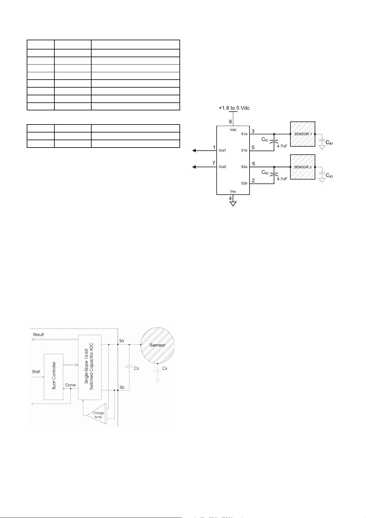
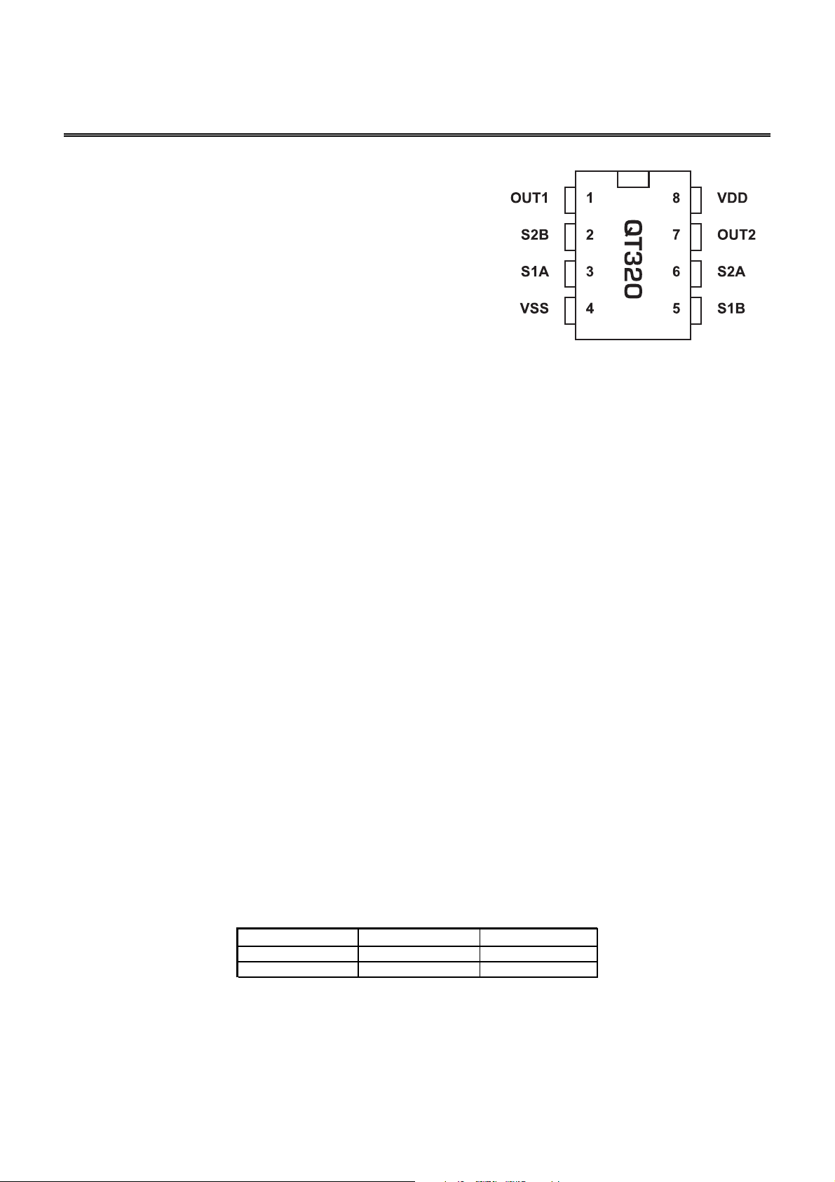
Table 1-1 Pin Descriptions
FunctionNamePin
Detection output, Ch. 1OUT11
Sense Ch 2 pin BS2B2
Sense Ch 1 pin AS1A3
Negative supply (ground)VSS4
Sense Ch 1 pin BS1B5
Sense Ch 2 pin AS2A6
Detection output, Ch. 2OUT27
Positive supplyVDD8
Alternate Pin Functions for Cloning
Serial clone data clockSCK3
Serial clone data outSDO6
Serial clone data inSDI7
1 - OVERVIEW
The QT320 is a 2 channel digital burst mode charge-transfer
(QT) sensor designed specifically for touch controls; it
includes all hardware and signal processing functions
necessary to provide stable sensing under a wide variety of
changing conditions. Only two low-cost, non-critical capacitors
are required for operation.
A unique aspect of the QT320 is the ability of the designer to
‘clone’ a wide range of user-defined setups into the part’s
eeprom during development and in production. Cloned setups
can dramatically alter the behavior of each channel,
independently. For production, the parts can be cloned
in-circuit or can be procured from Quantum pre-cloned.
Figure 1-1 shows the basic QT320 circuit using the device,
with a conventional output drive and power supply
connections.
1.1 BASIC OPERATION
The QT320 employs bursts of variable-length charge-transfer
cycles to acquire its signal. Burst mode permits power
consumption in the microamp range, dramatically reduces RF
emissions, lowers susceptibility to EMI, and yet permits
excellent response time. Internally the signals are digitally
processed to reject impulse noise using a 'consensus' filter
Figure 1-2 Internal Switching
which requires several consecutive confirmations of a
detection before an output is activated.
The two channels of sensing operate in a completely
independent fashion. A unique cloning process allows the
internal eeprom of the device to be programmed for each
channel, to permit unique combinations of sensing and
processing functions for each.
The two sensing channels operate in interleaved
time-sequence and thus cannot interfere with each other.
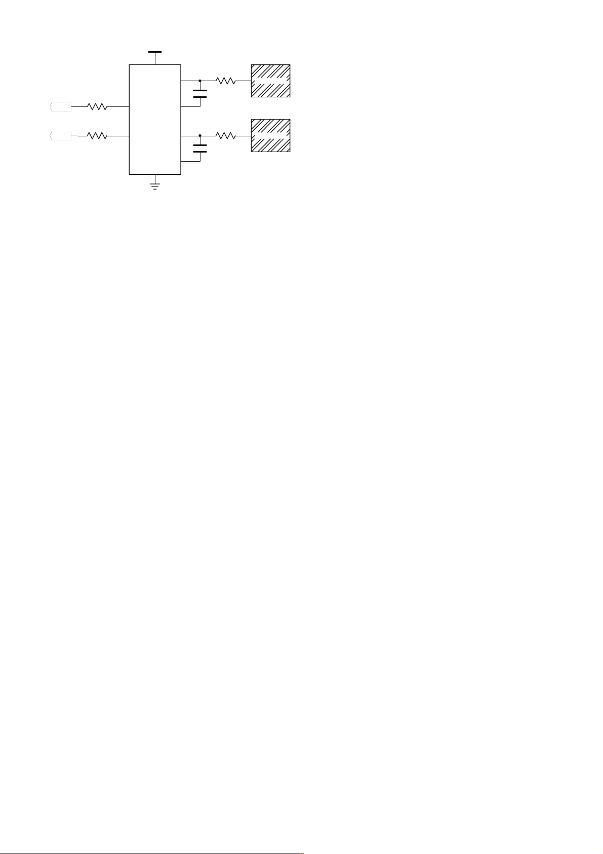
Figure 1-1 Basic QT320 circuit
1.2 ELECTRODE DRIVE
1.2.1 S
The IC implements two channels of direct-to-digital
capacitance acquisition using the charge-transfer method, in
a process that is better understood as a capacitanceto-digital converter (CDC). The QT switches and charge
measurement functions are all internal to the IC (Figure 1-2).
The CDC treats sampling capacitor Cs as a floating store of
accumulated charge which is switched between the sense
pins; as a result, the sense electrode can be connected to
either pin with no performance difference. In both cases the
rule Cs >> Cx must be observed for proper operation. The
polarity of the charge build-up across Cs during a burst is the
same in either case. Typical values of Cs range from 2nF to
100nF for touch operation.
Larger values of Cx cause charge to be transferred into Cs
more rapidly, reducing available resolution and resulting in
lower gain. Conversely, larger values of Cs reduce the rise of
differential voltage across it, increasing available resolution
and raising gain. The value of Cs can thus be increased to
allow larger values of Cx to be tolerated (Figures 5-1 to 5-4).
As Cx increases, the length of the burst decreases resulting in
lower signal numbers.
It is possible to connect separate Cx and Cx’ loads to Sa and
Sb simultaneously, although the result is no different than if
the loads were connected together at Sa (or Sb). It is
important to limit the amount of stray Cx capacitance on both
terminals, especially if the load Cx is already large. This can
be accomplished by minimising trace lengths and widths.
WITCHING OPERATION
lQ
2 QT320/R1.03 08/02
1.2.2 C
f
f
The PCB traces, wiring, and any components associated with
or in contact with Sa and Sb of either channel will become
touch sensitive and should be treated with caution to limit the
touch area to the desired location.
Multiple touch electrodes can be connected to one sensing
channel, for example to create a control button on both sides
of an object, however it is impossible for the sensor to
distinguish between the two connected touch areas.
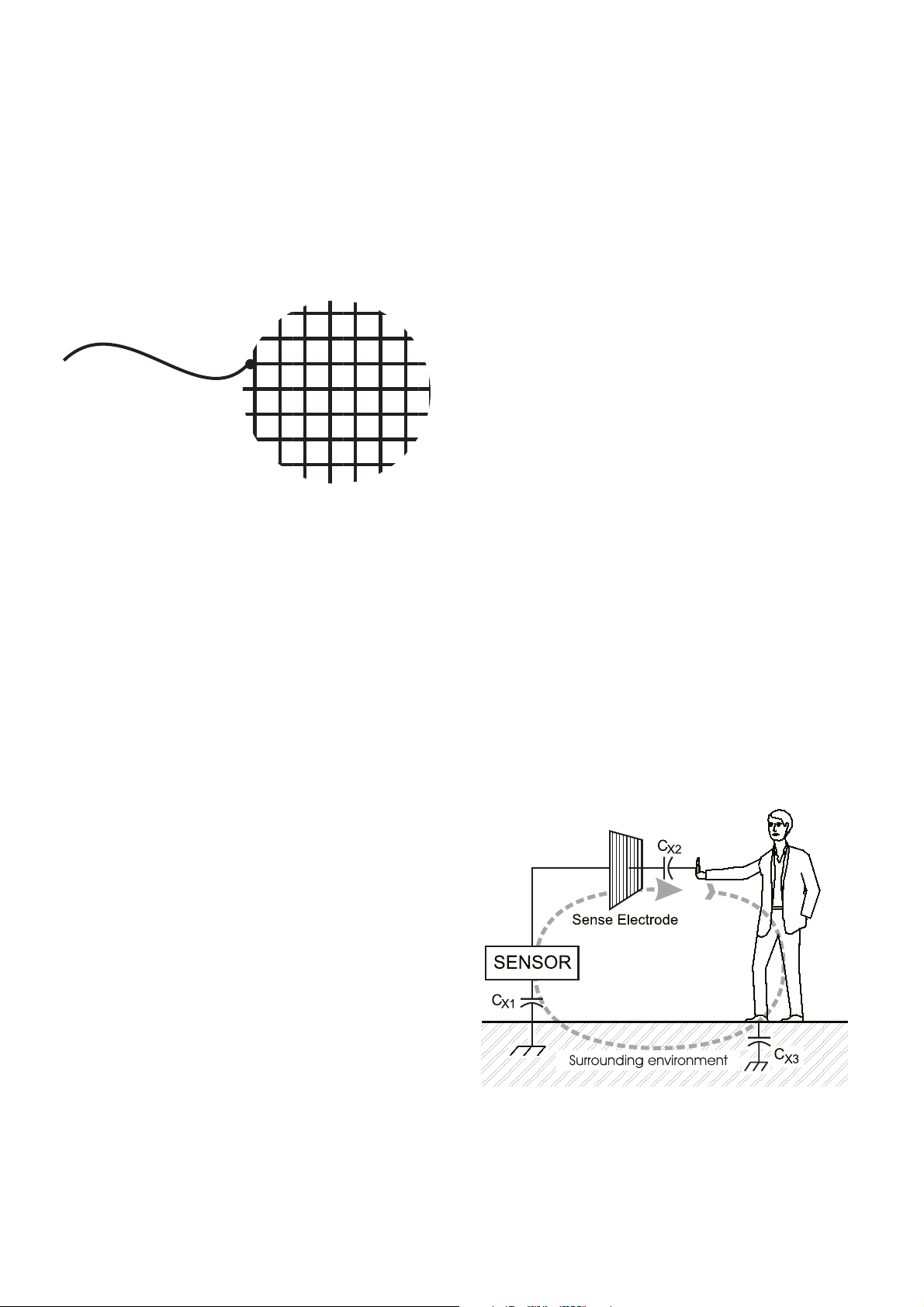
ONNECTION TO ELECTRODES
Figure 1-3 Mesh Electrode Geometry
1.3.2 K
Like all capacitance sensors, the QT320 relies on Kirchoff’s
Current Law (Figure 1-4) to detect the change in capacitance
of the electrode. This law as applied to capacitive sensing
requires that the sensor’s field current must complete a loop,
returning back to its source in order for capacitance to be
sensed. Although most designers relate to Kirchoff’s law with
regard to hardwired circuits, it applies equally to capacitive
field flows. By implication it requires that the signal ground
and the target object must both be coupled together in some
manner in order for the sensor to operate properly. Note that
there is no need to provide an actual hardwired ground
connection; capacitive coupling to ground (Cx1) often is
sufficient, even if the coupling might seem very tenuous. For
example, powering the sensor via an isolated transformer will
almost always provide ample ground coupling, since there is
plenty of capacitance between the primary and secondary
windings via the transformer core and from there to the power
wiring itself directly to 'local earth'. Even when battery
powered, just the physical size of the PCB and the object into
which the electronics is embedded is often enough to couple
enough back to local earth.
The implications of Kirchoff’s law can be most visibly
demonstrated by observing the E3B eval board’s sensitivity
change between laying the board on a table versus holding
the board in your hand by it’s batteries. The effect can also be
observed by holding the board only by one electrode, letting it
recalibrate, then touching the battery end; the board will work
quite well in this mode.
IRCHOFF’S CURRENT LAW
1.2.3 B
The acquisition process occurs in bursts (Figure 1-7) of
variable length, in accordance with the single-slope CDC
method. The burst length depends on the values of Cs and
Cx. Longer burst lengths result in higher gains and more
sensitivity for a given threshold setting, but consume more
average power and are slower.
Burst mode operation acts to lower average power while
providing a great deal of signal averaging inherent in the CDC
process, making the signal acquisition process more robust.
The QT method is a very low impedance method of sensing
as it loads Cx directly into a very large capacitor (Cs). This
results in very low levels of RF susceptibility.
URST MODE OPERATION
1.3 ELECTRODE DESIGN
1.3.1 E
There is no restriction on the shape of the electrodes; in most
cases common sense and a little experimentation can result
in a good electrode design. The QT320 will operate equally
well with long, thin electrodes as with round or square ones;
even random shapes are acceptable. The electrode can also
be a 3-dimensional surface or object. Sensitivity is related to
electrode surface area, orientation with respect to the object
being sensed, object composition, and the ground coupling
quality of both the sensor circuit and the sensed object.
Smaller electrodes will have less sensitivity than large ones.
If a relatively large electrode surfaces are desired, and if tests
show that an electrode has a high Cx capacitance that
reduces the sensitivity or prevents proper operation, the
electrode can be made into a mesh (Figure 1-3) which will
have a lower Cx than a solid electrode area.
LECTRODE GEOMETRY AND SIZE
1.3.3 V
When detecting human contact (e.g. a fingertip), grounding of
the person is never required, nor is it necessary to touch an
exposed metal electrode. The human body naturally has
several hundred picofarads of ‘free space’ capacitance to the
local environment (Cx3 in Figure 1-4), which is more than two
orders of magnitude greater than that required to create a
return path to the QT320 via earth. The QT320's PCB
however can be physically quite small, so there may be little
‘free space’ coupling (Cx1 in Figure 1-4) between it and the
environment to complete the return path. If the QT320 circuit
ground cannot be grounded via the supply connections, then
IRTUAL CAPACITIVE GROUNDS
Figure 1-4 Kircho
’s Current Law
lQ
3 QT320/R1.03 08/02
Sen se
wire
Unshielded
Electrode
Sense
wire
Shielded
Electro de
Figure 1-5 Field Shielding & Shaping
a ‘virtual capacitive ground’ may be required to increase
return coupling.
A ‘virtual capacitive ground’ can be created by connecting the
QT320’s own circuit ground to:
(1) A nearby piece of metal or metallized housing;
(2) A floating conductive ground plane;
(3) A fastener to a supporting structure;
(4) A larger electronic device (to which its output might be
connected anyway).
Because the QT320 operates at a relatively low frequency,
about 500kHz, even long inductive wiring back to ground will
usually work fine.
Free-floating ground planes such as metal foils should
maximise exposed surface area in a flat plane if possible. A
square of metal foil will have little effect if it is rolled up or
crumpled into a ball. Virtual ground planes are more effective
and can be made smaller if they are physically bonded to
other surfaces, for example a wall or floor.
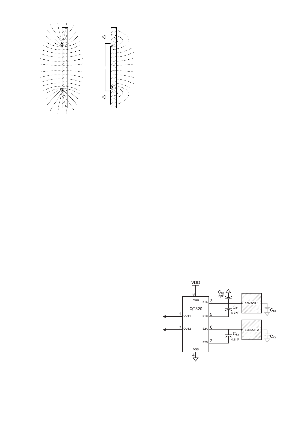
1.3.4 F
IELD SHIELDING AND SHAPING
The electrode can be prevented from sensing in undesired
directions with the assistance of metal shielding connected to
circuit ground (Figure 1-5). For example, on flat surfaces, the
field can spread laterally and create a larger touch area than
desired. To stop field spreading, it is only necessary to
surround the touch electrode on all sides with a ring of metal
connected to circuit ground; the ring can be on the same or
opposite side from the electrode. The ring will kill field
spreading from that point outwards.
If one side of the panel to which the electrode is fixed has
moving traffic near it, these objects can cause inadvertent
detections. This is called ‘walk-by’ and is caused by the fact
that the fields radiate from either surface of the electrode
equally well. Again, shielding in the form of a metal sheet or
foil connected to circuit ground will prevent walk-by; putting a
small air gap between the grounded shield and the electrode
will keep the value of Cx lower and is encouraged. In the case
of the QT320, sensitivity can be high enough (depending on
Cx and Cs) that 'walk-by' signals are a concern; if this is a
problem, then some form of rear shielding may be required.
1.4 SENSITIVITY ADJUSTMENTS
There are three variables which influence sensitivity
independently for each channel:
1. Cs (sampling capacitor)
2. Cx (unknown capacitance)
3. Signal threshold value
There is also a sensitivity dependence of the whole device on
Vdd. Cs and Cx effects are covered in Section 1.2.1.
The threshold setting can be adjusted independently for each
channel from 1 to 16 counts of signal swing (Section 2.2).
Note that sensitivity is also a function of other things like
electrode size, shape, and orientation, the composition and
aspect of the object to be sensed, the thickness and
composition of any overlaying panel material, and the degree
of mutual coupling of the sensor circuit and the object (usually
via the local environment, or an actual galvanic connection).
It is advisable to set the sensitivity to the approximate desired
result by changing Cx and Cs first using a signal threshold
fixed at 10. Use the threshold value thereafter to fine-tune
sensitivity.
1.4.1 I
In some cases it may be desirable to greatly increase
sensitivity, for example when using the sensor with very thick
panels having a low dielectric constant, or when sensing low
capacitance objects.
Sensitivity can be increased by using a bigger electrode,
reducing panel thickness, or altering panel composition.
Increasing electrode size can have diminishing returns, as
high values of Cx load will also reduce sensor gain (Figures
5-1 to 5-4). The value of Cs also has a dramatic effect on
sensitivity, and this can be increased in value up to a limit.
Increasing electrode surface area will not substantially
increase sensitivity if its area is already larger than the object
to be detected. The panel or other intervening material can be
made thinner, but again there are diminishing rewards for
doing so. Panel material can also be changed to one having a
higher dielectric constant, which will help propagate the field.
Locally adding some conductive material to the panel
(conductive materials essentially have an infinite dielectric
constant) will also help; for example, adding carbon or metal
fibers to a plastic panel will greatly increase frontal field
NCREASING SENSITIVITY
Figure 1-6 Circuit with Csx gain equalization capacitor
lQ
4 QT320/R1.03 08/02
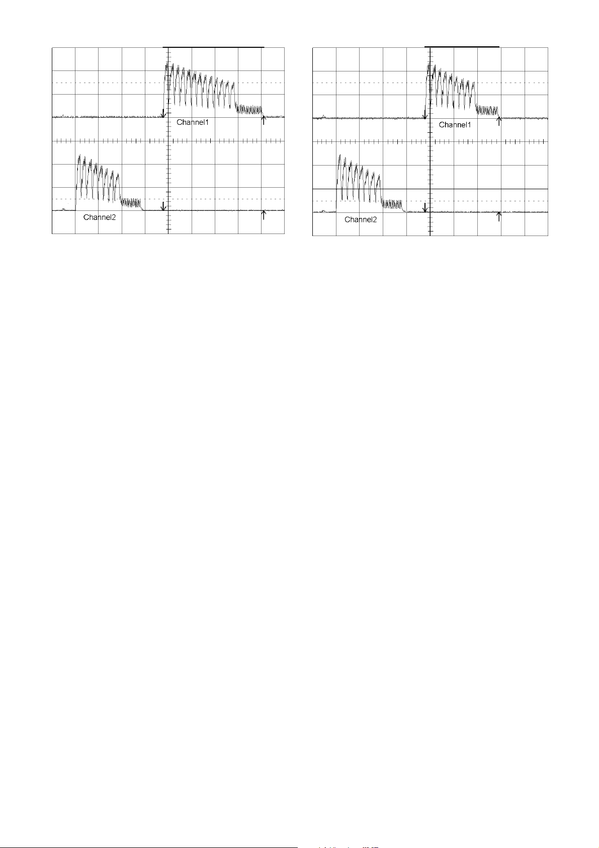
Figure 1-7 Burst lengths without Csx installed
(observed using a 750K resistor in series with probe)
Figure 1-8 Burst lengths with Csx installed
(observed using a 750K resistor in series with probe)
strength, even if the fiber density is too low to make the
plastic electrically conductive.
1.4.2 D
In some cases the circuit may be too sensitive, even with high
signal threshold values. In this case gain can be lowered by
making the electrode smaller, using sparse mesh with a high
space-to-conductor ratio (Figure 1-3), and most importantly by
decreasing Cs. Adding Cx capacitance will also decrease
sensitivity.
It is also possible to reduce sensitivity by making a capacitive
divider with Cx by adding a low-value capacitor in series with
the electrode wire.
1.4.3 H
Hysteresis is required to prevent chattering of the output lines
with weak, noisy, or slow-moving signals.
The hysteresis can be set independently per channel.
Hysteresis is a reference-based number; thus, a threshold of
10 with a hysteresis of 2 will yield 2 counts of hysteresis
(20%); the channel will become active when the signal equals
or exceeds a count of 10, and go inactive when the count falls
to 7 or lower.
Hysteresis can also be set to zero (0), in which case the
sensor will go inactive when the count falls to 9 or lower in the
above example.
Threshold levels of under 4 counts are hard to deal with as
the hysteresis level is difficult to set properly.
1.4.4 C
Channel 1 has less internal Cx than Channel 2, which makes
it more sensitive than Channel 2 given equal Cx loads and Cs
ECREASING SENSITIVITY
YSTERESIS
HANNEL BALANCE
capacitors. This can be useful in some designs where one
more sensitive channel is desired, but if equal sensitivity is
required a few basic rules should be followed:
1. Use a symmetrical PCB layout for both channels: Place
the IC half way between the two electrodes to match Cx
loading. Avoid routing ground plane (or other traces) close
to either sense line or the electrodes; allow 4-5 mm
clearance from any ground or other signal line to the
electrodes or their wiring. Where ground plane is required
(for example, under and around the QT320 itself) the
sense wires should have minimized adjacency to ground.
2. Connect a small capacitor (~5pF) between S1a or S1b
(either Channel 1 pin) and circuit ground (Csx in Figure
1-6), this will increase the load capacitance of Channel 1,
thus balancing the sensitivity of the two channels (see
Figures 1-7, 1-8).
3. Adjust Cs and/or the internal threshold of the two channels
until the sensitivities of the two channels are
indistinguishable from each other.
Since the actual burst length is proportional to sensitivity, you
can use an oscilloscope to balance the two channels with
more accuracy than by empirical methods (See Figures 1-7
and 1-8). Connect one scope probe to Channel 1 and the
other to Channel 2, via large resistors (750K ohms) to avoid
disturbing the measurement too much, or, use a low-C FET
probe. The Csx balance capacitor should be adjusted so that
the burst lengths of Channels 1 and 2 look nearly the same.
With some diligence the PCB can also be designed to include
some ground plane nearer to Channel 1 traces to induce
about 5pF of Csx load without requiring an actual discrete
capacitor.
lQ
5 QT320/R1.03 08/02
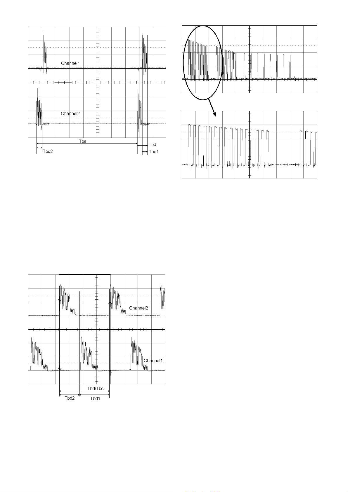
Figure 1-9 Bursts when SC > 0
1.5 TIMING
The QT320 runs two sensing bursts, one per channel, each
acquisition cycle (Figure 1-9). The bursts are successive in
time, with Channel 2 firing first.
The basic QT320 timing parameters are:
Ti Basic timing interval (1.5.1)
Tbs Burst spacing (1.5.1)
Tbd1 Burst duration, Channel 1 (1.5.2)
Tbd2 Burst duration, Channel 2 (1.5.2)
Tbd Burst duration, Ch1 + Ch2 (1.5.2)
Tmod Max On-Duration (1.5.3)
Tdet Detection response time (1.5.4)
Figure 1-11 Burst detail
1.5.1 B
Between acquisition bursts, the device can go into a low
power sleep mode. The percentage of time spent in sleep
depends on the burst spacing and the combined burst lengths
of both channels; if the burst lengths occupy all of the sleep
interval, no time will be spent in sleep mode and the part will
operate at maximum power drain.
The burst spacing is a multiple of the basic timing interval Ti;
Ti in turn depends heavily on Vdd (see Section 2.1 and Figure
5.7). The parameter ‘Sleep Cycles’ or SC is the user-defined
Setup value which controls how many Ti intervals there are
from the start of a burst on Channel 2 until the start of the
next such burst. The resulting timing is Tbs:
All the basic timing parameters of the QT320 such as
recalibration delay etc. are dependent on Tbs.
If SC = 0, the device never sleeps between bursts (Figure
1-10). This mode is fast but consumes maximum power; it is
also unregulated in timing from burst to burst, depending on
the combined burst lengths of both channels.
Conversely if SC >> 0, the device will spend most of its time
in sleep mode and will consume very little power, but it will be
slower to respond.
By selecting a supply voltage and a value for SC, it is possible
to fine-tune the circuit for the desired speed / power tradeoff.
URST SPACING
Tbs = SC x Ti where SC > 0.
: TI, SC, T
BS
Figure 1-10 Bursts when SC = 0
(750K resistor in series with scope probe)
lQ
1.5.2 B
The two burst durations depend entirely on the values of Cs
and Cx for the coresponding sensing channel, and to a lesser
extend, Vdd. The bursts are composed of hundreds of
charge-transfer cycles (Figure 1-11) operating at about
500kHz. Channel 2 always fires first (Tbd2) followed by
Channel 1 (Tbd1); the sum total of the time required by both
channels is parameter Tbd.
URST DURATIONS
: TBD1, TBD2, T
BD
6 QT320/R1.03 08/02

When SC=0 (no sleep cycles), the sensor operates without a
fixed timing and the acquisition spacing Tbs is the sum of the
burst durations for both channels (Figure 1-10). In this mode
of operation, Tbs and Tbd are the same value.
1.5.3 MAX ON-D
The Max On-Duration is the amount of time required for a
continuously detecting sense channel to recalibrate itself. This
parameter is user settable by changing MOD and SC (Section
2.6).
Tmod restarts if the OUT pin becomes inactive.
A recalibration of one channel has no effect on the other;
Tmod operates independently for each channel.
1.5.4 R
Response time from the onset of detection to an actual OUT
pin becoming active depends on:
Ti depends in turn on Vdd.
If the control bit DIS is normal (0), then Tdet depends on the
rate at which the bursts are acquiring, and the value of DIT. A
DIT number of bursts must confirm the detection before the
OUT line becomes active:
If DIS is set to fast, then Tdet also depends on BL:
Ti depends in turn on Vdd; Tbd depends on Cs and Cx for
both channels.
Quantum’s QT3View software calculates an estimate of
response time based on these parameters.
ESPONSE TIME
Ti Basic Timing Interval
SC Sleep Cycles (user setting)
DIT Detection Integrator Target (user setting)
DIS Detect Integration Speed (user setting)
Tbd Burst duration (if DIS is set too fast)
Tdet = SC x Ti x DIT (normal DIS)
Tdet = (SC x Ti) + (DIT-1)*Tbd (fast DIS)
URATION
, T
, T
DET
MOD
1.6 EXTERNAL RECALIBRATION
The QT320 has no recalibration pin; a forced recalibration is
accomplished only when the device is powered up. However,
supply drain is low enough that the IC can be powered from a
logic gate or I/O pin of an MCU; driving the Vdd pin low and
high again can serve as a forced recalibration. The source
resistance of many CMOS gates and MCU’s are
low enough to provide direct power without
problems. A 0.01uF minimum bypass capacitor is
required directly across Vdd to Vss.
2 - CONTROL & PROCESSING
All acquisition functions are digitally controlled and can be
altered via the cloning process.
Signals are processed using 16 bit integers, using
Quantum-pioneered algorithms specifically designed to
provide for high survivability.
2.1 SLEEP CYCLES (SC)
Range: 0..255; Default: 1
Affects speed & power of entire device.
Refer to Section 1.5.1 for more information on the effect of
Sleep Cycles.
SC changes the number of intervals Ti separating two
consecutive burst pairs (Figure 1-10). SC = 0 disables sleep
intervals and bursts are crowded together with a rep rate that
depends entirely on the burst lengths of both channels
(Section 1.5.2).
Response time, drift compensation rate, max on-duration, and
power consumption are all affected by this parameter. A high
value of SC will make the sensor very low power and very
slow.
2.2 DRIFT COMPENSATION (PDC, NDC)
Signal drift can occur because of changes in Cx, Cs, Vdd,
electrode contamination and aging effects. It is important to
compensate for drift, otherwise false detections and sensitivity
shifts can occur.
Drift compensation is performed by making the signal’s
reference level slowly track the raw signal while no detection
is in effect. The rate of adjustment must be performed slowly,
otherwise legitimate detections could be affected. The device
compensates using a slew-rate limited change to the signal
reference level; the threshold and hysteresis points are slaved
to this reference.
Once an object is detected, drift compensation stops since a
legitimate signal should not cause the reference to change.
Positive and negative drift compensation rates (PDC, NDC)
can be set to different values (Figure 2-1). This is invaluable
for permitting a more rapid reference recovery after a channel
has recalibrated while an object was present and then
removed.
lQ
Figure 2-1 Drift Compensation
7 QT320/R1.03 08/02

If SC > 0, then PDC+1 sets the number of burst spacings,
Tbs, that determines the interval of drift compensation, where:
Tbs = SC x Ti (Section 1.5.1)
Example: PDC = 9, (user setting)
Tbs = 100ms
then
Tpdc = (9+1) x 100ms = 1 sec.
If SC = 0, the result is multplied by 16, and Tbd becomes the
time basis for the compensation rate, where:
Tbd = Tbd1 + Tbd2 (Section 1.5.2)
Example: PDC = 5, (user setting)
Tbd = 31ms
then
Tpdc = (5+1) x 31ms x 16 = 2.98 sec
NDC operates in exactly the same way as PDC.
2.2.1 P
Range: 0..255; Default: 100; 255 disables
Ability to compensate for drift with increasing signals.
PDC corrects the reference when the signal is drifting up.
Every interval of time the device checks each channel for the
need to move its reference level in the positive direction in
accordance with signal drift. The resulting timing interval for
this adjustment is Tpdc.
This value should not be set too fast, since an approaching
finger could be compensated for partially or entirely before
even touching the sense electrode. Tpdc is common to both
sensing channels and cannot be independently adjusted.
2.2.2 N
Range: 0...255 Default: 2; 255 disables
Aability to compensate for drift with decreasing signals.
This corrects the reference level when the signal is
decreasing due to signal drift. This should normally be faster
than positive drift compensation in order to compensate
quickly for the removal of a touch or obstruction from the
electrode after a MOD
recalibration (Section 1.5.3).
This parameter is common to
both channels. The resulting
timing interval for this
adjustment is Tndc.
OSITIVE DRIFT COMPENSATION
EGATIVE DRIFT COMPENSATION
(PDC)
(NDC)
2.3 THRESHOLDS (THR1, THR2)
Range: 1..16; Default: 6
Affects sensitivity.
The detection threshold is set independently for each channel
via the cloning process. Threshold is measured in terms of
counts of signal deviation with respect to the reference level.
Higher threshold counts equate to less sensitivity since the
signal must travel further in order to cross the detection point.
If the signal equals or exceeds the threshold value, a
detection can occur. The detection will end only when the
signal become less than the hysteresis level.
2.4 HYSTERESIS (HYS1, HYS2)
Range: 0...16; Default: 2
Affects detection stability.
The hysteresis levels are set independently for each channel
via the cloning process. Hysteresis is measured in terms of
counts of signal deviation below the threshold level. Higher
values equate to more hysteresis. The channel will become
inactive after a detection when the signal level falls below
THRn-HYSn. Hysteresis prevents chattering of the OUT pin
when there is noise present.
If HYS1 or HYS2 are set to a value equal or greater than
THR1 or THR2 respectively, the channel may malfunction.
Hysteresis should be set to between 10% and 40% of the
threshold value for best results.
If THR1 = 10 and HYS1 = 2, the hysteresis zone will represent
20% of the threshold level. In this example the ‘hysteresis
zone’ is the region from 8 to 10 counts of signal level. Only
when the signal falls back to 7 will the OUT pin become
inactive.
lQ
Figure 2-2 Detect Integrator Filter Operation
8 QT320/R1.03 08/02

2.5 DETECT INTEGRATORS (DIA, DIB, DIS)
DIAT1, 2 Range: 1..256 Default: 10
DIBT1, 2 Range: 1..6 Default: 6
DIS Range: 0, 1 Default: 1
Affects response time Tdet.
See Figure 2-2 for operation.
It is usually desirable to suppress detections generated by
sporadic electrical noise or from quick contact with an object.
To accomplish this, the QT320 incorporates two detection
integrator (‘DI’) counters per channel that serve to confirm
detections and slow down response time. The counter pairs
operate independently for each sensing channel.
DIA / DIAT: The first counter, DIA, increments after each
burst if the signal threshold has been exceeded in that burst,
until DIA reaches its terminal count DIAT, after which the
corresponding OUT pin goes active. If the signal falls below
the threshold level prior to reaching DIAT, DIA resets.
DIA can also be viewed as a 'consensus' filter that requires
signal threshold crossings over ‘T’ successive bursts to create
an output, where ‘T’ is the terminal count (DIAT).
DIA1 / DIAT1 and DIA2 / DIAT2 are used in conjunction with
their respective channels.
DIB / DIBT: If OUT is active and the signal falls below the
hysteresis level, detect integrator DIB, counts up towards
terminal count DIBT; when DIBT is reached, OUT is
deactivated. DIBT is the same as DIAT if DIBT <= 6;
If DIAT > 6, then DIBT = 6.
DIBT cannot be adjusted separately from DIAT.
DIS: Because the DI counters count at the burst rate, slow
burst spacings can result in very long detection delays with
terminal counts above 1. To cure this problem, the burst rate
can be made faster while DIA or DIB is counting up. This
creates the effect of a gear-shifted detection process: normal
speed when there are no threshold crossings, and fast mode
when a detection is pending. The control bit for the fast DI
mode is referred to as DIS. DIS applies to both channels; it
cannot be enabled for just one channel.
DIS gear-shifts the effect of both DIA and DIB. The
gear-shifting ceases and normal speed resumes once the
detection is confirmed (DIA = DIAT) and once the detection
ceases (DIB = DIBT).
When SC=0 the device operates without any sleep cycles,
and so the timebase for the DI counters is very fast.
The MOD function can also be disabled, in which case the
channel will never recalibrate unless the part is powered down
and back up again. In infinite timeout the designer should
take care to ensure that drift in Cs, Cx, and Vdd do not cause
the device to ‘stick on’ inadvertently when the target object is
removed from the sense field.
MOD is expressed in multiples of the burst space interval,
which can be either Tbs or Tbd depending on the Sleep
Cycles setting (SC).
If SC > 0, the delay is:
Tmod = (MOD + 1) x 16 x Tbs
Example:
Tbs = 100ms,
MOD = 9;
Tmod = (9 + 1) x 16 x 100ms = 160 secs.
If SC = 0, Tmod is a function of the total combined burst
durations, Tbd. If SC = 0, the delay is:
Tmod = (MOD + 1) x 256 x Tbd
Example:
Tbd = 18ms,
MOD = 9;
Tmod = (9 + 1) x 256 x 18ms = 46 secs.
If MOD = 255, recalibration timeout = infinite (disabled)
regardless of SC.
An MOD induced recalibration will make an OUT pin inactive
except if the output is set to toggle mode (Section 2.7.2), in
which case the OUT state will be unaffected but the
underlying channel will have recalibrated.
2.7 OUTPUT FEATURES
Available output processing options accommodate most
requirements; these can be set via the clone process.
Both OUT pins are open-drain, and require pullup resistors.
2.7.1 DC M
In DC mode the OUT pins respond to detections with a
steady-state active logic level, this state will endure for the
length of time that a detection exists or until a MOD timeout
occurs (Section 2.6).
The polarity of OUT can be set via the cloning process. Each
channel can be set for this feature independently. Either
active-low or active-high can be selected.
ODE
, P
OLARITY
2.6 MAX ON-DURATION (MOD)
Range: 0..255; Default: 14; 255 disables
Affects parameter Tmod, the calibration delay time
If a stray object remains on or near the sense electrode, the
signal may rise enough to activate an OUT pin thus
preventing normal operation. To provide a way around this, a
Max On-Duration (‘MOD’) timer is provided to cause a
channel recalibration if the activation lasts longer than the
designated timeout, Tmod.
The timeout applies individually per channel. If one channel is
active for the Max On-duration interval it will recalibrate, but
the other channel will remain unaffected.
lQ
2.7.2 T
Toggle mode gives OUT pins a touch-on / touch-off flip-flop
action, so that its state changes with each detection. It is most
useful for controlling power loads, for example kitchen
appliances, power tools, light switches, etc.
MOD time-outs (Section 2.6) will recalibrate the underlying
channel but leave the OUT state unchanged.
OUT polarity (Section 2.7.1) has no effect when toggle mode
is engaged. The initial state at power-up of the OUT pins in
toggle mode is always open drain (logic high).
Each channel can be set individually for this feature.
OGGLE MODE
9 QT320/R1.03 08/02
Vdd
8
OUT1
OUT2
RE3
RE4
VDD
1
OUT1
7
OUT2 S2A
VSS
4
S1A
S1B
S2B
3
5
6
2
Figure 3-1 ESD/EMC protection resistors
CS1
CS2
RE1
RE2
SENSOR 1
SENSOR 2
3.2 POWER SUPPLY
3.2.1 S
The QT320 derives its internal references from the power
supply. Sensitivity shifts and timing changes will occur with
changes in Vdd, as often happens when additional power
supply loads are switched on or off via one of the Out pins.
These supply shifts can induce detection ‘cycling’, whereby
an object is detected, the load is turned on, the supply sags,
the detection is no longer sensed, the load is turned off, the
supply rises and the object is reacquired, ad infinitum.
Detection ‘stiction’, the opposite effect, can occur if a load is
shed when an output is active and the signal swings are
small: the Out pin can remain stuck even if the detected
object is no longer near the electrode.
TABILITY
2.7.3 H
EARTBEAT
™ O
UTPUT
Both OUT pins have HeartBeat™ ‘health’ indicator pulses
superimposed on them. Heartbeat floats both 'OUT' pins for
approximately 15µs once before Channel 2’s burst.
These pulses can be used to determine that the sensor is
operating properly. The pulses are evident on an OUT line
that is low, and appear as positive pulses.
They are not evident on an OUT pin that is high.
Heartbeat indication can be used to determine if the chip is
operating properly. The frequency of the pulses can be used
to determine if the IC is operating within desired limits.
It is not possible to disable these pulses.
Heartbeat pulses can be easily filtered by placing a suitable
capacitor from an OUT pin to Vss, to prevent the OUT line
from rising substantially within the 15µs pulse. For example,
with a 10K pullup resistor, the capacitor can be 0.015µF of
virtually any type.
2.7.4 O
UTPUT DRIVE CAPABILITY
The outputs can sink up to 2mA of non-inductive current. If an
inductive load is used, such as a small relay, the load should
be diode-clamped to prevent damage. The current must be
limited to 2mA max to prevent detection side effects from
occurring, which happens when the load current creates
voltage drops on the die and bonding wires; these small shifts
can materially influence the signal level to cause detection
instability.
3 CIRCUIT GUIDELINES
3.1 SAMPLE CAPACITORS
Cs capacitors can be virtually any plastic film or low to
medium-K ceramic capacitor. The normal usable Cs range is
from 1nF ~ 200nF depending on the sensitivity required;
larger values of Cs require higher stability to ensure reliable
sensing. Acceptable capacitor types include NPO or C0G
ceramic, PPS film, Y5E and X7R ceramic in that order.
If the design requires sensitivity matching between channels,
it is strongly advised to use tight tolerance capacitors and to
trim the relative sensitivities as described in Section 1.4.4.
3.2.2 S
UPPLY REQUIREMENTS
Vdd can range from 1.8 to 5.25 volts during operation, and
2.2 to 5.25 during eeprom Setups configuration. Current drain
will vary depending on Vdd, the chosen sleep cycles, and the
burst lengths. Increasing Cx values will decrease power drain
since increasing Cx loads decrease burst length (Figures 5-1,
5-4).
If the power supply is shared with another electronic system,
care should be taken to assure that the supply is free of
spikes, sags, and surges. The QT320 will track slow changes
in Vdd if drift compensation is enabled, but it can be adversely
affected by rapid voltage steps and spikes at the millivolt
level.
If desired, the supply can be regulated using a conventional
low current regulator, for example CMOS LDO regulators with
low quiescent currents, or standard 78Lxx-series 3-terminal
regulators.
For proper operation a 100nF (0.1uF) ceramic bypass
capacitor should be used between Vdd and Vss; the bypass
cap should be placed very close to the Vdd and Vss pins.
3.3 PCB LAYOUT
3.3.1 G
The use of ground planes around the device is encouraged
for noise reasons, but ground should not be coupled too close
to the four sense pins in order to reduce Cx load. Likewise,
the traces leading from the sense pins to the electrode should
not be placed directly over a ground plane; rather, the ground
plane should be relieved by at least 3 times the width of the
sense traces directly under it, with periodic thin bridges over
the gap to provide ground continuity.
3.3.2 C
If a cloning connector is used, place this close to the QT320
(Figure 4-1). Placing the cloning connector far from the
QT320 will increase the load capacitance Cx of the sensor
and decrease sensitivity, as some of the cloning lines are
sense lines. Long distances on these lines can also make the
clone process more susceptible to communication errors from
ringing and interference.
Cloning can be designed for production by using pads (SMT
or through-hole) on the solder side which are connected to a
fixture via spring loaded ATE-style ‘pogo-pins’. This eliminates
the need for an actual connector to save cost.
ROUND PLANES
LONE PORT CONNECTOR
lQ
10 QT320/R1.03 08/02
3.4 ESD ISSUES
8
S2A
S1A
2
6
3
4
S2B
S1B
5
SCK
OUT2
VSS
7
OUT2
SENSOR 2
SENSOR 1
OUT1
OUT1
1
Vdd
VDD
CS1
GND
SDI
SDO
CS2
In cases where the electrode is placed behind a dielectric
panel, the device will usually be well protected from static
discharge. However, even with a plastic or glass panel,
transients can still flow into the electrode via induction, or in
extreme cases, via dielectric breakdown. Porous materials
may allow a spark to tunnel right through the material;
partially conducting materials like 'pink poly' static dissipative
plastics will conduct the ESD right to the electrode. Panel
seams can permit discharges through edges or cracks.
Testing is required to reveal any problems. The QT320 has
internal diode protection which can absorb and protect the
device from most induced discharges, up to 20mA; the
usefulness of the internal clamping will depend on the
dielectric properties, panel thickness, and rise time of the
ESD transients.
ESD protection can be enhanced with an added resistor as
shown in Figure 3-1. Because the charge and transfer times
of the QT320 are 1us in duration, the circuit can tolerate
values of Re which result in an RC timeconstant of about
200ns. The ‘C’ of the RC is the Cx load on the distant side
from the QT320. Thus, for a Cx load of 20pF, the maximum
Re should be 10K ohms. Larger amounts of Re will result in
an increasingly noticeable loss of sensitivity.
3.5 EMC ISSUES
Electromagnetic and electrostatic susceptibility are often a
problem with capacitive sensors. QT320 behavior under these
conditions can be improved by adding the series-R shown in
Figure 3-1, exactly as shown for ESD protection. The resistor
should be placed next to the chip.
This works because the inbound RC network formed by Re
and Cs has a very low cutoff frequency which can be
computed by the formula:
Fc =
1
2✜ Re Cs
If Re = 10K and Cs = 10nF, then Fc = 1.6kHz.
This leads to very strong suppression of external fields.
Nevertheless, it is always wise to reduce lead lengths by
placing the QT320 as close to the electrodes as possible.
Likewise, RF emissions are sharply curtailed by the use of
Re, which bandwidth limits RF emissions based on the value
of Re and Cx, the electrode capacitance.
Line conducted EMI can be reduced by making sure the
power supply is properly bypassed to chassis ground. The
OUT lines can also be paths for conducted EMI, and these
can be bypassed to circuit ground with an RC filter network.
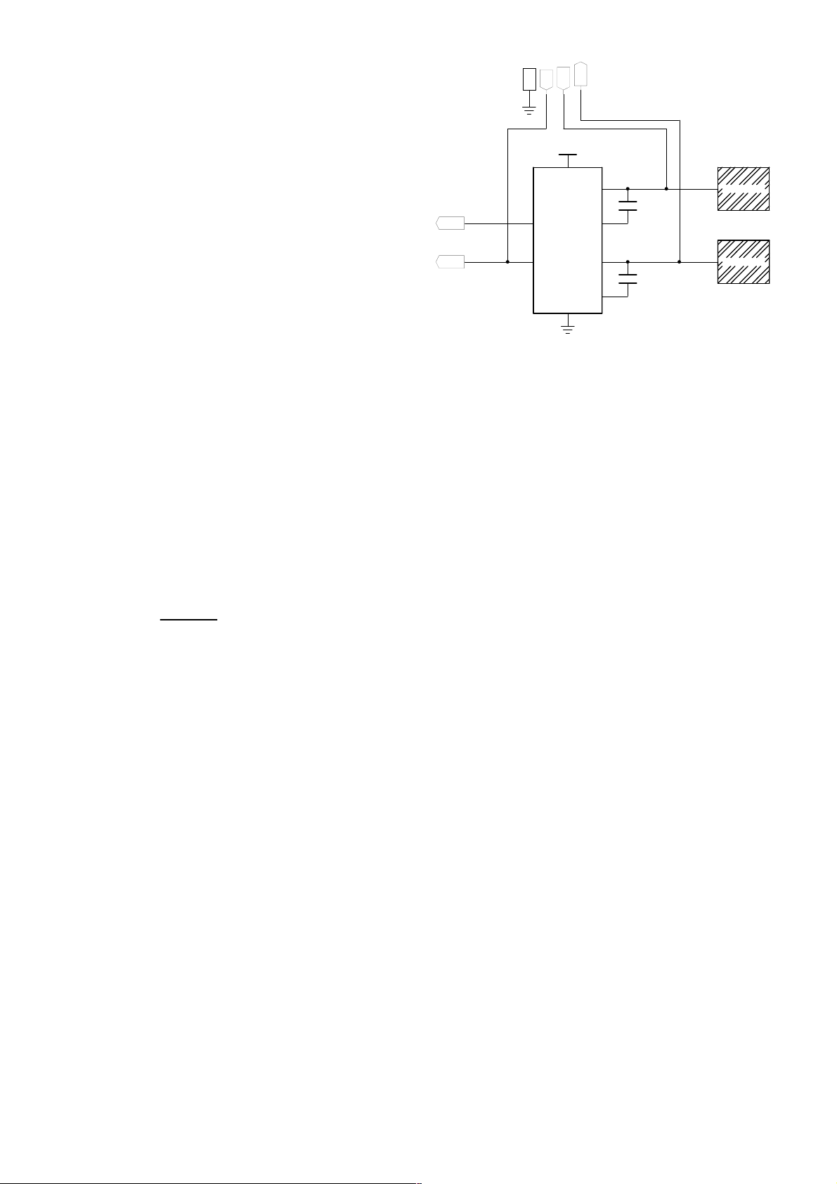
4 PARAMETER CLONING
The cloning process allows user-defined settings to be loaded
into internal eeprom, or read back out, for development and
production purposes.
The QTM300CA cloning board in conjunction with QT3View
software simplifies the cloning process greatly. The E3B eval
Figure 4-1 Clone interface wiring
board has been designed with a connector to facilitate direct
connection with the QTM300CA. The QTM300CA in turn
connects to any PC with a serial port which can run QT3View
software (included with the QTM300CA and available on
Quantum’s web site).
The connections required for cloning are shown in Figure 4-1.
Further information on the cloning process can be found in
the QTM300CA instruction guide. Section 3.3.2 discusses
wiring issues associated with cloning.
The parameters which can be altered are shown in Table 4-1
(next page).
Parameters that can be altered for each channel
independently are:
Threshold
Hysteresis
Detect Integrator A
Detect Integrator B
Max On-Duration
Output Mode
Parameters that are common to the entire part are:
Detect Integrator Speed
Negative Drift Compensation
Positive Drift Compensation
Sleep Cycles
It is possible for an on-board host controller to read and
change the internal settings via the interface, but doing so will
inevitably disturb the sensing process even when data
transfers are not occuring. The additional capacitive loading
of the interface pins will contribute to Cx; also, noise on the
interface lines can cause erratic operation.
The internal eeprom has a life expectancy of 100,000
erase/write cycles.
A serial interface specification for the device can be obtained
by contacting Quantum.
lQ
11 QT320/R1.03 08/02

TABLE 4-1 SETUPS SUMMARY CHART
Det Integrator A
Channel 1
Specific
Channel 2
Specific
Features
Common
To Both
Channels
Note 1: Tbs is the combined (summed) burst duration of Channel1 and Channel2 (Tbd).
Note 2: Tbs is variable with the voltage, see figure 5-7. If Tbd is longer than 10ms,Tbs is Tbd plus the sleep time find on figure 5-7.
Note 5: The sleep period time is find on figure 5-7(equivalent at 1 sleep period).
Det Integrator B
Max-On Duration
Output Mode
Threshold
Hysteresis
DI Speed
Negative Drift
Compensation
Positive Drift
Compensation
Sleep Cycles
MOD1
OUT1
MOD2Max-On Duration
OUT2Output Mode
DIS
NDC
PDC
SC
Finite0 - 254
Active Low 0
Active High1
Toggle2
Finite0 - 254
Active Low 0
Active High 1
Toggle2
Slow0
Fast1
On0 - 254
14 (~10s at 3V)
14 (~10s at 3V)
1
2 (~0.13s/bit
@ 3V)
On0 - 254
No Sleep0
Sleep1 - 255
100 (~4.36s/bit
@ 3V)
1 (~47ms Tbs
@ 3V)
Value taken from DIAT1 but truncated to 66-1 - 6DIBT1
Tmod = (MOD1 + 1) x 256 x Tbs (note1)SC = 0
Tmod = (MOD1 + 1) x 16 x Tbs (note2)SC > 0Infinite255
Requires pullup resistor on OUT10
Value taken from DIAT2 but truncated to 66-1 - 6DIBT2Det Integrator B
Tmod = (MOD2 + 1) x 256 x Tbs (note1)SC = 0
Tmod = (MOD2 +1) x 16 x Tbs (note2)SC > 0Infinite255
Requires pullup resistor on OUT20
Tndc = (NDC + 1) x 16 x Tbs (note1)SC = 0
Tndc = (NDC + 1) x Tbs (note2)SC > 0Off255
Tpdc = (PDC + 1) x 16 x Tbs (note1)SC = 0
Tpdc = (PDC + 1) x Tbs (note2)SC > 0Off255
UnitCalculation / NotesDefaultValid ValuesSymbolDescription
CountsHigher = less sensitive6-1 - 16THR1Threshold
CountsHigher = more hysteresis2-0 - 16HYS1Hysteresis
Burst CyclesHigher = longer to detect, more noise immune10-1 - 256DIAT1
Seconds
-
-
-
CountsHigher = less sensitive6-1 - 16THR2
CountsHigher = more hysteresis2-0 - 16HYS2
Burst CyclesHigher = longer to detect, more noise immune10-1 - 256DIAT2Det Integrator A
Seconds
-
-
-
-
-
-
-
Seconds / bit
change
Seconds / bit
change
CountsBurst rep interval = Tbs = SC x Ti
lQ
12 QT320/R1.03 08/02

5 ELECTRICAL SPECIFICATIONS
5.1 ABSOLUTE MAXIMUM SPECIFICATIONS
Operating temp.................................................................................as designated by suffix
Storage temp........................................................................................ -65
V
DD
...................................................................................................... -0.5 to +6V
Max continuous pin current, any control or drive pin.............................................................. ±40mA
Short circuit duration to ground, any pin..........................................................................infinite
Short circuit duration to V
DD
, any pin.............................................................................infinite
Voltage forced onto any pin................................................................... -0.5V to (Vdd + 0.5) Volts
5.2 RECOMMENDED OPERATING CONDITIONS
VDD..................................................................................................... +1.8 to 5.5V
V
DD
during eeprom writes................................................................................. +2.2 to 5.5V
Short-term supply ripple+noise.................................................................................. ±5mV
Long-term supply stability..................................................................................... ±100mV
Cs value................................................................................................ 1nF to 200nF
Cx value.................................................................................................. 0 to 100pF
5.3 AC SPECIFICATIONS
Vdd = 3.0, Ta = recommended operating range, Cs=100nF unless noted
NotesUnitsMaxTypMinDescriptionSymbol
RC
PC
PT
BL
HB
µs1Charge durationT
µs1Transfer durationT
µs15Heartbeat pulse widthT
Cs, Cx dependentms150Recalibration timeT
Cs = 10nF to 200nF; Cx = 0ms250.5Burst lengthT
O
C to +150OC
5.4 SIGNAL PROCESSING
5.5 DC SPECIFICATIONS
Vdd = 3.0V, Cs = 10nF, Cx = 5pF, Ta = recommended range, unless otherwise noted
DD
DDW
DD
DDS
IL
IH
OL
X
R
V5.251.8Supply voltageV
V5.252.2Vdd during eeprom writeV
pF2000Load capacitance rangeC
bits16Acquisition resolutionA
NotesUnitsMaxTypMinDescriptionSymbol
counts161Threshold differential w.r.t. reference
counts150Hysteresis w.r.t. threshold
samples2561Consensus filter length
ms/bit-Positive drift compensation rate
ms/bit-Negative drift compensation rate
secsinfinite<1Post-detection recalibration timer duration
NotesUnitsMaxTypMinDescriptionSymbol
Depends on setting of Sleep CyclesµA1,50060060Supply currentI
Required for proper start-upV/s100Supply turn-on slopeV
Vdd = 2.5 to 5.0VV0.3 VddInput low voltageV
Vdd = 2.5 to 5.0VV0.6 VddInput high voltageV
OUT1, OUT2, 2mA sinkV0.4Low output voltageV
Threshold = 6; ref. Figure 5-3pF0.4Sensitivity range, Channel 1S1
Threshold = 6; ref. Figure 5-4pF0.6Sensitivity range, Channel 2S2
lQ
13 QT320/R1.03 08/02
10.00
10.00
1.00
0.10
Detection Threshold, pF
0.01
0 1020304050
Cx Load
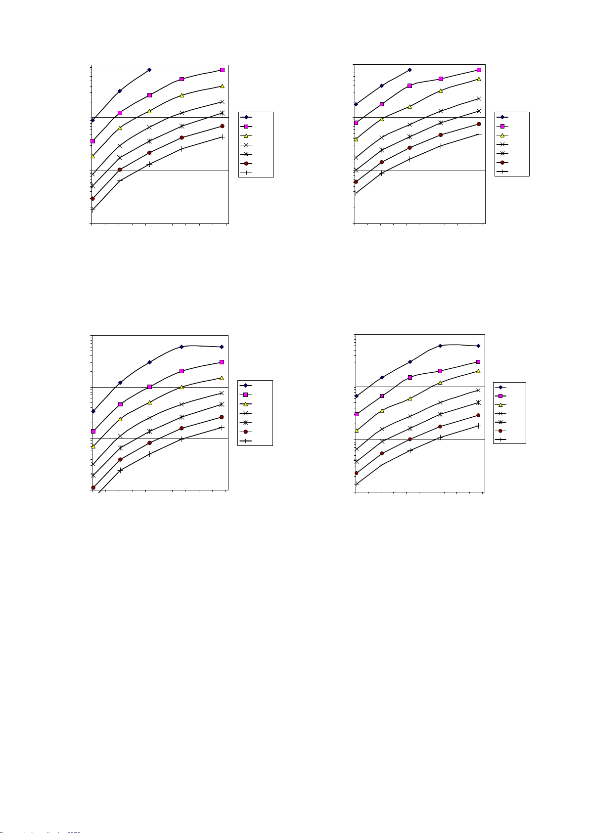
Figure 5-1 Typical Ch 1 Sensitivity vs. Cx;
Threshold = 16, Vdd = 3.0
10.00
1.00
0.10
Detection Threshold, pF
4.7nF
9nF
19nF
43nF
74nF
124nF
200nF
4.7nF
9nF
19nF
43nF
74nF
124nF
200nF
1.00
0.10
Detection Threshold, pF
0.01
0 1020304050
Cx Load
Figure 5-2 Typical Ch 2 Sensitivity vs. Cx;
Threshold = 16, Vdd = 3.0
10.00
1.00
0.10
Detection Threshold, pF
4.5nF
9nF
19nF
43nF
74nF
124nF
200nF
4.7nF
9nF
19nF
43nF
74nF
124nF
200nF
0.01
0 10203040 50
Figure 5-3 Typical Ch 1 Sensitivity vs. Cx;
Threshold = 6, Vdd = 3.0
lQ
Cx Load
0.01
0 1020304050
Cx Load
Figure 5-4 Typical Ch 2 Sensitivity vs. Cx;
Threshold = 6, Vdd = 3.0
14 QT320/R1.03 08/02

25.000
25.000
20.000
15.000
10.000
Burst Length (ms)
5.000
0.000
52
118
228
507
Sampling Capacitor (nF)
884
1450
2357
Cx = 48pF
Figure 5-5 Typical Ch 1 burst length vs Cx, Cs;
Vdd = 3.0
180
160
140
120
100
80
60
Burst Spacing (ms)
40
20
0
1.5 2 2.5 3 3.5 4 4.5 5 5.5
Cx = 0pF
Cx = 21pF
Load (pf)
Power Supply (Volts)
20.000
15.000
10.000
Burst Length (ms)
5.000
0.000
52
118
228
507
884
1450
Sampling Capacitor (nF) Load (pF)
Cx = 48pF
2357
Figure 5-6 Typical Ch 2 burst length vs Cx, Cs;
Vdd = 3.0
Cx = 0pF
Cx = 21pF
lQ
Figure 5-7 Typical total burst spacing vs. Vdd;
SC = 1, Tbd < 10ms
15 QT320/R1.03 08/02

450
400
350
300
250
200
Cuurent (uA)
150
100
50
0
0 102030405060
Sampling Capacitor (nF)
Figure 5-8 Idd current vs Cs; Vdd = 2.0
900
800
700
600
500
400
Current (uA)
300
200
100
0
0 102030405060
Sampling Capacitor (nF)
Sleep Cyc les
None
One
Two
Three
Five
Sleep Cycles
None
One
Two
Three
Five
Ten
Figure 5-9 Idd current vs Cs; Vdd = 3.3
2000
1800
1600
1400
1200
1000
800
Current (uA)
600
400
200
0
0 102030405060
Sampling Cap acitor (nF)
Figure 5-10 Idd current vs Cs; Vdd = 5.0
Sleep Cycles
None
One
Two
Thre e
Five
Ten
lQ
16 QT320/R1.03 08/02

Pin 1
SYMBOL
m
M
F
A
S1
a
A
r
S
L2
x
Q
L1 L
Package type: 8-pin Dual-In-Line
InchesMillimeters
0.280.247.116.1a
0.3250.38.267.62A
0.40.35510.169.02M
0.0370.0270.940.69Q
0.0220.0140.5590.356L
0.070.0451.781.14L1
0.0120.0080.3050.203L2
-0.015-0.38r
0.150.1153.812.92S
0.21-5.33-S1
0.4310.9x
NotesMaxMinNotesMaxMin
Typical-0.3Typical-7.62m
BSC-0.1BSC-2.54F
Pin 1
SYMBOL
φ
M
M
a
A
H
φ
h
e
E
Package type: 8-pin Wide SOIC
InchesMillimeters
0.2130.2055.415.21a
0.330.38.387.62A
0.2120.2035.385.16M
0.020.0120.5080.305L
0.0130.0040.330.102h
0.080.072.031.78H
0.010.0070.2540.178e
0.0350.020.8890.508E
o
0
o
8
o
0
o
8
NotesMaxMinNotesMaxMin
BSC0.05BSC1.27F
lQ
17 QT320/R1.03 08/02

lQ
Tel: +44 (0)23 8056 5600 Fax: +44 (0)23 8045 3939
This device expressly not for use in any medical or human safety related
application without the express written consent of an officer of the company.
©2002 QRG Ltd.
Patented and patents pending
Corporate Headquarters
1 Mitchell Point
Ensign Way, Hamble SO31 4RF
Great Britain
admin@qprox.com
www.qprox.com
North America
651 Holiday Drive Bldg. 5 / 300
Pittsburgh, PA 15220 USA
Tel: 412-391-7367 Fax: 412-291-1015
Specifications subject to change.
 Loading...