

Page 1
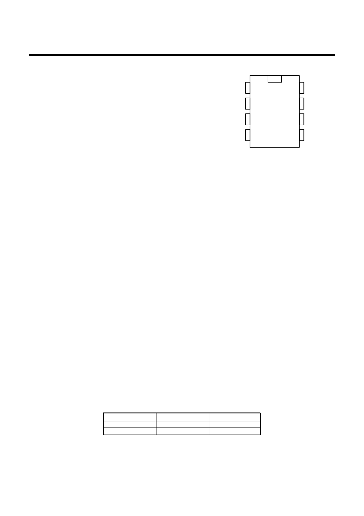
jfbkLQ QT301
P
RELIMINARY
Capacitance to Analog Converter (CAC) IC
Patented charge-transfer conversion method
Sub-ranging Direct-to-Analog conversion
Rescaleable PWM: wide dynamic range
End-to-end calibration (gain, span) via CAL pins
100 kHz PWM
Spread spectrum acquisition bursts for low noise
Sample on demand via Sync pin
Only one external sample capacitor
APPLICATIONS
C
APACITANCE TO
CAL_DN
A
NALOG
SYNC 1
SNS1
Transducer driver Moisture detection Fluid level sensors
Material sensors Position sensing Proximity sensors
C
ONVERTER
8
VDD
QT301
2
3
45
7
6
CAL_UP
PWM
SNS2VSS
The QT301 charge-transfer (QT) IC is a self-contained Capacitance-to-Analog-Converter (CAC) capable of detecting
femotofarad level changes in capacitance. This part is designed primarily for stand-alone instrumentation applications.
Primary applications include fluid level sensors, distance sensors, material detectors, transducer amplifiers for pressure and
humidity sensing functions, and other uses requiring quantified capacitance data.
Unlike other Quantum products, the QT301 does not process its acquired data. Its only output is raw, unprocessed data in
filterable PWM form that can be translated into an analog voltage by a simple RC network. This allows the designer to treat
the device as a CAC for measurement applications.
The PWM range is set via two inputs that control the starting and ending point of the conversion range. For example, if the
capacitance range of Cx is from 27pF to 38pF, the QT301 can be calibrated so that the PWM zero point occurs at 27pF, and
the endpoint (255) occurs at 38pF. In this way, the PWM range is optimized for the zone of interest. These calibration points
are stored in internal EEPROM and do not have to be reacquired after a power reset. This means that the resolution of the
part can be compared easily to other methods that might otherwise require 12 or more bits of overall resolution.
The device operates on demand via a sync input pin. The sync input can also be used to avoid external noise sources and
cross-interference from adjacent QRG capacitive sensors. Unique among capacitance sensors, this device features
spread-spectrum burst modulation, permitting extremely high noise rejection characteristics for very robust signals even in
high EMI environments.
The device requires only a single sampling capacitor (Cs) to acquire signals. The value of this capacitor controls the gain of
the sensor, and it can be adjusted over 2½ decades of range from 1nF to 500nF. No external switches, opamps, or other
components are required.
LQ
AVAILABLE OPTIONS
AVAILABLE OPTIONS
8-PIN DIPSOICT
A
A
Copyright © 2003 QRG Ltd QT301 R1.04 21/09/03
8-PIN DIPSOICT
QT301-D-00C to +700C
QT301-D-00C to +700C
-QT301-IS-400C to +850C
-QT301-IS-400C to +850C
Page 2
1 - Overview
3 to 5.5V
The QT301 is a digital burst mode charge-transfer (QT)
capacitance-to-analog converter (CAC). It has a PWM output
designed for applications such as fluid level sensing and
distance gauging; the PWM signal is eight bits in resolution.
The IC features two calibration inputs for end-to-end span
calibration. The output depends on load (Cx) and sampling
capacitor (Cs) values.
1.1 Basic Operation
The QT301 has internal EEPROM to store the two calibration
points. The sensor acquires the signal from the electrode and
calculates the PWM result using the two calibration points.
The sensor can be calibrated via the two calibration inputs
(see Section 4). The signal can be acquired either
continuously or it can be synchronized on an external signal.
The response time of the PWM depends largely on the
acquisition burst spacing.
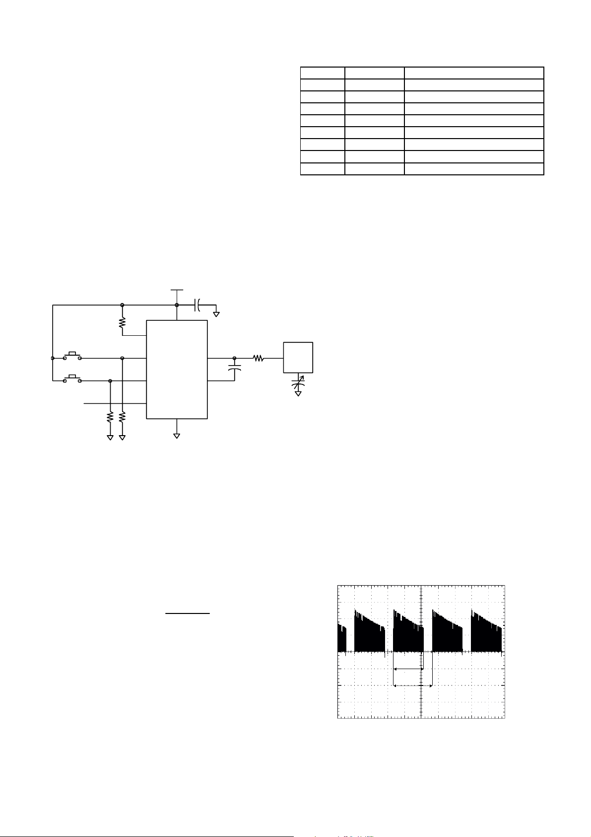
Figure 1-1 Basic Circuit Diagram
0.1uF
SYNC
CAL_UP
CAL_DN
PWM
166%10
VDD
VSS
8
4
Cx
SNS1
SNS2
3
5
3
Rs
Cs
R1
1
Uppe r Cal
7
Lowe r Cal
2
PWM Out
6
R2R3
1.2 Basic Circuit
Figure 1-1 shows a basic circuit diagram for the QT301. The
pin layout of the QT301 is as explained in Table 1-1. In this
particular circuit, C1 should be 100nF and R1, R2 and R3
should all be 10K.
R1 is only required if the synchronization feature is not used
and can be connected to either VDD or VSS.
Cs is recommended between 1nF and 500nF but this
depends on the sensitivity required. Use either NPO or PPS
capacitors for best results.
Rs is calculated with the following formula:
Rs <
where Cx is expressed in pF.
Table 1-1 Pin Description
FunctionNamePin
Sync InputSYNC1
Lower Calibration inputCAL_DN2
Sense 1 line (to electrode)SNS13
Negative supply (ground)VSS4
Sense 2 lineSNS25
PWM outputPWM6
Upper Calibration inputCAL_UP7
Positive supplyVDD8
2 - Signal Acquisition
The QT301 has a power-up delay of 200ms. During this
interval it does aquire signals or generate a PWM result; it
also ignores calibration inputs. This delay helps to prevent
false calibrations due to signal noise on Vdd during
startup.
Figure 2-1 shows the basic QT301 acquisition timing
parameters. Tbd is the burst duration, Tbs is the
burst spacing from the start of one burst to the start
of the next burst; when there is no Sync signal Tbs =
Tbd+2.5ms.
Electrode
provides direct ADC conversion. The ADC is designed to
dynamically optimize the QT burst length according to the
rate of charge buildup on Cs, which in turn depends on the
values of Cs, Cx, and VDD. VDD is used as the charge
reference voltage.
2.1 Burst Properties
The QT301 employs bursts of charge-transfer cycles
to acquire its signal. Burst mode dramatically reduces
RF emissions and lowers susceptibility to EMI.
The acquisition burst operates in a band between
Cx
230kHz and 305khz. The burst is spread-spectrum
modulated within this band to suppress interference
from external noise sources.
The QT switches and charge measurement hardware
functions are all internal to the QT301. A 16-bit
single-slope switched capacitor, analog to digital
converter (ADC), includes both the required QT
charge and transfer switches in a configuration that
Figure 2-1 Acquisition Burst: No Sync Pulse
LQ
Tbd
Tbs
2 QT301 R1.04 21/09/03
Page 3
2.2 CS / CX Dependency
The signal value is a direct function of Cs and Cx, where Cs
is the fixed sample capacitor, and Cx is the unknown
capacitance. These two values influence device sensitivity,
resolution and response time, making them very important
parameters.
Sensitivity and resolution are also a function of the size,
shape, and composition of the electrode, the composition
and thickness of any dielectric overlaying the electrode, the
composition and aspect of the object being sensed, and the
degree of mutual coupling between the electrode and the
object being sensed.
2.3 Burst Length
The burst length is described by the following formula:
BL =
Where ‘k’ is a constant, typical -0.51 (this may vary slightly
from device to device).
The response is thus a logarithmic curve; each doubling of
Cs increases the signal level and differential sensitivity by a
factor of two. Likewise, doubling Cx reduces the signal level
and differential sensitivity by a factor of two (Figures 6-1, 6-2,
page 8).
ln(
k
Cs
Cs+Cx
)
2.4 Sync Input
Bursts can be synchronized to external noise sources such
as mains frequency to suppress the effects of interference
coupled from such sources using a circuit such as that
shown in Figure 2-6. By synchronizing with noise sources,
the noise itself becomes highly correlated with the acquired
data, and AC alias components effectively disappear from
the signal. Sync works best on low frequency, highly
repeatable signals, such as mains frequency (50/60 Hz).
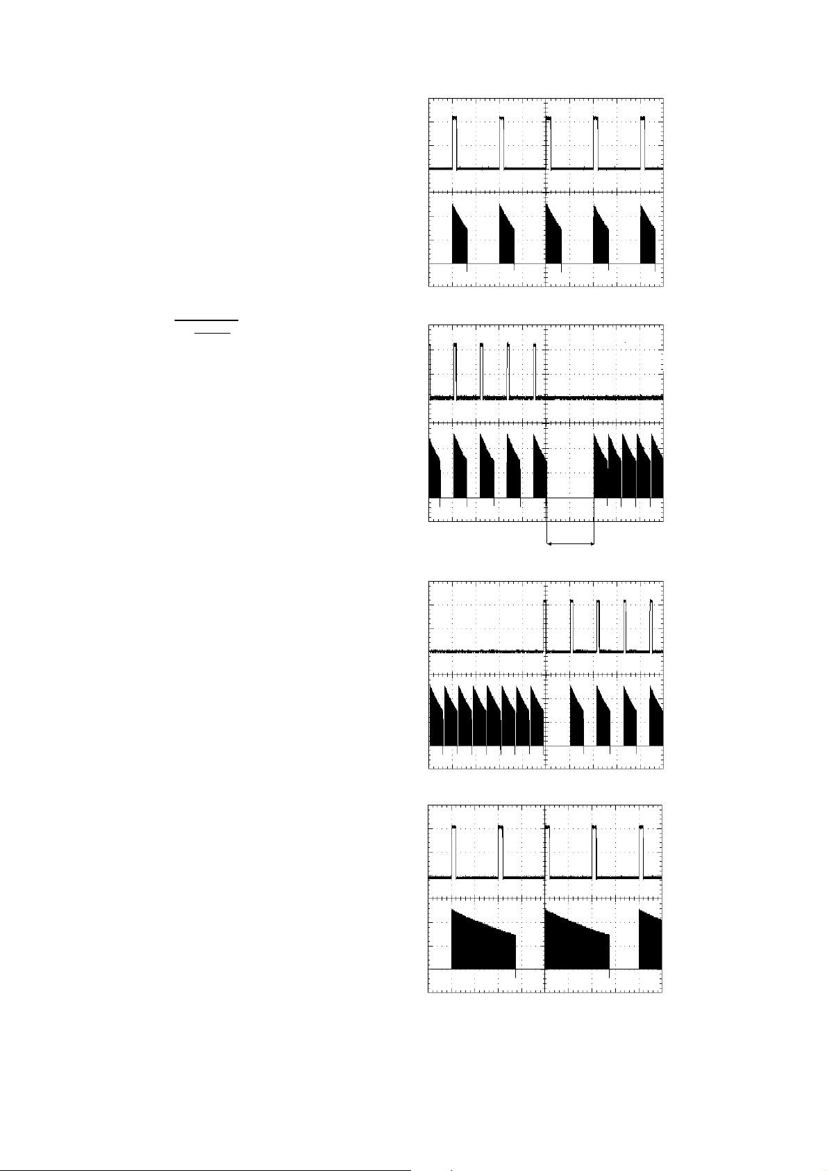
Figure 2-2 shows the effect of sync pulses on the burst rate.
A sync signal triggers a burst on the rising edge.
There is a Sync timeout of 100ms as shown in Figure 2-3. If
Sync pulses cease for >100ms, the Sync signal will be
treated as being lost and the device will start to acquire at its
own default rate again. When using the Sync feature it is
important that the Sync pulses are spaced less than 100ms
apart.
Figure 2-2 shows the acquisition burst in relation to Sync
pulses. If no rising edge is detected for 100ms, the QT301
will revert to the default timing shown in Figure 2-1. Figure
2-4 shows the sudden start of a train of Sync pulses and the
effect on the acquisition bursts.
Should the sync signal overclock the acquisition bursts
(Figure 2-5), the device will trigger on the next rising edge
after a delay of Tbd+2.5ms.
The 2.5ms is the minimum gap between bursts is to allow Cs
to properly discharge; Sync is not possible during this interval
nor is it possible to re-sync during a burst.
Figure 2-2 Acquisition Burst with Sync Signal
Sync Signal
Acquisition
Burst
Figure 2-3 Acquisition Burst: Sync Lost
Sync Signal
Acquisition
Burst
100ms
Figure 2-4 Acquisition Burst: Sync Reacquired
Sync Signal
Acquisition
Burst
Figure 2-5 Sync Overclocked
Sync Signal
Acquisition
Burst
LQ
3 QT301 R1.04 21/09/03
Page 4

Figure 2-6 Line Sync and PWM Output Filter
+3 to 5.5V
0.1uf
IN4148
Line
Frequency
Analog
Output
1M
20pF
Upper Cx Cal
Lower Cx Cal
100K
0.1uF
10K
3 PWM Output
The PWM output is a 100KHz ±7% square wave.
The PWM can be filtered using a simple RC circuit, or fed
directly into a timer circuit that can measure its duty cycle
with sufficient resolution. If an RC is used, the resistor should
be at least 10K ohms to reduce pin loading errors.
The PWM duty cycle is defined as follows:
T
D
PWM
If an RC circuit is used, it is often best to put a voltage
follower circuit on the output of the filter to buffer the output
voltage (Figure 2-6).
Note that the PWM output is not
capacitance from end to end. The transfer function for the
QT301 is a logarithmic response (Section 2.3).
During CAL, the PWM output value is locked in place with
the value just prior to when the CAL process was triggered.
Only after CAL is complete is the PWM updated with the new
results.
=
T
PWM_high
PWM_Period
linear with changes in Cx
8
SYNC
CAL_UP
CAL_DN
PWM
VDD
VSS
Electrode
3
SNS1
5
SNS2
4
Rs
Cs
Cx
1
7
2
6
10K
corresponding end point, without affecting the other end
point.
4.2 Calibration Process
The CAL pins are inputs used to trigger a CAL process on
the upper (max Cx) or lower (min Cx) capacitance endpoints.
These pins must be pulled low via a pulldown resistor on
each, to prevent damage.
To calibrate either endpoint, assert either CAL pin high using
an open-source output from a mosfet or microcontroller, or, a
collector from a PNP transistor whose emitter is connected to
Vdd. Hold this level high for 2.5ms minimum (preferably, 3ms
to be safe). Then release the pin to try to float down.
The QT301 will continue to hold the pin high starting at the
2.5ms point. There should be no contention problem with an
external voltage plus the QT301 both holding this pin high.
Figure 4-1 Calibration Process
User sets CAL_DN
high
User sets CAL_UP
high
4 Calibration
The QT301 should be calibrated end to end to have an
effective, properly scaled PWM output. The calibration is
done on a ‘learn by example’ basis. Each end is calibrated
separately while the appropriate end-point signal level is
applied. After the Cal process, the PWM signal will scale
itself to reflect these endpoints with the best resolution
possible.
4.1 Calibration Pins
The CAL_DN pin should be used to calibrate the signal when
the electrode is at its lowest level of Cx, for example with a
level probe when the fluid is at a minimum.
The CAL_UP pin should be used to calibrate the signal when
the electrode is at its maximum useable level of Cx, for
example with a level probe when the fluid is at the top.
It does not matter whether CAL_DN or CAL_UP are applied
first. After calibration is complete, either CAL_DN or CAL_UP
can be asserted again to obtain a fresh calibration for the
LQ
2.5ms Delay
CAL_DN forced high
by QT301
Calibration starts
User floats CAL_DN
NO
QT301 Cal done?
YES
QT301 floats
CAL_DN pin again
2.5ms Delay
CAL_UP forced high
by QT301
Calibration starts
User floats CAL_UP
NO
QT301 Cal done?
YES
QT301 floats
CAL_UP pin again
4 QT301 R1.04 21/09/03
Page 5

When the QT301 is done calibrating, it will release the CAL
pin in question to float low. A host controller can use this
feature to check when the calibration process has completed.
Calibration takes 15 acquisition burst samples to complete.
The new calibration data is stored in internal EEPROM when
the host releases the CAL pin to float low again; the chip also
begins to operate normally again at this time.
Figure 4-1 shows the control flows for calibration.
The capacitive signal on the electrode should be as stable
and noise-free as possible during the CAL intervals to ensure
accurate calibration points.
During a CAL cycle, the PWM output functions normally
using the last known good calibration data and signal value.
The PWM output will change again only when the CAL
process is complete.
Note: The CAL pins should never be driven low. Driving
either of the CAL pins low will short circuit the chip.
the ESD transients. In extreme cases, ESD dissipation can
be aided further by adding a resistor in series with the
electrode.
The charge pulse can be a minimum of 1µs and therefore the
circuit can tolerate values of series-R up to 18k in cases
where electrode Cx load is below 10pF. Extra diode
protection may be used at the electrodes but this often leads
to additional RFI problems as the diodes will rectify RF
signals into DC; this will disturb the sensing signals.
Series-R’s should be low enough to permit at least six RC
time-constants (i.e. a net RC timeconstant of 1/6 µs) to occur
during the charge pulse, where R is the added series-R and
C is the load Cx. If the series-R or Cx is too large, sensitivity
will be reduced.
Directly placing semiconductor transient protection devices
or MOV's on the sense leads is not advised; these devices
have extremely large amounts of non-linear parasitic C,
which will swamp the capacitance of the electrode and may
deliver spurious sensing results.
5 - CIRCUIT GUIDELINES
5.1 Sample Capacitor
The charge sampler capacitor (Cs) can be virtually any
plastic film or low to medium-K ceramic capacitor. The
acceptable Cs range is from 1nF to 500nF depending on the
sensitivity required; larger values of Cs demand higher
stability to ensure reliable sensing. Acceptable capacitor
types include plastic film (especially PPS film) and NP0/C0G
ceramic. X7R ceramic can also be used but this type is less
stable over temperature.
5.2 Power supply, PCB Layout
The QT301 makes use of the power supply as a reference
voltage. The acquired signal will shift slightly with changes in
VDD; fluctuations in VDD often happen when additional loads
are switched on or off such as LEDs etc.
Care should be taken when designing the power supply, as
any change in VDD will affect the PWM level.
If the power supply is shared with another electronic system,
make sure the supply is free of spikes, sags, and surges.
The supply is best locally regulated using a conventional
78L05 type regulator, or almost any 3-terminal LDO device
from 3V to 5V.
For proper operation, a 0.1µF or greater bypass capacitor
must be used between VDD and VSS; the bypass cap should
be placed very close to the device pins. The PCB should if
possible include a copper pour under and around the IC, but
not extensively under the SNS pins or lines.
5.3 ESD Protection
In cases where the electrode is placed behind a dielectric
panel the IC will be protected from direct static discharge.
However, even with a panel transients can still flow into the
electrodes via induction, or in extreme cases via dielectric
breakdown. Porous materials may allow a spark to tunnel
right through the material. Testing is required to reveal any
problems.
The device has diode protection on its SNS pins that absorb
most induced discharges (up to 20mA), and protect the
device. The usefulness of the internal clamping will depend
on the dielectric properties, panel thickness, and rise time of
5.4 RF Susceptibility
PCB layout, grounding, and the structure of the input circuitry
have a great bearing on the success of a design that can
withstand strong RF interference. The circuit is remarkably
immune to RFI provided that certain design rules are
adhered to:
1. Use SMT components to minimize lead lengths.
2. Connect electrodes to SNS1, not SNS2.
3. Use a ground plane under and around the circuit and
along the sense lines, that is as unbroken as possible
except for relief under and beside the sense lines to
reduce total Cx. Relieved rear ground planes along the
SNS lines should be ‘mended’ by bridging over them at
1cm intervals with 0.5mm ‘rungs’ like a ladder.
4. Ground planes and traces should be connected only to a
common point near the VSS pin of the IC.
5. Route sense traces away from other traces or wires that
are connected to other circuits.
6. Sense electrodes should be kept away from other
circuits and grounds which are not directly connected to
the sensor’s own circuit ground; other grounds will
appear to float at high frequencies and couple RF
currents into the sense lines.
7. Keep the Cs sampling capacitors and all series-R
components close to the IC.
8. Use a 0.1µF minimum, ceramic bypass cap very close to
the VSS/VDD supply pins.
9. Use series-R’s in the sense line of as large a value as
the circuit can tolerate without degrading sensitivity
appreciably (see Section 1.2).
10. Bypass input power to chassis ground and again at
circuit ground to reduce line-injected noise effects.
Ferrites over the power wiring may be required to
attenuate line injected noise.
Achieving RF immunity requires diligence and a good
working knowledge of grounding, shielding, and layout
techniques. Very few projects involving these devices will fail
EMC tests once properly constructed.
LQ
5 QT301 R1.04 21/09/03
Page 6

6 Electrical specifications
V
V
V
V
V
V
V
@
V
6.1 ABSOLUTE MAXIMUM SPECIFICATIONS
Operating temp................................................................................ as designated by suffix
Storage temp....................................................................................... -65
Vdd......................................................................................................-0.5 to +6V
Max continuous pin current, any control or drive pin..............................................................±40mA
Short circuit duration to ground, any pin......................................................................... infinite
Short circuit duration to VDD, any pin........................................................................... infinite
Voltage forced onto any pin....................................................................-1V to (VDD + 0.5) Volts
6.2 RECOMMENDED OPERATING CONDITIONS
Vdd........................................................................................................ +3 to 5V
Short-term supply ripple+noise..................................................................................±5mV
Long-term supply stability.................................................................................... ±100mV
Cs value................................................................................................. 1 to 500nF
Cx value..................................................................................................0 to 500pF
6.3 GENERAL SPECIFICATIONS
WC
PU
100,000EEPROM write cyclesE
ms200Power up timeT
pF11Sensor pin internal capacitance Csns
-0.51Burst length coefficientK
6.4 AC SPECIFICATIONS
VDD = 3.3 Volts, Cs = 100nF, Cx = 5pF, Ta = recommended range, unless otherwise noted
PC
D
BD
BS
PWM
CPD
CD
Calibration durationT
BS
µs1.51.251Charge/transfer timeT
kHz265Burst center frequencyFc
%±7Burst frequency modulationF
ms16Burst lengthT
msTBD + 100TBD + 2.5Burst spacingT
kHz100PWM frequencyF
ms2.5Calibration pulse durationT
ms15 x T
+/-10% over voltage and
temperature range
O
C to +125OC
NotesUnitsMaxTypMinDescriptionParameter
NotesUnitsMaxTypMinDescriptionParameter
6.5 DC SPECIFICATIONS
VDD = 3.3 Volts, Cs = 100nF, Cx = 5pF, Ta = recommended range, unless otherwise noted
DD
DD
IL
IH
OL
OH
R
LQ
0.6 VDDInput high voltage
DD-0.7High output voltage
6 QT301 R1.04 21/09/03
mA2.9Supply currentI
bits11Acquisition resolutionA
fF8Resolution per bitS
NotesUnitsMaxTypMinDescriptionParameter
@5VmA5Supply currentI
3.3
VDD = 3 to 5.5VV0.3 VDDInput low voltageV
DD = 3 to 5.5
IOL = 6mAV0.5Low output voltageV
IOH = -1.5mA
Page 7

10000
s
A
9000
8000
7000
6000
200nF
120nF
80nF
40nF
1000
900
800
700
600
22nF
10nF
4.7nF
5000
4000
Burst Length ,counts
3000
2000
1000
0
0 1020304050
Cx Load
Figure 6-1 Typical Burst Length versus Cx & Cs;
VDD = 5.0 Volts
5.0
4.5
4.0
3.5
500
400
Burst Length ,count
300
200
100
0
0 1020304050
Cx Load
Figure 6-2 Typical Burst Length versus Cx & Cs;
VDD= 5.0 Volts
3.0
Current Consumption, m
2.5
2.0
2.5 3.0 3.5 4.0 4.5 5.0 5.5
Power supply, Volts
Figure 6-3 Power Consumption versus VDD
LQ
7 QT301 R1.04 21/09/03
Page 8

Figure 6-4 Typical Signal Deviation versus Temperature
VDD = 5.0 Volts, Cx = 10pF
6000
5000
4000
3000
Signal, Counts
2000
1000
0
-10 0 10 20 3 0 40 50 60 70 80
Temperature, °C
200nF PP S
100nF PP S
4.7nF PP S
Figure 6-5 Typical Signal Deviation vs. Temperature
Vdd = 5.0 Volts, Cx = 10pF, Cs = 5nF - 200nF PPS Film
5.00%
4.00%
3.00%
2.00%
1.00%
0.00%
-1.00%
% Deviation
-2.00%
-3.00%
-4.00%
-5.00%
-10-5 0 5 10152025 30354045 5055606570 758085
Temperature, C
LQ
8 QT301 R1.04 21/09/03
Page 9

x
yp
A
Pin 1
M
M
Symbol
F
A
S1
a
A
r
S
L2
x
m
Q
L1 L
Package type: 8-pin Dual-In-Line
InchesMillimeters
NotesMaxMinNotesMaxMin
0.280.247.116.1a
0.3250.38.267.62
0.40.35510.169.02M
0.0370.0270.940.69Q
0.0220.0140.5590.356L
0.070.0451.781.14L1
0.0120.0080.3050.203L2
-0.015-0.38r
0.150.1153.812.92S
0.21-5.33-S1
0.4310.9
T
ical-0.3Typical-7.62m
BSC-0.1BSC-2.54F
Symbol
φ
Pin 1
a
FL
Package type: 8-pin Wide SOIC
o
0
o
8
M
A
H
φ
h
e
E
InchesMillimeters
NotesMaxMinNotesMaxMin
0.2130.2055.415.21a
0.330.38.387.62A
0.2120.2035.385.16M
0.020.0120.5080.305L
0.0130.0040.330.102h
0.080.072.031.78H
0.010.0070.2540.178e
0.0350.020.8890.508E
o
0
o
8
BSC0.05BSC1.27F
LQ
9 QT301 R1.04 21/09/03
Page 10

lQ
Copyright © 2003 QRG Ltd. All rights reserved.
Patented and patents pending
Corporate Headquarters
1 Mitchell Point
Ensign Way, Hamble SO31 4RF
Great Britain
Tel: +44 (0)23 8056 5600 Fax: +44 (0)23 8045 3939
admin@qprox.com
www.qprox.com
North America
651 Holiday Drive Bldg. 5 / 300
Pittsburgh, PA 15220 USA
Tel: 412-391-7367 Fax: 412-291-1015
The specifications set out in this document are subject to change without notice. All products sold and services supplied by QRG are subject
to our Terms and Conditions of sale and supply of services which are available online at www.qprox.com and are supplied with every order
acknowledgement. QProx, QTouch, QMatrix, QLevel, and QSlide are trademarks of QRG. QRG products are not suitable for medical
(including life-saving equipment), safety or mission critical applications or other similar purposes. Except as expressly set out in QRG's
Terms and Conditions, no licenses to patents or other intellectual property of QRG (express or implied) are granted by QRG in connection
with the sale of QRG products or provision of QRG services. QRG will not be liable for customer product design and customers are entirely
responsible for their products and applications which incorporate QRG's products.
 Loading...