

LQ QT300
C
APACITANCE TO
Capacitance to Digital Converter (CDC) IC
Direct-to-digital conversion, 16 bits
Log response: Wide dynamic range
Outputs raw data to a host device
Single wire UART interface
Master or Slave mode SPI interface
Programmable clock speed
Turns objects into intrinsic touch sensors
One external sample capacitor to control gain
Multiple QT300’s possible on one SPI bus
The QT300 charge-transfer (“QT’”) IC is a self-contained Capacitance-toDigital-Converter (CDC) capable of detecting femotofarad level changes in
capacitance. While designed primarily for instrumentation applications, it can be used
also for touch control applications where signal processing is best handled by a host
MCU.
Primary applications include fluid level sensors, distance sensors, transducer
‘amplifiers’ for pressure and humidity sensing functions, material detectors, and other
uses requiring quantified capacitance data.
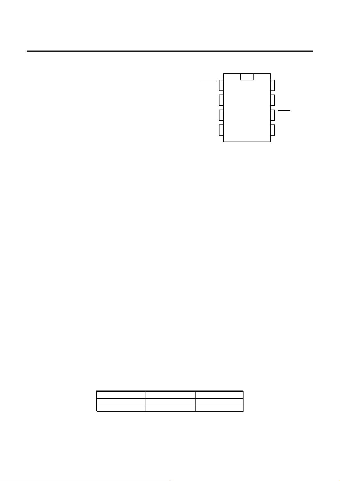
DRDY 1
SCK
SNS1
D
IGITAL
C
ONVERTER
8
Vdd
QT300
7
6
SDO
REQ / 1W
SNS2Vss
2
3
45
APPLICATIONS
Fluid level sensors
Prox sensors
Moisture detection
Position sensing
Transducer driver
Material sensors
Unlike other Quantum products, the QT300 does not process its acquired data. Its only result is raw, unprocessed binary
data which can be transmitted to a host via either a bidirectional SPI interface or a simple polled single wire UART type
interface. This allows the designer to treat the device as a capacitance-to-digital-converter (CDC) for measurement
applications. It is ideal for situations where there are unique signal processing requirements.
The device requires only a single sampling capacitor to function. The value of this capacitor controls the gain of the sensor,
and it can be adjusted over 2½ decades of range from 1nF to 500nF. No external switches, opamps, or other components
are required.
The device operates on demand, and can be synchronized to allow several QT300’s to operate near each other without
cross-interference.
AVAILABLE OPTIONS
A
0
C to +700C
8-PIN DIPSOICT
QT300-D-0
-QT300-IS-400C to +850C
LQ
Copyright © 2002 QRG Ltd QT300 R1.01 21/09/03
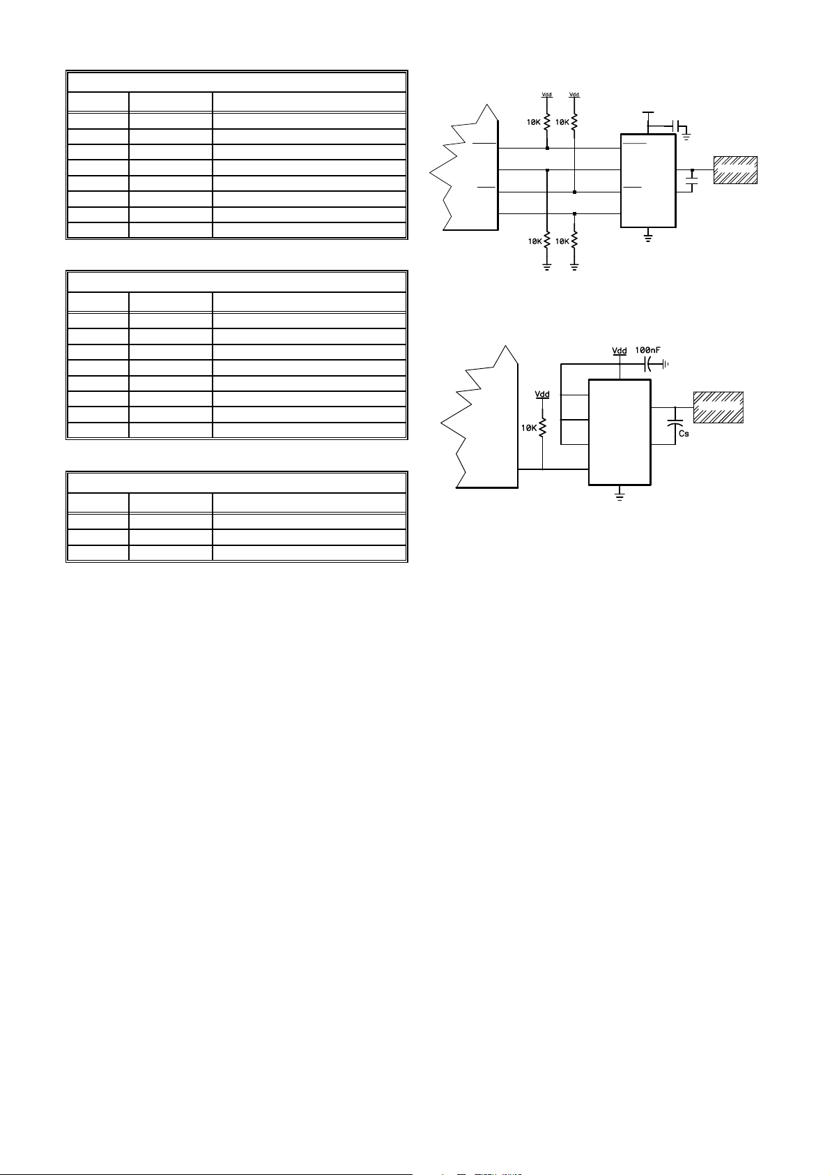
Table 1-1 SPI Mode Pin Description
FunctionNamePin
Data Ready/DRDY1
Serial data clockSCK2
Sense 1 lineSNS13
Negative supply (ground)VSS4
Sense 2 lineSNS25
Request input/REQ6
Serial data outSDO7
Positive supplyVDD8
Table 1-2 1W UART Mode Pin Description
FunctionNamePin
Connect to Vdd or Vss-1
Connect to Vdd or Vss-2
Sense 1 lineSNS13
Negative supply (ground)VSS4
Sense 2 lineSNS25
1W UART Line1W6
Connect to Vdd or Vss-7
Positive supplyVDD8
Table 1-3 Alternate Cloning Pin Functions
FunctionNamePin
Serial clone data clockSCK2
Serial clone data inSDI6
Serial clone data outSDO7
1 - OVERVIEW
The QT300 is a digital burst mode charge-transfer (QT)
capacitance-to-digital converter (CDC) designed for
applications requiring raw signal information such as fluid
level sensing and distance gauging; it outputs raw digital
signal data over a serial interface. The output data is in a
16-bit format; signal levels depend on load (Cx) and the
sampling capacitor value (Cs).
1.1 Basic Operation
The QT300 does no internal signal processing; data is simply
returned via one of two serial port types.
There are two basic types of serial interface: 4-wire SPI and
a simple single wire (‘1W’) UART. The SPI interface allows
multiple devices to be connected on one SPI bus, while
the1W UART requires that the controller have one dedicated
pin for each QT300. There are two types of SPI mode,
master and slave.
The type of serial port and its mode can be selected via the
cloning process using a QTM300CA programming adapter.
The QT300 operates only on request from a host device.
After initiation via a trigger signal, the QT300 generates an
acquisition burst and sends the resulting raw signal data
back via one of the serial modes.
Vdd
SCK
SDO
8
Vcc
GND
4
SNS 1
SNS 2
100nF
3
SENSOR
5
CS
DRDY
SCK
Host Micro
REQ REQ
SDI
QT 300
1
2
6
7
DRDY
Figure 1-1 Basic QT300 Circuit in SPI mode.
QT300
8
Vdd
Host Micro
(1W UART)
1
2
7
Rx
6
1W
Vss
4
SNS1
SNS2
3
5
Electrode
Figure 1-2 Basic QT300 Circuit in UART mode.
1.2 CS / CX Dependency
The value returned is a direct function of Cs, the fixed sample
capacitor and Cx, the unknown or variable capacitance.
These two values influence device sensitivity and response
time, making them very important parameters.
Sensitivity is also a function of electrode size, shape,
orientation, the composition and aspect of the object being
sensed, the thickness and composition of any dielectric
overlaying the electrode, and the degree of mutual coupling
between the electrode and the object being sensed.
The response follows a logarithmic curve (Figures 7-4, 7-5,
Page 10); each doubling of Cs increases the signal level and
differential sensitivity by a factor of 2. Likewise, doubling Cx
reduces the signal level and differential sensitivity by a factor
of 2.
2 - Timing
Figure 2-1 shows the basic QT300 acquisition timing
parameters. The basic timing parameters are:
Tbd Burst duration (2.1)
Tacq Acquire response time (2.2)
Tbs Burst Spacing (2.3)
2.1 Tbd - Burst duration
The burst duration depends on the values of Cs and Cx and
to a lesser extent, Vdd. The burst is composed of
charge-transfer cycles operating at about 240kHz.
LQ
2
QT300 R1.01 21/09/03
The length of this burst is an important
parameter as it is directly related to the signal
value. The burst duration also affects the
response time of the sensor; the larger Cs is, the
longer the burst, the slower the possible
acquisition rate.
2.2 Tacq - Acquire Response Time
The time from the /REQ or 1W line going low
until the completion of data transmission is
Tacq. Tacq depends on the acquisition burst
length as well as the serial transmission time.
SPI Mode: In SPI mode Tacq depends in part on
the serial clock speed and the space between
the returned high and low bytes. In SPI slave
mode the clock speed and the inter-byte spacing
time Tbdly is determine by the host. In SPI
Master mode these timings are set by Setup
parameters SCD and MLS.
1W mode: Tacq depends in part on the Baud
rate as well as the inter-byte spacing. The Baud
rate is auto-set by the trigger pulse width; the
inter-byte spacing is set by the MLS parameter.
See Section 4.
2.3 Tbs - Burst Spacing
Burst spacing is the time from the start of one
acquisition burst to the start of the next burst. It
depends on the host’s trigger rate on the /REQ or 1W pin.
The QT300 only acquires when the host requests it.
While waiting for a new request the part is in a low power
mode.
3 - SPI Port
3.1 SPI Specifications
The QT300 can operate in master or slave mode, and thus is
compatible with virtually all SPI-capable microcontrollers. The
SPI interface has the following specifications:
Max clock rate, Fckm 40KHz (master mode)
Max clock rate, Fcks 40KHz (slave mode)
Data length 2 bytes (16 bits total)
Inter-byte delay ≥8µs (master mode)*
≥12µs (slave mode)
Clock idle logic level Low or High*
Clock edge Data out on rising or falling edge*
Data sequence High byte first, MSB first
*Determined by Setups
The host can clock the SPI at any rate up to and including
the maximum. The maximum clock rate of the part in Master
mode is determined in Setups via cloning.
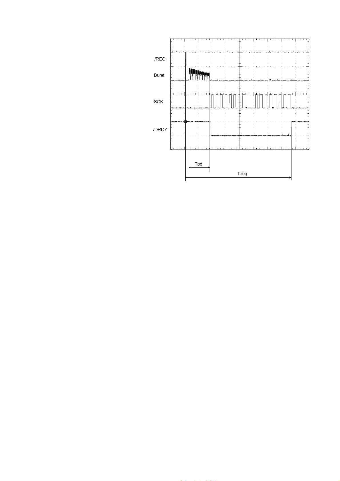
3.2 Protocol Overview
The QT300 only transmits data on request, after an
acquisition burst. The host requests an acquire by setting the
/REQ line low for at least 30µs; the device then acquires.
When finished, the DRDY line is pulled low by the QT300 to
indicate it is ready to send data. (Figure 2-1). The transfer is
done as two bytes, with the highest byte transferred first.
Figure 2-1 Signal Acquisition - Slave SPI Mode
In master mode, /DRDY goes high between bytes for the
period determined by Setup parameter MLS; this is a multiple
of 6µs.
When not communicating, all SPI lines float to allow multiple
chips to connect over the same SPI lines. A pullup or
pulldown resistor is required on SCK depending on the
selected clock phase, determined by Setups. A pullup
resistor is required on /DRDY. /REQ may require a pullup if
the host ever allows this line to float.
3.3 SPI Bus Sharing
All SPI float transfers making it possible to have several
QT300 devices (or other unrelated devices) share the SPI
control signals (Figure 3-1).
Each part needs an individual /REQ line, but /DRDY, SCK
and SDO can be connected together.
3.4 SPI Slave Mode
Refer to Figure 7-1 and Table 7-1, page 8.
In SPI Slave mode, /DRDY is used to let the host know when
data is ready for collection in response to a request so that
the host can clock over the data.
SPI Slave mode uses 4 signals:
/REQ - Request Acquisition Input; Active low input-only.
When /REQ is pulled low, the QT300 wakes and starts an
acquire. The IC will transmit the resulting data only when
the acquire has finished.
/REQ should return high before the end of the burst. If
/REQ is still low at the end of the burst the part will go into
Setup mode. The minimum duration of /REQ is 30µs.
LQ
3
QT300 R1.01 21/09/03
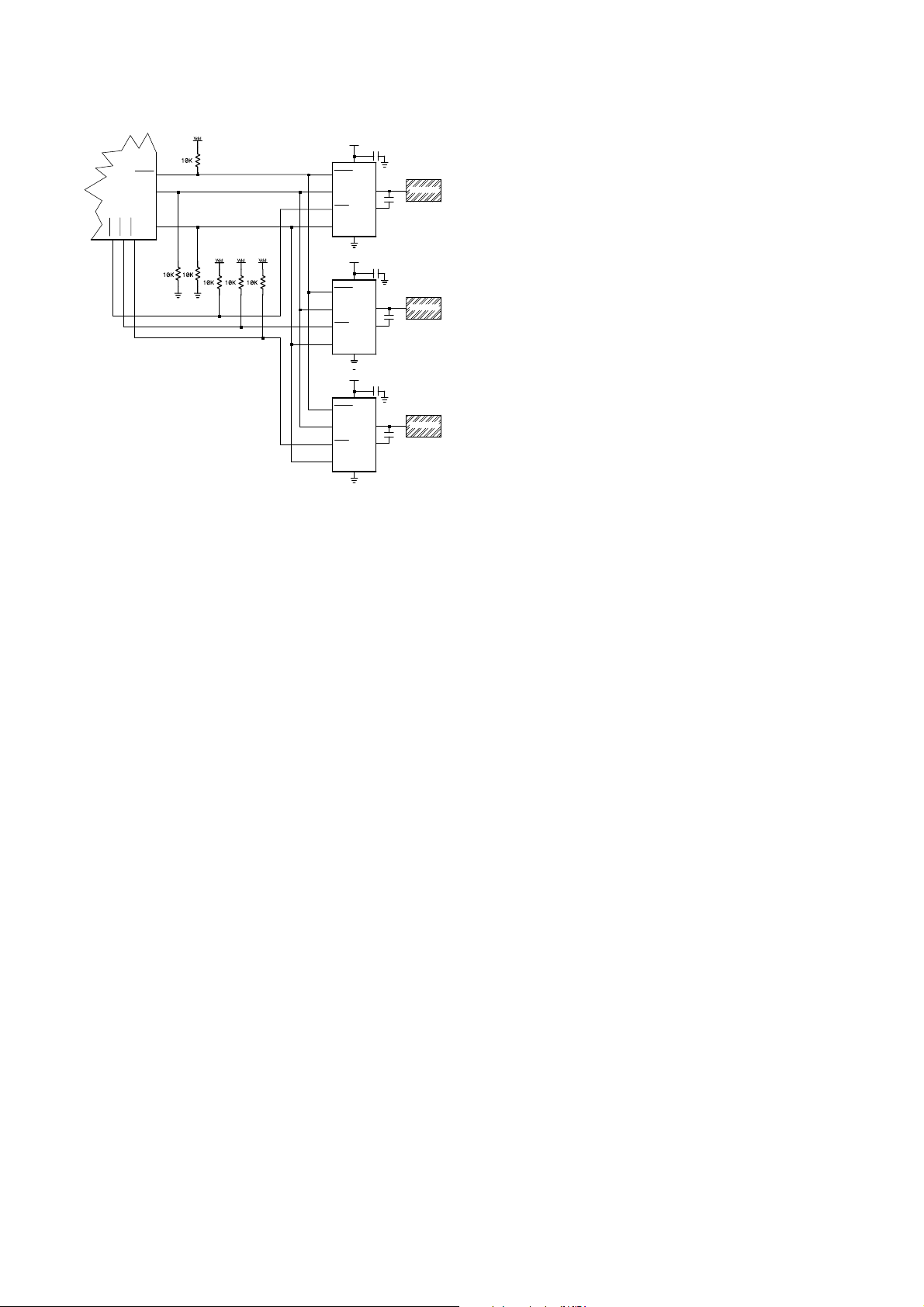
Figure 3-1 Multiple QT300's on the same SPI port
Vdd
100nF
8
QT 300
Vcc
1
QT 300
QT 300
DRDY
SCK
REQ
SDO
DRDY
SCK
REQ
SDO
DRDY
SCK
REQ
SDO
3
100nF
100nF
SENSOR
5
CS
3
SENSOR
5
CS
3
SENSOR
5
CS
SNS 1
SNS 2
GND
4
Vdd
8
Vcc
SNS 1
SNS 2
GND
4
Vdd
8
Vcc
SNS 1
SNS 2
GND
4
2
6
7
1
2
6
7
1
2
6
7
Host Micro
REQ1
REQ2
DRDY
REQ3
SCK
SDI
SDO - Serial Data Output; Output-only. This is the data
output to the host during an SPI transfer. When not in use,
this pin floats. This pin should be connected to the SDI
input pin of the host device.
SCK - SPI clock; Idle high or idle low; input-only SPI clock
from the host. The idle state is determined in Setups by
the serial mode (SM) parameter.
If SM is set for idle-low SCK: Data is shifted out of the
QT300 on the rising edge of SCK and should be shifted
into the host on the falling edge of SCK.
If SM is set for idle-high SCK: Data is shifted out of the
QT300 on the falling edge of SCK and should be shifted
into the host on the rising edge of SCK.
The maximum clock speed is 40kHz, and the timings
should obey the parameters Tskh and Tskl in Table 7-1.
/DRDY - Data Ready; active low output only. This indicates to
the host that the device is ready to send data back to the
host. During idle times this pin floats and therefore must
be connected to a pullup resistor. The host must wait until
/DRDY goes low before starting an SPI transfer.
Between the high and low byte clockings, the host should
observe a delay of ≥12µs.
A typical SPI slave mode communication sequence is:
1) Host pulses /REQ low for ≥30µs to initiate an acquire.
2) QT300 acquires a signal in response to /REQ.
3) QT300 pulls /DRDY low when ready to send data back.
4) Host detects /DRDY is low.
5) Host clocks out the high byte of data from the QT300.
6) Host waits for ≥12µs.
7) Host clocks out the low byte of data from the QT300.
8) QT300 releases /DRDY to float high.
3.5 SPI Master Mode
Refer to Figure 7-2 and Table 7-2, page 8.
In master SPI mode the QT300 generates the clock signal
after an acquire initiated from the host via the /REQ line. The
clock speed and the spacing between the two bytes is set via
the Setup process (Section 6).
SCD setup parameter determines the master-mode clock
rate. The default value is 55 (resulting in a 2.55KHz rate).
The relationship is:
Fscd = 1200/(30+ (SCD x 8)) in Khz
Where SCD = 0..255
MLS setup parameter determines the spacing between the
two return bytes; this can be important to allow a slow host
device to recover from receiving the first byte to prevent an
overrun. The default value is 148 (resulting in a 500µs gap).
The relationship is:
Tmls (in µs) = (10 + MLS x 4) / 1.2
Where MLS = 0..255 (from user setup MLS)
Master SPI mode requires at least 3 signals to operate:
/REQ - Request Acquisition Input; Active low input-only.
When /REQ is pulled low, the QT300 wakes and starts an
acquire. The IC will transmit the resulting data only when
the acquire has finished.
/REQ must return high before the end of the burst. If
/REQ is still low at the end of the burst the part goes into
Setup mode. The minimum duration of /REQ is 30µs.
SDO - Serial Data Output; Idle low output-only. This is the
data output to the host during an SPI transfer. When not in
use, this pin floats. This pin should be connected to the
SDI input pin of the host device.
SCK - SPI clock; Idle high or idle low, output-only. The idle
state is determined in Setups by the serial mode (SM)
parameter.
If SM is set for idle-low SCK: Data is shifted out of the
QT300 on the rising edge of SCK and should be shifted
into the host on the falling edge of SCK.
LQ
If SM is set for idle-high SCK: Data is shifted out of the
QT300 on the falling edge of SCK and should be shifted
into the host on the rising edge of SCK.
The maximum clock speed is 40kHz, and the timings
should obey the parameters Tskh and Tskl in Table 7-2.
/DRDY - Data Ready (Optional); active low output only. This
indicates to the host that the device is ready to send data
4
QT300 R1.01 21/09/03
4 Single-Wire (1W) UART
Interface
The single wire ('1W') UART option allows all
communications to take place over a single
bidirectional line with a 10K pullup resistor. The host
device triggers the QT300 to acquire by means of a
pulse sent to the QT300 over the wire. The Baud rate
is established by the width of this pulse; the pulse
width establishes the bit rate of the UART
transmission to follow. The QT300 then acquires, and
responds by sending two bytes of data back over the
1W line with a delay between the bytes as determined
by parameter MLS.
1W operation permits a device to be controlled from a
single pin on a host controller, using either a hardware
or software UART. Several QT300’s can coexist on a
single host pin, provided there is some logic steering.
This mode is set via the cloning process using
parameter SM (see Section 6).
4.1 1W UART Specifications
The QT300 operates in 1W UART mode with the
following specifications:
Baud rate range 4,800 to 9,600 bits/sec
Data length 2 bytes (16 bits total)
Stop bit 1 (each byte)
Parity None
Idle state High
The 1W line must have a pullup resistor on it (i.e.
10K), or 1W communications will not function.
Figure 4-1 UART and Trigger Pulse Signal.
back to the host. During idle times this pin floats and
therefore must be connected to a pullup resistor.
The DRDY line can be used as a Slave Select line (SS).
The host does not need this line to operate in many cases.
DRDY can be used to 'frame' byte transmissions.
Between bytes /DRDY will go high for a period determined
by the MLS setup parameter; the minimum period is 8.3µs.
A typical Master mode SPI sequence is:
1) Host pulses /REQ low for ≥30µs.
2) QT300 acquires a signal in response to /REQ.
3) QT300 pulls /DRDY low when ready to send data.
4) Host detects /DRDY low and prepares to receive data.
5) QT300 clocks out first byte of data (MSB).
6) QT300 sets /DRDY high for a duration determined by
Setup parameter MLS.
7) QT300 pulls /DRDY low.
8) QT300 clocks out the low byte (LSB).
9) QT300 releases /DRDY to float high.
4.2 UART 1W Protocol
The QT300 acquires and transmits only on request.
The sequence is:
1) The host generates a pulse on the 1W pin; the
pulse width must match the Baud rate (bit width)
of the expected return Baud rate from the QT300.
This pulse actually sets the Baud rate each time,
and so it can vary from one acquire to another. See
Section 4.3 and Figure 4-1.
2) The 1W pulse width is measured by the QT300 to
determine the Baud rate.
3) The host floats 1W high.
4) The QT300 acquires the signal to completion.
5) QT300 returns data in the following UART format:
start bit (low)
8 bits, high byte
stop bit (high)
delay (determined by MLS setup)
start bit (low)
8 bits, low byte
stop bit (high)
6) The QT300 floats the 1W line and enters idle mode.
LQ
5
QT300 R1.01 21/09/03

4.3 Trigger pulse description
The part wakes from low power mode when the first negative
edge is detected on the 1W pin (Figure 4-1, bottom). The
negative pulse must be at least 30µs wide.
The host then generates the positive pulse that actually sets
the Baud rate. The QT300 measure this pulse and uses its
length to set the Baud bit (shift out) rate. 30µs (or more) of
logic-low must follow this pulse.
The host must then float the 1W line to allow the QT300 to
start the signal acquisition.
5.3 PCB LAYOUT
5.3.1 G
The use of ground planes around the device is encouraged
for noise reasons, but ground or power should not be
coupled too close to the sense pins in order to reduce Cx
load. Likewise, the traces leading from the sense pins to the
electrode should not be placed directly over a ground plane;
rather, the ground plane should be relieved by at least 3
times the width of the sense traces directly under it, with
periodic thin bridges over the gap to provide ground
continuity.
ROUND PLANES
5 Circuit Guidelines
5.1 Sample capacitors
Cs capacitors can be virtually any plastic film or low to
medium-K ceramic capacitor. The normal usable Cs range is
from 1nF ~ 500nF depending on the sensitivity required;
larger values of Cs require higher stability to ensure low drift.
Acceptable capacitor types include NP0 or C0G ceramic,
PPS film, and Y5E and X7R ceramics in that order.
5.2 Power Supply
5.2.1 S
The QT300 makes use of the power supply as a reference
voltage. The acquired signal will shift slightly with changes in
Vdd; Vdd fluctuations often happen when additional loads
are switched on or off such as LEDs etc.
If the power supply is shared with another electronic system,
care should be taken to assure that the supply is free of
spikes, sags, and surges. It is best practice to use a
regulator just for the QT300 (or one for a set of QT300's).
5.2.2 S
Vdd can range from 2 to 5 volts nominal. Current drain will
vary depending on Vdd. During writing of the internal
EEPROM, Vdd must be at least 2.2 volts.
If desired, the supply can be regulated using a conventional
regulator, for example CMOS LDO regulators, or standard
78Lxx-series 3-terminal devices.
For proper operation a 100nF (0.1uF) ceramic bypass
capacitor must
cap should be placed very close to the Vdd and Vss pins.
TABILITY
UPPLY REQUIREMENTS
be used between Vdd and Vss; the bypass
5.3.2 N
OISE SYNCHRONIZATION
External fields can cause interference leading to a noisy and
unstable signal. The most common external fields usually are
from AC mains power.
The /REQ line of the QT300 can be used to synchronize the
acquisition to a repetitive external source of interference
such as the power line frequency in order to dramatically
reduce signal noise.
If line frequency is present near the sensors, this feature
should be used.
6 Parameter Setups Cloning
A special interface is provided to allow user-defined Setups
to be loaded into internal eeprom or read back out for
development and production purposes.
The QTM300CA cloning board in conjunction with QT3View
software simplifies the Setups cloning process greatly. The
E3A eval board has been designed with a connector to
facilitate direct connection with the QTM300CA. The
QTM300CA in turn connects to any PC with a serial port
which can run QT3View software (included with the
QTM300CA and available free on Quantum’s web site).
The connections required for cloning are shown in Figure
6-1. Further information on the cloning process can be found
in the QTM300CA instruction guide. The parameters which
can be altered are shown in Table 7-4.
The internal eeprom has a life expectancy of 100,000
erase/write cycles and the minimum voltage for a write cycle
is 2.2 Volts.
A serial interface specification for the device can be obtained
by contacting Quantum.
LQ
Cloning Signal
Vdd
SCK
REQ
SDO
8
Vcc
GND
4
100nF
SNS 1SCK
SNS 2
3
5
SENSOR
CS
DRDY
REQ
SDI
SDO
SDI
SCK
GND
QT 300
1
DRDY
2
6
7
Figure 6-1 Clone interface wiring
6
QT300 R1.01 21/09/03
7 Electrical specifications
V
V
V
V
7.1 ABSOLUTE MAXIMUM SPECIFICATIONS
Operating temp................................................................................ as designated by suffix
Storage temp....................................................................................... -65
V
DD
...................................................................................................... -0.5 to +6V
Max continuous pin current, any control or drive pin..............................................................±40mA
Short circuit duration to ground, any pin......................................................................... infinite
Short circuit duration to V
DD
, any pin............................................................................ infinite
Voltage forced onto any pin.................................................................... -1V to (Vdd + 0.5) Volts
7.2 RECOMMENDED OPERATING CONDITIONS
VDD........................................................................................................ +2 to 5V
V
DD
min required to reprogram eeprom Setups................................................................... +2.2V
Short-term supply ripple+noise..................................................................................±5mV
Long-term supply stability.................................................................................... ±100mV
Cs value................................................................................................. 1 to 500nF
Cx value..................................................................................................0 to 100pF
7.3 AC SPECIFICATIONS
Vdd = 3.0, Ta = recommended operating range, Cs=100nF unless noted
NotesUnitsMaxTypMinDescriptionParameter
PC
BL
RQP
ns830Charge/transfer durationT
Cs = 4.7nF to 200nF; Cx = 0ms250.5Burst lengthT
µs30Request pulseT
O
C to +125OC
7.4 DC specifications
Vdd = 3.0V, Cs = 10nF, Cx = 5pF, Ta = recommended range, unless otherwise noted
V5.52Supply voltageV
V0.4Low output voltageV
VVdd-0.6High output voltageV
bits16Acquisition resolutionA
DD
DD
OL
OH
IL
IH
R
0.6 VddInput high voltage
NotesUnitsMaxTypMinDescriptionParameter
Dependent on duty cycleµA1,50060Supply currentI
Vdd = 2.5 to 5.0VV0.3 VddInput low voltageV
dd = 2.5 to 5.0
Figs 7-4, 7-5fF71,000Resolution per bitS
LQ
7
QT300 R1.01 21/09/03
{from QT300}
T
DRDY
SCK
{from host}
SDO
{from QT300}
DRDY
{from QT300}
Tskd
D15
D14 D13 D12 D11 D10 D9 D8 D7 D6 D5 D4 D3 D2 D1 D0
Tds
Ts kh
Ts kl
Tmls
Ts o s h
Figure 7-1 SPI Slave Mode
mls
Tskd
Tsk h
Ts kl
Thso
T
SKD
SKH
SKL
SOSH
HSO
MLS
T
DS
{from QT300}
SCK
SDO
{from QT300}
SCK High To SDO Ready
Setup Time
DRDY Low To SCK High
Delay
Table 7-1 Slave SPI Timing
D15
D14 D13 D12 D11 D10 D9 D8 D7 D6 D5 D4 D3 D2 D1 D0
Tds
Ts osh
Figure 7-2 SPI Master Mode
UnitsmaxminParameterSymbol
-25Clock DurationT
-13SCK High DurationT
-12SCK Low DurationT
10-
-7SDO Hold TimeT
1,00012MSB-LSB SpacingT
1,00012
µs
µs
µs
µs
µs
µs
µs
SKD
SKH
SKL
SCK High To SDO Ready
T
SOSH
HSO
MLS
T
DS
Setup Time
DRDY Low To SCK High
Delay
Table 7-2 Master SPI Timing
Thso
1,72525Clock DurationT
862.512.5SCK High DurationT
862.512.5SCK Low DurationT
1,7088.3MSB-LSB SpacingT
UnitsmaxminParameterSymbol
µs
µs
µs
74
µs
--12.5SDO Hold TimeT
µs
--12.5
LQ
8
QT300 R1.01 21/09/03

1W UART
Twu
Tbr
Ts b
Tacq
Ts t a r t
Figure 7-3 1W UART Mode
8 x Tbr-MSB
8 x Tbr-LSB
Table 7-3 1W UART Timing
8bits MSB 8bits LSB
Tmls
Tstop
-5,00030Wake levelTwu
-210104Baud set pulseTbr
-5,00030Baud end levelTsb
-9,6004,800Baud rate range
-TbrStart pulseTstart
-TbrStop pulseTstop
-8508MSB-LSB spacingTmls
8 bits data, LSB first
UnitsNotesmaxminParameterSymbol
µs
µs
µs
%-2Baud rate match accuracy
msDepends on Cs and Cx 400-Acquisition timeTacq
µs
µs
µs
Clock Speed
MSB-LSB
Spacing
UnitCalculation / NotesDefaultValid ValuesSymbolDescription
1W UART0
Master Clock
1
SMMode
2
3
4
Idle Low
Master Clock
Idle High
Slave Clock
Idle Low
Slave Clock
Idle High
Table 7-4 Setups summary chart
3
Slave Clock
Idle Low
-
Tscd = (30 + (SCD x 8))/1.2550 - 255SCD
Tmls = (10 + (MLS x 4))/1.21480 - 255MLS
-
µs
µs
LQ
9
QT300 R1.01 21/09/03
500
400
300
200
Resolution Per Count (fF)
100
Cs
9nF
19nF
43nF
74nF
124nF
200nF
150
125
100
75
50
Resolution Per Count (fF)
25
Cs
43nF
74nF
124nF
200nF
0
011213448
Cx Load
Figure 7-4 Typical resolution vs Cx & Cs;
Vdd = 3.0 Volts
5.00%
4.00%
3.00%
2.00%
1.00%
0.00%
-1.0 0%
% Deviation
-2.0 0%
-3.0 0%
-4.0 0%
-5.0 0%
-10-5 0 5 1015202530354045 5055606570 758085
Figure 7-6 Typical Signal Deviation vs. Temperature
Vdd = 5.0 Volts, Cx = 10pF, Cs = 5~200nF PPS Film
0
0 11213448
Cx Load
Figure 7-5 Typical resolution vs Cx & Cs;
Vdd = 3.0 Volts
Temperature, C
LQ
6000
5000
4000
3000
Signal, Counts
2000
1000
0
-10 0 10 20 30 40 50 60 70 80
Temperature, °C
200nF PPS
100nF PPS
4.7nF PPS
Figure 7-7 Typical Signal Vs. Cs & Temp
Vdd = 5.0 Volts, Cx = 10pF, PPS film capacitors
10
QT300 R1.01 21/09/03
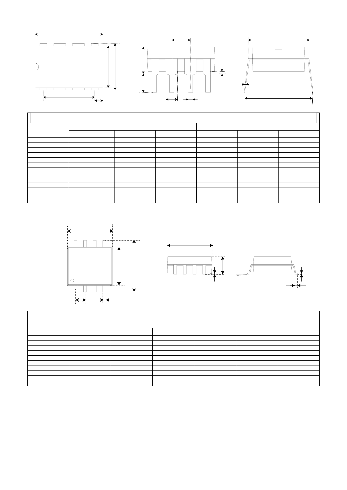
Pin 1
M
SYMBOL
F
A
S1
a
A
r
S
L2
x
m
Q
L1 L
Package type: 8-pin Dual-In-Line
InchesMillimeters
0.280.247.116.1a
0.3250.38.267.62A
0.40.35510.169.02M
0.0370.0270.940.69Q
0.0220.0140.5590.356L
0.070.0451.781.14L1
0.0120.0080.3050.203L2
-0.015-0.38r
0.150.1153.812.92S
0.21-5.33-S1
0.4310.9x
NotesMaxMinNotesMaxMin
Typical-0.3Typical-7.62m
BSC-0.1BSC-2.54F
Pin 1
SYMBOL
φ
M
M
a
A
H
φ
h
e
E
Package type: 8-pin Wide SOIC
InchesMillimeters
0.2130.2055.415.21a
0.330.38.387.62A
0.2120.2035.385.16M
0.020.0120.5080.305L
0.0130.0040.330.102h
0.080.072.031.78H
0.010.0070.2540.178e
0.0350.020.8890.508E
o
0
o
8
o
0
o
8
NotesMaxMinNotesMaxMin
BSC0.05BSC1.27F
LQ
11
QT300 R1.01 21/09/03

lQ
Copyright © 2002 QRG Ltd. All rights reserved.
Patented and patents pending
Corporate Headquarters
1 Mitchell Point
Ensign Way, Hamble SO31 4RF
Great Britain
Tel: +44 (0)23 8056 5600 Fax: +44 (0)23 8045 3939
admin@qprox.com
www.qprox.com
North America
651 Holiday Drive Bldg. 5 / 300
Pittsburgh, PA 15220 USA
Tel: 412-391-7367 Fax: 412-291-1015
The specifications set out in this document are subject to change without notice. All products sold and services supplied by QRG are subject
to our Terms and Conditions of sale and supply of services which are available online at www.qprox.com and are supplied with every order
acknowledgement. QProx, QTouch, QMatrix, QLevel, and QSlide are trademarks of QRG. QRG products are not suitable for medical
(including life-saving equipment), safety or mission critical applications or other similar purposes. Except as expressly set out in QRG's
Terms and Conditions, no licenses to patents or other intellectual property of QRG (express or implied) are granted by QRG in connection
with the sale of QRG products or provision of QRG services. QRG will not be liable for customer product design and customers are entirely
responsible for their products and applications which incorporate QRG's products.
 Loading...