

APPLICATIONS -
!
Elevator buttons
!
Toys & games
!
Access systems
!
Pointing devices
!
Appliance control
!
Security systems
!
Light switches
!
Prox sensors
The QT113 charge-transfer (“QT’”) touch sensor is a self-contained digital IC capable of detecting near-proximity or touch. It will
project a proxim it y sense field through air , via al m ost any dielectric, li ke glass, pl asti c, stone, cerami c, and m ost kinds of wood. It can
also turn sm all m etal -bearing objects into i ntri nsic sensors, m aking them r esponsive to proximi ty or touch. Thi s capability coupled with
its ability to self calibrate continuously can lead to entirely new product concepts.
It is designed specifically for human interfaces, like control panels, appliances, toys, lighting controls, or anywhere a mechanical
switch or button m ay be found; it m ay also be used for some material sensing and control appl ications provided that t he presence
duration of objects does not exceed the recalibration timeout interval.
The QT113 requires only a common inexpensive capacitor in order to function.
Power consumption is only 600µA in most applications. I n most cases the power supply need only be minim al ly regulated, for example
by Zener diodes or an inexpensive 3-terminal regulator.
The QT113’s RISC core employs signal processing techniques pioneered by Quantum ; these are specifically designed to make the
device survive real-world challenges, such as ‘stuck sensor’ conditions and signal drift. Even sensitivity is digitally determined and
remains const ant in the face of large variations in sample capacitor C
S
and electrode CX. No external switches, opamps, or other
analog components aside from C
S
are usually required.
The option-selectable toggle mode perm its on/off touch contr ol, for example for li ght switch replacement. The Quantum-pi oneered
HeartBeat™ signal is also incl uded, allowing a host m icrocontroller to m onitor the health of the QT113 continuously if desired. By
using the charge transfer principle, the IC delivers a level of performance clearly superior to older technologies in a highly
cost-effective package.
Quantum Research Group Ltd
Copyright Quantum Research Group Ltd
R1.10/0104
!
!!
! Projects a proximity field through air
!
!!
! Less expensive than many mechanical switches
!
!!
! Sensitivity easily adjusted via capacitor value
!
!!
! Turns small objects into intrinsic touch sensors
!
!!
! 100% autocal for life - no adjustments required
!
!!
! 2.5 to 5V, 600µµµµA single supply operation
!
!!
! Toggle mode for on/off control (strap option)
!
!!
! 10s, 60s, infinite auto-recal timeout (strap options)
!
!!
! Gain settings in 2 discrete levels
!
!!
! HeartBeat™ health indicator on output
!
!!
! Active-low (QT113) or active-high outputs (QT113H)
!
!!
! Only one external part required - a 1¢ capacitor
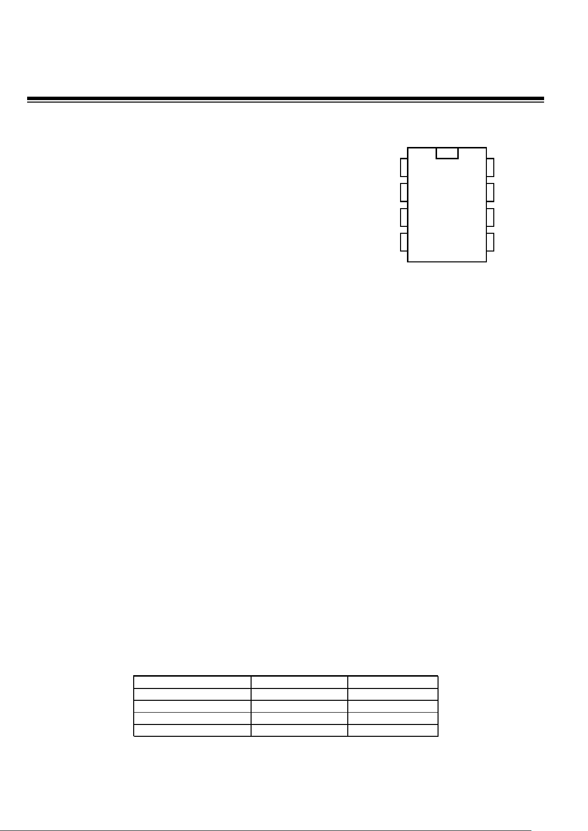
QProx™™™™ QT113 / QT113H
C
HARGE-TRANSFER TOUCH SENSO
R
Sn s2
Vss
Sn s1
GainOpt2
Opt1
Out
Vdd 1
2
3
45
6
7
8
QT113
-
QT113H-IS-400C to +850C
-
QT113-IS-400C to +850C
QT113H-DQT113H-S0
0
C to +700C
QT113-DQT113-S0
0
C to +700C
8-PIN DIPSOICT
A
AVAILABLE OPTIONS
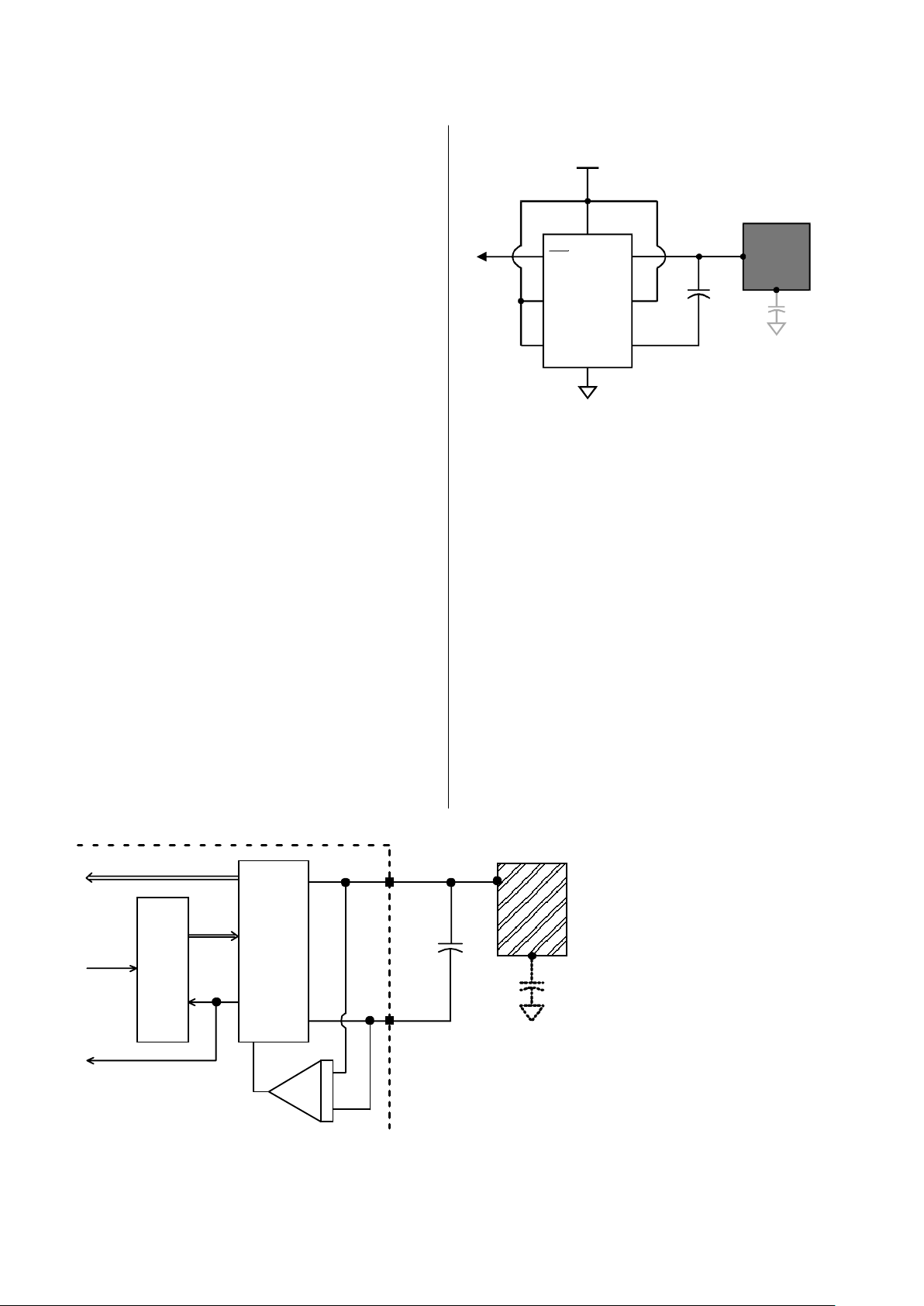
1 - OVERVIEW
The QT113 is a digital burst mode charge-transfer (QT)
sensor designed specifically for touch controls ; it incl udes all
hardware and signal processing functions necessary to
provide stable sensing under a wide variety of changing
conditions. Only a single low cost, non-critical capacitor is
required for operation.
Figure 1-1 shows the basic Q T113 circuit using the device,
with a conventional output drive and power supply
connections.
1.1 BASIC OPERATION
The QT113 employs bursts of charge-transfer cycles to
acquire its signal. Burst mode permits power consumption in
the microamp range, dramatically reduces RF emissions,
lowers susceptibility to EMI, and yet permits excellent
response time. Internally the signals are digitally processed
to reject impulse noise, using a 'consensus' filter which
requires three consecutive confirmations of a detection
before the output is activated.
The QT switches and charge measurement hardware
functions are all i nternal to the QT113 (Figure 1-2). A 14-bi t
single-slope switched capacitor ADC includes both the
required QT charge and transfer switches in a configurati on
that provides direct ADC conversion. The ADC is designed to
dynamically optimize the QT burst length according to the
rate of charge buildup on Cs, which in turn depends on the
values of Cs, Cx, and Vdd. Vdd is used as the charge
reference voltage. Larger values of Cx cause the charge
transferred into Cs to rise more rapidly, reducing available
resolution; as a minimum resolution is required for proper
operation, this can result in dramatically reduced apparent
gain. Conversely, larger values of Cs reduce the rise of
differential voltage across it, increasing available resolution
by permitti ng longer QT bursts. The value of Cs can thus be
increased to allow larger values of Cx to be tolerated (Figures
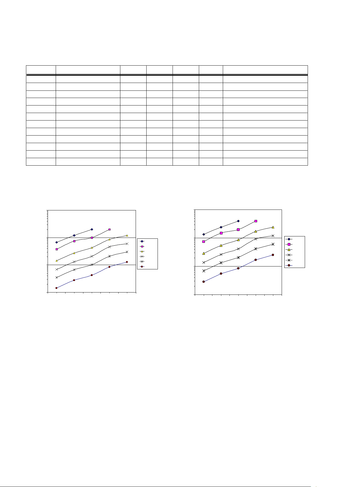
4-1, 4-2, 4-3 in Specifications, rear).
The IC is responsive to both Cx and Cs, and changes in Cs
can result in substantial changes in sensor gain.
Option pins allow the selection or alteration of several special
features and sensitivity.
1.2 ELECTRODE DRIVE
The internal ADC treats Cs as a floating t r ansf er capacitor; as
a direct result, the sense electrode can be connected to
either SNS1 or SNS2 with no performance difference. In both
cases the rule Cs >> Cx must be observed for proper
operation. The polarity of the charge buildup across Cs
during a burst is the same in either case.
It is possibl e to connect separate Cx and Cx’ loads to SNS1
and SNS2 simul taneously, although the result i s no diff erent
than if the loads were connected together at SNS1 (or
SNS2). It is i mportant t o lim i t the amount of st r ay capacitance
on both term inals, especially if t he load Cx is already large,
for example by mini m izing tr ace lengths and widths so as not
to exceed the Cx load specificat ion and to allow for a larger
sensing electrode size if so desired.
The PCB traces, wiring, and any components associated with
or in contact with SNS1 and SNS2 will become touch
sensitive and should be treated with caution to li m it t he touch
area to the desired location. Multiple touch electrodes can be
used, for example to create a control button on bot h sides of
an object, however it is impossible for the sensor to
distinguish between the two touch areas.
1.3 ELECTRODE DESIGN
1.3.1 E
LECTRODE GEOMETRY AND SIZE
There is no restriction on the shape of
the electrode; in most cases common
sense and a little experimentation can
result in a good electrode design. The
QT113 will operate equally well with
long, thin electrodes as with round or
square ones; even random shapes are
acceptable. The electrode can also be
a 3-dimensional surface or object.
Sensitivity is related to electrode
surface area, orientation with respect
to the object being sensed, object
composition, and the ground coupling
quality of both the sensor circuit and
the sensed object.
If a rel ati vel y la rge el ectr ode s urf ac e is
desired, and if tests show that the
electrode has more capacitance than
the QT113 can tolerate, the electrode
- 2 -
Figure 1-1 Standard mode options
SENSING
ELECTRODE
C
s
10nF
3
46
5
1
+
2
.5 to 5
72
OUT
OPT1
OPT2
GAIN
SNS1
SNS2
Vss
Vdd
OUTPUT=DC
TIMEOUT=10 Secs
TOGGLE=OFF
GAIN=HIGH
C
x
8
Figure 1-2 Internal Switching & Timing
C
s
C
x
SNS2
SNS1
ELECTRODE
Single-Slope 14-bit
Switched Capacitor ADC
Charge
Amp
Burst Controller
Result
Don e
Start
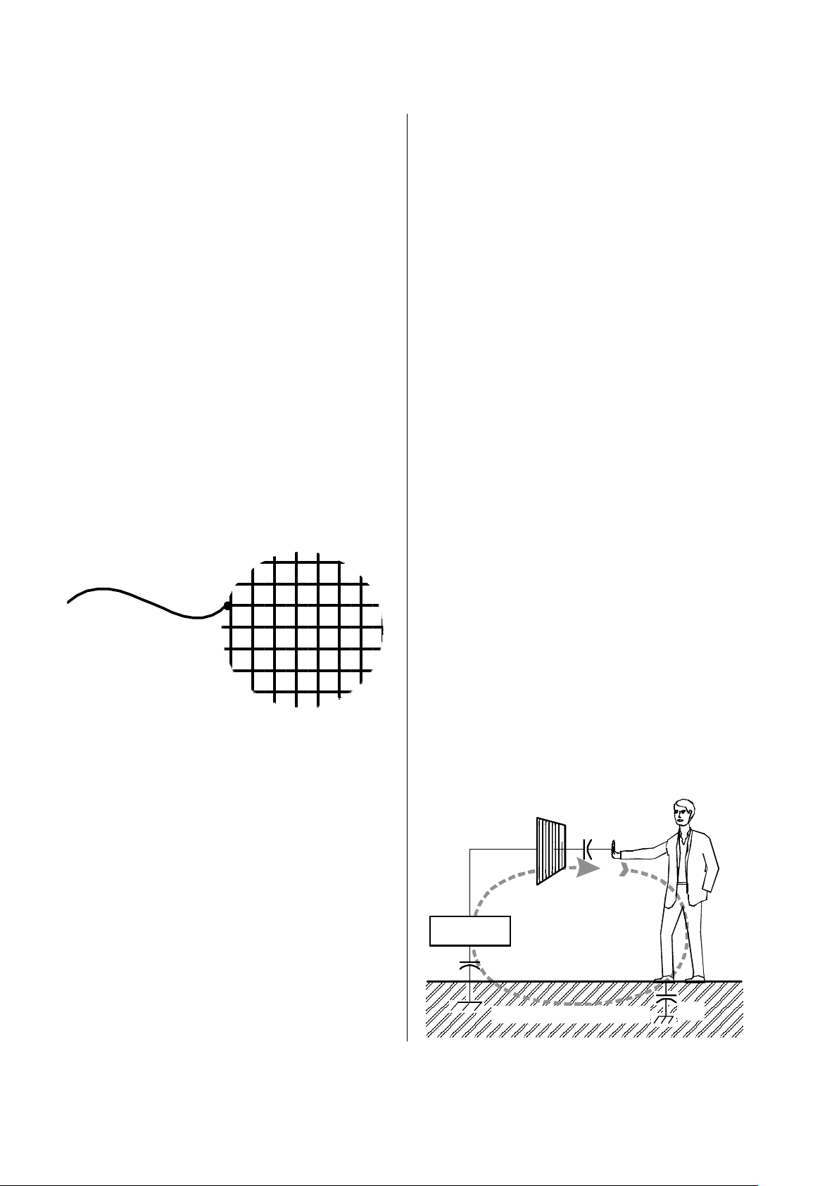
can be made into a sparse mesh (Figure 1-3) havi ng lower
Cx than a solid plane. Sensitivity m ay even remain the same,
as the sensor will be operating in a lower region of the gain
curves.
1.3.2 K
IRCHOFF’S CURRENT LAW
Like all capacitance sensors, the QT113 relies on Kirchoff’s
Current Law (Figure 1-4) to detect the change in capacit ance
of the electrode. This law as applied to capacitive sensing
requires that the sensor’s field current must complete a loop,
returning back to its source in order for capacitance to be
sensed. Although most designers relate to Kirchoff’s law wit h
regard to hardwired circuits, it applies equally to capacitive
field flows. By implication it requires that the signal ground
and the target object must bot h be coupled together in some
manner for a capaci ti ve sensor to operate properly. Note that
there is no need to provide actual hardwired ground
connections; capacitive coupling to ground (Cx1) is always
sufficient, even if the coupling might seem very tenuous. For
example, powering the sensor via an isolated transform er will
provide ample ground coupling, since there is capacitance
between the windings and/or the transform er core, and from
the power wiring itself directly to 'local earth'. Even when
battery powered, just the physical size of the PCB and the
object into which the electronics is embedded will generally
be enough to couple a few picofarads back to local earth.
1.3.3 V
IRTUAL CAPACITIVE GROUNDS
When detecting human contact (e.g. a fingertip), grounding
of the person is never required. The human body naturally
has several hundred picofarads of ‘free space’ capacitance to
the local environment (Cx3 in Figur e 1-4), which i s m ore than
two orders of m agnitude greater than that requir ed to create
a return path to the QT113 via earth. The QT113's PCB
however can be physically quite sm all, so there may be little
‘free space’ coupling (Cx1 in Figure 1-4) between it and t he
environment to com plete the return path. If t he QT113 circuit
ground cannot be earth grounded by wire, for example via
the supply connections, then a ‘virtual capacitive ground’ may
be required to increase return coupling.
A ‘virtual capacit i v e ground’ can be created by connecting the
QT113’s own circuit ground to:
(1) A nearby piece of metal or metallized housing;
(2) A floating conductive ground plane;
(3) A nail driven into a wall;
(4) A larger electronic device (to which its output might be
connected anyway).
Free-floating ground planes such as metal foils should
maximi ze exposed surface area in a flat plane if possible. A
square of metal foil will have little effect if it is rolled up or
crumpled into a bal l. Virt ual ground pl anes are mor e effective
and can be made smaller if they are physically bonded to
other surfaces, for example a wall or floor.
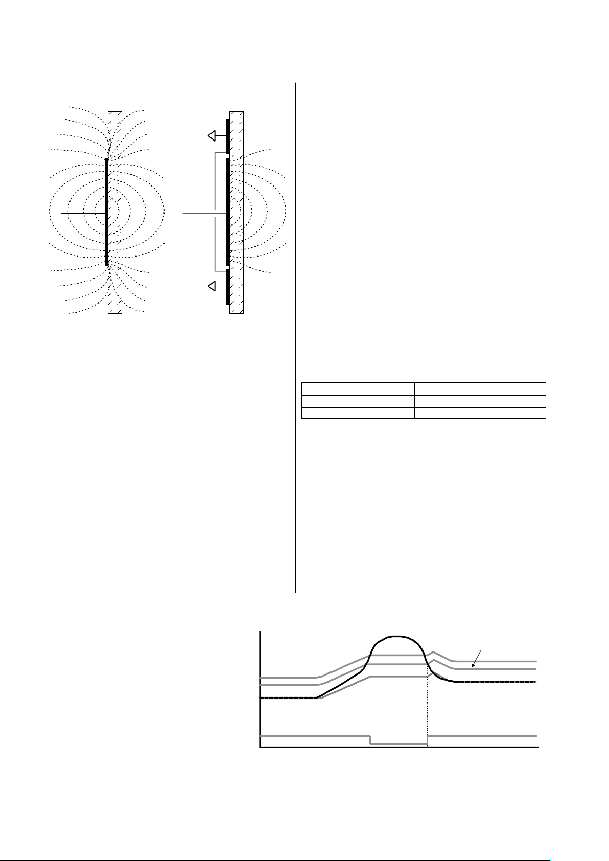
1.3.4 F
IELD SHAPING
The electrode can be prevented from sensing in undesired
directions with the assistance of metal shielding connected to
circuit gr ound ( Figure 1-5). For example, on f lat sur faces, the
field can spread laterally and create a larger touch area than
desired. To stop field spreading, it is only necessary to
surround the touch electrode on all sides with a ring of metal
connected to circuit ground; the ring can be on the same or
opposite side from the electrode. The ring will kill field
spreading from that point outwards.
If one side of the panel to which the electrode is fixed has
moving traffic near it, these objects can cause inadvertent
detections. This is cal led ‘walk-by’ and is caused by the fact
that the fields radiate from either surface of the electrode
equally well. Again, shieldi ng in the form of a metal sheet or
foil connected to circ uit ground will prevent walk-by; putting a
small ai r gap between the grounded shield and the electrode
will keep the value of Cx lower and is encouraged. In the
case of the QT113, sensitivity can be high enough
(depending on Cx and Cs) that 'walk-by' signals are a
concern; if this is a probl em , then some form of rear shieldi ng
may be required.
1.3.5 S
ENSITIVITY
The QT113 can be set for one of 2 gain levels using option
pin 5 (Table 1-1). This sensiti vity change i s made by alt ering
the internal num eri cal threshold level required for a detection.
Note that sensitivity is also a functi on of other things: like the
value of Cs, electrode size, shape, and orientation, the
composition and aspect of the object to be sensed, the
thickness and composi tion of any overlaying panel m aterial,
and the degree of ground coupling of both sensor and object.
1.3.5.1 Increasing Sensitivity
In some cases it may be desirable to increase sensitivity
further, for example when using the sensor with very thick
panels having a low dielectric constant.
Sensitivity can often be increased by using a bigger
electrode, reducing panel thickness, or altering panel
compositi on. Increasing electrode size can have diminishi ng
returns, as high values of Cx will reduce sensor gain (Figures
- 3 -
Figure 1-3 Mesh Electrode Geometry
Figure 1-4 Kirchoff's Current Law
Sense Electrode
C
X2
Surround ing e nv ironm en t
C
X3
SENSOR
C
X1
4-1 to 4-3). The value of Cs also has a dram atic effect on
sensitivity, and t his can be increased in value (up to a limit ).
Also, increasing the electrode's surface area will not
substantially increase touch sensitivity if its diameter is
already much larger in surface area than the object being
detected. The panel or other intervening material can be
made thinner, but again there are diminishing rewards for
doing so. Panel material can also be changed to one having
a higher dielectric constant, which will help propagate the
field through to the front. Locally adding some conductive
material to the panel (conductive materials essentially have
an infinite dielectric constant) will also help; for example,
adding carbon or metal fibers to a plastic panel will greatly
increase frontal fi eld strength, even if the fiber density is too
low to make the plastic bulk-conductive.
1.3.5.2 Decreasing Sensitivity
In some cases the QT113 may be too sensitive, even on low
gain. In thi s case gain can be lowered further by a num ber of
strategies: making the electrode smaller, making the
electrode into a sparse mesh using a high
space-to-conductor ratio (Figure 1-3), or by decreasing Cs.
2 - QT113 SPECIFICS
2.1 SIGNAL PROCESSING
The QT113 processes all signals using 16 bit
math, usi ng a number of algorithm s pioneered by
Quantum. The algorithms are specifically
designed to provide for high 'survivability' in the
face of numerous adverse environmental
changes.
2.1.1 D
RIFT COMPENSATION ALGORITHM
Signal drift can occur because of changes in Cx
and Cs over time. It is crucial that drift be
compensated for, otherwise false detections,
non-detections, and sensitivity shifts will follow.
Drift com pensation (Figur e 2-1) is perform ed by making t he
reference level track the raw signal at a slow rate, but only
while there is no detection in effect. The rate of adjustment
must be performed slowly, otherwise legitimate detections
could be ignored. The QT113 drift compensates using a
slew-rate limit ed change to the reference level; the threshold
and hysteresis values are slaved to this reference.
Once an object is sensed, the drift compensation mechanism
ceases since the signal is legitimately high, and therefore
should not cause the reference level to change.
The QT113's drift compensation is 'asymmetric': the
reference level drift-com pensates in one direction faster than
it does in the other. Specifically, it compensates faster for
decreasing signals than for increasing signals. Increasing
signals should not be compensated for quickly, since an
approaching finger could be compensated for partially or
entirely before even approaching the sense electrode.
However, an obstruction over the sense pad, for which the
sensor has already made full all owance for, could suddenly
be removed leaving the sensor with an artificially elevated
reference level and thus become insensitive to touch. In this
latter case, the sensor will compensate for the object's
removal very quickly, usually in only a few seconds.
With large values of Cs and small values of Cx, drift
compensation will appear to operate more slowly than with
the converse.
Note that the positive and negative drift
compensation rates are different.
2.1.2 T
HRESHOLD CALCULATION
Unlike the QT110 device, the internal threshold level is fixed
at one of two setting as determined by Table 1-1. These
setting are fixed with respect to the internal reference level,
which in turn can move in accordance with the drift
compensation mechanism..
The QT113 employs a hysteresis dropout below the
threshold level of 17% of the delta between the reference and
threshold levels.
2.1.3 MAX ON-D
URATION
If an object or material obstructs the sense pad the signal
may rise enough to create a detection, preventing further
- 4 -
Figure 1-5
Shielding Against Fringe Fields
Sense
wire
Sense
wire
Unshielded
Shielded
Figure 2-1 Drift Compensation
Threshold
Signal
Hysteresis
Reference
Output
Vss (Gnd)
Low - 12 counts
Vdd
High - 6 counts
Tie Pin 5 to:Gain
Table 1-1 Gain Setting Strap Options

operation. To prevent this, the sensor includes a tim er which
monitors detections. If a detection exceeds the timer setting,
the timer causes the sensor to perform a full recalibration
(when not set to infinite). This is known as the Max
On-Duration feature.
After the Max On-Duration interval, the sensor will once again
function norm ally, even if partially or fully obstructed, to t he
best of its ability given electrode conditions. There are two
finite tim eout durations available via strap option: 10 and 60
seconds (Table 2-1).
2.1.4 D
ETECTION INTEGRATOR
It is desirable t o suppress detections generated by electrical
noise or from quick brushes with an object. To accomplish
this, the Q T113 incorpor ates a detect integrati on counter that
increments with each detection until a limit i s reached, after
which the output is acti vated. If no detection is sensed prior
to the final count, the counter is reset immediately to zero. In
the QT113, the required count is 3.
The Detection I nt egrator can also be viewed as a 'consensus'
filter, that r equires three detections in three successive bursts
to create an output.
2.1.5 F
ORCED SENSOR RECALIBRATION
The QT113 has no recalibration pin; a forced recalibrat ion is
accomplished only when the device is powered up. However,
supply drain is l ow so it is a simpl e matter to treat the entire
IC as a controllabl e load; sim ply drivi ng the QT113's Vdd pin
directly from another logic gate or a microcontroller port
(Figure 2-2) will serve as both power and 'forced recal'. The
source resistance of most CMOS gates and microcont rollers
are low enough to provide direct power without pr oblem. Note
that most 8051-based micros have only a weak pullup drive
capability and will require CMOS buffering. 74HC or 74AC
series gates can directly power the QT113, as can most ot her
microcontrollers.
Option strap configurations are read by the QT113 only on
powerup. Configurations can only be changed by powering
the QT113 down and back up again; again, a mi crocontrol ler
can directly alter m ost of the configurati ons and cycle power
to put them in effect.
2.1.6 R
ESPONSE TIME
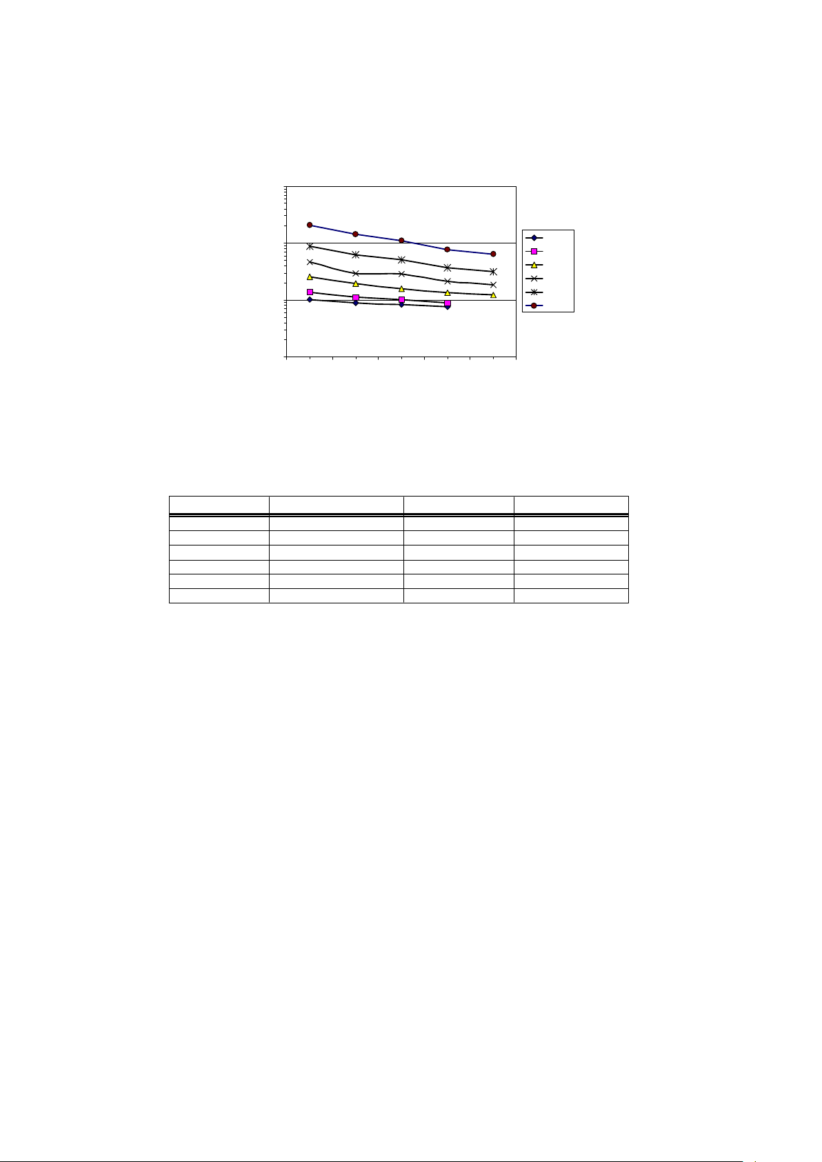
The QT113's response time is highly dependent on burst
length, which in turn i s dependent on Cs and Cx (see Figures
4-1, 4-2). With increasing Cs, response time slows, while
increasing levels of Cs reduce response time. Figure 4-3
shows the typical effects of Cs and Cx on response time.
2.2 OUTPUT FEATURES
The QT113 is designed for maximum flexibility and can
accommodate most popular sensing requirements. These
are selectable using strap options on pins OPT1 and OPT2.
All options are shown in Table 2-1.
2.2.1 DC M
ODE OUTPUT
The output of the QT113 can respond i n a DC mode, where
the output is active-low upon detection. The output will
remain active-low for the duration of the detection, or unt i l the
Max On-Duration expires (if not infinite), whichever occurs
first. If a max on-duration timeout occurs first, the sensor
performs a ful l recali bration and the output becom es inactive
until the next detection.
In this m ode, three Max On-Duration tim eouts are available:
10 seconds, 60 seconds, and infinite.
Infinite timeout is useful in applications where a prolonged
detection can occur and where the output must reflect the
detection no matter how long. In infinite timeout mode, the
designer should take care to be sure that drift in Cs, Cx, and
Vdd do not cause the device to ‘stick on’ inadvertently even
when the target object is removed from the sense field.
2.2.2 T
OGGLE MODE OUTPUT
This makes the sensor respond in an on/off mode like a flip
flop. I t i s m ost useful for cont roll ing power l oads, f or example
in kitchen appliances, power tools, light switches, etc.
Max On-Duration in Toggle mode is fixed at 10 seconds.
When a timeout occurs, the sensor recalibrates but leaves
the output state unchanged.
2.2.3 H
EARTBEAT
™ O
UTPUT
The QT113 output has a full-time HeartBeat™ ‘health’
indicator superimposed on it. This operates by taking 'Out'
into a 3-state mode for 300µs once after every QT burst. This
output state can be used to determine that the sensor is
operating properly, or, i t can be ignored using one of several
simple methods.
The HeartBeat indicator can be sampled by usi ng a pull down
resistor on Out, and feeding the resulting negative-going
pulse into a counter, f lip fl op, one-shot, or other cir cuit. Since
Out is normally high, a pulldown resistor will create negative
HeartBeat pulses (Figure 2-3) when the sensor is not
detecting an object; when detecting an object, the output will
remain low for the duration of the detection, and no
HeartBeat pulse will be evident.
If the sensor is wired to a m icrocontr oller as shown in Figure
2-4, the microcontroller can reconfigure the load resistor to
either ground or Vcc depending on the output state of the
QT113, so that the pulses are evident in either state.
- 5 -
infiniteVddGnd
DC Out
10sGndGnd
Toggle
60sGndVdd
DC Out
10sVddVdd
DC Out
Max On-
Duration
Tie
Pin 4 to:
Tie
Pin 3 to:
Table 2-1 Output Mode Strap Options
Figure 2-2 Powering From a CMOS Port Pin
0.01µF
CMO S
microcontroller
OUT
PORT X.m
PORT X.n
Vdd
Vss
QT110

Electromechanical devices like relays will usually ignore this
short pulse. The pulse also has too low a duty cycle to visibly
affect LED’s. It can be filtered completely if desired, by
adding an RC timeconstant to fil t er the output, or if int erfaci ng
directly and only to a high-i mpedance CMOS input, by doing
nothing or at m ost adding a sm all non-crit ical capacit or from
Out to ground (Figure 2-5).
The QT113H variant has an active-high output; the heartbeat
signal of the QT113H works in exactly the same manner.
2.2.4 O
UTPUT DRIVE
The QT113’s `output is active low and can sink up to 5mA of
non-inductive current. If an inducti ve load is used, such as a
small relay, the load should be diode clamped to prevent
damage. When set to operate in a proximity mode (at high
gain) the current should be limited to 1mA to prevent gain
shifting si de effects from occur ring, which happens when the
load current creates voltage drops on the die and bonding
wires; these small shifts can materially influence the signal
level to cause detection instability as described below.
Care should be taken when the QT113 and the load are both
powered from the same suppl y, and the supply is m inimall y
regulated. The QT113 derives its internal references from the
power supply, and sensitivity shifts can occur with changes in
Vdd, as happens when loads are switched on. This can
induce detection ‘cycling’, whereby an object is detected, the
load is turned on, the supply sags, t he detection is no longer
sensed, the load is turned off, the supply rises and the object
is reacquired, ad infinitum. To prevent this occurrence, the
output should only be lightl y loaded if the device is operated
from an unregulated supply, e.g. batteries. Detection
‘stiction’, the opposite effect, can occur if a load is shed when
Out is active.
The output of the QT113 can directly drive a resistively
limi ted LED. The LED should be connected with its cathode
to the output and it s anode towards Vcc, so that it l ights when
the sensor is active. If desired the LED can be connected
from Out to ground, and driven on when the sensor is
inactive.
The QT113H variant has an active-high output.
3 - CIRCUIT GUIDELINES
3.1 SAMPLE CAPACITOR
Charge sampler Cs can be virtually any plastic film or
medium-K ceramic capacitor. The acceptable Cs range is
from 10nF to 500nF depending on the sensitivity required;
larger values of Cs demand higher stability to ensure reliable
sensing. Acceptable capacitor types include polycarbonate,
PPS film, or NPO/C0G ceramic.
3.2 OPTION STRAPPING
The option pins Opt1 and Opt 2 should never be left floating.
If they are floated, the device will draw excess power and the
options will not be properly read on powerup. Intentionally,
there are no pullup resistors on these lines, since pullup
resistors add to power drain if tied low.
The Gain input should be connected to either Vdd or Gnd.
Tables 1-1 and 2-1 show the option strap configurations
available.
3.4 POWER SUPPLY, PCB LAYOUT
The power supply can range from 2.5 to 5.0 volts. At 3 volts
current drain averages less than 600µA in most cases, but
can be higher if Cs is large. Increasing Cx values will actually
decrease power drain. Operation can be from batteries, but
be cautious about loads causing supply droop (see Output
Drive, previous section).
As battery voltage sags with use or fluctuates slowly with
temperature, the QT113 will track and compensate for these
changes automatically with only minor changes in sensitivity.
If the power supply is shared with another electronic system,
care should be taken to assure that the supply is free of
- 6 -
Figure 2-4
Using a micro to obtain HB pulses in either output state
Figure 2-3
Getting HearBeat pulses with a pull-down resistor
3
46
5
1
+2.5 to 5
72
OUT
OPT1
OPT2
GAIN
SNS1
SNS2
Vss
Vdd
8
Ro
HeartBeat™ Pulses
Microcontroller
PORT_M.x
PORT_M.y
3
46
5
72
OUT
OPT1
OPT2
GAIN
SNS1
SNS2
R
o
Figure 2-5 Eliminating HB Pulses
3
46
5
72
OUT
OPT1
OPT2
GAIN
SNS 1
SNS 2
CMOS
100pF
C
o
GATE OR
MICRO INPUT

digital spikes, sags, and surges which can adversely affect
the QT113. The QT113 will track slow changes in Vdd, but it
can be affected by rapid voltage steps.
if desired, the supply can be regulated using a conventional
low current regulator, f or example CMOS regulators that have
low quiescent currents.
3.5 ESD PROTECTION
In cases where the electrode is placed behind a dielectric
panel, the QT113 will usually be adequately protected from
direct static discharge. However, even with a plastic or glass
panel, transients can still flow into the electrode via induction,
or in extreme cases, via dielectric breakdown. Porous
materials may allow a spark to tunnel right through the
material; partially conducting materials like 'pink poly' will
conduct the ESD right to the electrode. Testing is required to
reveal any problems. The QT113 does have diode protection
on its termi nals which can absorb and prot ect the device from
most induced discharges, up to 20m A; the usefulness of the
internal clamping will depending on the dielectric properties,
panel thickness, and rise time of the ESD transients.
ESD dissipation can be aided further with an added diode
protection network as shown in Figur e 3-1, i n extreme cases.
Because the charge and transfer times of the QT113
are relatively long, the circuit can tolerate very large
values of Re, even to 100k ohms in most cases where
electrode Cx is small. The added diodes shown
(1N4150 or equivalent low-C diodes, or a singl e BAV99
dual-diode) will shunt the ESD transients away f r om the
part, and Re1 will current limit the rest into the QT113's
own internal clam p diodes. C1 should be around 10µF
if it is to absor b positive transients from a hum an body
model standpoint wi thout r isi ng in val ue by more than 1
volt. If desired C1 can be replaced with an appropriate
Zener diode. Directly placing semiconductor transient
protection devices, Zeners, or MOV's on the sense lead
is not advised; these devices have extremely large
amounts of unst able parasitic C which will swamp the
QT113 and render it useless.
Re1 should be as large as possible given the load
value of Cx and the diode capacitances of D1 and D2,
but Re1 should be low enough to permit at least 6
timeconstants of RC to occur during the charge and transfer
phases.
Re2 functions to isol ate the transient from t he QT113's Vdd
pin; values of around 1K ohms are reasonable.
As with all ESD protection networks, it is crucial that the
transients be led away from the circui t. PCB ground layout i s
crucial; the ground connections to D1, D2, and C1 shoul d all
go back to the power supply ground or preferably, if
available, a chassis ground connected to earth. The currents
should not be allowed to traverse the area directly under the
QT113.
If the QT113 is connected to an external circuit vi a a cable or
long twisted pair, it is possible for ground-bounce to cause
damage to the Out pin; even though the transients are led
away from the QT113 itself, the connected signal or power
ground line will act as an inductor, causing a hi gh differential
voltage to build up on the Out wire with respect to ground. If
this is a possibility, the Out pin should have a resistance Re3
in series with it to limit current; this resistor should be as
large as can be tolerated by the load.
- 7 -
Figure 3-1 ESD Suppression Circuit
3
46
5
1
+2.5 to 5
72
OUT
OPT1
OPT2
GAIN
SNS1
SNS2
Vss
Vdd
8
R
C
D
D
R
R
e3
s
2
1
e2
e1
SENS IN G
ELEC TRO D E
10µF
+
C1

4.1 ABSOLUTE MAXIMUM SPECIFICATIONS
Operating temp ............................................................ as designated by suffix
Storage temp ................................................................... -55
O
C to +125OC
V
DD
...............................................................................-0.5 to +6.5V
Max continuous pin current, any control or drive pin ............................................ ±20mA
Short circuit duration to ground, any pin ....................................................... infinite
Short circuit duration to V
DD
, any pin ......................................................... infinite
Voltage forced onto any pin ................................................. -0.6V to (Vdd + 0.6) Volts
4.2 RECOMMENDED OPERATING CONDITIONS
VDD ............................................................................... +2.5 to 5.5V
Short-term supply ripple+noise ...............................................................±5mV
Long-term supply stability ................................................................ ±100mV
Cs value ......................................................................... 10nF to 500nF
Cx value ............................................................................ 0 to 100pF
4.3 AC SPECIFICATIONS
Vdd = 3.0, Ta = recommended operating range
, Cs=100nF unless noted
µs300Heartbeat pulse widthT
HB
Cx = 10pF; See Figure 4-3ms30Response timeT
R
Cs = 10nF to 500nF; Cx = 0ms750.5Burst lengthT
BL
Cs = 10nF to 500nF; Cx = 0ms802.1Burst spacing intervalT
BS
µs2Transfer durationT
PT
µs2Charge durationT
PC
ms550Recalibration timeT
RC
NotesUnitsMaxTypMinDescriptionParameter
4.4 SIGNAL PROCESSING
Option pin selectedsecs10, 60, infinitePost-detection recalibration timer duration
ms/level100Negative drift compensation rate
ms/level1,000Positive drift compensation rate
samples3Consensus filter length
Note 1%17Hysteresis
Option pin selectedcounts6 or 12Threshold differential
NotesUnitsMaxTypMinDescription
Note 1: Percentage of signal threshold
- 8 -
4.5 DC SPECIFICATIONS
Vdd = 3.0V, Cs = 10nF, Cx = 5pF, TA = recommended range, unless otherwise noted
Note 2fF281,000Sensitivity rangeS
bits14Acquisition resolutionA
R
Resistance from SNS1 to SNS2
✡
1MMin shunt resistanceI
X
pF1000Load capacitance rangeC
X
OPT1, OPT2µA±1Input leakage currentI
IL
OUT, 1mA sourceVVdd-0.7High output voltageV
OH
OUT, 4mA sinkV0.6Low output voltageV
OL
OPT1, OPT2V2.2High input logic levelV
HL
OPT1, OPT2V0.8Low input logic levelV
IL
Required for proper startupV/s100Supply turn-on slopeV
DDS
µA1,500600Supply currentI
DD
V5.252.45Supply voltageV
DD
NotesUnitsMaxTypMinDescriptionParameter
Note 2: Sensitivity depends on value of Cx and Cs. Refer to Figures 4-1, 4-2.
- 9 -
Figure 4-1 - Typical Threshold Sensitivity vs. Cx,
High Gain, at Selected Values of Cs; Vdd = 3.0
0.01
0.10
1.00
10.00
0 10203040
Cx Load, pF
Detection Threshold, pF
10nF
20nF
50nF
100nF
200nF
500nF
Figure 4-2 - T ypical Thres hold Sensitivity vs. Cx,
Low Gain, at Selected Values of Cs; Vdd = 3. 0
0.01
0.10
1.00
10.00
0 10203040
Cx Load, pF
Detection Threshold, pF
10nF
20nF
50nF
100nF
200nF
500nF
5 ORDERING INFORMATION
QT1 + KSOIC-8-40 - 85CQT113H-IS
QT1 + ESOIC-80 - 70CQT113H-S
QT1 + 13HPDIP0 - 70CQT113H-D
QT1 + FSOIC-8-40 - 85CQT113-IS
QT1 + 3SOIC-80 - 70CQT113-S
QT1 + 13PDIP0 - 70CQT113-D
MARKINGPACKAGETEMP RANGEPART
- 10 -
Chart 4-3 - Typical Response Time vs. Cx;
Vdd = 3.0
1.00
10.00
100.00
1000.00
0 10203040
Cx Load
Response Time, ms
10nF
20nF
50nF
100nF
200nF
500nF

0.0150.0080.3810.203Y
0.390.329.9068.128x
BSC0.30.3BSC7.0627.62Aa
0.16-4.064-S1
0.140.123.5563.048S
-0.015-0.381r
0.150.123.813.048R
Typical0.1020.098Typical2.5912.489F
0.0650.0551.6511.397L1
0.0220.0140.5590.355L
-0.01-0.254P
-0.035-0.889Q
BSC0.30.3BSC7.627.62m
Typical0.430.355Typical10.9229.017M
0.3250.38.2557.62A
0.280.247.112 6.096a
NotesMaxMinNotesMaxMin
InchesMillimeters
SYMBOL
Package type: 8-pin Dual-In-Line
8º0º8º0ºØ
0.030.2290.7620.381ß
0.010.0070.2490.19e
0.040.021.0160.508E
0.0190.0140.4830.355L
BSC0.050.050BSC1.271.27D
0.010.0040.7620.101h
0.0680.0541.7281.371H
0.1570.153.9883.81Aa
0.2440.2296.1985.816W
0.1960.1894.9794.800M
NotesMaxMinNotesMaxMin
InchesMillimeters
SYMBOL
Package type: 8-pin SOIC
- 11 -

Quantum Research Group Ltd
©2001QRG Ltd.
Patented and patents pending
651 Holiday Drive Bldg. 5 / 300
Pittsburgh, PA 15220 USA
Tel: 412-391-7367 Fax: 412-291-1015
admin@qprox.com
http://www.qprox.com
In the United Kingdom
Enterprise House, Southampton, Hants SO14 3XB
Tel: +44 (0)23 8045 3934 Fax: +44 (0)23 8045 3939
This device expressly not for use in any medical or human safety related
application without the express written consent of an officer of the company.
 Loading...