PYRAMID PYX28C64 Technical data

1
Document # EEPROM101 REV B
Revised July 2007
FEATURES
Access Times of 200, 250, 300 and 350 ns
Single 5V±10% Power Supply
Simple Byte and Page Write
Low Power CMOS:
- 60 mA Active Current
- 200 µA Standby Current
Fast Write Cycle Times
PYX28C64
8K x 8 EEPROM
DESCRIPTION
The PYX28C64 is a 5 Volt 8Kx8 EEPROM using floating
gate CMOS Technology. The device supports 64-byte
page write operation. The PYX28C64 features DATA and
Toggle Bit Polling as well as a system software scheme
used to indicate early completion of a Write Cycle. The
device also includes user-optional software data protection. Endurance is 10,000 or 100,000 Cycles and Data
Retention is 100 Years. The device is available in a 32-Pin
LCC package as well as a 28-Pin 600 mil wide Ceramic
DIP.
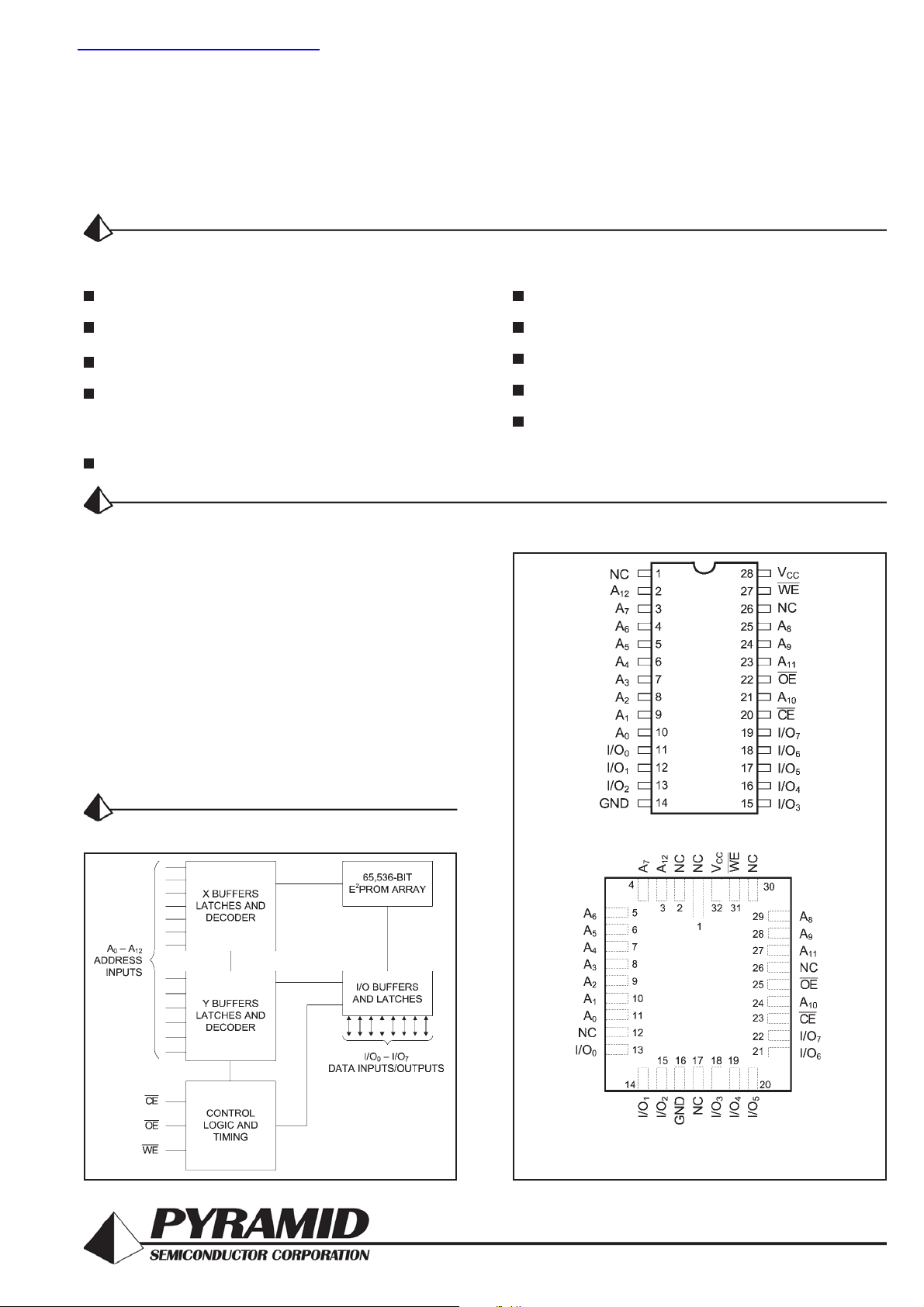
FUNCTIONAL BLOCK DIAGRAM
PIN CONFIGURATIONS
1519B
DIP (C5-1)
LCC (L6)
Software Data Protection
Fully TTL Compatible Inputs and Outputs
Endurance: 10,000 or 100,000 Cycles
Data Retention: 100 Years
Available in the following Packages:
– 32-Pin Ceramic LCC (450 x 550 mils)
– 28-Pin 600 mil Ceramic DIP
查询PYX28C64-20L32M供应商

PYX28C64
Page 2 of 11Document # EEPROM101 REV B
MAXIMUM RATINGS
(1)
Symbol Parameter Value Unit
V
CC
Power Supply Pin with –0.3 to +6.25 V
Respect to GND
Terminal Voltage with –0.5 to
V
TERM
Respect to GND +6.25 V
(up to 6.25V)
T
A
Operating Temperature –55 to +125 ° C
Symbol Parameter Value Unit
T
BIAS
Temperature Under –55 to +125 ° C
Bias
T
STG
Storage Temperature –65 to +150 ° C
P
T
Power Dissipation 1. 0 W
I
OUT
DC Output Current 50 mA
RECOMMENDED OPERATING
TEMPERATURE AND SUPPLY VOLTAGE
I
SB
Standby Power Supply
Current (TTL Input Levels)
CE ≥ VIH, OE = VIL,
VCC= Max,
f = Max., Outputs Open
___ 3
250
mA
µA___
CE ≥ VHC,
VCC= Max,
f = 0, Outputs Open
VIN ≤ VLC or VIN ≥ V
HC
Standby Power Supply
Current
(CMOS Input Levels)
I
SB1
Grade
(2)
Ambient
Temperature
GND
V
CC
0V
5.0V ± 10%
–55°C to +125°C
Military
Symbol
C
IN
C
OUT
Parameter
Input Capacitance
Output Capacitance
Conditions
VIN = 0V
V
OUT
= 0V
10
10
Unit
pF
pF
CAPACITANCES
(4)
VCC = 5.0V, TA = 25°C, f = 1.0MHz
Symbol
DC ELECTRICAL CHARACTERISTICS
Over recommended operating temperature and supply voltage
(2)
V
IH
V
IL
V
HC
V
LC
V
OL
V
OH
I
LI
I
LO
Parameter
Input High Voltage
Input Low Voltage
CMOS Input High Voltage
CMOS Input Low Voltage
Output Low Voltage
(TTL Load)
Output High Voltage
(TTL Load)
Input Leakage Current
Output Leakage Current
Test Conditions
IOL = +8 mA, VCC = Min.
IOH = –4 mA, VCC = Min.
VCC = Max.
VIN = GND to V
CC
VCC = Max., CE = VIH,
V
OUT
= GND to V
CC
P5C164
Min
2.0
–0.5
(3)
VCC –0.2
–0.5
(3)
2.4
–10
–10
VCC +0.3
0.8
VCC +0.5
0.2
0.4
+10
+10
Max
Unit
V
V
V
V
V
V
µA
µA
Notes:
1. Stresses greater than those listed under MAXIMUM RATINGS may
cause permanent damage to the device. This is a stress rating only
and functional operation of the device at these or any other conditions
above those indicated in the operational sections of this specification
is not implied. Exposure to MAXIMUM rating conditions for extended
periods may affect reliability.
2. Extended temperature operation guaranteed with 400 linear feet per
minute of air flow.
3. Transient inputs with VIL and IIL not more negative than –3.0V and
–100mA, respectively, are permissible for pulse widths up to 20 ns.
4. This parameter is sampled and not 100% tested.
Typ.
60 mA___
CE = OE = VIL,
WE = VIH,
All I/O's = Open,
Inputs = VCC = 5.5V
Supply Current
I
CC

PYX28C64
Page 3 of 11Document # EEPROM101 REV B
AC ELECTRICAL CHARACTERISTICS—READ CYCLE
(VCC = 5V ± 10%, All Temperature Ranges)
(2)
Min Max Min Max Min Max Min Max
t
AVAV
Read Cycl e Time 200 250 300 350 n s
t
AVQV
Address Acces s Time 200 250 300 350 ns
t
ELQV
Chip Enable Access T ime 200 250 300 350 ns
t
OLQV
Outpu t Enabl e Access Time 100 100 100 100 ns
t
ELQX
Chip Enable to Output in Low Z10101010ns
t
EHQZ
Chip Disable to Output in High Z 80808080ns
t
OLQX
Output Enable to Output in Low Z 10 10 10 10 ns
t
OHQZ
Outpu t Disable to Output in High Z 80 80 80 80 ns
t
AVQX
Output Hold from Address Change0000ns
t
PU
Chip Enable t o Power U p T ime 250 250 250 250 ns
t
PD
Chip Disabl e t o Pow er Down T im e 50 50 50 50 ns
-300 -350
UnitSymbol Parameter
-200 -250
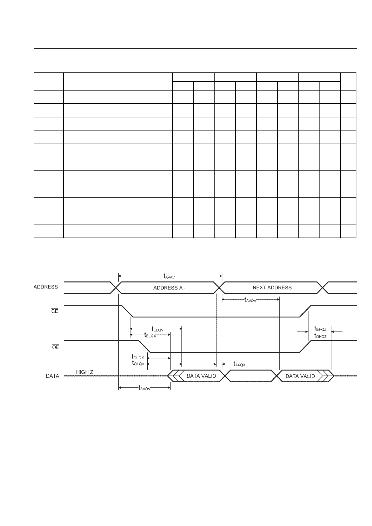
TIMING WAVEFORM OF READ CYCLE

PYX28C64
Page 4 of 11Document # EEPROM101 REV B
AC CHARACTERISTICS—WRITE CYCLE
(VCC = 5V ± 10%, All Temperature Ranges)
(2)
Min Max Min Max Min Max Min Max
t
WHWL1
t
EHEL1
Writ e Cycl e Time 10 10 10 10 ms
t
AVEL
t
AVWL
Address Setup Time 20 20 20 20 ns
t
ELAX
t
WLAX
Address Hold Time 150 150 150 150 ns
t
WLEL
t
ELWL
Write Setup Time 0000ns
t
WHEH
Write Hold Time 0000ns
t
OHE L
t
OHWL
OE
Setup Time 20 20 20 20 ns
t
WHOL
OE
Hol d Time 20 20 20 20 ns
t
ELEH
t
WLWH
WE
Pulse Width 150 150 150 150 ns
t
DVEH
t
DVWH
Data Setup T im e 50 50 50 50 ns
t
EHDX
t
WHDX
Data Hold T ime 10 10 10 10 ns
t
EHEL2
t
WHWL2
Byte Load Cy cl e T im e 0.2 2 0. 2 2 0.2 2 0.2 2 µs
t
ELWL
CE
Setup Time 1111µs
t
OVHWL
Output Setup Time 1111µs
t
EHWH
CE
Hold Time 1111µs
t
WHOH
OE
Hold Time 1111µs
t
OHAV
Erase Time 200 200 200 200 ms
t
WLWH2
Chip Erase Time 150 150 150 150 ns
V
H
High Voltage for Chip Clear 1213121312131213V
-300 -350
UnitSymbol Parameter
-200 -250
 Loading...