PYRAMID PY264 Technical data

1
Document # EPROM102 REV OR
Revised July 2007
PY264
8K X 8 REPROGRAMMABLE PROM
DESCRIPTION
The PY264 is an 8Kx8 CMOS PROM. The device is
available in windowed packages which when exposed to
UV light, the memory content in the PROM is erased and
can be reprogrammed. EPROM technology is used in
the memory cells for programming. The EPROM requires a 12.5V for programming. Devices are tested to
insure that performance of the device meets the DC and
AC specification limits after customer programming.
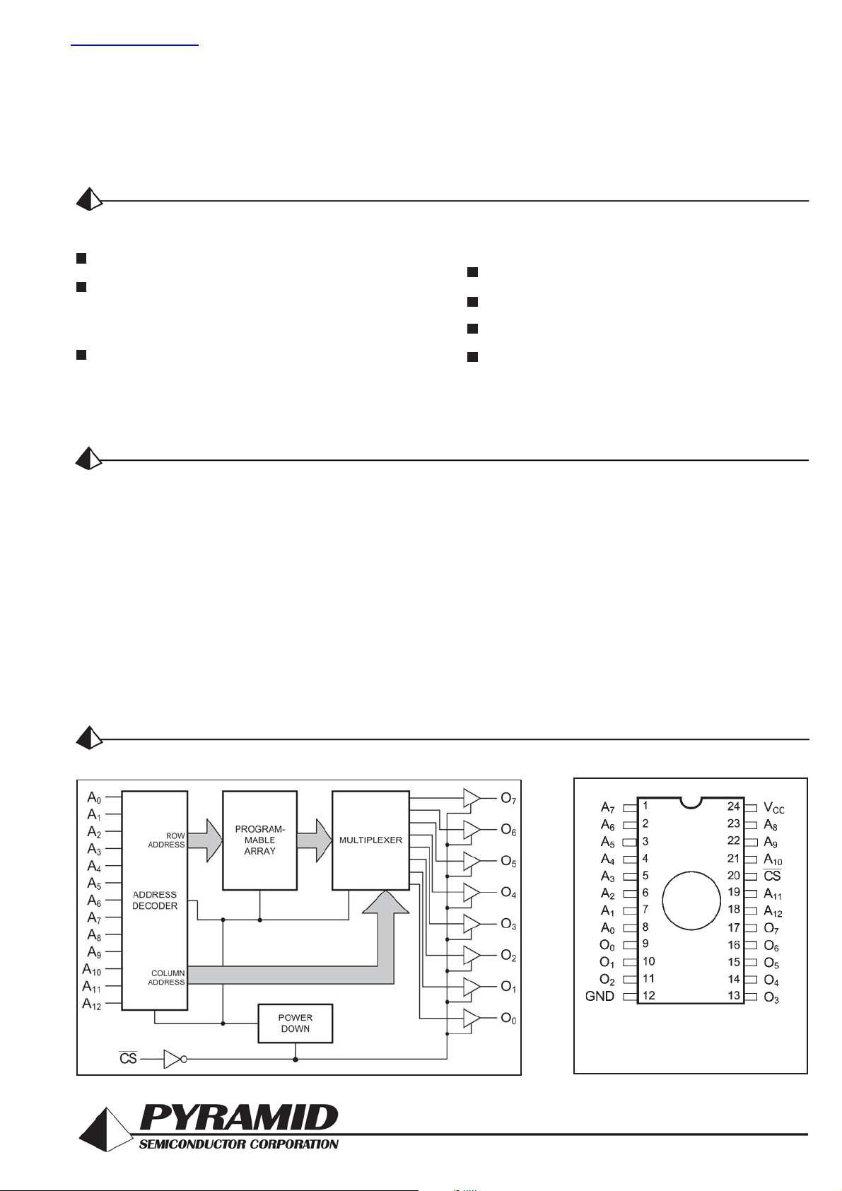
To perform a read operation from the device, CS is LOW.
The memory contents in the address established by the
Address pins (A0 to A12) will become available on the
outputs (O0 to O7).
The PY264 is available in 24-pin 600 mil Ceramic DIPs
(Windowed) and Plastic DIPs (Non-Windowed).
FUNCTIONAL BLOCK DIAGRAM
PIN CONFIGURATION
FEATURES
EPROM Technology for reprogramming
High Speed
– 35/45/55 ns (Commercial)
– 35/45/55 ns (Military)
Low Power Operation:
– 660 mW Commercial
– 770 mW Military
Single 5V±10% Power Supply
Windowed devices for reprogramming
Fully TTL Compatible Inputs and Outputs
Standard Pinout (JEDEC Approved):
– 24-Pin 600 mil Windowed CERDIP
– 24-Pin 600 mil Non-Windowed Plastic DIP
DIP (P8, WD2)
Note: Window on
WD2 package only
查询PY264供应商

PY264
Page 2 of 8Document # EPROM102 REV OR
MAXIMUM RATINGS
(1)
Symbol Parameter Value Unit
V
CC
Power Supply Pin with –0.5 to +7 V
Respect to GND
Terminal Voltage with –0.5 to
V
TERM
Respect to GND VCC +0.5 V
(up to 7.0V)
V
PP
Program Voltage 13 V
Symbol Parameter Value Unit
T
A
Operating Temperature –55 to +125 °C
T
BIAS
Temperature Under –55 to +125 °C
Bias
T
STG
Storage Temperature –65 to +150 °C
P
T
Power Dissipation 1.0 W
I
OUT
DC Output Current 50 mA
Symbol Parameter Conditions Typ. Unit
C
IN
Input Capacitance VIN = 0V 10 pF
C
OUT
Output Capacitance V
OUT
= 0V 10 pF
Grade
(2)
Ambient Temp Gnd Vcc
Commercial 0°C to 70°C 0V 5.0V ±10%
Military -55°C to +125°C 0V 5.0V ±10%
RECOMMENDED OPERATING CONDITIONS
CAPACITANCES
(4)
(VCC = 5.0V, TA = 25°C, f = 1.0MHz)
DC ELECTRICAL CHARACTERISTICS
Over recommended operating temperature and supply voltage
(2)
V
PP
Programming Supply Voltage 12 13
50
V
mA
Programming Supply Current I
PP
Symbol
V
IH
V
IL
V
HC
V
LC
V
OL
V
OH
I
LI
I
LO
Parameter
Input High Voltage
Input Low Voltage
CMOS Input High Voltage
CMOS Input Low Voltage
Output Low Voltage (TTL Load)
Output High Voltage (TTL Load)
Input Leakage Current
Output Leakage Current
Test Conditions
IOL = +16 mA, VCC = Min.
IOH = –4 mA, VCC = Min.
VCC = Max.
VIN = GND to V
CC
VCC = Max., CE = VIH,
V
OUT
= GND to V
CC
PY264
Min
2.0
–0.5
(3)
VCC –0.2
–0.5
(3)
2.4
–10
–10
Max
V
CC
0.8
VCC +0.5
0.2
0.4
+10
+10
Unit
V
V
V
V
V
V
µA
µA
I
CC
Symbol Parameter Temperature Range
Dynamic Operating Current*
Commercial
Military
–35 –55 Unit
mA
mA
POWER DISSIPATION CHARACTERISTICS VS. SPEED
120 120 120
100 100 100
–45
V
IHP
Input HIGH Programming Voltage 4.75
V
V
ILP
Input LOW Programming Voltage
0.4 V
COM
–40 +40
µA
MIL

PY264
Page 3 of 8Document # EPROM102 REV OR
AC ELECTRICAL CHARACTERISTICS—READ CYCLE
(VCC = 5V ± 10%, All Temperature Ranges)
(2)
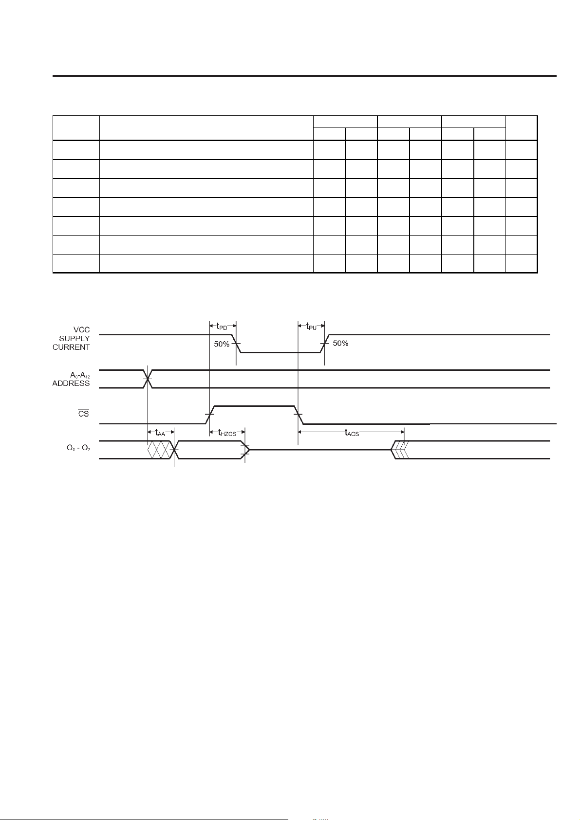
TIMING WAVEFORM OF READ CYCLE
Notes:
1. Stresses greater than those listed under MAXIMUM RATINGS may
cause permanent damage to the device. This is a stress rating only
and functional operation of the device at these or any other conditions
above those indicated in the operational sections of this specification
is not implied. Exposure to MAXIMUM rating conditions for extended
periods may affect reliability.
2. Extended temperature operation guaranteed with 400 linear feet per
minute of air flow.
3. Transient inputs with VIL and IIL not more negative than –3.0V and
–100mA, respectively, are permissible for pulse widths up to 20 ns.
4. This parameter is sampled and not 100% tested.
Min Max Min Max Min Max
t
AA
Addres s to Output V ali d 35 45 55 ns
t
HZCS1
Chip Select Inactive to High Z 20 30 35 ns
t
ACS1
Chip Select Active to Output Valid 20 30 35 ns
t
HZCS2
Chip Select Inactive to High Z 35 45 55 ns
t
ACS2
Chip Select Active to Output Valid 35 45 55 ns
t
PU
Chip Select Active to Power-Up 0 0 0 ns
t
PD
Chip Slec t Inactive to Power-Down 35 45 55 ns
UnitSymbol Parame ter
-45-35 -55
 Loading...