PYRAMID P4C167, P4C167L Technical data

查询P4C167L-10CMB供应商
P4C167/P4C167L
ULTRA HIGH SPEED 16K X 1
STATIC CMOS RAMS
FEATURES
Full CMOS, 6T Cell
High Speed (Equal Access and Cycle Times)
– 10/12/15/20/25 ns (Commercial)
– 12/15/20/25/35 ns (Industrial)
– 15/20/25/35/45 ns (Military)
Low Power Operation
Single 5V±10% Power Supply
Data Retention with 2.0V Supply (P4C167L
Military)
DESCRIPTION
The P4C167/L are 16,384-bit high speed static RAMs organized as 16K x 1. The CMOS memories require no clocks
or refreshing and have equal access and cycle times. The
RAMs operate from a single 5V ± 10% tolerance power
supply. Data integrity is maintained for supply voltages
down to 2.0V, typically drawing 10µA.
Separate Data I/O
Three-State Output
TTL Compatible Output
Fully TTL Compatible Inputs
Standard Pinout (JEDEC Approved)
– 20-Pin 300 mil DIP
– 20-Pin 300 mil SOJ
– 20-Pin LCC
Access times as fast as 10 nanoseconds are available,
greatly enhancing system speeds. CMOS reduces power
consumption to low levels.
The P4C167/L are available in 20-pin 300 mil DIP, 20-pin
300 mil SOJ, and 20-pin LCC packages providing excellent board level densities.
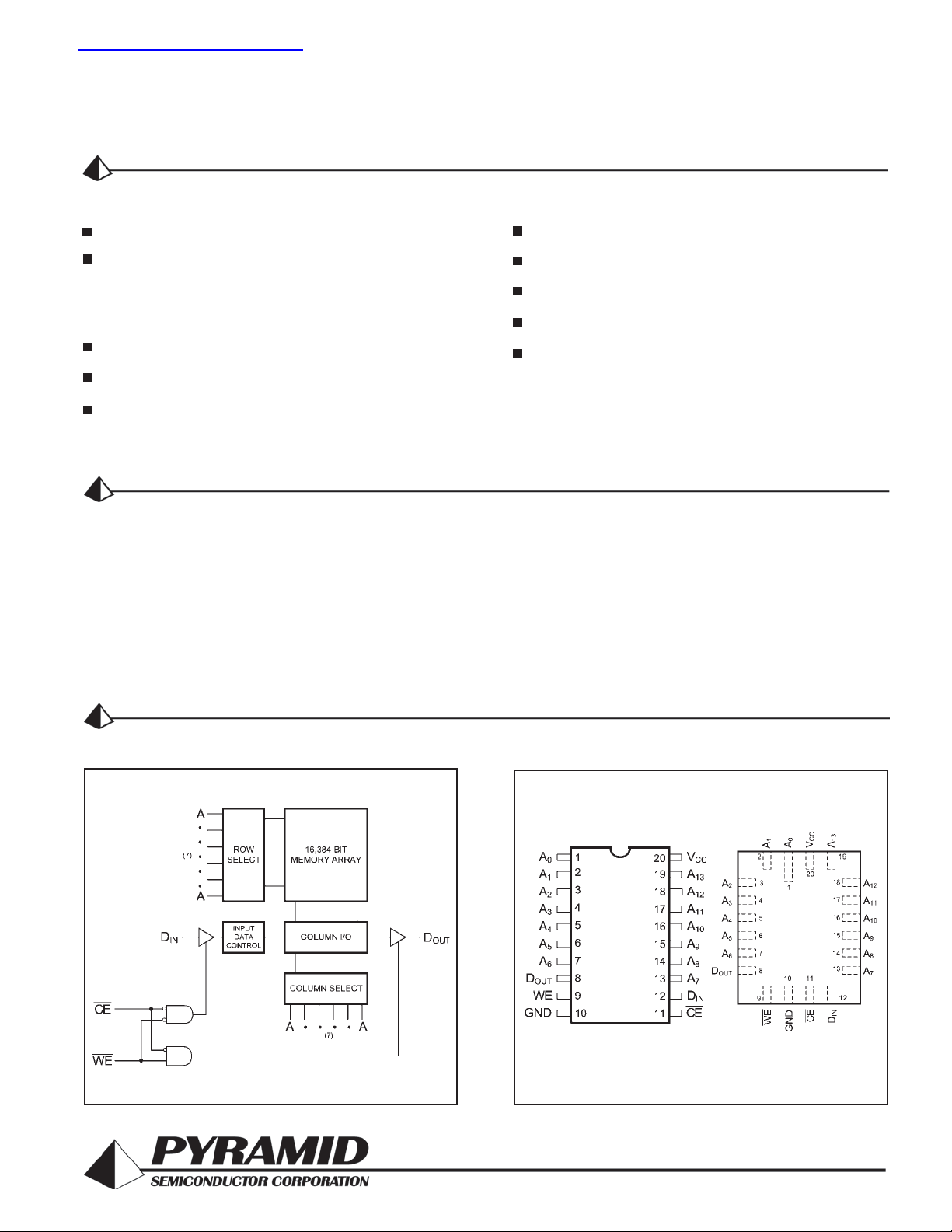
PIN CONFIGURATIONSFUNCTIONAL BLOCK DIAGRAM
DIP (P2, C6)
SOJ (J2) SIMILAR
Document # SRAM106 REV A
1
1
LCC (L9)
Revised October 2005

P4C167
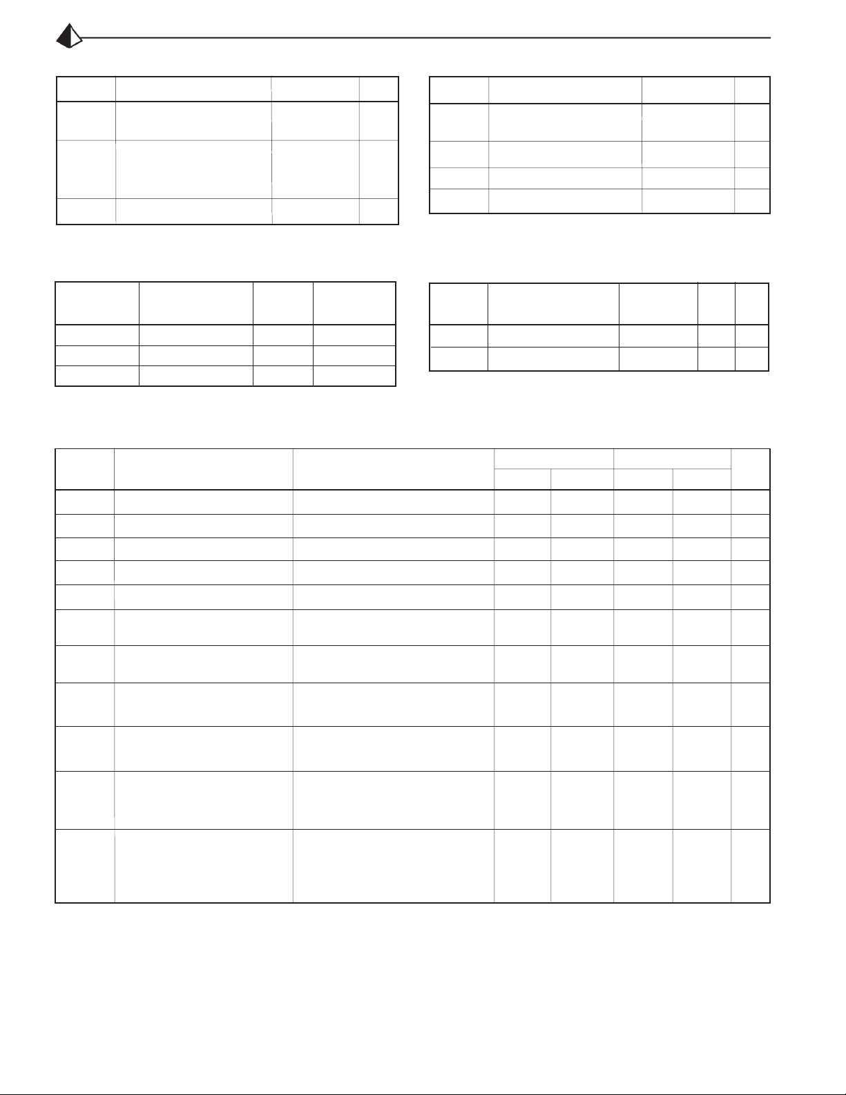
MAXIMUM RATINGS
(1)
Symbol Parameter Value Unit
V
CC
Power Supply Pin with –0.5 to +7 V
Respect to GND
Terminal Voltage with –0.5 to
V
TERM
Respect to GND VCC +0.5 V
(up to 7.0V)
T
A
Operating Temperature –55 to +125 °C
RECOMMENDED OPERATING
TEMPERATURE AND SUPPLY VOLTAGE
Grade(2)
Military
Industrial
Commercial
Ambient
Temperature
–55°C to +125°C
–40°C to +85°C
0°C to +70°C
GND
0V
0V
0V
V
CC
5.0V ± 10%
5.0V ± 10%
5.0V ± 10%
DC ELECTRICAL CHARACTERISTICS
Over recommended operating temperature and supply voltage
Symbol Parameter Value Unit
T
BIAS
Temperature Under –55 to +125 °C
Bias
T
STG
P
T
I
OUT
CAPACITANCES
Storage Temperature –65 to +150 °C
Power Dissipation 1.0 W
DC Output Current 50 mA
(4)
VCC = 5.0V, TA = 25°C, f = 1.0MHz
Symbol
C
IN
C
OUT
(2)
Parameter
Input Capacitance
Output Capacitance
Conditions
VIN = 0V
V
= 0V
OUT
Typ.
5
7
Unit
pF
pF
Symbol
V
V
V
V
V
V
V
I
I
Input High Voltage
IH
Input Low Voltage
IL
CMOS Input High Voltage
HC
CMOS Input Low Voltage
LC
Input Clamp Diode Voltage
CD
Output Low Voltage
OL
(TTL Load)
Output High Voltage
OH
(TTL Load)
I
Input Leakage Current
LI
Output Leakage Current
LO
Standby Power Supply
SB
Current (TTL Input Levels)
Standby Power Supply
I
SB1
Current
(CMOS Input Levels)
n/a = Not Applicable
Parameter
Test Conditions
VCC = Min., IIN = –18 mA
IOL = +8 mA, VCC = Min.
IOH = –4 mA, VCC = Min.
VCC = Max. Mil.
VIN = GND to VCC Com’l.
VCC = Max., CE = VIH, Mil.
V
= GND to VCC Com’l.
OUT
CE ≥ V
V
Mil.
IH
= Max ., Ind./Com’l.
CC
f = Max., Outputs Open
CE ≥ V
V
CC
Mil.
HC
= Max., Ind./Com’l.
f = 0, Outputs Open
V
≤ V
or V
IN
LC
IN
≥ V
HC
P4C167
Min
2.2
(3)
–0.5
VCC –0.2
(3)
–0.5
2.4
–10
–5
–10
–5
___
___
___
___
Max
VCC +0.5
0.8
VCC +0.5
0.2
–1.2
0.4
+10
+5
+10
+5
30
20
15
10
P4C167L
Min Max
2.2
(3)
–0.5
VCC –0.2
–0.5(3)
2.4
–5
n/a
–5
n/a
___
___
___
___
VCC +0.5
0.8
VCC +0.5
0.2
–1.2
0.4
+5
n/a
+5
n/a
20
n/a
1.0
n/a
Unit
V
V
V
V
V
V
V
µA
µA
mA
mA
Notes:
1. Stresses greater than those listed under MAXIMUM RATINGS may
cause permanent damage to the device. This is a stress rating only
and functional operation of the device at these or any other conditions
above those indicated in the operational sections of this specification
is not implied. Exposure to MAXIMUM rating conditions for extended
periods may affect reliability.
2. Extended temperature operation guaranteed with 400 linear feet per
minute of air flow.
3. Transient inputs with VIL and IIL not more negative than –3.0V and
–100mA, respectively, are permissible for pulse widths up to 20 ns.
4. This parameter is sampled and not 100% tested.
Page 2 of 10Document # SRAM106 REV A

POWER DISSIPATION CHARACTERISTICS VS. SPEED
P4C167
Symbol Parameter
Dynamic Operating Current*
I
CC
*VCC = 5.5V. Tested with outputs open. f = Max. Switching inputs are 0V and 3V. CE = VIL.
Temperature
Range
Commercial
Industrial
Military
–10
–12 –15 –20 –25 –35 –45
180 170 160 155 150 N/A N/A
N/A 150155160170180
N/A
N/A 170 160 155 150 145
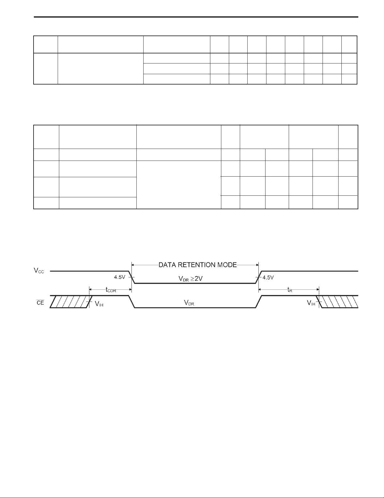
DATA RETENTION CHARACTERISTICS (P4C167L Military Temperature Only)
Typ.*
Symbol
V
I
CCDR
t
CDR
DR
VCC for Data Retention
Data Retention Current
Chip Deselect to
Data Retention Time
†
t
R
*TA = +25¹C
§tRC = Read Cycle Time
†
This parameter is guaranteed but not tested.
Operation Recovery Time
Parameter
Test Conditons
CE ≥ V
V
or V
IN
≥ V
–0.2V,
CC
–0.2V
CC
≤ 0.2V
IN
Min
2.0
0
t
RC
2.0V 3.0V
10
§
VCC =
2.0V 3.0V
15 600 900
Max
VCC =
Unit
N/AmAmA
mA
Unit
V
µA
ns
ns
DATA RETENTION WAVEFORM
Page 3 of 10Document # SRAM106 REV A
 Loading...