

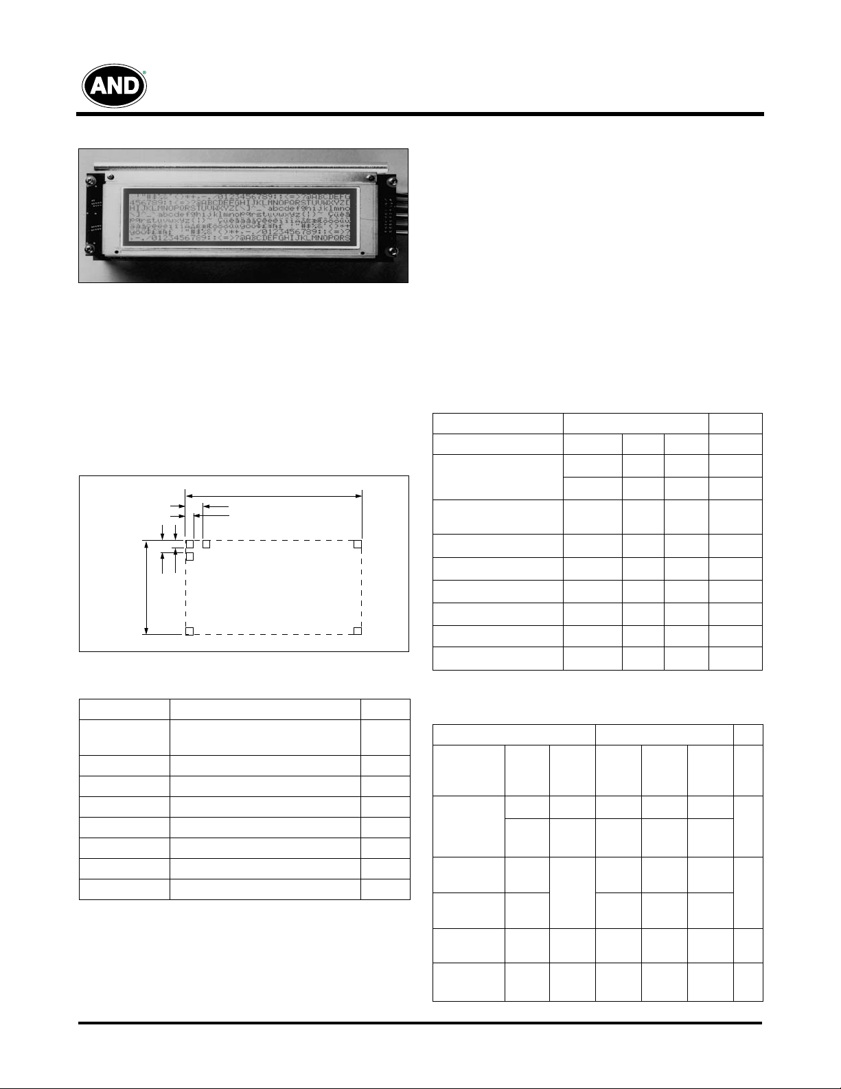
AND1781MST/BST
240 x 64 Dots
Intelligent Graphics Display
The AND1781MST/BST devices are compact, full dot matrix,
with “white page” appearance, LCD modules that have an onboard LCD controller (T6963C) and display memory (RAM).
Features
• RoHS Compliant
• Black and white ST (MST) transmissive mode
• Blue and white (BST) transmissive mode
• Built-in CCFL backlight
• 40 characters x 8 line capability
• 240 x 64 dot graphic display
• Excellent readability and high-contrast ratio
• Built-in LCD controller (T6963C)
• Wide operating temperature range (0° to 50°C)
• User-selectable fonts: 6 x 8 or 8 x 8
Dot Matrix Dimensions
127.17
0.53
0.50
33.89
0.59
0.50
240 x 64 pixels
Mechanical Characteristics
Item Specification Unit
Outline
Dimensions
180.0 (W) x 70.0 (H) x 14.0 Max (D) mm
Number of Dots 240 x 64 Dots
# of Characters 40 x 8 (480), 6 x 8 font
Viewing Area 127.17 (W) x 33.89 (H) mm
Bezel Opening 137.0 (W) 44.0 (H) mm
Dot Size 0.50 (W) 0.50 (H) mm
Dot Pitch 0.53 (W) 0.53 (H) mm
Weight (approx.) 170 gram
Product specifications contained herein may be changed
without prior notice. It is therefore advisable to contact
Purdy Electronics before proceeding with the design of
equipment incorporating this product.
The AND1781 can display TEXT information, numerals,
letters and symbols, as well as GRAPHIC patterns. These
devices are suitable for medical and measurement
equipment, point-of-sale terminals, portable equipment, and
marine instrumentation.
Absolute Maximum Ratings
Absolute Maximum
Item Symbol Min Max Unit
V
Supply Voltage
CCFL Input Current
CCFL Driving Voltage
(1)
CCFL Drive Frequency
Input Voltage
Storage Temperature
Operating Temperature
(2)
Humidity
1. 1 minute maximum.
2. Wet bulb temperature ≤ 29° C, no condensation of water.
DD
V
- V
DD
I
FL
V
FL
f
FL
V
IN
T
stg
T
OP
– 10 90 °/° RH
0 7.0 V
0 28.0 V
EE
–10
– 1500
– 35 kHz
-0.03 0.3 V
-20 60 °C
050 °C
mA
rms
V
rms
Electrical Characteristics (TA = 25°C)
Specifications
Item Symbol Cond.
V
Supply
Voltage
High Level In
V
Low Level
In V
FL Driving V
FL Input
(1)
Current
DD
V
-
DD
V
EE
V
IN
V
IH
V
IN
I
FL
V
DD
5.0V
V
FL
Min.
(BST/
MST)
4.75 5.0 5.25
11.2/
12.0
2.8 —
=
4.0 5.0 7.0
Typ.
(BST/
MST)
12.2/
13.0
Max.
(BST/
MST)
13.2/
14.0
V
DD
0 — 0.8
— 300 350
Unit
V
V
V
rms
mA
rms
7/20/07
Tel: 408.523.8200 • Fax: 408.733.1287 • email@purdyelectronics.com • www.purdyelectronics.com
Purdy Electronics Corporation • 720 Palomar Avenue • Sunnyvale, CA 94085
1
E1241/42
CCF
Tube
1
2
3
4
V
out
+
-
Input bypass capacitor may be required (10µf –47µf)
AND1781MST/BST
Intelligent Graphics Display
Electrical Characteristics (TA = 25°C) (Continued)
Item Symbol Cond.
FL Starting V
FL Driving Fre-
V
Ta = 0°C 1300 — —
FLS
IFL(2)
quency
I
DD
Typical
Pattern
I
I
I
EE
DD
EE
Max.
Pattern
Current
Consumption
1. Life time of backlight will change according to the FL input
current.
2. Choose a driving frequency that is not in sync with the frame
frequency otherwise, you may experience flickering.
3. Typical pattern is all “on”, maximum pattern is checkered.
Optical Characteristics (TA = 25˚C, φ = 0°, θ = 0)
Item Symbol
Viewing Angle
Right to Left – 80
Up & Down – 55
Contrast Ratio K 2.5/8 3.5/20 — —
T
Response Time
Luminance
I
= 5.0 mA rms
FL
ON
T
OFF
L5080—
Note: Refer to Applications Section for definitions of viewing
angle, contrast ratio, response time (“on” and “off”)
and luminance.
Connector Pin Assignment
Pin No. Signal Function
1 FGND Frame Ground
2 GND Ground
3
4
V
V
5WR
6RD
7CE
Power Supply (5V)
DD
Power Supply for LCD Drive
EE
Data Write
Data Read
Chip Enable
WR = “L”, C/D = “H”: Command Write
WR
8 C/D
2
9 NC No connection
Tel: 408.523.8200 • Fax: 408.733.1287 • email@purdyelectronics.com • www.purdyelectronics.com
= “L”, C/D = “L”: Data Write
RD
= “L”, C/D = “H”: Status Read
RD
= “L”, C/D = “L”: Data Read
Purdy Electronics Corporation • 720 Palomar Avenue • Sunnyvale, CA 94085
Specifications
Min.
(BST/
MST)
Typ.
(BST/
MST)
25 30 35 kHz
— 7.0 14.0
(3)
— 1.0 2.0
— 8.0 16.0
(3)
— 1.5 3.0
Specifications
Min.
(BST/
MST)
Typ.
(BST/
MST)
Max.
(BST/
MST)
— 200 350
— 200 350
Max.
(BST/
MST)
Unit
V
O-P
mA
Unit
degree
ms
cd/m
Connector Pin Assignment (Continued)
Pin No. Signal Function
10 RESET
Controller Reset
11 D0 Data Input/Output (LSB)
12 D1 Data Input/Output
13 D2 Data Input/Output
14 D3 Data Input/Output
15 D4 Data Input/Output
16 D5 Data Input/Output
17 D6 Data Input/Output
18 D7 Data Input/Output (MSB)
19 FS
20 RV
Connect to V
Connect to GND: 8 x 8 font
V
: Positive image
DD
GND: Negative image
: 6 x 8 font
DD
FL Connector
Pin No, Signal Function
1
5
V
Power supply for FL backlight
FL
V
Power supply for FL backlight
FL
Note: Connector: IL-G-55-53C2, Japan Aviation Electronics
Industry. Mating Housing: IL-M-5P-S3C2-PM.
Contact: IL-M-C2.
Recommended FL Inverter
2
Part number E1241/42 (part number E1241 is +5v, number
E1242 is +12V). This part is manufactured by Endicott
Research Group, Inc.. Method of connecting is illustrated.
Power Supply
LCD panel is driven by the voltage V
V
is required for contrast control and temperature
EE
compensation.
Temperature Variations
V
Temperature
DD
–V
EE
0°C 13.5 14.3
+25°C 12.2 13.0
+50°C 11.0 11.8
–V
DD
(MST) V
, so adjustable
EE
–V
(BST)
DD
EE
7/20/07

t
CDS
tCP,tRD,t
WP
t
ACC
t
CDH
t
DH
t
OH
t
DS
C/D
CE
RD, WR
D0-D7
(WRITE)
D0-D7
(READ)
AND1781MST/BST
Intelligent Graphics Display
Timing Relationships and Diagram
Signal Timing Relationships
Item Symbol Min. Max. Unit
C/D Set Up Time
C/D Hold Time
CE
RD
WR
,
,
Pulse Width
Data Set Up Time
Data Hold Time
Access Time
Output Hold Time
Block Diagram
t
t
t
, t
CE
t
D0–D7
WR
RD
C/
RESET
CDS
CDH
RD
t
DS
t
DH
ACC
t
OH
RV
CE
D
FS
100 –
10 –
, t
WR
80 –
80 –
40 –
– 150
10 50
T6963C
8
13
R/W
CE
ED
HSC
LP
CDAT
ns
D0–D7
RAM
(8K byte)
A0–A7
Timing Diagram
Revers
e
80 80 80
X-Driver X-DriverX-Driver
Dimensional Outline
14.5±0.5
70.0±0.5
50.0±0.3
7/20/07
Tel: 408.523.8200 • Fax: 408.733.1287 • email@purdyelectronics.com • www.purdyelectronics.com
64
Y-Driver
V
FL
V
FL
5.0±0.5
8.0±0.5
10.06±0.5
Reference Line
33.89
44.0±0.3
38.0±0.3
24.42±0.5
22.5±0.5
19.5±0.5
8.6±0.5
2.0±0.5
Purdy Electronics Corporation • 720 Palomar Avenue • Sunnyvale, CA 94085
127.17 (Active Area)
131.0±0.3 (Viewing Area)
137.0±0.3 (Bezel Opening)
158.8±0.5
176.0±0.3
180.0±0.5
LCD Panel
240 x 64 Dots
FL Backlight
2.54±0.3
2201
22.86±0.3 13.0±0.5
20-ø1.0 (Through Hole)
20-ø1.6 (Land)
4-R1.75
2.54±0.3
2.54±0.3
Reserve
Line
7.5±0.5
14.0 Max
CN
130±10
1.6±0.3
3
 Loading...