

Page 1

TCF–10B
FREQUENCY-PROGRAMMABLE
FREQUENCY-SHIFT CARRIER
TRANSMITTER/RECEIVER
System Manual
CF44—VER05
(Replaces CF44—VER04)
Technologies, Inc.
4050 NW 121st Avenue
Coral Springs, FL USA 33065
1–800–785–7274
www.pulsartech.com
Printed December 2004
Page 2

Technologies, Inc.
Page 3

1
Product Description
2
Applications and Ordering Information
3
Installation
4
Test Equipment
5
Installation/Adjustment Procedures
6
Signal Path
7
Design Verification Tests
8
Maintenance
9
Power Supply Module
10
Keying Module
11
Transmitter Module
12
10W PA Module
13
RF Interface Module
14
Universal Receiver Module
15
Receiver Logic Module
16
Optional EM Output Module
17
Optional Voice Adapter Module
18
Optional Trip Test Unit Module
TCF–10B
System Manual
Table
of
Contents
Page 4

ii December 2004
Te chnologies, Inc.
Important Change Notification
This document supersedes the TCF–10B Frequency-Programmable Frequency-Shift Carrier
Transmitter/Receiver System Manual CF44–VER04. The following list shows the most recent publication
date for each chapter. Publication dates in bold type indicate changes to that chapter since the previous
publication. For these chapters, the specific pages that have changed are listed for easy reference. Note that
only significant changes, i.e., those changes which affect the technical use and understanding of the
document and the TCF–10B equipment, are reported. Changes in format, typographical corrections, minor
word changes, etc. are not reported. Note also that in some cases text and graphics may have flowed to a
different page than in the previous publication due to formatting or other changes. The page numbers
below show the current pages on which the reported changes appear.
Each reported change is identified in the document by a change bar, || placed to its immediate left and/or
right, just like the ones on this page.
Chapter Number & Title Publication Date Pages with Changes
|| Front Section December 2004 ii, v
|| 1. Product Description December 2004 1, 8
|| 2. Applications and Ordering Information December 2004 11, 16
|| 3. Installation December 2004 5
4. Test Equipment April 1997
|| 5. Installation/Adjustment Procedures December 2004 5, 12, 13
|| 6. Signal Path December 2004 5 (11x17)
|| 7. Design Verification Tests December 2004 5
8. Maintenance October 2001
|| 9. Power Supply Module December 2004 1, 4, 5
||10. Keying Module December 2004 1
||11.Transmitter Module December 2004 1, 2, 3, 4
||12. 10W PA Module December 2004 1, 4
||13. RF Interface Module December 2004 1
14. Universal Receiver Module October 2001
||15. Receiver Logic Module December 2004 1, 3, 4, 7, 10, 13
||16. EM Output Module December 2004 1
||17. Optional Voice Adapter Module December 2004 1
||18. Optional Trip Test Unit December 2004 3, 9
Note: due to design changes, nomenclature throughout this document indicating 300, 600 & 1200 Hz has been changed to 380,
800 & 1600 Hz respectively.
Page 5

December 2004 iii
TCF–10B System Manual
e recommend that you become acquainted with the information in this manual before energizing your TCF–10B system. Failure to do so may result in injury to personnel or damage to
the equipment, and may affect the equipment warranty. If you mount the carrier set in a cabinet,
it must be bolted to the floor or otherwise secured before you swing out the equipment, to
prevent the installation from tipping over.
You should not remove or insert printed circuit modules while the TCF–10B is energized.
Failure to observe this precaution can result in undesired tripping output and can cause
component damage.
PULSAR does not assume liability arising out of the application or use of any product or circuit
described herein. PULSAR reserves the right to make changes to any products herein to improve
reliability, function or design. Specifications and information herein are subject to change
without notice. All possible contingencies which may arise during installation, operation, or
maintenance, and all details and variations of this equipment do not purport to be covered by
these instructions. If you desire further information regarding a particular installation,
operation, or maintenance of equipment, please contact your local Pulsar Technologies, Inc.
representative.
Copyright ©
By Pulsar Technologies, Inc.
ALL RIGHTS RESERVED
PULSAR does not convey any license under its patent rights nor the rights of others.
!
W
ESD Warning!
YOU MUST BE PROPERLY GROUNDED, TO PREVENT DAMAGE FROM
STATIC ELECTRICITY, BEFORE HANDLING ANY AND ALL MODULES OR
EQUIPMENT FROM PULSAR.
All semiconductor components used, are sensitive to and can be damaged by the
discharge of static electricity. Be sure to observe all Electrostatic Discharge (ESD)
precautions when handling modules or individual components.
IMPORTANT
Page 6

Preface
Scope
This manual describes the functions and features of the TCF–10B Power Line Carrier Transmitter/
Receiver. It is intended primarily for use by engineers and technicians involved in the installation,
alignment, operation, and maintenance of the TCF–10B.
Equipment Identification
The TCF–10B equipment is identified by the Catalog Number on the TCF–10B chassis nameplate. You
can decode the Catalog Number using the information in Chapter 2.
Production Changes
When engineering and production changes are made to the TCF–10B equipment, a revision notation (Sub
number) is reflected in the style number and related schematic diagrams. A summary of all Sub numbers
for the particular release is shown on the following page.
Warranty
Our standard warranty extends for 60 months after shipment. For all repaired modules or advance replacements, the standard warranty is 90 days or the remaining warranty time, whichever is longer. Damage
clearly caused by improper application, repair, or handling of the equipment will void the warranty.
Equipment Return & Repair Procedure
To return equipment for repair or replacement:
1. Call your PULSAR representative at 1–800–785–7274.
2. Request an RMA number for proper authorization and credit.
3. Carefully pack the equipment you are returning.
Repair work is done most satisfactorily at the factory. When returning any equipment, pack it in
the original shipping containers if possible. Be sure to use anti-static material
when packing the
equipment. Any damage due to improperly packed items will be charged to the customer, even
when under warranty.
Pulsar Technologies, Inc. also makes available interchangeable parts to customers who are
equipped to do repair work. When ordering parts (components, modules, etc.), always give the
complete PULSAR style number(s).
4. Make sure you include your return address and the RMA number on the package.
5. Ship the package(s) to:
Pulsar Technologies, Inc.
Communications Division
4050 NW 121st Avenue
Coral Springs, FL USA 33065
iv December 2004
Te chnologies, Inc.
Page 7

December 2004 v
TCF–10B System Manual
Overview of this Document
Chapter 1 – Product Description, including specifications
Chapter 2 – Applications and related catalog numbers for ordering purposes
Chapter 3 – Installation
Chapter 4 – Test Equipment
Chapter 5 – Installation/Adjustment procedures
Chapter 6 – Signal Path (for use during testing)
Chapter 7 – Design Verification procedures
Chapter 8 – Maintenance
Module circuit descriptions and troubleshooting procedures are in the remaining chapters.
The TCF–10B circuitry is divided into seven (7) standard modules. In addition, Voice Adapter, Electromechanical, and Trip Test Unit modules are available as options.
Contents of Carrier Set
The TCF–10B carrier set includes the style numbers, listed below, with appropriate sub numbers representing revision levels. (To determine related style numbers, you may also refer to Figure 2-25.)
Module Style Sub Number
|| Power Supply 1617C38 GXX 6
|| Keying 1606C50 GXX 9
|| Transmitter C020-TXMNN-001 2
|| 10W PA 1606C33 G01 21
|| RF Interface 1609C32 G01 9
|| Receiver/FSK Discriminator C020-RXVMN-202 6
|| Universal Receiver C020-RXVMN-203 7
|| Receiver Logic CF20-RXLMN-0XX 6
|| EM Output 1606C53 G01 7
|| Voice Adapter C020-VADMN-001 4
|| Transmitter w/Trip Test Unit C020-TXMMN-102 2
Page 8

FIGURES
Figure No. Page No.
1-1 TCF–10B Transceiver Set . . . . . . . . . . . . . . . . . . . . . . . . . . . . . . . . . . . . . . . . . . . .1–5
1-2 TCF–10B Transmitter (only) Set . . . . . . . . . . . . . . . . . . . . . . . . . . . . . . . . . . . . . .1–6
1-3 TCF–10B Receiver (only) Set . . . . . . . . . . . . . . . . . . . . . . . . . . . . . . . . . . . . . . . . .1–7
1-4 Front Panel for 2-Frequency, Transfer Trip or Unblock Applications . . . . . . . . . .1–8
1-5 Front Panel for 3-Frequency, Transfer Trip and Unblock Applications . . . . . . . . .1–8
1-6 Front Panel for 2-Frequency, Phase Comparison Applications . . . . . . . . . . . . . . .1–8
2-1 Simplified Unblock Receiver Logic . . . . . . . . . . . . . . . . . . . . . . . . . . . . . . . . . . . .2–1
2-2 Transceiver Unit Connections, 2 Freq. set . . . . . . . . . . . . . . . . . . . . . . . . . . . . . . .2–2
2-3 Basic Logic Diagrams for Directional Comparison Unblocking . . . . . . . . . . . . . .2–2
2-4 Basic Logic Diagrams for Underreaching Transfer Trip Systems . . . . . . . . . . . . .2–4
2-5 Basic Operation of the Dual Phase Comparison
Pilot Relaying System . . . . . . . . . . . . . . . . . . . . . . . . . . . . . . . . . . . . . . . . . . . . . . .2–5
2-6 Basic Segregated Phase Comparison Systems . . . . . . . . . . . . . . . . . . . . . . . . . . . . .2–7
2-7 Basic Operation of the Segregated Phase Comparison System . . . . . . . . . . . . . . .2–9
2-8 Conventional Phase Comparison Response to an
Outfeed Condition Block Tripping . . . . . . . . . . . . . . . . . . . . . . . . . . . . . . . . . . . . .2–9
2-9 Typical Threshold Setting for Offset Keying . . . . . . . . . . . . . . . . . . . . . . . . . . . . .2–9
2-10 Response of Segregated Phase Comparison System with Offset Keying . . . . . .2–10
2-11 Transceiver Unit Conn. 2 Freq. set (Single Channel DTT) . . . . . . . . . . . . . . . . . .2–11
2-12 Direct Transfer Trip for Transformer Protection . . . . . . . . . . . . . . . . . . . . . . . . . .2–12
2-13 Direct Transfer Trip for Shunt Reactor Protection . . . . . . . . . . . . . . . . . . . . . . . .2–12
2-14 Dual Channel Direct Transfer Trip with Throwover to Single Channel . . . . . . . .2–13
2-15 Dual Channel Direct Transfer Trip with Throwover to Single Channel . . . . . . . .2–13
2-16 3-Frequency System . . . . . . . . . . . . . . . . . . . . . . . . . . . . . . . . . . . . . . . . . . . . . . . .2–15
2-17 Transceiver Unit Conn. 3 Freq. Set (Unblock Relaying and DTT) . . . . . . . . . . . .2–16
2-18 Three Terminal line application . . . . . . . . . . . . . . . . . . . . . . . . . . . . . . . . . . . . . .2–17
2-19 Hybrid Connections - Two Transmitters . . . . . . . . . . . . . . . . . . . . . . . . . . . . . . . .2–17
2-20 Hybrid Connections - Single Bi-Directional Channel . . . . . . . . . . . . . . . . . . . . . .2–17
2-21 Hybrid Connections - Dual Bi-Directional Channel . . . . . . . . . . . . . . . . . . . . . . .2–19
2-22 Hybrid Connections - Four Transmitters (Equal Losses) . . . . . . . . . . . . . . . . . . .2–19
vi December 2004
Te chnologies, Inc.
Page 9

FIGURES, Cont’d
2-23 Hybrid Connections - Four Transmitters (Unequal Losses) . . . . . . . . . . . . . . . . .2–20
2-24 20 Vdc Auxiliary Power Supply . . . . . . . . . . . . . . . . . . . . . . . . . . . . . . . . . . . . . .2–23
2-25 Catalog Numbers / Module Style Numbers . . . . . . . . . . . . . . . . . . . . . . . . . . . . . .2–24
3-1 Rear Panel . . . . . . . . . . . . . . . . . . . . . . . . . . . . . . . . . . . . . . . . . . . . . . . . . . . . . . . .3–2
3-2 Cable Termination Diagram . . . . . . . . . . . . . . . . . . . . . . . . . . . . . . . . . . . . . . . . . .3–4
3-3 Mechanical Outline Drawing . . . . . . . . . . . . . . . . . . . . . . . . . . . . . . . . . . . . . . . . .3–9
3-4 Connection Drawing and Jumper Options . . . . . . . . . . . . . . . . . . . . . . . . . . . . . .3–10
4-1 Extender Board . . . . . . . . . . . . . . . . . . . . . . . . . . . . . . . . . . . . . . . . . . . . . . . . . . . . .4–2
6-1 Functional Block Diagram (11x17 Pull Out) . . . . . . . . . . . . . . . . . . . . . . . . . . . . .6-5
9-1 Power Supply Front Panel . . . . . . . . . . . . . . . . . . . . . . . . . . . . . . . . . . . . . . . . . . . .9–1
9-2 Power Supply Component Location . . . . . . . . . . . . . . . . . . . . . . . . . . . . . . . . . . . .9–4
9-3 Power Supply Schematic . . . . . . . . . . . . . . . . . . . . . . . . . . . . . . . . . . . . . . . . . . . . .9–5
10-1 Keying Module Front Panel . . . . . . . . . . . . . . . . . . . . . . . . . . . . . . . . . . . . . . . . . .10–1
10-2 Keying PC Board . . . . . . . . . . . . . . . . . . . . . . . . . . . . . . . . . . . . . . . . . . . . . . . . .10–6
10-3 Keying Module Internal Logic (G01 Shift down to trip) . . . . . . . . . . . . . . . . . . .10–7
10-4 Keying Module Internal Logic (G03 Shift up to trip) . . . . . . . . . . . . . . . . . . . . . .10–8
10-5 Keying Schematic . . . . . . . . . . . . . . . . . . . . . . . . . . . . . . . . . . . . . . . . . . . . . . . . .10–9
11-1 Transmitter Front Panel . . . . . . . . . . . . . . . . . . . . . . . . . . . . . . . . . . . . . . . . . . . . .11–1
11-2 Transmitter Component location . . . . . . . . . . . . . . . . . . . . . . . . . . . . . . . . . . . . . .11–3
11-3 Transmitter Block Diagram . . . . . . . . . . . . . . . . . . . . . . . . . . . . . . . . . . . . . . . . . .11–4
12-1 10W PA Front Panel . . . . . . . . . . . . . . . . . . . . . . . . . . . . . . . . . . . . . . . . . . . . . . . .12–1
12-2 10W PA Component location . . . . . . . . . . . . . . . . . . . . . . . . . . . . . . . . . . . . . . . .12–3
12-3 10W PA Schematic . . . . . . . . . . . . . . . . . . . . . . . . . . . . . . . . . . . . . . . . . . . . . . . .12–4
13-1 RF Interface Front Panel . . . . . . . . . . . . . . . . . . . . . . . . . . . . . . . . . . . . . . . . . . . .13–1
13-2 RF Interface Component location . . . . . . . . . . . . . . . . . . . . . . . . . . . . . . . . . . . . .13–3
13-3 RF Interface Schematic . . . . . . . . . . . . . . . . . . . . . . . . . . . . . . . . . . . . . . . . . . . . .13–4
14-1 Universal Receiver Module — Simplified Signal Flow Diagram . . . . . . . . . . . .14–1
14-2 Universal Receiver/FSK Receiver Front Panel . . . . . . . . . . . . . . . . . . . . . . . . . . .14–2
14-3 Universal Receiver/FSK Receiver Location of SW1 Dip switch & J3 . . . . . . . .14–8
15-1 Simplified Signal Flow Diag. for 2-Frequency Operation . . . . . . . . . . . . . . . . . .15–1
15-2 Simplified Signal Flow Diag. for 3-Frequency Operation . . . . . . . . . . . . . . . . . .15–2
15-3 Front Panel for 2-Frequency Directional Comparison Applications . . . . . . . . . . .15–4
December 2004 vii
TCF–10B System Manual
Page 10

FIGURES, Cont’d
15-4 Front Panel for 3-Frequency Directional Comparison Applications . . . . . . . . . . .15–5
15-5 Front Panel for 2-Frequency Phase Comparison Applications . . . . . . . . . . . . . . .15–5
15-6 Receiver Logic External (Rear Panel) Connections . . . . . . . . . . . . . . . . . . . . . . .15–6
15-7 2-Frequency Directional Comparison Functional Block Diagram (11x17) . . . . . .15-7
15-8 3-Frequency Directional Comparison Functional Block Diagram (11x17) . . . . . .15-8
15-9 Phase Comparison Functional Block Diagram . . . . . . . . . . . . . . . . . . . . . . . . . . .15–9
15-10 Receiver Logic Component Location . . . . . . . . . . . . . . . . . . . . . . . . . . . . . . . . .15–21
15-11 Receiver Logic Schematic (Sheet 1 of 3) . . . . . . . . . . . . . . . . . . . . . . . . . . . . . .15–22
15-12 Receiver Logic Schematic (Sheet 2 of 3) . . . . . . . . . . . . . . . . . . . . . . . . . . . . . .15–23
15-13 Receiver Logic Schematic (Sheet 3 of 3) . . . . . . . . . . . . . . . . . . . . . . . . . . . . . .15–24
16-1 EM Output Module Front Panel . . . . . . . . . . . . . . . . . . . . . . . . . . . . . . . . . . . . . .16–1
16-2 EM Output Component location . . . . . . . . . . . . . . . . . . . . . . . . . . . . . . . . . . . . . .16–3
16-3 EM Output Schematic . . . . . . . . . . . . . . . . . . . . . . . . . . . . . . . . . . . . . . . . . . . . . .16–4
17-1 Voice Adapter Module — Simplified Signal Flow Diagram . . . . . . . . . . . . . . . . .17–1
17-2 Voice Adapter Module Front Panel . . . . . . . . . . . . . . . . . . . . . . . . . . . . . . . . . . . .17–4
17-3 Voice Adapter Module Component location . . . . . . . . . . . . . . . . . . . . . . . . . . . . .17–6
17-4 Voice Adapter Schematic (Sheet 1 of 2) . . . . . . . . . . . . . . . . . . . . . . . . . . . . . . . .17–7
17-5 Voice Adapter Schematic (Sheet 2 of 2) . . . . . . . . . . . . . . . . . . . . . . . . . . . . . . . .17–8
17-6 Connections for Remote Phone and External Alarm . . . . . . . . . . . . . . . . . . . . . . .17–9
17-7 External Alarm Circuit for Use with Module Front Panel Jack . . . . . . . . . . . . . .17–9
17-8 Handset Schematic . . . . . . . . . . . . . . . . . . . . . . . . . . . . . . . . . . . . . . . . . . . . . . . .17–10
18-1 TTU Transmitter Front Panel . . . . . . . . . . . . . . . . . . . . . . . . . . . . . . . . . . . . . . . . .18–1
18-2 Interconnecting cables for TTUs in Receiver only/Transmitter only chassis . . . .18–5
18-3 Schematic of TTU Daughter Board (Sheet 1 of 2) . . . . . . . . . . . . . . . . . . . . . . . .18–6
18-4 Schematic of TTU Daughter Board (Sheet 2 of 2) . . . . . . . . . . . . . . . . . . . . . . . .18–7
18-5 Component Layout for TTU Daughter Board (Sheet 2 of 2) . . . . . . . . . . . . . . . .18–8
18-6 Transmitter Board . . . . . . . . . . . . . . . . . . . . . . . . . . . . . . . . . . . . . . . . . . . . . . . . . .18–9
18-7 TTU 2-Frequency Checkback Trip Timing Diagram . . . . . . . . . . . . . . . . . . . . .18–10
18-8 TTU 2-Frequency Real Trip Timing Diagram . . . . . . . . . . . . . . . . . . . . . . . . . . .18–11
18-9 TTU 3-Frequency Checkback Trip Timing Diagram . . . . . . . . . . . . . . . . . . . . .18–12
viii December 2004
Te chnologies, Inc.
Page 11

TABLES
Table No. Page No.
1-1 System Specifications . . . . . . . . . . . . . . . . . . . . . . . . . . . . . . . . . . . . . . . . . . . . . . .1–9
1-2 Transceiver Chassis Alarms w/CLI . . . . . . . . . . . . . . . . . . . . . . . . . . . . . . . . . . . .1–11
1-3 Receiver Only Chassis Alarms w/CLI . . . . . . . . . . . . . . . . . . . . . . . . . . . . . . . . . .1–11
1-4 Transmitter Only Chassis Alarms . . . . . . . . . . . . . . . . . . . . . . . . . . . . . . . . . . . . . .1–11
1-5 Electro Mechanical Outputs . . . . . . . . . . . . . . . . . . . . . . . . . . . . . . . . . . . . . . . . . .1–12
1-6 Electro Mechanical Output Timing . . . . . . . . . . . . . . . . . . . . . . . . . . . . . . . . . . . .1–12
1-7 Keying Specifications . . . . . . . . . . . . . . . . . . . . . . . . . . . . . . . . . . . . . . . . . . . . . .1–12
1-8 Transmitter Specifications . . . . . . . . . . . . . . . . . . . . . . . . . . . . . . . . . . . . . . . . . . .1–13
1-9 Receiver Specifications . . . . . . . . . . . . . . . . . . . . . . . . . . . . . . . . . . . . . . . . . . . . .1–13
1-10 Power Requirement Specifications . . . . . . . . . . . . . . . . . . . . . . . . . . . . . . . . . . . .1–14
1-11 Weight and Dimension . . . . . . . . . . . . . . . . . . . . . . . . . . . . . . . . . . . . . . . . . . . . . .1–14
1-12 Environmental Requirements . . . . . . . . . . . . . . . . . . . . . . . . . . . . . . . . . . . . . . . . .1–15
1-13 Altitude Dielectric Strength De-rating for Air Insulation . . . . . . . . . . . . . . . . . . .1–16
1-14 Altitude Correction for Maximum Temperature of Cooling Air . . . . . . . . . . . . . .1–16
1-15 Voice Adapter Option Specifications . . . . . . . . . . . . . . . . . . . . . . . . . . . . . . . . . . .1–17
2-1 Operation of the Directional Comparison Unblocking . . . . . . . . . . . . . . . . . . . . . .2–3
2-2 Operation of Underreaching Transfer Trip Schemes . . . . . . . . . . . . . . . . . . . . . . . .2–3
2-3 TCF–10B Accessories . . . . . . . . . . . . . . . . . . . . . . . . . . . . . . . . . . . . . . . . . . . . . .2–21
2-4 TCF–10B Catalog Numbers . . . . . . . . . . . . . . . . . . . . . . . . . . . . . . . . . . . . . . . . . .2–22
3-1 Receiver (SW1 settings) . . . . . . . . . . . . . . . . . . . . . . . . . . . . . . . . . . . . . . . . . . . . . .3–7
3-2 Receiver (SW1-1 set to the OFF position) . . . . . . . . . . . . . . . . . . . . . . . . . . . . . . .3–7
4-1 Recommended Test Equipment . . . . . . . . . . . . . . . . . . . . . . . . . . . . . . . . . . . . . . . .4–1
7-1 Voltage Specifications . . . . . . . . . . . . . . . . . . . . . . . . . . . . . . . . . . . . . . . . . . . . . . .7–1
7-2 Voltage Specifications . . . . . . . . . . . . . . . . . . . . . . . . . . . . . . . . . . . . . . . . . . . . . . .7–3
7-3 Transmitter Output Levels . . . . . . . . . . . . . . . . . . . . . . . . . . . . . . . . . . . . . . . . . . . .7–3
7-4 Transmitter LEDs . . . . . . . . . . . . . . . . . . . . . . . . . . . . . . . . . . . . . . . . . . . . . . . . . . .7–3
7-5 Output Frequency Shifts . . . . . . . . . . . . . . . . . . . . . . . . . . . . . . . . . . . . . . . . . . . . .7–4
7-6 Keying Module Links, LEDs, Output . . . . . . . . . . . . . . . . . . . . . . . . . . . . . . . . . . .7–4
December 2004 ix
TCF–10B System Manual
Page 12

x December 2004
Te chnologies, Inc.
TABLES, Cont’d
Table No. Page No.
7-7 FSK Receiver (SW1-1 settings) . . . . . . . . . . . . . . . . . . . . . . . . . . . . . . . . . . . . . . .7–8
7-8 FSK Receiver (SW1-1 set to the OFF position) . . . . . . . . . . . . . . . . . . . . . . . . . . .7–8
7-9 Phase Comparison Units (Only) Testing . . . . . . . . . . . . . . . . . . . . . . . . . . . . . . . . .7–9
7-10 2-Frequency Directional Comparison Units (Only) Testing . . . . . . . . . . . . . . . . .7–10
7-11 3-Frequency Directional Comparison Units (Only) Testing . . . . . . . . . . . . . . . . .7–12
9-1 1617C38 Styles and Descriptions . . . . . . . . . . . . . . . . . . . . . . . . . . . . . . . . . . . . . .9–1
10-1 1606C50 Styles and Descriptions . . . . . . . . . . . . . . . . . . . . . . . . . . . . . . . . . . . . .10–1
10-2 Truth Tables for TCF–10B Keying Module (G01 - Shift down to trip) . . . . . . . .10–4
10-3 Truth Tables for TCF–10B Keying Module (G03 - Shift up to trip) . . . . . . . . . . .10–5
11-1 1610C01 /Styles and Descriptions . . . . . . . . . . . . . . . . . . . . . . . . . . . . . . . . . . . . .11–1
12-1 1606C33 Styles and Descriptions . . . . . . . . . . . . . . . . . . . . . . . . . . . . . . . . . . . . .12–1
13-1 1609C32 Styles and Description . . . . . . . . . . . . . . . . . . . . . . . . . . . . . . . . . . . . . .13–1
14-1 Universal Receiver Style . . . . . . . . . . . . . . . . . . . . . . . . . . . . . . . . . . . . . . . . . . . .14–1
14-2 Receiver System Specifications . . . . . . . . . . . . . . . . . . . . . . . . . . . . . . . . . . . . . . .14–3
14-3 FSK Frequency Spacing Specifications (Minimum) . . . . . . . . . . . . . . . . . . . . . . .14–4
14-4 Universal Receiver (SW1 settings) . . . . . . . . . . . . . . . . . . . . . . . . . . . . . . . . . . . .14–5
14-5 Universal Receiver (SW1-1 set to the OFF position) . . . . . . . . . . . . . . . . . . . . . .14–5
15-1 CF20-RXLMN-00X Styles and Descriptions . . . . . . . . . . . . . . . . . . . . . . . . . . . .15–1
15-2 Trip Delay Switch Settings for POTT/DTT/UB 2F Applications . . . . . . . . . . . .15–11
15-3 Trip Hold Time Switch Settings for POTT/DTT/UB 2F Applications . . . . . . . .15–12
15-4 Guard Hold Time Switch Settings for POTT/DTT/UB 2F Applications . . . . . .15–12
15-5 Unblock Time Switch Settings for POTT/DTT/UB 2F Applications . . . . . . . . .15–12
15-6 Noise Block of Unblock Switch Settings for POTT/DTT/UB 2F Applications .15–13
15-7 Guard Before Trip Switch Settings for POTT/DTT/UB 2F Applications . . . . . .15–13
15-8 Low Level Delay Switch Settings for POTT/DTT/UB 2F Applications . . . . . . .15–13
15-9 Trip Delay Switch Settings for POTT/UB 3F Applications . . . . . . . . . . . . . . . .15–14
15-10 Trip Hold Time Switch Settings for POTT/UB 3F Applications . . . . . . . . . . . .15–15
15-11 Guard Hold Time Switch Settings for POTT/UB 3F Applications . . . . . . . . . . .15–15
15-12 Unblock Time Switch Settings for POTT/UB 3F Applications . . . . . . . . . . . . .15–15
15-13 Noise Block of Unblock Switch Settings for POTT/UB 3F Applications . . . . .15–16
Page 13

TABLES, Cont’d
Table No. Page No.
15-14 Guard Before Trip Switch Settings for POTT/UB 3F Applications . . . . . . . . . .15–16
15-15 Low Level Delay Switch Settings for POTT/UB 3F Applications . . . . . . . . . . .15–16
15-16 Trip Delay Switch Settings for DTT 3F Applications . . . . . . . . . . . . . . . . . . . . .15–17
15-17 Trip Hold Time Switch Settings for DTT 3F Applications . . . . . . . . . . . . . . . . .15–18
15-18 Guard Hold Time Switch Settings for DTT 3F Applications . . . . . . . . . . . . . . .15–18
15-19 Checkback Trip Output . . . . . . . . . . . . . . . . . . . . . . . . . . . . . . . . . . . . . . . . . . . .15–18
15-20 Polarity Switch Settings for Phase Comparison Applications . . . . . . . . . . . . . . .15–19
15-21 SPCU/SKBU Switch Settings for Phase Comparison Applications . . . . . . . . . .15–19
16-1 1606C53 Styles and Descriptions . . . . . . . . . . . . . . . . . . . . . . . . . . . . . . . . . . . . .16–1
16-2 Output Options . . . . . . . . . . . . . . . . . . . . . . . . . . . . . . . . . . . . . . . . . . . . . . . . . . . .16–1
17-1 C020-VADMN Styles and Descriptions . . . . . . . . . . . . . . . . . . . . . . . . . . . . . . . .17–1
17-2 Voice Adapter Module Electrical Characteristics . . . . . . . . . . . . . . . . . . . . . . . . .17–3
17-3 DIP Switch Setting Functions . . . . . . . . . . . . . . . . . . . . . . . . . . . . . . . . . . . . . . . .17–5
17-4 Default (Normal) Settings for TCF-10B Operation . . . . . . . . . . . . . . . . . . . . . . . .17–5
18-1 1610C01 Styles and Descriptions . . . . . . . . . . . . . . . . . . . . . . . . . . . . . . . . . . . . .18–1
18-2 TTU Jumpers . . . . . . . . . . . . . . . . . . . . . . . . . . . . . . . . . . . . . . . . . . . . . . . . . . . . .18–4
December 2004 xi
TCF–10B System Manual
Page 14

xii December 2004
Te chnologies, Inc.
Trademarks
All terms mentioned in this book that are known to be trademarks or service marks are listed below.
In addition, terms suspected of being trademarks or service marks have been appropriately capitalized. Pulsar Technologies, Inc. cannot attest to the accuracy of this information. Use of a term in this
book should not be regarded as affecting the validity of any trademark or service mark.
This publication includes fonts and/or images from CorelDRAW 9 which are protected by the
copyright laws of the U.S., Canada and elsewhere. Used under license.
IBM and PC are registered trademarks of the International Business Machines Corporation.
Page 15

Copyright © 2004 Pulsar Technologies, Inc.
1
1.1 Standard Nomenclature
The standard nomenclature for PULSAR carrier protection equipment is as follows:
Cabinet – contains fixed-racks, swing-racks, or open racks
Rack – contains one or more chassis (e.g., the TCF–10B)
Chassis – contains several printed circuit boards, called modules (e.g., Transmitter or Receiver)
Module – contains a number of functional circuits (e.g., Oscillator or Synthesizer)
Circuit – a complete function on a printed circuit board
1.2 TCF–10B Chassis
The TCF–10B chassis specifications (see Figure 3-3) include standard dimensions of:
Height – 5.25” (133.35 mm), requiring 3 rack units, each measuring 1.75” (44.45 mm)
Width – 19.00” (482.6 mm) Depth – 13.50” (342.9 mm)
Each chassis is notched for mounting in a standard relay rack.
1.3 TCF–10B Modules
The TCF–10B circuitry for the standard modules and the optional Voice Adapter, Electro-Mechanical
Output and Trip Test Unit modules is shown on the Functional Block Diagram in Chapter 6. Circuit
descriptions, with schematic diagrams or block diagrams for each module, are shown in Chapters 9
through 18, along with sub numbers indicating the current revisions for each module, as follows:
Chapter
Module Schematic
|| 9. Power Supply 1617C39-6
|| 10. Keying 1606C50-9
|| 11. Transmitter C030-TXMMN-2
|| 12. 10W PA 1606C33-21
|| 13. RF Interface 1609C32-9
|| 14. Receiver C030-RXVMN-7
|| 15. Receiver Logic CF30-RXLMN-6
|| 16. EM Output Module 1606C53-7
|| 17. Voice Adapter C030-VADMN-4
18. TTU – Trip Test Unit 1614C25-3
Chapter 1. Product Description
Page 16

1.4 TCF–10B Configurations
There are three different configurations (or sets) for the TCF–10B:
1) Transceiver (Transmitter with Receiver) set
2) Transmitter (only) set
3) Receiver (only) set
1.4.1 Transceiver Set
The Transceiver set (see Figure 1-1) includes the following modules:
• Power Supply • RF Interface • EM Output (Optional)
• Keying • Universal Receiver • Voice Adapter (Optional)
•Transmitter • Trip Test Unit (Optional) • 10W PA
• Receiver Logic
1.4.2 Transmitter (only) Set
The Transmitter (only) set (see Figure 1-2) includes the following modules:
• Power Supply • Transmitter • RF Interface
• Keying • 10W PA • Trip Test Unit (Optional)
1.4.3 Receiver (only) Set
The Receiver (only) set (see Figure 1-3) includes the following modules:
• Power Supply • Receiver Logic • Trip Test Unit (Optional)
• RF Interface • EM Output (Optional) •
Universal Receiver
Page 1–2 December 2004
TCF–10B System Manual
Te chnologies, Inc.
NOTE
See Chapter 2, Applications and Ordering Information, for ordering information.
See Chapter 3, Installation, for a summary of jumper controls.
Page 17

1.5 TCF–10B Module Front Panels
The front (control) panel for each module could include the following types of controls:
• Switches • LEDs • Meter
• Potentiometers • Test Jacks • Push-buttons
All front panels are the same for all TCF–10B versions, with the exception of the Receiver Logic panel.
There are three different Receiver Logic front panels for the TCF–10B, based on the specific application.
1.5.1 2-Frequency, Transfer Trip/Unblock Receiver Logic Front Panel
This panel is shown in Figure 1-4.
Four LEDs provide signal indication for two-frequency, transfer trip/unblock applications:
• Good Channel • Checkback Trip • Trip • Guard
1.5.2 3-Frequency, Transfer Trip/Unblock Receiver Logic Front Panel
This panel is shown in Figure 1-5.
Five LEDs provide signal indication for three-frequency, transfer trip/unblock applications:
• Good Channel • Checkback Trip • UB/POTT Trip • DTT Trip • Guard
1.5.3 2-Frequency, Phase Comparison Receiver Logic Front Panel
This panel is shown in Figure 1-6.
Three LEDs provide signal indication for two-frequency, Phase Comparison applications:
• Good Channel • Trip Positive • Trip Negative
December 2004 Page 1–3
Chapter 1. Product Description
1
Page 18

1.6 TCF–10B Printed Circuit Boards (PCBs)
A module’s printed circuit board (PCB) could include the following types of controls:
• Switches • Jumpers • Variable Capacitors
• Potentiometers • Test Points • Impedance Matching Jumpers
1.7 TCF–10B Rear Panel (“Mother Board”)
(See Chapter 3, Section 3.5 for a description of the Rear Panel.)
Page 1–4 December 2004
TCF–10B System Manual
Te chnologies, Inc.
Page 19
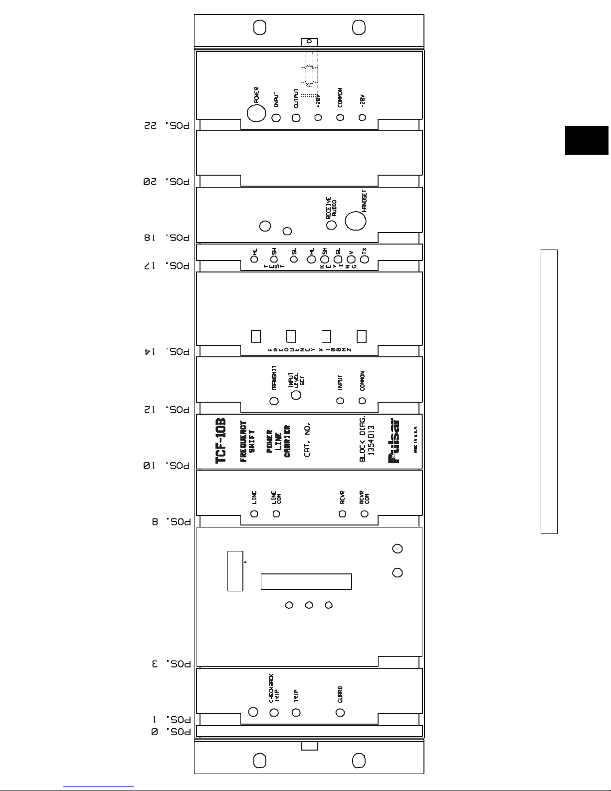
Figure 1–1. TCF–10B Transceiver Set (1355D19).
Technologies, Inc.
GOOD
CHANNEL
MANUAL
CF44
UNIVERSAL RECEIVER
RCVR LOGIC
RF INTERFACE
C2N1B2END
TRANSMITTER
VOICE ADAPTER
CALLING
P. B .
ALARM
EM. OUTPUT
POWER SUPPLY
KEY
10W POWER AMP
CANCEL / RAISE
kHz
LOWER
SET
+10
+5
–10
–15
–20
–5 dB
0
FSK:
LOW
NOISE
SIGNAL
AM: MARGIN
DETECT
1
Page 20

Figure 1–2. TCF–10B Transmitter (only) Set (1355D19).
Technologies, Inc.
Page 21

1
Figure 1–3. TCF–10B Receiver (Only) Set (1355D19).
Technologies, Inc.
GOOD
CHANNEL
MANUAL
CF44
UNIVERSAL RECEIVER
RCVR LOGIC
RF INTERFACE
EM. OUTPUT
POWER SUPPLY
CANCEL / RAISE
kHz
LOWER
SET
+10
+5
–10
–15
–20
–5 dB
0
NOISE
LOW
SIGNAL
FSK:
AM:
MARGIN DETECT
Page 22

Page 1–8 December 2004
TCF–10B System Manual
Te chnologies, Inc.
RCVR LOGIC
CHECKBACK
TRIP
GOOD
CHANNEL
UB/POTT
TRIP
DTT TRIP
GUARD
RCVR LOGIC
GOOD
CHANNEL
TRIP
POSITIVE
TRIP
NEGATIVE
Figure 1–4.
Front Panel for 2-Frequency,
Transfer Trip or Unblock
Applications.
Figure 1–6.
Front Panel for 2-Frequency,
Phase Comparison
Applications.
Figure 1–5.
Front Panel for 3-Frequency,
Transfer Trip and Unblock
Applications.
Page 23

22.5 mV (min) to 70 V (max) 5 mV (min) to 17 V (max)
-20 dBm to +50 dBm @ 50 Ω -35 dBm to +38 dBm @ 50 Ω
Receive Sensitivity
Standard Setting High Setting
1.8 Specifications
The TCF–10B meets or exceeds all applicable ANSI/IEEE standards as follows:
Proposed American National Standard
Requirements for Single Function Power-Line Carrier
Transmitter/Receiver Equipment
(ANS C93.5)
1.8.1 System
Table 1-1 lists the system specifications for the TCF–10B.
December 2004 Page 1–9
Chapter 1. Product Description
1
Frequency Range 30—535 kHz in 0.5 kHz (500 Hz) steps; transmitter selection in
100 Hz steps
4-Wire Receiver Input Impedance 5,000 Ω (1,000 Ω when strapped for high sensitivity)
RF Input Impedance Nominal unbalanced 50 Ω, 75 Ω or 100 Ω
Output Power 10 W (max), 0.1 W (min), 50 or 100 W (with optional external
amplifier)
Modulation Type Frequency-Shift Keyed (FSK); strappable for either two- or
three—frequency operation
Frequency Shift Narrow Shift (– 100 Hz)
Wide Shift (– 250 Hz)
Extra Wide Shift (– 500 Hz)
Nominal Receiver Bandwidths Narrow Band (380 Hz at 3 dB points)
Wide Band (800 Hz at 3 dB points)
Extra Wide Band (1,600 Hz at 3 dB points)
In-Band SNR w/o voice 13 dB
w/voice 30 dB
Table 1–1. System Specifications.
Page 24

Frequency Spacing:
(For channels without voice; depends on application.)
Narrow Band Unblock or Transfer Trip (1-way, 500 Hz)
(2-way, 1,000 Hz)
Wide Band (Narrow or Wide Shift) Unblock or Transfer Trip (1-way, 1,000 Hz)
(2-way, 2,000 Hz)
Phase Comparison (SKBU-2A) (1-way, 1,500 Hz)
(60 Hz sq. wave keying) (2-way, 3,000 Hz)
Phase Comparison (SPCU-1A) (1-way, 2,000 Hz)
(60 Hz 3ms pulse keying) (2-way, 4,000 Hz)
Extra Wide Band Unblock or Transfer Trip (1-way, 2,000 Hz)
(2-way, 4,000 Hz)
Phase Comparison (SKBU-2A) (1-way, 2,000 Hz)
(60 Hz sq. wave keying) (2-way, 4,000 Hz)
Phase Comparison (SPCU-1A) (1-way, 2,000 Hz)
(60 Hz 3ms pulse keying) (2-way, 4,000 Hz)
Channel Speed Receiver set for
15 dB margin:
Narrow Band 7.5 ms*
Wide Band 5.9 ms*
Extra Wide Band 4.7 ms*
Page 1–10 December 2004
TCF–10B System Manual
Te chnologies, Inc.
Table 1–1. System Specifications (Cont’d).
All Voice Applications Minimum Channel Spacing (2-way, 4,000 Hz)
(See Section 1.8.10)
1-way represents transmitter to transmitter or receiver to receiver
2-way represents transmitter to receiver
* Times do not include logic trip delay or relay operate times.
† An external hybrid or other device offering at least 20 dB rejection of the adjacent channel must be used in the application.
Page 25

1.8.2 Alarm & Level Options
This section provides three tables depicting the alarm and level options, broken down as follows:
•Transceiver Chassis Alarms w/CLI
• Receiver Only Chassis Alarms w/CLI
•Transmitter Only Chassis Alarms
Each alarm contact is rated 10 VA (Form A or B).
December 2004 Page 1–11
Chapter 1. Product Description
1
Table 1–2. Transceiver Chassis Alarms w/CLI.
Power Supply Module Loss of dc power
Keying Module Shift High/Shift Low (for guard or trip)
10W PA Module Loss of Transmitter RF power output
Universal Receiver Module Low-Signal; RF Signal Received; CLI output for External CLI
Meter (-20 dB to +10 dB; 0—100 A)
Table 1–4. Transmitter Only Chassis Alarms.
Power Supply Module Loss of dc power
Keying Module Shift High/Shift Low
10W PA Module Loss of Transmitter RF power output
Table 1–3. Receiver Only Chassis Alarms w/CLI.
Power Supply Module Loss of dc power
Universal Receiver Module Low-Signal; RF Signal Received; CLI output for External CLI
Meter (-20 dB to +10 dB; 0—100 A)
Page 26

1.8.3 Electro-Mechanical Outputs
This section provides two tables depicting the Electro-Mechanical Output Module’s specifications, broken
down as follows:
• Electro Mechanical Outputs
• Electro Mechanical Output Timing
Page 1–12 December 2004
TCF–10B System Manual
Te chnologies, Inc.
1.8.4 Keying
Table 1-7 shows the TCF–10B keying specifications.
Contacts Output
Six (6) contacts for Guard Make and carry rated 30 A for 1 second; 10 A continuous capability
or Trip 1 or Trip 2 break 50 W resistive or 25 W with L/R = .045 seconds
Typical Operate Time Typical Release Time
NO Contact NC Contact NO Contact NC Contact
Closes Opens Opens Closes
3.0 ms 2.0 ms 2.8 ms 3.8 ms
3.0 ms bounce 4.0 bounce
Table 1–5. Electro Mechanical Outputs.
Table 1–6. Electro Mechanical Output Timing.
Five (5) optically-isolated keying inputs, 1) Unblock or Phase Comparison
strappable at 15/20, 48, 125, 250 Vdc 2) Direct Transfer Trip
3) Power Boost or 52b Keying
4) RF Power On/Off
5) Voice Adapter
Maximum input keying burden 10 mA
Manual keying Recessed push-button switches for high-
and low-frequency keying, and power boost
Table 1–7. Keying Specifications.
Page 27

1.8.5 Transmitter
Table 1-8 shows the TCF–10B transmitter specifications.
1.8.6 Receiver
Table 1-9 shows the TCF–10B receiver specifications.
December 2004 Page 1–13
Chapter 1. Product Description
1
NOTE
An optional 20 V Power Supply is available for use with some Phase
Comparison and some Directional Comparison systems. For further information, please see TCF–10B Accessories under Chapter 2, Applications.
Harmonic and Spurious Output 55 dB below 10 W
Output Variation – 1 dB over temperature and voltage range
Frequency Stability: – 10 Hz
Narrow Shift
Wide Shift
Extra Wide Shift
Frequency Stability: – 10 Hz
Narrow Band, Narrow Shift
Wide Band, Narrow Shift
Wide Band, Wide Shift
Extra Wide Band, Extra Wide Shift
Five 1 A isolated outputs for 15/20 Vdc 1) Unblock or Trip or Trip-Positive
or station battery circuits 2) Low-Level or Low Signal
3) Guard or Trip-Negative
4) Noise
5) Checkback Trip (not used with
Phase Comparison)
Table 1–8. Transmitter Specifications.
Table 1–9. Receiver Specifications.
Page 28

1.8.7 Power Requirements
Table 1-10 shows the TCF–10B power requirement specifications.
1.8.8 Weights and Dimensions
Table 1-11 shows the TCF–10B weight and dimension specifications.
Page 1–14 December 2004
TCF–10B System Manual
Te chnologies, Inc.
Permissible ripple on incoming Vdc 5%
Maximum allowable frequency of ripple 120 Hz
Carrier frequency on dc input leads when transmitting 10 W 20 mV (max)
Equipment
Net Weight Height Width Depth Rack
lbs Kg inches mm inches mm inches mm Space
Transceiver 21 9.53 5.25 133.4 19.00 482.6 13.50 342.9 3 RU
Transmitter 14 6.35 5.25 133.4 19.00 482.6 13.50 342.9 3 RU
Receiver 12 5.45 5.25 133.4 19.00 482.6 13.50 342.9 3 RU
Transceiver Supply Current (Amps)
At Nominal Voltage
Nominal Permissible
Battery Voltage Receive/ 1 Watt 10 Watt
Voltage Range Standby Transmit Transmit
48/60 Vdc 38—70 Vdc 0.630 0.940 1.600
110/125 Vdc 88—140 Vdc 0.240 0.360 0.600
220/250 Vdc 176—280 Vdc 0.120 0.180 0.300
Table 1–10. Power Requirement Specifications.
Table 1–11. Weight and Dimension Specifications.
Page 29

1.8.9 Environmental Requirements
This section provides three tables depicting the environmental requirement specifications, broken down as
follows:
• Environmental Requirements
• Altitude Dielectric Strength De-Rating for Air Insulation (Table 1-13)
• Altitude Correction For Maximum Temperature Of Cooling Air (ANS C93.5) (Table 1-14)
December 2004 Page 1–15
Chapter 1. Product Description
1
Ambient temperature range -20 to + 60¡C (derated per Table 1-14) of air-contacting
equipment
Relative humidity Up to 95% (non-condensing) at 40¡C (for 96 hours
cumulative)
Altitude Up to 1,500 m (without derating)
Up to 6,000 m (using Table 1-13 and Table 1-14)
Transient withstand capability All external user interfaces meet SWC specifications of
ANS C37.90.1 (1989)
1-minute withstand Only isolated inputs and outputs, and all alarms:
2,500 Vdc from each terminal to ground, derated per
Table 1-13.
Center conductor of coaxial 3,000 Vdc impulse level, cable to ground using 1.2 x 50
cable to ground msec impulse
Electro-Magnetic Interface Capability IEEE Standard ANS C37.90.2
Table 1–12. Environmental Requirements.
Page 30

Altitude (Meters) Correction Factor
1,500 1.00
1,800 0.97
2,100 0.94
2,400 0.91
2,700 0.87
3,000 0.83
3,600 0.79
4,200 0.74
4,800 0.69
5,400 0.64
6,000 0.59
Page 1–16 December 2004
TCF–10B System Manual
Te chnologies, Inc.
Table 1–13.
Altitude Dielectric Strength
De-Rating for Air Insulation
Temperatures (Degrees C)
Altitude (Meters) Short-Time Long-Time
Difference
From Usual
Usual 1,500 55 40
Unusual 2,000 53 38 2
Unusual 3,000 48 33 7
Unusual 4,000 43 28 12
Table 1–14.
Altitude Correction For Maximum
Temperature Of Cooling Air (ANS C93.5)
Page 31

1.8.10 Voice Adapter Option
Table 1-15 shows the specifications for the TCF–10B Voice Adapter option.
If the Voice Adapter option is included, it will have an independent receiver of 4 kHz bandwidth, regardless of whether the system is operating at 1,600 Hz (extra wide band), 800 Hz (wide band), or 380 Hz
(narrow band).
December 2004 Page 1–17
Chapter 1. Product Description
1
Modulation Amplitude Modulation with compander
Transmission Full-Duplex
Frequency Response 380 Hz to 2,000 Hz
Signaling 370 Hz AM with signaling push-button
Table 1–15. Voice Adapter Option Specifications.
Page 32

Technologies, Inc.
Page 1–18 December 2004
TCF–10B System Manual
Te chnologies, Inc.
USER NOTES
Page 33

Copyright © 2004 Pulsar Technologies, Inc.
Chapter 2. Applications and Ordering Information
2
2.1 Protective Relay
Applications Using
Frequency Shift Carriers
The TCF–10B carrier set is particularly suitable
for the following types of protective relay
systems:
• Directional Comparison Unblocking
• Permissive Overreaching Transfer Trip
(POTT)
• Permissive Underreaching Transfer Trip
(PUTT)
• Dual Phase Comparison Unblocking
• Segregated Phase Comparison Unblocking
• Direct Transfer Trip
2.1.1 Directional Comparison
Unblocking
The Directional Comparison Unblocking systems
transmit a continuous blocking signal, except
during internal faults. The channel is generally a
frequency-shift keyed (FSK) power line carrier.
For an internal fault, the FSK transmitter is shifted
to the “unblock” frequency. The transmitted
power in many applications is normally 1 W,
boosted to 10 W during unblock operation.
The frequency-shift channel is monitored continuously to prevent tripping when a loss of channel
occurs. The carrier receiver logic is shown in
Figure 2-1. Under normal conditions, a block
frequency is transmitted and OR-1 has no input.
Because AND-1 and AND-2 are not satisfied, OR2 is not energized. For an internal fault, the block
frequency is removed. Assuming that the unblock
signal is shorted out by the fault, OR-1 provides a
direct input to AND-2 to satisfy its input requirements for 150 ms. AND-2 inputs to OR-2 to
operate the RR or to provide input to the AND
shown in Figure 2-3. Without an unblock signal,
150 ms is allowed for tripping. After this period,
lock out is initiated as one of the inputs to AND-2
is removed. This resets the RR or removes the
input to AND. If the unblock signal is received, it
inputs directly to OR-2 to energize the RR or to
provide input to AND. The unblock signal also
removes an input to AND-1 to stop the timer. A
channel failure (no block or unblock signal)
provides input to AND-1 and, after 150ms, locks
out the relaying and triggers an alarm. The
operation of the scheme shown in Figure 2-3 is
given in Table 2-1 for external and internal faults.
The phase and ground trip fault detectors at both
stations must operate for all internal faults; that is,
they must overreach the remote bus.
The dependability and security of Directional
Comparison Unblocking systems make them the
most attractive of the protective schemes for
transmission lines using power line carrier
channels. Over-tripping is avoided by continuous
blocking and continuous channel monitoring.
Only an external fault
within 150 ms after
channel failure can result
in over-tripping.
The scheme is most
appropriate for twoterminal lines, but is
applicable to multiterminal lines. Separate
channels are required
between each terminal
Block
Frequency
Unblock (Trip)
Frequency
Lockout
To RR or
AND (See
Figure 2-2)
AND
2
AND
1
OR
2
150
0
OR
1
Figure 2–1. Simplified Unblock Receiver Logic.
Page 34

and the remote terminal(s). A sample schematic is
shown in Figure 2-2.
You may conserve frequency spectrum by using a
narrow band frequency shift carrier, but at the
expense of channel speed (see Chapter 1,
Specifications).
Another consideration is an open breaker
situation. When the remote breaker is open for an
extended period of time, the relay system must be
able to trip. The remote relay system sends a trip
signal when detecting a remote open breaker. If
this remote signal is received for 1,000 ms (1 sec)
or longer, the carrier receiver logic interprets this
as an open breaker and allows the local end to trip
Page 2–2 December 2004
TCF–10B System Manual
Te chnologies, Inc.
Breaker 1 Trip Fault Detectors (P1)
Breaker 2 Trip Fault Detector (P2)
Protected Line
G
H
F
I
F
E
Power Line Carrier
Channel f1(G to H)
Power Line Carrier
Channel f2(H to G)
1 2
RR
P
Channel
Signal
Receiver
(F1at H,
F2at G)
RR
Trip
Coil
52a
Contact Logic (per Terminal)
Key Transmitter
to Unblock
Timer
P
Trip
Unblock
(See Figure 2-1)
AND
X
O
Solid State Logic (per Terminal)
Note: (X) Normally 4 Ms.
Figure 2–3. Basic Logic Diagrams for Directional Comparison Unblocking.
Figure 2–2. TCF-10B Transceiver Unit Connections, 2 Freq. set (Directional Comparison Unblock
Relaying) Typical Catalog: C2M1B2SND
TB7-1
TB3-3
TB3-5 TB3-6
TB3-1 TB3-2
TB2-5 TB2-6
TB7-3 TB7-4
TB3-4
TB7-2
Receiver Input
Note: All contacts are link selectable for normally open or closed.
TCF-10B TerminalsRelay Terminals
Line Relay
Keying Output
DC Input
TB1-1
UB Trip
Received
Shift High
Shift Low
Xmtr On
Low Signal
DC Fail
Checkback
Trip
TB1-4 TB1-8 TB4-6
UB Key
Transmitter
TB4-5
Page 35

SCHEME FOR EXTERNAL AND INTERNAL FAULTS
SCHEME FOR EXTERNAL AND INTERNAL FAULTS
Internal (FI) P1operates.
f
1
channel to unblock.
Loss of block and/ or receipt
of unblock (f
2
) operates RR
or inputs AND.
Trip.
P
2
operates.
f
2
channel shifts to unblock.
Loss of block and/or receipt
of unblock (f
1
) operates RR
or inputs AND.
Trip.
Type of Fault Events at Station G Events at Station H
December 2004 Page 2–3
Chapter 2. Applications and Ordering Information
2
Table 2–1. Operation of the Directional Comparison Unblocking Scheme.
External (F
E
) P1operates.
f
1
channel shifts to unblock.
f
2
channel continues to
block.
No trip.
P
2
does not see fault.
Loss of block and/or receipt
of unblock (f
1
) operates RR
or inputs AND.
No trip.
Table 2–2. Operation of the Underreaching Transfer Trip Scheme.
Type of Fault Events at Station G Events at Station H
External (F
E
) P1does not operate.
No channel signal sent to H.
No trip.
P
2
does not operate.
No channel signal sent to G.
No trip.
Internal (F
I
)
(Fault near station H)
P1does not operate.
No channel signal sent to H.
(FD
1
operates).
Transfer-trip (f
2
) from station
H operates RR or inputs to
AND (or OR if non-permissive).
Trip.
P
2
operates and trips
directly.
Transfer-trip signal keyed to
station G.
(FD
2
operates).
Trip.
† Omitted in non-permissive systems.
Page 36
whenever the local relays detect a
fault.
2.1.2 Permissive
Overreaching
Transfer Trip
Systems
Overreaching transfer trip systems
require a channel signal to trip, and
are used with a frequency-shift
audio tone, modulated on a
communication channel (e.g.,
public or private telephone lines).
These systems are generally not
used with power line carriers.
There are, however, successful
applications of power-line carrier
on POTT schemes where parallel
lines allow for cross-coupling of
the carrier signal.
2.1.3 Permissive and
Non-Permissive
Underreaching
Transfer Trip
Systems
For overreaching systems, the
directional phase and ground trip
fault detectors (P) must be set to
overlap within the transmission
line and not overreach any
terminals (see Figure 2-4).
That is, at least one trip fault
detector (P) must operate for all
internal faults, and none should
operate for any external fault. In
practice, distance relays are
normally required for both ground
faults and phase faults, although
directional instantaneous groundovercurrent relays might meet
these requirements in some cases.
Though it is the least complex, the
non-permissive system is rarely
used because of the high potential
for false outputs from the channel,
Page 2–4 December 2004
TCF–10B System Manual
Te chnologies, Inc.
Breaker 1 Trip Fault Detectors (P1)Breaker 1 Permissive Fault Detectors (FD1)
Breaker 2 Trip Fault Detectors (P2)
Breaker 2 Trip Fault Detectors (P2)
Protected Line
G
H
F
I
F
E
1 2
Contact Logic (per Terminal)
P
FD
Trip
Solid State Logic (per Terminal)
Channel
except Power Line Carrier
Audio Tone
Receiver f
2
Audio Tone
Receiver f
1
Audio Tone
Transmitter f
1
Audio Tone
Transmitter f
2
RR
Audio
To ne
Receiver
RR
Trip
Coil
52a
FD P
Key Audio Tone Transmitter
to Remote Station
Key Audio Tone Transmitter
to Remote Station
Key Audio Tone Transmitter
to Remote Station
Audio Tone
Receiver
Omit and Bypass
for Non-Permissive
Schemes
AND OR
Permissive Schemes
Non-Permissive Schemes
P
Trip
Audio Tone
Recovery
OR
Figure 2–4. Basic Logic Diagrams for
Underreaching Transfer Trip Systems.
which would cause incorrect tripping. If a non-permissive system is
used, the channel considerations should be as described later for
direct trip systems. The system is made permissive by the additional
set of phase and ground overreaching fault detectors (FD), which
must operate for all internal faults (see Figure 2-4).
Operation of the underreaching transfer trip scheme shown in
Figure 2-4 is described in Table 2-2 for external and internal faults.
Because the trip fault detectors (P) do not operate for external
faults, underreaching transfer trip systems do not require external
Page 37

fault-clearing coordination circuits (transient blocking) and are,
therefore, inherently simpler than any of the other schemes. You
obtain maximum security if you use additional permissive fault
detectors. These schemes also provide minimum operating times
for many faults that are tripped directly, without using the
channel.
December 2004 Page 2–5
Chapter 2. Applications and Ordering Information
2
Figure 2–5. Basic Operation of the Dual
Phase Comparison Pilot Relaying System.
2.1.4 Dual Phase
Comparison
Unblocking
Systems
Dual comparison systems require a
duplex channel: one frequency for
each line terminal. The TCF–10B
frequency-shift channel equipment
is available for this purpose;
normally used in an unblocking
system. Continuous channel monitoring is also provided, because
either a trip positive or trip
negative carrier signal is always
transmitted.
The transmitter is keyed to its trip
positive frequency when the
square wave from the filter goes
positive, and is keyed to its trip
negative frequency when the
square wave is at zero. There are
two outputs at the receiver: the trip
positive output is a square wave
that goes positive when a trip
positive frequency is received; the
trip negative output goes positive
when a trip negative frequency is
received.
The basic operation of the Dual
Phase Comparison system is
shown in Figure 2-5. For internal
faults, the single phase outputs of
the sequence current networks are
essentially in phase, although such
output represents currents 180°
apart in the power system. The
network output goes through a
squaring amplifier that keys the
frequency shift transmitter. An
adjustable delay circuit delays the
local square wave by a time equal
to the channel delay time.
The network output is then used to
develop two complementary
square waves. One wave, which
has a positive state during the
positive half-cycle of the sequence
Page 38

current network, is compared with the receiver’s
trip positive output. The other wave, which has
positive output during the negative half-cycle of
the sequence current network, is compared to the
receiver’s trip neg. output in a second comparison
circuit.
On internal faults, the positive half-cycle of the
local square wave lines up with the received trip
positive output to provide an AND-1 output (see
Figure 2-5). On the negative half-cycle, this local
square wave lines up with the received trip
negative output to provide an AND-2 output. If an
arming signal is received (FD
2
and/or 21P) and
either AND-1 or AND-2 output exists for 4ms, an
input to the trip flip flop initiates breaker tripping.
The same operation occurs at both terminals,
tripping breakers 1 and 2 simultaneously on either
half-cycle of fault current.
For tripping, both the trip positive and trip
negative frequencies must be transmitted through
the internal fault via power line carrier channels.
If these frequencies are not received, the receiver
detects a loss of channel and clamps both outputs
to a continuous positive state. This loss of channel
clamp enables both comparison circuits, allowing
the system to trip on the local square wave input
only. After 150ms, the system output clamps these
to the zero state. At this point, the system cannot
trip and is locked out. An alarm indicates loss of
channel.
For external faults, the reversal of current at one
end shifts the square waves essentially 180°. As a
result, neither AND-1 nor AND-2 has the
sustained output required to operate the 4ms timer
(see Figure 2-5). No trip occurs at either line
terminal.
2.1.5 Segregated Phase Comparison
System
The Segregated Phase Comparison system has
been developed to improve pilot relay protection,
particularly for the long EHV series capacitorcompensated transmission lines. Long EHV series
capacitor-compensated lines are a source of
significant transients during the fault period.
Under these circumstances, sequence current
networks designed to operate at normal system
frequency may present a problem. The experience
with these Phase Comparison systems has,
however, been remarkably good. Directional
Comparison systems, on the other hand, are
subject to mis-operation on series capacitorcompensated lines, particularly if the capacitor
gaps do not short the capacitors on faults.
Segregated phase comparison systems, which are
current-only, are independent of the following
phenomena:
• Power system frequency and wave form
•Effects of impedance unbalance between
the power system phase circuits.
• Maximum load/minimum fault current
margin.
The segregated phase comparison system can be
divided into two types: a two-subsystem scheme
and a three-subsystem scheme. In the twosubsystem scheme, one subsystem operates from
delta current (I
a-Ib
) for all multi-phase faults, and
a ground (3I
0
) current subsystem operates for all
ground faults. The three-subsystem scheme has a
subsystem for each phase (I
a
, Ib, and Ic). Each
subsystem consists of one channel (TCF–10B)
and one Phase Comparison relay.
Both segregated Phase Comparison systems
incorporate “offset keying,” enabling them to trip
for internal high-resistance ground faults and
internal faults with outfeed at one terminal. No
other system can clear these types of faults
without extra logic or channels. On a 500 kV line
with a 2,000:5 current transformer ratio, for
example, the three-subsystem scheme will operate
for ground-fault resistances up to about 100 Ω
primary impedance. Under the same conditions,
the two-subsystem scheme will operate up to
about 200 Ω primary fault resistance.
The two-subsystem package is suitable for all
applications except single-pole tripping, where the
three-subsystem package must be applied. The
basic operation of the scheme is illustrated in
Figure 2-6. Each current is fed through a noninductive resistor, supplying a voltage output to the
squaring amplifier (SA) that is exactly proportional to the primary currents. The output of these
amplifiers is used to key the individual channels
and, through the local delay timers (LDT), to
Page 2–6 December 2004
TCF–10B System Manual
Te chnologies, Inc.
Page 39

December 2004 Page 2–7
Chapter 2. Applications and Ordering Information
2
SA SA SA SA SA SA
LDT LDTLDT LDT LDTLDT
Channel
Facilities
Station G
Protected Line Station H
a a
b b
c c
1 2
Station G
Protected Line Station H
a a
b b
c c
1 2
Squaring Amplifiers
Logic Square Waves Logic Square Waves
Remote
Square
Waves
Remote Square Waves
a) Three-Subsystem (1a1b1c) System
Local Delay Timers
SA
SA
LDT
LDT
Local Square Waves Local Square Waves
Remote Square Waves Remote Square Waves
b) Two-Subsystem (IaIbIG) System
Squaring Amplifiers
Channel Facilities
SA
SA
LDT
LDT
Ia–I
b
Ia–I
b
Figure 2–6. Basic Segregated Phase Comparison Systems.
Page 40

Page 2–8 December 2004
TCF–10B System Manual
Te chnologies, Inc.
provide the local square waves for comparison.
The timers are adjustable between 2 and 20ms to
compensate for the delay time of the channel. This
digital delay circuit translates the pulse train independently of the pulse width ratio, in contrast to
the ac phase angle shift used in the other systems.
The ac phase shift delay uses frequencydependent components, which are accurate only at
system frequency and can “ring” during transient
conditions.
The square wave comparison is made independently for each current in the separate subsystems.
Separate channels are required for each of the
subsystems. One of the comparison circuits is
shown in simplified form in Figure 2-7. In this
dual comparison circuit, AND-P is used for the
positive half-cycles and AND-N for the negative
half-cycles. As shown in Figure 2-7, the received
positive square wave corresponds to a “1” input to
AND-P, and the received negative square wave to
a “0” input, negated to “1”, into AND-N. Except
for this variation, operation is as shown by the
square wave blocks in the lower half of Figure
2-5.
To generate the local and keying square waves,
conventional phase comparison systems use
thresholds equivalent to (or very near) the zero
axis. As a result, an internal fault with outfeed
looks like an external fault to those systems (see
Figure 2-8). The offset keying technique permits
the relay system to trip for internal faults with
outfeed current out at one terminal. While the
outfeed condition is very unusual, it presents
difficult problems to the great majority of pilot
relaying systems when it does occur. Outfeed can
occur in any of the following cases:
• Series-capacitor-compensated parallel
lines.
•Weak-feed or zero-feed applications,
particularly with heavy through load.
• Some multi-terminal applications.
• Series-compensated (line-end compensation) line with a source inductive
reactance smaller than series capacitor
reactance.
• Some single-line-to-ground faults, occurring simultaneously with an open
conductor, where the fault is on one side of
the open conductor.
• Some single-line-to-ground faults with
high fault resistance and heavy through
load (such conditions can cause outfeed
only in the faulted phase current, not in the
ground subsystem).
The offset keying technique allows the relay
system to work like a true current differential
scheme. The scheme takes advantage of the fact
that, for the outfeed condition, the current into the
line is greater in magnitude than the current out of
the line for the internal fault.
This relationship is illustrated in Figure 2-8,
where I
G
equals IFplus IH. While the two terminal
currents may have any angular relationship with
one another, most outfeed conditions display a
nearly out-of-phase relationship. The out-of-phase
condition illustrated is the most difficult case for
phase comparison, as well as the most common
outfeed condition.
In the offset keying technique, the keying
threshold is displaced in the positive direction,
away from the zero axis. The local square wave
thresholds are displaced negatively. To maintain
security, the local thresholds are separated from
each other, providing “nesting” during external
faults. Typical settings are shown in Figure 2-9.
Figure 2-10 illustrates the square wave characteristics of offset keying for normal internal faults,
external faults, and internal faults with outfeed.
The segregated Phase Comparison scheme incorporates a high degree of security. Its design is
based on extensive field experience and the model
line tests for the very long, series capacitorcompensated EHV lines.
Output trip signals are supervised by an arming
input and a number of security checks (see
Figure 2-8). Phase arming is performed by a
current rate-of-change detector that responds to
sudden increases, decreases, or angular shifts in
current. It operates on current changes of 0.5 A or
more, with an operating time of 2 ms. Ground
Page 41

December 2004 Page 2–9
Chapter 2. Applications and Ordering Information
2
AND
P
AND
N
OR
Comparison
AND
Arming Input-Current Detector (CD)
Channel Security Checks
Remote
Square Waves
from Channel
Local
Square
Waves
Positive
Negative
Trip
Note:
X = 3 Milliseconds for the Phase Subsystems
4 Milliseconds for Ground
X
0
Figure 2–7. Basic Operation of the Segregated Phase Comparison System.
I
F
I
G
I
H
Outfeed for an Internal Fault (See Text)
Fault
Local
Square Wave
Remote
Square Wave
External Line Up
Note: Comparison at Both Terminals sees Fault as External.
Keying
Square
Wave
Figure 2
–
8. Conventional Phase Comparison Response to an Outfeed Condition Block Tripping.
Typical Settings
+3A
-2A
-4A
Trip Positive
Trip Positive
Trip Negative
Trip Negative
Local Positive
Local Positive
Local Negative
Local Negative
1
0
1
0
Keying Square Wave
Zero Axis
I
Key
(1)
(0)
(0)
(1)
Figure 2–9. Typical Threshold Setting for Offset Keying.
Page 42

arming is 3I magnitude—typically
0.8 A secondary.
Security checks to comparison
AND (see Figure 2-8) include (1)
low channel signal blocking, (2)
lockout for sustained low channel
signal, (3) channel noise clamp,
and (4) receive guard block. For
the phase subsystems, a trip signal
occurs if comparison AND has an
output for more than 3ms (4ms for
the ground subsystem).
2.2 Direct TransferTrip Systems
Direct transfer-trip systems
provide circuit-breaker tripping at
remote or receiver terminals,
without any supervision by fault
detectors. The most important
consideration in a direct transfertrip system is the type of channel
applied. The communications
equipment must carry the total
burden of system security and
dependability.
Direct transfer-trip systems are
applied for:
• Line protection with nonpermissive under reaching
transfer-trip systems.
•Transformer protection
where there is no circuit
breaker between the transformer and transmission
line.
• Shunt reactor protection.
• Remote breaker failure
protection.
A sample schematic is shown in
figure 2-11.
Page 2–10 December 2004
TCF–10B System Manual
Te chnologies, Inc.
Trip Positive
Trip Positive
Trip Negative
Trip Negative
Local Positive
Local Positive
Local Negative
Local Negative
F
Internal Line Up
Keying
Square
Wave
G
H
1
0
1
0
Trip Coincidence
Remote Square Wave
Shaded Portion is
Trip Coincidence
Note:
Similar Comparison Occurs
at Terminal H.
a) Normal Internal Fault
Trip Positive
Trip Positive
Trip Negative
Trip Negative
Local Positive
Local Positive
Local Negative
Local Negative
I
Key
F
Internal Line Up
Keying Square Wave is
Steady Trip Negative
G
H
1
0
1
0
Trip Coincidence
Remote Square Wave Shaded Portion is
Trip Coincidence
Note:
Similar Comparison Occurs
at Terminal H.
c) Internal Fault with Outfeed (Comparison at Strong Terminal)
Keying
Square
Wave
Trip Positive
Trip Positive
Trip Negative
Trip Negative
Local Positive
Local Positive
Local Negative
Local Negative
I
Key
F
External Line Up
G
H
1
0
1
0
Trip Coincidence: None
Remote Square Wave
Note:
Similar Comparison Occurs
at Terminal H.
b) External Fault
Note:
Local Square
Waves "Nest" within
Remote Square Wave
to Provide Security
Figure 2–10. Response of Segregated Phase Comparison
System with Offset Keying.
Page 43

December 2004 Page 2–11
Chapter 2. Applications and Ordering Information
2
Figure 2–11. TCF-10B Transceiver Unit Connections 2 Freq. set (Single Channel Direct Transfer Trip) Typical Catalog: C2N1B2END
Page 44

2.2.1 Transformer Protection
A typical transformer protection scheme is illustrated in Figure 2-12. A direct trip channel is
keyed to the trip state when the transformer
protective relays operate. The received trip signal
will then trip the remote end breaker and lock out
reclosing.
Although it is no longer widely used, you may use
a ground switch operated by the transformer
protective relays for transformer protection. In
this technique, a ground fault is initiated on the
transmission line at G, providing adequate fault
current for the ground relays at H to trip the
breaker at H. This system is slower but is widely
used on lower voltage systems and is fairly simple
and straightforward. It does not require any secure
communication medium between G and H. For
this type of application, the ground relays at H can
be set to operate for 100 percent of the line and not
overreach to bus G.
While a single switch on one phase is normally
applied, you may use a double switch on two
phases to initiate a double-phase-to-ground fault.
In the latter case, both phase and ground relays
can operate to ensure redundancy. Fault grounding
is not applicable to all systems because of high
short-circuit capacity.
2.2.2 Shunt Reactor Protection
Shunt reactors are frequently used on HV and
EHV lines. These line reactors are connected on
the line side of the circuit breakers (see
Figure 2-11). A remote trip channel is thus
required for a fault in the shunt reactor.
2.2.3 Remote Breaker-Failure
Protection
A remote breaker-failure system is necessary
where a multi-breaker bus, such as a breaker-anda-half or ring bus scheme, is applied at a
transmission line terminal. A direct transfer-trip
system will be a part of the remote breaker-failure
protection.
2.2.4 Direct Trip Channel
Considerations
The channel and its terminal equipment are major
factors in the proper operation of the direct
transfer-trip system. The channel must neither fail
to provide a correct trip signal nor provide a false
signal.
While other types of modulation are possible,
frequency-shift keyed (FSK) equipment offers the
best compromise between noise rejection capability and equipment complexity. Two frequencies
are usually transmitted in an FSK system: the
“guard” frequency is transmitted during non-trip
conditions and the “trip” frequency is transmitted
when a breaker trip is required. Because a signal
is always present, the FSK system will allow the
channel to be continuously monitored. Continuous
channel monitoring is necessary in a direct trip
Page 2–12 December 2004
TCF–10B System Manual
Te chnologies, Inc.
Direct Transfer Trip Channel
87
G H
Transformer Bank
Transmission Line
DTT
52c
52
TC
+
–
Figure 2–12. Direct Transfer Trip for
Transformer Protection.
Bi-Directional Direct
Transfer Trip Channel
––
DTTDTT
52a52a
52
TC
52
TC
++
Shunt Reactor
Protection
87.50/51.63, etc.
Figure 2–13. Direct Transfer Trip for
Shunt Reactor Protection.
Page 45

December 2004 Page 2–13
Chapter 2. Applications and Ordering Information
2
system, because breaker tripping is not supervised
by any local relays.
As noise in the channel increases, a point is
reached where there is a high probability of false
tripping. The level of noise at which the channel
becomes unreliable must be determined by tests.
Signal-to-noise ratio monitors must then be
included with any direct trip channel, to block
possible false tripping. It is important, however,
not to get the noise monitors any more sensitive
than required, since their operation will prevent
tripping.
There are three important aspects to the application of FSK channels to direct trip systems:
channel bandwidth, dual channel systems, and
channel protection.
Although faults should be cleared in the shortest
possible time, speed is not the only criterion for
selecting equipment. It is important to use the
narrowest bandwidth equipment possible. A wide
bandwidth channel may give the desired speed,
but more noise enters the system. Thus, the
channel will block tripping sooner than a narrower
bandwidth channel with the same received signal
level. A wideband channel will consequently not
be as dependable as a narrower channel under
equal receive-level conditions.
A dual channel system is recommended for direct
trip applications. Two FSK channels should be
used in series, so that both must trip before the
breaker is tripped. Many tests have indicated that
dual channels improve the security of the direct
trip system by several orders of magnitude. Use of
a dual channel system has very little effect on
dependability, even if both channels are on the
same transmission medium.
If you want to increase the dependability, you can
modify the dual channel transfer trip scheme to
allow a single channel trip when there is failure of
the other channel. A typical Dual Channel
Throwover to Single Channel Scheme is illustrated in Figures 2-14 & 2-15.
2.3 Special Considerations
The TCF–10B frequency-shift equipment can
operate in either the two- or three-frequency
mode, but ordinarily operates as a two-frequency
system. The three basic frequencies are as follows
(see Figure 2-16):
f
C
Center frequency
TB6-1
TB6-2
Channel 1 DTT
TB2-5
TB2-6
TB6-2
TB6-1
TB2-6
Loss of Channel 1
Loss of Channel 2
Channel 2 DTT
TB2-5
LOR
(–)
(+)
Figure 2–14.
Dual Channel Direct Transfer Trip with Throwover
to Single Channel.
TB6-1
TB6-2
Channel 1 DTT
Channel 1 DTT
TB2-5
TB6-3
TB2-6
TB6-4
TB6-2
TB6-4
TB6-1
TB6-3
TB2-6
Loss of Channel 1
Loss of Channel 2
Channel 2 DTT
Channel 2 DTT
TB2-5
LOR
(–)
(+)
Figure 2–15.
Dual Channel Direct Transfer Trip with Throwover
to Single Channel.
Page 46

fHHigh-frequency, is a frequency shift (∆f)
above f
C
fLLow-frequency, is a frequency shift (∆f)
below f
C
The value of ∆f depends on the bandwidth of the
TCF–10B set. For a bandwidth of 1600 Hz, ∆f is
500 Hz. A bandwidth of 380 Hz yields a ∆f of
100 Hz, while the 800 Hz bandwidth ∆f can be
either 250 or 100 Hz, depending on the setting of
S5 on the Transmitter Board. The center channel
frequency (f
C
) can vary from 30 to 535 kHz (in
0.5 kHz steps).
In the two-frequency systems, only f
H
and fLare
used. The two frequencies function differently and
take on different labels when operating with the
different types of protective relay systems.
2.3.1 Directional Comparison
Unblocking (Two-Frequency)
The higher frequency (fH), or “Guard” frequency,
is transmitted continually as a blocking-type
signal during normal conditions, to indicate that
the channel is operative and to prevent remote
relay tripping when external faults occur.
For a fault sensed by the local overreaching pilot
relay, the transmitter is frequency-shifted to a low
frequency (f
L
), called “Unblock” frequency. The
transmitted power is normally 1 W, boosted to
10 W for the “Unblock” operation.
The Directional Comparison Unblocking system
will generally use the wide band, wide shift (800
Hz BW, ±250 Hz Shift) TCF–10B carrier set.
Also, the most common power output level used
will be the 1 watt block and 10 watt trip. The type
of carrier applied with this scheme may be varied
from the normal for special circumstances, e.g.,
when matching the new TCF–10B equipment at
one end of the line with the older TCF, TCF-10, or
TCF-10A equipment at the other end. In this case,
you must apply the wide band, narrow shift carrier
(800 Hz BW, ±100 Hz Shift) to match the older
carrier characteristics.
2.3.2 Transfer Trip: Overreaching,
Underreaching or Direct (TwoFrequency)
The higher frequency (fH), or “Guard” frequency,
is transmitted continually during normal conditions. For a fault sensed by the overreaching (or
underreaching) pilot relay, the transmitter is
shifted to the low frequency (f
L
), called “Trip”
frequency.
When using the TCF–10B for any permissive
overreaching or underreaching line relay system,
you can apply any bandwidth set. However, the
best all around set to use will be the wide band,
wide shift (800 Hz BW, ±250 Hz Shift)
equipment. If signal-to-noise ratio is of concern,
however, you may use the narrow band set; on the
other hand, if relay speed is critical, you may
apply the extra wide band (1600 Hz, ±500 Hz
Shift) equipment. If, in direct transfer trip
systems, security due to S/N is of concern, we
strongly recommend that you apply only narrow
band equipment. In any of these systems, the usual
power level combination will be 1 watt for guard
and 10 watts for the trip signal.
2.3.3 Phase Comparison
Unblocking: Dual or
Segregated (Two-Frequency)
Phase Comparison relays use square wave signals
for operation. The transmitter is keyed to a “Trip
Positive” frequency when the relay square wave
goes positive, and is keyed to a “Trip-Negative”
frequency when the relay square wave is at zero.
The Trip Positive frequency is frequency-shifted
below f
C
; the “Trip Negative” frequency is
frequency-shifted above f
C
. Either frequency can
function as a trip or block, depending on the local
square wave.
For Phase Comparison systems, you can use only
the wide band with wide shift or extra wide band
TCF–10B. In the interest of conserving spectrum,
the wide band, wide shift channel is most
common. However, if speed is important, you may
apply the extra wide band set. The most often
applied power level will be 10 watts for both
“Trip-Positive” and “Trip-Negative”.
Page 2–14 December 2004
TCF–10B System Manual
Te chnologies, Inc.
Page 47

December 2004 Page 2–15
Chapter 2. Applications and Ordering Information
2
2.3.3.1 Phase Comparison Relaying and
20V Auxiliary Power Supply
When ordering a TCF-10B for use with phase
comparison relaying, a 20V auxiliary power
supply is provided.
The majority of interfaces between the relay and
the communications equipment are done at the
station battery. If the control battery is 125 Vdc,
then the carrier output will be powered up with
125 Vdc to provide station battery voltage to the
relay. However, in phase comparison relay
systems, the ratio, of the on and off state, of the
carrier circuit ouptut and the on and off state of the
relay’s keying circuit is critical to provide a square
wave that closely represents the power system ac
wave. Therefore, based on the type of inputs used
on the relay system at the point it interfaces with
the carrier system, this will determine what
voltage level is acceptable. This criticality is on
the order of 500 or less microseconds.
Due to the capacitors typically applied to output
circuits to dampen surges, the higher the voltage
applied, the longer it will take to dissipate the
energy. Therefore, to dissipate this energy quickly,
to adhere to the timing requirements for a secure
phase comparison relay system, the use of the
auxiliary 20V power supply is necessary.
Different relay manufacturers’ input circuits may
vary and can conceivably decay fast enough not to
hinder the security of the relay system operation.
However, the energy dissipated will also generate
a significant amount of heat. By utilizing the
auxiliary supply, mounted on the rear of the
carrier unit, it will allow that heat to be outside of
either unit.
Pulsar strongly recommends the application of the
auxiliary power supply for two reasons; decay
time of the energy, and the heating caused by the
dissipation of energy.
2.3.4 Three-Frequency Systems
The TCF–10B also provides for three-frequency
system applications (see Figure 2-16), e.g.,
Directional Comparison Unblocking with Direct
Transfer Trip, or Permissive Overreaching
Transfer Trip with Direct Transfer Trip. All three
frequencies are closely-controlled discrete
frequencies within the equivalent spacing of a
single wideband or extra wideband channel. In
applying a three-frequency system, the Direct
Transfer Trip keying inputs shifts the channel low
(i.e., –250 Hz for 800 Hz bandwidth) and the
unblock key shifts the channel high (i.e., +250 Hz
for 800 Hz bandwidth).
See figure 2-17 for a sample schematic.
2.3.5 Three terminal line applications.
When a three terminal line protection requires
power line carrier equipment, each terminal must
have one transmitter and 2 receivers, since each
terminal must receive a signal from each of the 2
other ends of the line. Fig. 2-18 is a representation
of the transmitter/receiver complement required to
implement a single function: Hybrids or other
isolation devices are required between transmitters and transmitters to receivers. See the
following section for details.
2.4 Hybrid Applications
The purpose of the hybrid is to enable the connection of two or more transmitters together on one
coaxial cable without causing intermodulation
distortion due to the signal from one transmitter
affecting the output stages of the other transmitter.
Hybrids are also required between transmitters
and receivers, depending on the application. The
hybrid circuits can, of course, cause large losses in
the carrier path and must be used appropriately.
High/low-pass and band-pass networks may also
be used, in some applications, to isolate carrier
f(f–f)
LC
f(f+f)
HC
f
C
Amplitude
DTT Trip
(Trip 1)
Unblock Trip
(Trip 2)
Figure 2–16. TCF–10B 3-Frequency System.
Page 48

Page 2–16 December 2004
TCF–10B System Manual
Te chnologies, Inc.
Figure 2–17. TCF-10B Transceiver Unit Connections 3 Frequency Set
(Unblock Relaying and Direct Transfer Trip) Typical Catalog: C2M1B3END or C2M1B3ETD
Page 49
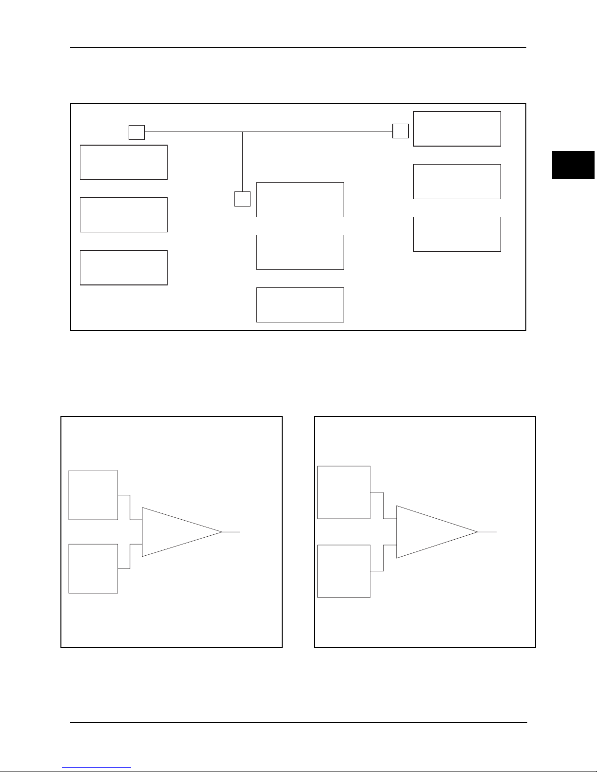
December 2004 Page 2–17
T1
T2
XHybrid
To Line
Tuner
Figure 2–19. Hybrid Connections – Two
Transmitters.
Figure 2–18. Three terminal line application.
T1
R1
X Hybrid
To Line
Tuner
Figure 2–20. Hybrid Connections – Single Bi-
Directional Channel.
F2
A
B
C
F1
F3
F3
F2
F1
F1
F2
F3
Transmitter
Receiver
Receiver
Transmitter
Receiver
Receiver
Transmitter
Receiver
Receiver
Chapter 2. Applications and Ordering Information
2
Page 50

equipment from each other. Several typical applications of hybrids are shown in the following
diagrams, Figures 2-19 through 2-23. A summary
of some of the more important application rules
are given below:
1. All hybrids in a chain should be resistive
type hybrids except the last hybrid, that is,
the one connected to the line tuner.
2. The last hybrid in the chain should be the
reactance type hybrid or a skewed type.
3. When applying transmitters to reactance
type hybrids, the frequency spacing
between the widest spaced transmitters is
about 4% for frequencies below 50 kHz
and 6% for frequencies above 50 kHz. If
this rule is not followed then the hybrid
cannot be adjusted to provide the best
possible isolation between all transmitters.
4. When applying transmitters and receivers
to a reactance type hybrid the frequency
spacing between the transmitter group and
receiver group is of no concern; however,
all the transmitter frequencies must meet
the frequency spacing rule above. This rule
is based on receivers with high input
impedance.
5. When the last hybrid is a skewed type then
the receiver port should be terminated with
a 50Ω resistor to obtain proper isolation.
Afew guidelines follow in order of importance:
1. The hybrids should be arranged with the
lesser losses in the transmitter path and the
greater losses in the receiver path to
provide more transmitter signal levels onto
the power line.
2. Transmitters that are used with wide
bandwidth channels should be arranged
with lower losses and those of narrower
bandwidths should have the higher losses.
3. Narrow band systems are not as susceptible
to noise as wider band systems are,
therefore they can tolerate the higher loss.
If possible, transmitters used for common applications should be arranged for equal attenuation.
This would apply to systems that use dual
channels such as Direct Transfer Trip (DTT) or
Segregated Phase Comparison.
Following are the type of hybrids and their associated style numbers.
2.4.1 Examples
Following are several figures that illustrate
possible hybrid applications. A short description
of each follows.
In these illustrations, Resistive Hybrids are
denoted as R hybrids, Reactive hybrids as X
hybrids and Skewed hybrids as S hybrids. Fig. 219 illustrates two transmitters being combined
onto a single coax cable for connection to a line
tuner. This would be a typical application for a
dual channel, uni-directional trip system. The
receive end of the system would not require a
hybrid so that the receivers would be tied together
via coax cable before connection into the line
tuner.
When only one transmitter and one receiver are
required as in a single channel bi-directional
transfer trip system or a directional comparison
unblocking system Fig. 2-20 can be applied. A
skewed hybrid may be used in place of the
Page 2–18 December 2004
TCF–10B System Manual
Te chnologies, Inc.
• Resistive Hybrid H1RB 6266D72G05
• Skewed Hybrid H1SB-R 1609C45G03
with terminating resistor
• Reactance Hybrid H3XB 6266D71G03
• 19” panel suitable for 3 Hybrids 670B695H01
For details, please refer to the Hybrids System manual, CH44.
Page 51
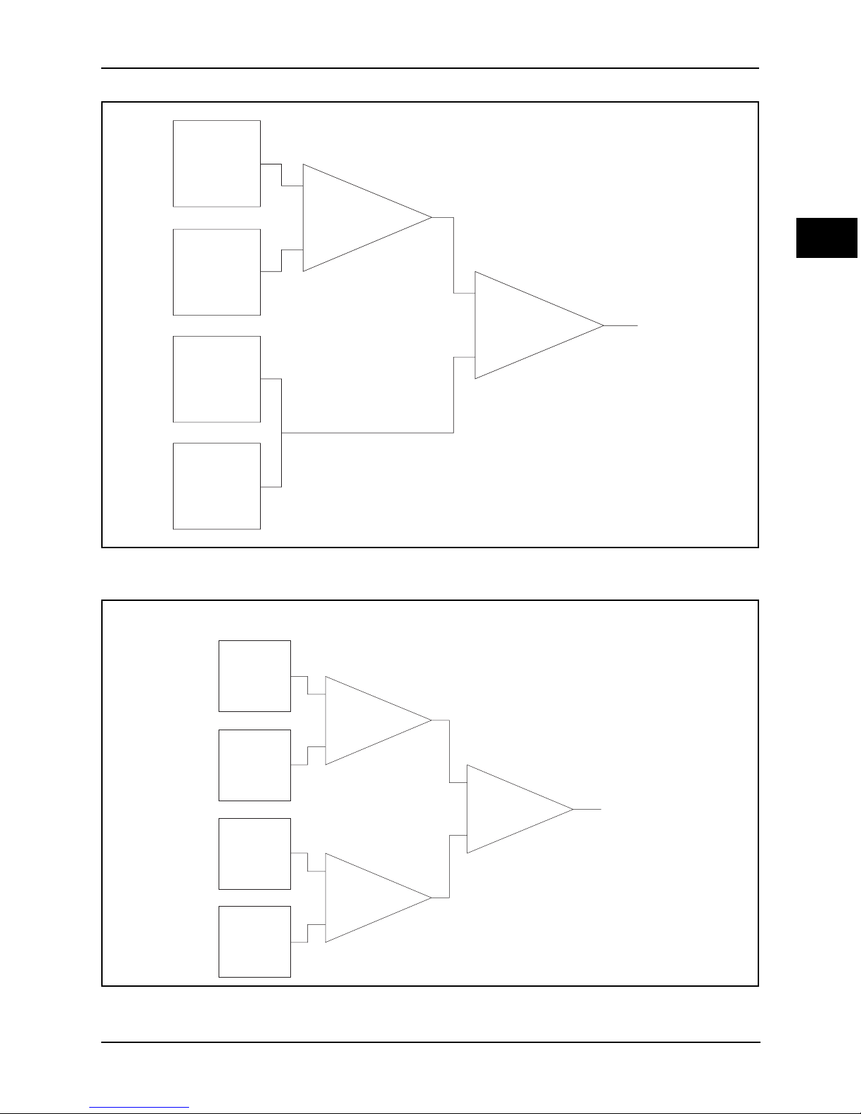
December 2004 Page 2–19
Chapter 2. Applications and Ordering Information
2
T1
T2
R1
R2
X Hybrid
R Hybrid
To Line
Tuner
Figure 2–21. Hybrid Connections – Dual Bi-Directional Channel.
T1
T2
T3
T4
X Hybrid
To Line
Tuner
R Hybrid
R Hybrid
Figure 2–22. Hybrid Connections – Four Transmitters (Equal Losses).
Page 52

Page 2–20 December 2004
TCF–10B System Manual
Te chnologies, Inc.
To Line
Tuner
T1/R1
ON-OFF
T2
WIDE
BAND
FSK
R2
WIDE
BAND
FSK
R3
NARROW
BAND
FSK
R4
NARROW
BAND
FSK
T3
NARROW
BAND
FSK
T4
NARROW
BAND
FSK
RHybrid
RHybrid
RHybrid
XHybrid
Figure 2–23. Hybrid Connections – Four Transmitters (Unequal Losses).
reactive hybrid (X hybrid). The skewed hybrid has
a designated transmit port and receive port.
When two transmitters and two receivers are
being applied to a single coax cable, as in a dual
channel bi-directional direct transfer trip system,
Fig. 2-21 is appropriate.
Four transmitters used for similar applications can
be combined as shown in Fig. 2-22. This would be
representative of two dual channel uni-directional
transfer trip systems. This provides equal losses to
each transmitter.
When different types of modulation and different
bandwidths are utilized, it is better to arrange the
transmitters and receivers as shown in Fig. 2-23.
This allocates loss based on performance factors
of the modulation type and bandwidth.
Page 53
2.5 Ordering Information
The equipment identification number (catalog number) is located in the center of the TCF–10B front panel.
The TCF–10B catalog number comprises nine (9) characters, each in a specific position. This number
identifies the unit’s technical characteristics and capabilities, as well as any optional modules installed in
the unit.
Table 2-4 provides a complete listing of the options for ordering a TCF–10B, as well as a sample catalog
number. To order one or more TCF–10Bs, simply identify the features and optional modules you want for
each chassis. For example, the typical catalog number shown in Table 2-4 — C2N1B2END —
orders a TCF–10B with the following features:
Chassis: Transmitter/Receiver
Transmitter Power Output: 1/10 W
Bandwidth/Frequency Shift: 380 Hz BW ±100 Hz Shift (Direct Transfer Trip)
Power Supply: 110/125 Vdc battery input
Alarms & Carrier Level Indication: with alarms
Channel Type: 2-Frequency
Receiver Output Interface: Electro-mechanical (six contact outputs)
Voice Adapter/Trip Test Unit: No Voice Adapter Module
Receiver Logic: Directional Comparison (Unblock, POTT, PUTT, DUTT, or Direct Transfer Trip)
The TCF–10B accessories are listed in Table 2-3.
December 2004 Page 2–21
Chapter 2. Applications and Ordering Information
2
Other Accessories Module Style Number
20 Volt Power Supply
†
48 Vdc 1610C07G01
125 Vdc 1610C07G02
250 Vdc 1610C07G03
TC–10B/TCF–10B Extender Board 1353D70G01
Accessories for Voice Adapter Module Style Number
Sonalert (2,900 Hz, 60–250 Vdc) SC250J
Telephone Hook switch 205C266G01
Assembly (panel mounting) with
Noise Cancelling Handset
(single prong plug)
Telephone Handset, Noise Cancelling 1353D88G02
Table 2–3. TCF–10B Accessories.
†(For use with some phase comparison relaying equipment or older solid state equipment.)
Page 54
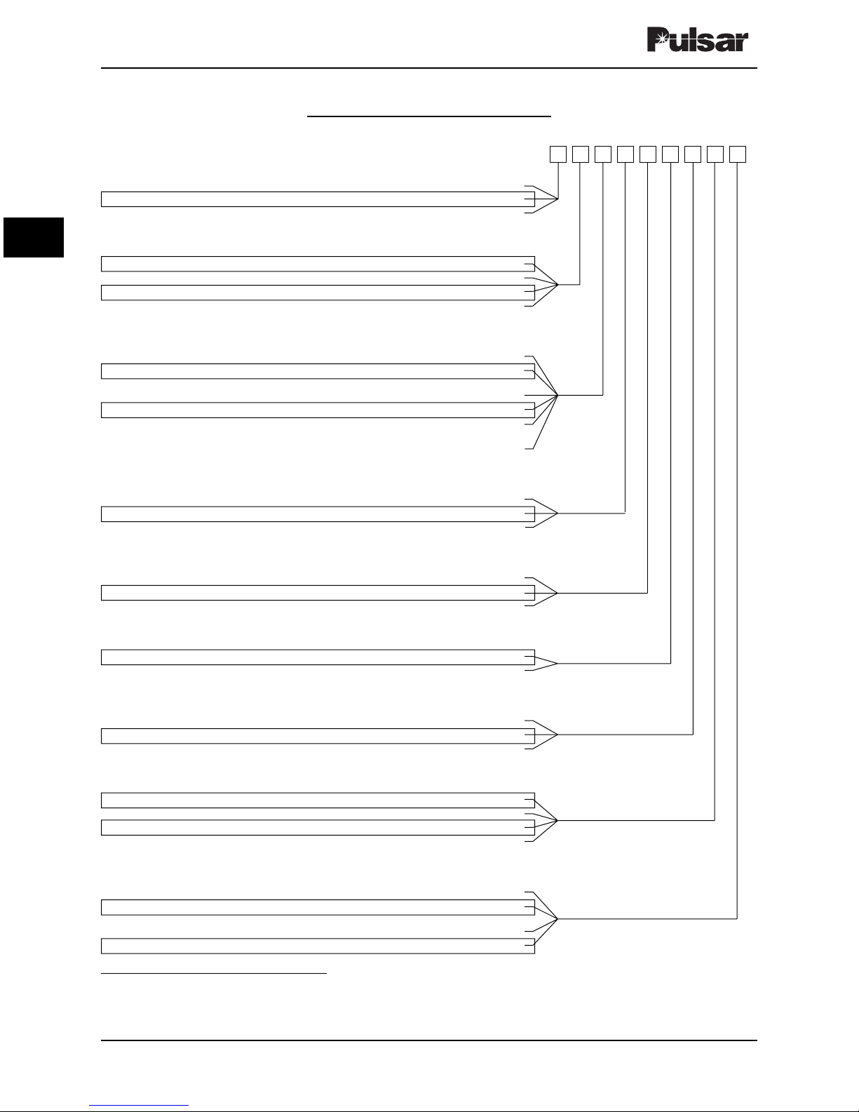
Page 2–22 December 2004
TCF–10B System Manual
Te chnologies, Inc.
Chassis
Transmitter only T
Universal Receiver S
Transmitter/Universal Receiver C
Transmitter Power Output*
1/1 watt 1
1/10 watt 2
10/10 watt* 3
None (Receiver-only chassis) 6
Bandwidth/Frequency Shift
380 Hz BW –100 Hz Shift DOWN (Direct Transfer Trip) N
380 Hz BW –100 Hz Shift UP (Direct Transfer Trip) U
800 Hz BW –100 Hz Shift
(Line relaying, use when matching up with existing
wideband TCF, TCF—10, or TCF—10A carrier at the remote end of the line)
W
800 Hz BW –250 Hz Shift
(Line relaying)
M
1,600 Hz BW –250 Hz Shift
(Phase comparison line relaying P
1,600 Hz BW –500 Hz Shift
(Directional comparison line relaying,
use when a higher than normal speed channel is desired)
X
Power Supply
48/60 Vdc battery input 4
110/125 Vdc battery input 1
220/250 Vdc battery input 2
Alarms and Carrier Level Indication
Transmitter alarms only T
Receiver alarms and CLI only R
Transmitter and Receiver alarms with CLI B
Channel Types
2-Frequency 2
3-Frequency
(Directional comparison line relaying plus transfer trip)
3
Receiver Output Interface
Solid state
(Transistor outputs) S
Electro-mechanical
(six contact outputs) E
No outputs
(Transmitter-only chassis)
N
Voice Adapter / Trip Test Unit
Voice Adapter Module** V
No Voice Adapter Module N
Voice Adapter Module with Trip Test Unit** W
Trip Test Unit w/o Voice Adapter Module T
Receiver Logic
Directional Comparison
(Unblock, POTT, PUTT, DUTT, or Direct Transfer Trip)
D
Phase Comparison P
Telemetry
(Slow speed Direct Transfer Trip; contains no noise processing or
channel logic; not recommended for line relaying applications)
T
No logic
(Transmitter-only chassis) N
Table 2–4. TCF–10B Catalog Numbers
Typical Catalog Number
C 2 N 1 B 2 E N D
Catalog Number Position 123456789
*For 50 or 100 watt output, see Accessories
**Available in Transmitter/Receiver chassis only.
Page 55

December 2004 Page 2–23
Chapter 2. Applications and Ordering Information
2
Figure 2–24. 20 Vdc Auxiliary Power Supply (1610C07; Sheet 1 of 2).
Technologies, Inc.
Page 56

Te chnologies, Inc.
C
2N1
B2END
U
S
C
CF20-RXLMN-001
CF20-RXLMN-003
CF20-RXLMN-002
C020-RXVMN-202 or 203
1606C50G03
C020-VADMN-001
POWER SUPPLY 48V WITH ALARM RELAY
POWER SUPPLY125V WITH ALARM RELAY
POWER SUPPLY250V WITH ALARM RELAY
FSKRECEIVER /DISCRIMINATOR
SHIFT UP TOTRIP
T, S , C
4,1, 2
S,E, N
2,3
T, R , B
D,P,T,N
V, N , W, T
N,U, M,W,P,X
= item selected
Figure 2–25. TCF–10B Catalog Numbers/Module Style Numbers (1355D19)
Page 57
Copyright © 2004 Pulsar Technologies, Inc.
Chapter 3. Installation
3
3.1 Unpacking
If the TCF–10B is shipped unmounted, it is
packed in special cartons that are designed to
protect the equipment against damage.
3.2 Storage
If you are setting the equipment aside before use,
be sure to store it in its special cartons (in a
moisture-free area) away from dust and other
foreign matter.
3.3 Installation Location
Install the TCF–10B in an area which is free from:
•Temperature exceeding environmental
limits (See “Environmental Requirements”
in Chapter 1)
• Corrosive fumes
• Dust
•Vibration
3.4 Assembly
You can assemble the TCF–10B for use either in
one of the following configurations:
• Mounted in a fixed-rack cabinet.
• Mounted in a swing-rack cabinet
• Mounted on an open rack.
or in your own, customer-specified configuration.
Refer to Figure 3-3 for mounting dimensions.
3.5 TCF–10B Rear Panel
Connectors
The following connectors are accessible from the
Rear Panel (See Figure 3-1 and Figure 3-4):
•Terminal Blocks.
• Cable Jacks
• Jumpers
• Input/Output Pins
!
CAUTION
IF YOU ARE USING THE TCF-10B WITH A
SWING-RACK CABINET, MAKE SURE THAT
THE CABINET IS FIRMLY FASTENED BEFORE
OPENING THE RACK (TO PREVENT TIPPING).
NOTE
Low-powered microprocessor relays housed in a solid metal case do not allow for the necessary
air circulation. If you are using this type of relay, make sure you provide one rack unit (1 RU) of
space on the top and bottom of the carrier set to ensure proper air circulation.
!
CAUTION
UNPACK EACH PIECE OF EQUIPMENT
CAREFULLY SO THAT NO PARTS ARE LOST.
INSPECT THE CONDITION OF THE TCF-10B AS
IT IS REMOVED FROM ITS CARTONS. ANY
DAMAGE TO THE TCF-10B MUST BE
REPORTED TO THE CARRIER. DAMAGES ARE
THE RESPONSIBILITY OF THE CARRIER, AND
ALL DAMAGE CLAIMS ARE MADE GOOD BY
THE CARRIER. PLEASE SEND A COPY OF ANY
CLAIM TO PULSAR TECHNOLOGIES, INC.
Page 58

Figure 3–1. TCF–10B Rear Panel (C020-BKPMN/1610C07).
Technologies, Inc.
POS 22
POS 20
POS 18
POS 17
POS 14
POS 12
POS 8
POS 5
POS 3
POS 1
J13
C28
C27
C29
C26
CARRIER MOTHERBOARD
C020BKPMN-001 REV 03
SCHEMATIC C030BKPMN
PC BOARD C050BKPMN REV 02
Power Supply
mounted on rear of Chassis
Page 59

3.5.1 Terminal Blocks
(Refer to Figure 3-4 for further information.)
TB7 Power Supply (Terminals 1 thru 6)
TB6 EM Output (Terminals 1 thru 9)
TB5 Voice Adapter (Terminals 1 thru 9)
TB4 Keying (Terminals 1 thru 6)
TB3 10W PA (Terminals 1 thru 6)
TB2 CLI and (Terminals 1 thru 6)
Discriminator
TB1 Receiver Logic (Terminals 1 thru 9)
3.5.2 Cable Jacks
J1 RF Interface module Transmitter, RF
output line, thru 2-wire coaxial cable
(UHF)
J2 RF Interface module Receiver, RF input
line thru 5,000Ω 4-wire coaxial cable
(BNC)
3.5.3 Jumpers
JU1 UHF Chassis Grd (for J1 not installed)
JU2 BNC Chassis Grd (for J2 not installed)
3.5.4 Input/Output Pins
Pins labeled C and A provide 16 input/output
connections per module (using even numbers 2
through 32 for all modules) as follows:
• Power Supply (pins are to right of TB7)
• EM Output (pins are to right of TB6)
•Voice Adapter (pins are to right of TB5)
• Keying (pins are to left of TB4)
•Transmitter (pins are to left of TB3)
• 10W PA (pins are to right of TB3)
• RF Interface (pins are to right of cable
jacks and jumpers)
• Receiver (pins are to left of TB2)
• CLI and Discriminator (pins are to left of
TB1)
• Receiver Logic (pins are to right of TB1)
3.5.5 Optional 20 Vdc Auxiliary
Supply
(See bottom of Figure 3–1)
• Battery Input (+, -)
• 20 V Output (+20 V, negative)
3.6 Connections
3.6.1 Safety Precautions
Read this Installation Section thoroughly before
making any connections to the TCF–10B. No one
should be permitted to handle any of the
equipment that is supplied with high voltage, or
connect any external apparatus to the
equipment, unless that person is thoroughly
familiar with the hazards involved.
Three types of connections are made:
• TCF–10B equipment ground
• DC power supply and other connections
• Coaxial cables
December 2004 Page 3–3
Chapter 3. Installation
3
!
CAUTION
PRIOR TO MAKING CONNECTIONS, CLOSE
THE PROTECTIVE GROUND KNIFE SWITCH IN
THE CABINET.
Page 60

Page 3–4 December 2004
TCF–10B System Manual
Te chnologies, Inc.
aaa
a
aaa
a
a
aaa
a
a
aaa
a
a
aaa
a
a
aaa
a
a
aaa
a
a
aaa
a
a
aaa
a
a
aaa
a
a
aaa
a
a
aaa
a
aaaaa
aaa
a
aaa
a
a
aaa
a
a
aaa
a
a
aaa
a
a
aaa
a
a
aaa
a
a
aaa
a
a
aaa
a
a
aaa
a
a
aaa
a
aaaaa
aaaaa
aaa
a
aaa
a
a
aaa
a
a
aaa
a
a
aaa
a
a
aaa
a
a
aaa
a
a
aaa
a
a
aaa
a
a
aaa
a
a
aaa
a
aaaaa
aaaaa
Figure 3–2. Cable Termination Diagram (9651A13).
Page 61

3.6.2 TCF–10B Equipment Ground
In addition to the TCF–10B chassis ground
connection that is made through the cabinet or
rack, a ground connection is provided at the Rear
Panel Terminal Block (TB7). (See Figure 3-1 and
Figure 3-4.) A connection should be made
between TB7 Terminal 6 and the ground connection at the TCF–10B cabinet location.
3.6.3 DC Power Supply and Other
Connections
Input/Output terminals, on the rear of the
TCF–10B chassis, provide the connection points
for the power supply (48, 125, and 250 Vdc) and
customer interconnections. (See Figure 3-1 and
Figure 3-4). The terminal blocks on the rear of the
chassis can accept up to a 12 AWG wire with a
ring lug type Burndy YAV10C36 or YAV10 or
equivalent.
Any lead coming to or from the switchyard should
be shielded twisted pair to protect against transients.
3.6.4 Coaxial Cable
A coaxial cable is required for a low-impedance
path between the TCF–10B (Transmitter and
Receiver modules) and the Line Tuner (in the
switchyard). Connection jacks (J1 & J2), on the
Rear Panel, provide the point for coaxial cable
connection from the TCF–10B to the switchyard.
The type of coaxial cable we recommend is RG213/U (52Ωs, 29.5 pf/foot):
• Single-conductor
• #12 AWG
•7 strand #21 copper
• Polyethylene insulator
• Copper shield
•Vinyl jacket (nominal O.D. 0.405 inch)
If the coaxial cable is to connect to related
cabinets enroute to the switchyard, you should
connect the RG-58A/U cable ||(and Amphenol
#83-58FCP or equiv. male UHF connector)|| from
J1 or J2 to the related cabinets, and RG-213/U
from the cabinets to the switchyard. Install the
coaxial cable according to the following procedures:
1. Attach both ends of the coaxial cable in accordance with the Cable Termination Diagram
(see Figure 3-2, terminal block lugs, as
required).
2. In order to hold carrier loss to a minimum,
keep the cable the shortest possible length.
The minimum cable bending radius is six
times the cable diameter.
3. The copper braid of the cable must be
grounded at the end which connects to the
TCF–10B.
4. Without grounding the copper braid of the
cable, connect the cable to the ground
terminal of the Line Tuner, at either of the
following:
• Impedance Matching Transformer
•Wideband Filter
If you are connecting the cable directly to the
line tuner, the cable connector can enter the
line tuner base either through the side or the
bottom of the base.
December 2004 Page 3–5
Chapter 3. Installation
3
!
CAUTION
DO NOT GROUND THE END OF THE CABLE
THAT IS CONNECTED TO THE LINE TUNER.
!
CAUTION
PRIOR TO ENERGIZING THE PLC TRANSMITTER, ENSURE THE TRANSMITTER COAX
(J1) IS CONNECTED TO A LOAD, EITHER THE
TUNED LINE TUNING EQUIPMENT OR A 50 OR
75
Ω
25W IMPEDANCE.
Page 62

3.7 Disconnections
3.8 Jumper Controls
Jumpers are set during installation, depending on
the particular TCF–10B features and applications
involved (see Figure 3-4).
3.8.1 Power Supply PC Board
Jumper (JU1) for the optional Alarm Relay establishes contact type during loss of power condition
(NO or NC).
3.8.2 Keying PC Board
JU1 Power Off (NORM or INVERT)
JU2 Directional Comparison or Phase
Comparison (DCR or PCR)
JU3 1 W Guard, 10 W Trip or 10 W Guard,
10 W Trip (1/10 W or 10/10 W)
JU4 2-Frequency System or 3-Frequency
(Optional) System (2F or 3F)
JU6 Activates Shift High Contact Alarm
(IN or OUT)
JU7 Activates Shift Low Contact Alarm
(IN or OUT)
JU8 Selects NO or NC contact for Shift
High (NO or NC)
JU9 Selects NO or NC contact for Shift
Low (NO or NC)
JU10–
JU14 Input voltage selections for different
Keying inputs (15 V, 48 V, 125 V, or
250 V)
3.8.3 Transmitter PC Board
DIP switch S5 sets the frequency shift as follows:
• Position 1 = 50 Hz
• Position 2 = 100 Hz
• Position 3 = 200 Hz
• Position 4 = 400 Hz
3.8.4 10W PA PC Board
Jumper (JU1) for the optional Alarm Relay establishes loss of power condition (NO or NC).
3.8.5 RF Interface PC Board
Matching Impedance Jumpers:
JU4 50
Ω
JU3 75Ω
JU2 100Ω
2-wire or 4-wire RF Termination:
JU1 and JU5 “IN” (2-wire)
JU1 and JU5 “OUT” (4-wire)
Attenuator Override Jumper (JU6):
• NORM Sensitivity (22.5mV to 70 V)
• HIGH Sensitivity (5mV to 17 V)
Page 3–6 December 2004
TCF–10B System Manual
Te chnologies, Inc.
!
CAUTION
NEVER DISCONNECT THE CARRIER LEAD-IN
BETWEEN THE LINE TUNER AND THE
COUPLING CAPACITOR UNLESS THE LOW
POTENTIAL END OF THE COUPLING
CAPACITOR IS GROUNDED. BEFORE DISCONNECTING THE CARRIER LEAD-IN
CONDUCTORS, CLOSE THE GROUNDING
SWITCH AT THE BASE OF THE COUPLING
CAPACITOR. IF THIS GROUND IS NOT
PROVIDED, DANGEROUS VOLTAGES CAN
BUILD UP BETWEEN THE LINE TUNER AND
COUPLING CAPACITOR.
NOTE
JU1 is shipped in the “NC” state.
NOTE
JU1 is shipped in the “NC” state.
NOTE
JU1/JU5 are shipped in the “OUT” (4-wire)
state. JU4 is shipped in the 50Ωstate.
Page 63

3.8.6 Receiver/Discriminator & CLI
PC Board
Jumper J3 for low signal alarm relay establishes
NO or NC; the relay is energized when a receive
signal is present and above minimum sensitivity
setting. The module has an eight position DIP
switch. Please refer to Chap. 14 for details. The
DIP switch settings are provided here for your
convenience.
3.8.7 Receiver Logic PC Board
The Receiver Logic Module (style number CF20RXLMN-00X) has no jumpers on its PC board.
Instead, it provides three banks of DIP switches to
control its logic functions. Each board also
includes a pre-programmed, plug-in EPLD chip
for one of the following types of application:
• 2-Frequency Directional Comparison
• 3-Frequency Directional Comparison
• 2-Frequency Phase Comparison
For complete information and instructions on
setting the DIP switches, please refer to “Setting
December 2004 Page 3–7
Chapter 3. Installation
3
SW1-6 SW1-7 SW1-8 BANDWIDTH SHIFT 2F/3F
OFF OFF OFF 380 Hz 100 Hz 2F
OFF OFF ON 800 Hz 250 Hz 2F
OFF ON OFF 1600 Hz 500 Hz 2F
OFF ON ON 800 Hz 250 Hz 3F
ON OFF OFF 1600 Hz 500 Hz 3F
ON OFF ON 800 Hz 100 Hz 2F
ON ON OFF 1600 Hz 250 Hz 2F
Table 3-2 Universal Receiver (SW1-1 set to the OFF position).
Table 3-1 Universal Receiver (SW1 settings).
SWITCH
SETTING
OFF ON
SW1-1 FSK AM
SW1-2 NO VOICE ADAPTER VOICE ADAPTER
SW1-3 DTT (50ms D.O. on noise clamp) UB (10 ms D.O. on noise clamp)
UB 2F or 3 Frequency
SW1-4 DIRECTIONAL COMPARISON RELAYING PHASE COMPARISON RELAYING
SW1-5 SHIFT DOWN TO TRIP 2F or 3F SHIFT UP TO TRIP 2F only
Note: It is recommended that the Receiver Logic pre-trip time delay be for at least a minimum of
4ms, preferably at the maximum the power system will allow for critical clearing times for Direct
Transfer Trip Applications. Refer to Receiver Logic Section for settings.
Page 64

Page 3–8 December 2004
TCF–10B System Manual
Te chnologies, Inc.
the DIP Switches for Your Application” in Chapter
15. For a diagrammed overview of the possible
DIP switch settings and other signal flow information for each application, please refer to
Figure 15-7 (2-Frequency Directional
Comparison), Figure 15-8 (3-Frequency
Directional Comparison), and Figure 15-9 (2Frequency Directional Comparison).
3.8.8 EM Output Board
There are six relays on the board; six jumpers
(JU1 thru JU6) determine the function of the
relays. The choice of functions are:
• Guard
•Trip 1
•Trip 2
•Off
There are six additional jumpers which provide
“NO” or “NC” contacts for the alarm relays as
follows:
• K1 (JU7)
• K2 (JU8)
• K3 (JU9)
• K4 (JU10)
• K5 (JU11)
• K6 (JU12)
3.8.9 Voice Adapter PC Board
A jumper and a DIP switch are provided, as
follows:
JMP1 Alarm Contacts (NO/NC)
When jumper is set in “NO” position,
and relay is de-energized, the alarm
contacts will be “OPEN”. When
jumper is in “NC” position, and relay
is de-energized, the alarm contacts will
be “CLOSED”.
SW1 User Functions
In the closed/down position the DIP
switch functions as follows;
•1 Tone gives Alarm (TCF-10B)
•2 Carrier gives Alarm (TC-10B)
•3 Handset key mutes ear (TC-10B)
•4 Beeper enabled (Both)
Page 65
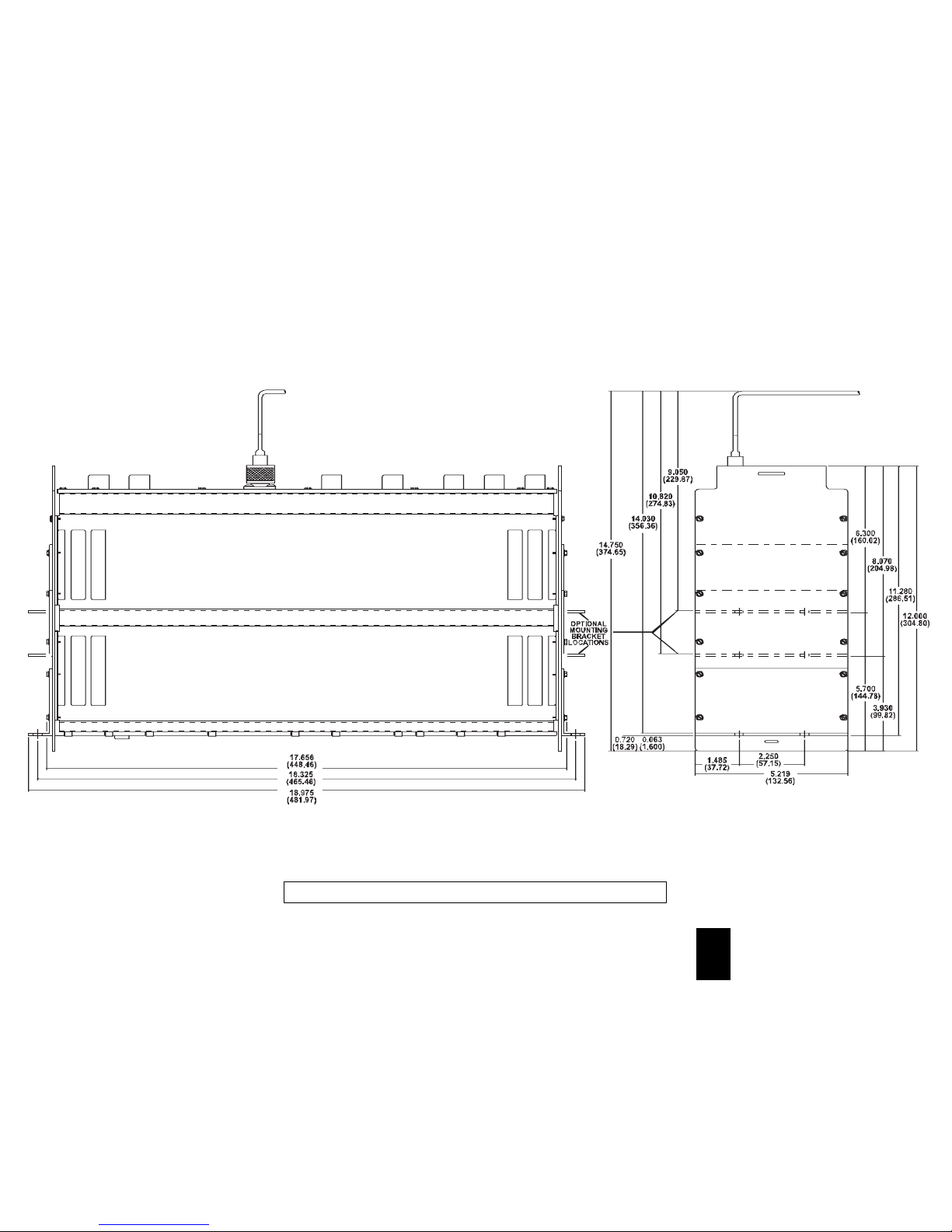
3
Figure 3–3. TCF-10B Mechanical Outline Drawing (1354D48).
Page 66

Figure 3–4. TCF-10B Connection Drawing and Jumper Options.
TCFñ10B CHASSIS CONNECTIONS
(Shows which terminals are wired for different catalog number options.)
4-WIRE
TRANSMITTER
(UHF)
TB7
J13
TB6
RS-232 FEMALE
NON-FUNCTIONAL
FOR FUTURE USE
TB5
TB2
TB1
+
+
+
TRIP 2 (TRIP +) OR UNBLOCK
SPARE
–
–
GUARD (TRIP –)
LOW SIGNAL OR LOW LEVEL
CHECKBACK TRIP
D.C. INPUT
D.C. FAIL
ALARM
SPARE
CHASSIS GROUND
RCVR.
MIC
COMMON
ALARM C.O.
ALARM C.O.
SIG. IN
1
2
3
4
5
6
7
8
9
1
2
3
4
5
6
7
8
9
1
2
3
4
5
6
7
8
9
1
2
3
4
5
6
1
2
3
4
5
6
(REAR VIEW)
J1
J2
EX CLI
0-100 µA
SPARE
LOW SIGNAL
CONTACT
NOISE
INTERNAL
JUMPER
SPARE
SPARE
3RU
MODULE
CORRESPONDING
TO TERMINAL
BLOCK
POWER
SUPPLY
E/M
OUTPUT
VOICE
ADAPTER
KEYING
10W PA
RF
INTERFACE
RECEIVER / FSK
DISCRIMINATOR
RECEIVER
LOGIC
CONTACT
CONTACT 1-1
1-2
2-1
2-2
3-1
3-2
4-1
5-1
6-1
4-2
5-2
6-2
OUTPUT
CONTACTS
OUTPUT
CONTACTS
VOICE
APPLICATIONS
VIN
TB4
TB3
1
2
3
4
5
6
1
2
3
4
5
6
DTT KEY
DTT RET.
PWR BOOST (PCR) /52b (DCR)
PWR OFF
UB/PC KEY
KEY COMMON
XMTR ON
CONTACT
SHIFT HI
CONTACT
SHIFT LO
CONTACT
7
8
9
7
8
9
NOT USED
FOR SPECIAL TTU
USE ONLY. REFER
TO FIG. 18-6
4-WIRE RECEIVE
(BNC)
4-WIRE
TRANSMIT
J1 and J2 coaxial connectors may be wired out to terminal blocks or connected to RF
hybrids. J1 is the 4-wire transmitter output. J2 is used for the 4-wire receive input only.
These terminals do not need to be wired out.
In applications where 20 VDC is required and is not supplied from the interfacing relay,an
auxiliary power supply (style 1610C07G0_) can be supplied. It mounts on the back of the
chassis. (See Fig. 3-1)
Only on sets with Electro-Mechanical outputs.
When Ju2, on the keying module, is in the DCR position, this input is used for 52b keying.
When JU2 is in the PCR position, this input is used for power boost.
NOTES:
UHF
CONNECTOR
*
BNC
CONNECTOR
*
TB6 (1-9); TB5 (7-9)
(See above)
(Combine options from above)
Module Options
Chassis Options
1. None (basic transmitter)
Transmitter Only
Receiver Only
Transceiver
(Transmitter and Receiver)
2. Voice adapter
2. Voice adapter
3. E/M outputs
1. None (basic transmitter)
TB4 (1-6), TB7 (1, 2, 6), TB3 (1-6), TB7 (3, 4)
TB1 (1-5, 8), TB7 (1, 2, 6), TB2 (1, 2, 5, 6), TB7 (3, 4)
TB1 (1-6, 8), TB7 (1, 2, 6)
TB5 (1-6)
Terminal Blocks Used
Page 67

Copyright © 2004 Pulsar Technologies, Inc.
Chapter 4. Test Equipment
4
!
CAUTION
WE RECOMMEND THAT THE USER OF THIS EQUIPMENT BECOME THOROUGHLY ACQUAINTED WITH
THE INFORMATION IN THESE INSTRUCTIONS BEFORE ENERGIZING THE TCF–10B AND ASSOCIATED
ASSEMBLIES. YOU SHOULD NOT REMOVE OR INSERT PRINTED CIRCUIT MODULES WHILE THE
TCF–10B IS ENERGIZED. ALL INTEGRATED CIRCUITS USED ON THE MODULES ARE SENSITIVE TO AND
CAN BE DAMAGED BY THE DISCHARGE OF STATIC ELECTRICITY. YOU SHOULD ALWAYS OBSERVE
ELECTROSTATIC DISCHARGE PRECAUTIONS WHEN HANDLING MODULES OR INDIVIDUAL COMPONENTS. FAILURE TO OBSERVE THESE PRECAUTIONS CAN RESULT IN COMPONENT DAMAGE.
Equipment Application
Table 4–1. Recommended Test Equipment.
High-Impedance Selective Level Meter, 380 Hz to 1 MHz
(Rycom 6021A)
1
Impedance Matching
Transmitter Power Adjustment
Receiver Margin Setting
Current Meter (Simpson 260)
1
Check dc Supply
Non-Inductive Resistor, 50Ω, 25 W (Pacific)
1
Signal Generator (H/P 3325A, Signal Crafter Model 90)
1,2
Extender Board (1353D70G01)
Transmitter Termination
General ac output for lab measurements
(See Figure 4-1.)
Reflected Power Meter, Auto VLF Power SWR Meter
(Signal Crafter 70)
1
Impedance Matching at Carrier Output
Oscilloscope (Tektronix)
1,2
Transmitter Power
Adjustment for Optional Voice Adapter
Module
Frequency Counter, 80 MHz (H/P5381A)
1,2
Transmitter Frequency
Table 4-1 shows the equipment you should use to perform the Acceptance Tests (Chapter 5) and Routine
Adjustments (Chapter 6).
1
Indicates “or equivalent” of the recommended equipment item.
2
Required only for the design verification test in Chapter 7.
Page 68

Page 4–2 December 2004
TCF–10B System Manual
Te chnologies, Inc.
Figure 4–1. Extender Board.
Page 69

Copyright © 2004 Pulsar Technologies, Inc.
Chapter 5. Installation/Adjustment Procedures
5
•Verifying initial TCF–10B factory adjustments.
• Adapting the TCF–10B to your application.
• Setting the TCF–10B operating frequencies.
• Periodic maintenance.
You perform routine adjustments in
the field for the following purposes:
• Review the Test Equipment (Chapter 4).
• Review the Adjustment Data Sheets (at the end of this
chapter); you should complete the data sheets as you
perform the Adjustment Steps.
• Review the TCF–10B Block Diagram as described
under Signal Path (Chapter 6).
• Remove the cover from the front of the chassis. After
removing the cover, set it in a safe place.
To prepare the TCF–10B for the
routine adjustment tests, perform the
following:
1. Select the TCF–10B Center Frequency.
2. Review the Adjustment Data Sheets (at the end of this
chapter); you should complete the data sheets as you
perform the Adjustment Steps.
3. Select the TCF–10B Keying Conditions.
4. Select the TCF–10B Receiver Logic.
5. Select the TCF–10B Transmitter RF Output Impedance.
6. Check the Line Tuning and Matching Equipment.
7. Check the TCF–10B Transmitter Power Levels and
Frequency.
8. Set the TCF–10B margin and Internal and External CLI
Settings.
9. Check the TCF–10B Receiver Margin.
Be sure to run the adjustment tests in
the following order:
Page 70

Page 5–2 December 2004
TCF–10B System Manual
Te chnologies, Inc.
If you are using the optional Alarm Relay, set
jumper JU1 on the Power Supply Module.
Connect the system in accordance with the
connection diagram(s), at end of the Installation
section.
5.1 Select TCF–10B Center
Frequency and Shift
5.1.1 Transmitter Operating Frequencies
If the Transmitter Module is supplied with the
TCF–10B set, remove it from the TCF–10B
chassis and select the operating frequencies.
1. Using the module extractors, remove the
Transmitter Module.
2. Select the Transmitter center frequency
(between 30 and 535 kHz) by turning the four
Transmitter rotary programming switches (in
0.1 kHz steps) with a small screwdriver until
the desired frequency appears in the (four)
windows of the Transmitter Control Panel.
3. Set switch S5 for the appropriate frequency
shift, as shown in the following table.
4. Insert the module back into the TCF–10B
chassis by seating it with firm pressure.
5.1.2 Receiver Center Frequency
If a Receiver Module is supplied with the
TCF–10B set, power up the TC-10B unit with the
appropriate dc power. With a small screwdriver,
depress the “SET” button on the front of the
receiver module. The frequency display will begin
to flash. Depress the raise or lower button until the
desired frequency is displayed. Depress “SET”
again to select this frequency. If you are not ready
to set the sensitivity, depress the “CANCEL”
button. If you are ready to set the sensitivity,
depress the “SET” button and proceed with the
steps listed in Section 5.7.
Frequency Shift
Settings
Narrow Band, Up Dwn Up Up 100 Hz
Narrow Shift
Wide Band, Up Dwn Up Up 100 Hz
Narrow Shift
Wide Band, Dwn Up Dwn Up 250 Hz
Wide Shift
Extra Wide Band, Up Dwn Up Dwn 500 Hz
Wide Shift
Position Settings
1 2 3 4
Shift
!
CAUTION
MAKE SURE THAT THE POWER HAS BEEN
TURNED “OFF” USING THE POWER SWITCH
(S1) ON THE POWER SUPPLY MODULE; THE
INPUT (D3) AND OUTPUT (D11) LEDS SHOULD
NOT SHOW RED LIGHTS.
Page 71

5.2 Select TCF–10B Keying
Conditions
5.2.1 Test Switches
Three push-button switches are provided for test
purposes:
S1 High-Level Power (HL)
S2 Shift High (SH)
S3 Shift Low (SL)
Each push-button is recessed, and can be activated
by sliding an object (e.g., a pen or pencil) through
each push-button access location on the Keying
Module front panel.
5.2.2 Keying Module LEDs
The LEDs at the bottom of the Keying Module
front panel indicate the Keying condition:
HL High-Level Key Output
SL Shift High Key Output
SH Shift Low Key Output
VVoice-Level Key Output
TX Any Transmitter Key Output
5.2.3 Keying Module Jumpers
Remove the Keying Module from the chassis and
set jumpers (JU1 thru JU14) as desired.
JU1 Allows you to select between the
NORM/INVERT positions for Power
Off. Select the normal (NORM)
position to allow a Keying function in
the transmitter when proper voltage
level (15V, 48V, 125V, 250V) is
applied to the input terminals. Select
the invert (INV) position to allow a
Keying function in the Transmitter
when voltage is not present at the
input terminals. Set JU1 to invert
(INV).
JU2 Selects between a Directional
Comparison system and Phase
Comparison system. Set JU2 to DCR
(Directional Comparison).
JU3 This link allows you to select between
a 1W (Guard)/10W (Trip) or 10W
(Guard)/10W (Trip) operation by
placing the link in the 1/10W or
10/10W position, respectively. Select
the 1W/10W position.
JU4 Selecting the 2-frequency (2F)
position will set the Keying Module as
a two-frequency system. Selecting the
three-frequency (3F) position will set
the Keying Module in mode to
correctly operate as a three-frequency
system. Select the 3F position.
JU6 Placing JU6 to the IN position
activates the shift high contact; the
OUT position deactivates the shift
high contact.*
JU7 Placing JU7 to the IN position
activates shift low contact; the OUT
position deactivates shift low contact.*
JU8 Places shift high contacts in either the
normally open (NO) position or the
normally closed (NC) position.
JU9 Places shift low contacts in either the
normally open (NO) position or the
normally closed (NC) position.
JU10–
JU14 Provides input keying voltage selec-
tions: 15/20V, 48V, 125V, 250V.
After setting the jumpers, insert the Keying
Module back into the TCF–10B chassis.
5.3 Select TCF–10B Receiver
Logic
Set the Receiver Logic PC Board switches (see
Section 15.3) in accordance with the TCF–10B
application:
• 2-Frequency, Directional Comparison
• 2-Frequency, Phase Comparison
• 3-Frequency, Directional Comparison
December 2004 Page 5–3
Chapter 5. Installation/Adjustment Procedures
5
*Place in the “OUT” position when using with the Phase
Comparison relay systems.
Page 72

5.4 Select TCF–10B Transmitter
RF Output Impedance
1. Configure the RF Output Impedance.
Remove the RF Interface Module from the
TCF–10B chassis and configure the output
impedance by setting jumpers:
• JU4 when set, provides 50Ω
• JU3 when set, provides 75Ω
• JU2 when set, provides 100Ω
2. Select 2- or 4-wire Receiver Input, using
jumpers JU1 and JU5:
• IN position for 2-wire (not normally used
for TCF–10B)
• OUT position for 4-wire (both JU1 and JU5
must be OUT)
3. If you are using an external hybrid chain, and
the receive signal is not high enough, a higher
sensitivity may be desirable. Set jumper JU6
to HIGH, if necessary.
4. Insert the RF Interface Module back into the
TCF–10B chassis.
5.5 Check Line Tuning and
Matching Equipment
1. Refer to the appropriate instructions for line
tuning equipment.
2. Perform the required adjustments.
5.6 Check TCF–10B Transmitter
Power Levels and
Frequency
Turn “ON” the power and check the dc voltage
outputs from the Power Supply Module. Then,
turn “OFF” the power and remove the coaxial
cable connection to the Line Tuner and substitute
a 50, 75, or non-inductive 100Ω resistor termination (in accordance with the jumper settings in
5.4-1).
5.6.1 Check High-Level Output
1. Connect the Selective Level Meter to the 10W
PA Module control panel, at test jacks:
TJ1 Input - Top Jack
TJ2 Common - Bottom Jack
2. Tune the meter to the Transmitter frequency.
3. Turn power “ON” at the Power Supply
Module.
4. On the Keying Module control panel, press
and hold the top push-button (marked HL) to
key the Transmitter at High Level power.
The “HL” and “TX” LEDs should show
red.
5. Record the Selective Level Meter reading (at
TJ1, TJ2). The meter should measure .224
Vrms (0 dBm at 50Ω reference) for full High-
Level keying (10W power). If you measure 0
dBm, skip ahead to Step 8.
6. If the meter does not measure 0 dBm, turn the
power “OFF” at the Power Supply Module
and remove the Transmitter Module from the
chassis. Place the extender board into the
Transmitter Module position of the chassis.
Then plug the Transmitter Module onto the
extender board.
Page 5–4 December 2004
TCF–10B System Manual
Te chnologies, Inc.
!
CAUTION
DO NOT ALLOW INEXPERIENCED PERSONNEL
TO MAKE THESE ADJUSTMENTS. PERSONNEL
MUST BE COMPLETELY FAMILIAR WITH THE
HAZARDS INVOLVED.
Page 73

7. Turn the Power Supply “ON”. Turn the 10W
Adjust potentiometer R13 on the Transmitter
Module until the Selective Level Meter (at the
10W PA TJ1, TJ2) reads .224Vrms (0 dBm at
50Ω reference). Then place the Transmitter
Module back in the chassis.
If it is desirable to set full power at less than
10W, turn the 10W adjust potentiometer
(R13) accordingly. The level at the RF
Interface Module (TJ1, TJ2) is 40 dB higher
than at the 10W PA Module (TJ1, TJ2).
For example: If 22 dBm is desired at RF
Interface(TJ1, TJ2), set potentiometer R13 so
that 10W PA (TJ1, TJ2) reads -18 dBm. (The
PA gain is adjustable with R53 on the 10W PA
Module.)
8. Monitor the output of the 10W PA Module at
the RF Interface Module test jacks TJ1
(Line)/TJ2 (Line Common). On the 10W PA
Module, adjust potentiometer R53 INPUT
LEVEL SET for 22.4Vrms (10W) output
level.
9. On the Keying Module control panel, release
the (HL) push-button to reduce the
Transmitter power.
The “HL” LED should not be red; but the
“TX” LED should remain red.
5.6.2 Check Low-Level Output
1. With the conditions the same as for the HighLevel Output check:
• Selective Level Meter at the 10W PA
Module control panel (TJ1, TJ2)
• Meter tuned to XMTR frequency
• Power “ON”
The “TX” LED should show red.
2. With the Transmitter keyed on LL, record the
Selective Level Meter reading (at TJ1, TJ2).
The meter should measure .0707Vrms (-10
dBm at 50Ω reference) for Low-Level keying
(1W power).
3. If the meter does not measure -10 dBm, turn
the power “OFF” at the Power Supply Module
and remove the Transmitter Module from the
chassis. Place the extender board into the
Transmitter Module position of the chassis.
Then plug the Transmitter Module onto the
extender board.
4. Turn the 1W Adjust potentiometer (R12) on
the Transmitter Module until the Selective
Level Meter (at the 10W PA TJ1, TJ2) reads
.0707Vrms (-10 dBm at 50Ω reference).
5. Repeat step 5.6.1-8 (above) at 7.07Vrms (1W)
output level.
6. Turn “OFF” the power supply.
7. Place the Transmitter Module back in the
chassis.
We recommend that you set the low level power
10 dB below full power. You may, however, use
any power level between 10W and 50mV.
|| 5.6.3 Adjusting Low-Level Output
for a Level Other Than 1W
Should you wish to adjust the low-level output for
a level other than 1W, use R12 on the transmitter
card to adjust to the level you desire. The
following chart gives you several levels that you
may use for reference.
For a 10W low-level output, it is easier to move
jumper JU3 on the keying module to the 10/10W
position.
||
5.6.4 Check Voice-Level Output
Perform this procedure only if you are using the
Voice Level Output option.
December 2004 Page 5–5
Chapter 5. Installation/Adjustment Procedures
5
Desired Power Output
(Watts)
Reading at 10W
PA TJ1, TJ2 (V rms)
0.5 0.05
1.5 0.0866
2.0 0.10
2.5 0.112
5 0.158
10 See Note
Page 74

1. With the conditions the same as for the HighLevel Output check:
• Selective Level Meter at the 10W PA
Module control panel (TJ1, TJ2)
• Meter tuned to XMTR frequency
• Power “ON”
2. Key the carrier set by lifting the handset from
its cradle, while muting the microphone, to
key the Transmitter at Voice-Level (4.3W
power, when the High-Level power is set to
10W).
The “V” and “TX” LEDs should show red.
3. Record the Selective Level Meter reading (at
TJ1, TJ2). The meter should measure .148
Vrms (-3.6 dBm at 50Ω reference) for Voice
Keying. If you measure -3.6 dBm, skip ahead
to Step 6.
4. If the meter does not measure -3.6 dBm, turn
the power “OFF” at the Power Supply Module
and remove the Transmitter Module from the
chassis. Place the extender board into the
Transmitter Module position of the chassis.
Then plug the Transmitter Module onto the
extender board.
5. Turn the Voice Carrier Adjust potentiometer
(R14) on the Transmitter Module until the
Selective Level Meter (TJ1, TJ2) reads .148
Vrms (-3.6 dBm at 50Ω reference). Then
place the Transmitter back in the chassis.
If using a full power level (other than 10W),
you should set the VF level accordingly, i.e.,
3.6 dB below the high-level value.
6. Monitor the output of the carrier set with an
oscilloscope at the 10W PA Module test jacks:
• TJ1
• TJ2
7. Voice key the Transmitter by lifting the
handset from its cradle and by whistling
loudly (about 1 kHz) to achieve the following
voltages:
•~.62V p-p (overall)
•~.20V p-p (valley)
8. If the voltages above (.62/.20) do not approximate a ratio value of 3, adjust the AM
Modulation Adjust potentiometer (R11) on
the Transmitter, as follows:
• Clockwise if not enough signal (a value
less than 3).
• Counterclockwise if too much signal (a
value significantly greater than 3).
9. Un-key the Push-to-Talk switch (or handset).
5.6.5 Check Transmitter Frequency
1. At the Keying Module, push the recessed
push-button “SH” to shift the frequency
higher: (f
C
= center freq. set on front of
module)
f
C
+ 100 Hz Narrow Band or Wide Band,
Narrow Shift
f
C
+ 250 Hz Wide Band, Wide Shift
f
C
+ 500 Hz Extra Wideband, Wide Shift
If the frequency shift is incorrect on the
Transmitter Module, check the position of switch
S5 for the correct amount of shift.
2. At the Keying Module, release the “SH” pushbutton and push the “SL” push-button to shift
the frequency lower:
f
C
– 100 Hz Narrow Band or Wide Band,
Narrow Shift
f
C
– 250 Hz Wide Band, Wide Shift
f
C
– 500 Hz Extra Wideband, Wide Shift
If the frequency is incorrect on the Transmitter
Module, check the position of switch S5 for the
correct frequency. Release push-button “SL”.
Page 5–6 December 2004
TCF–10B System Manual
Te chnologies, Inc.
Page 75

5.6.6 Restore Transmitter Module to
Normal
1. Turn the power “OFF” at the Power Supply
Module.
2. Remove the 50, 75, or 100Ω resistor termina-
tion and replace the coaxial cable connection
to the Line Tuner.
3. Move the Selective Level Meter to test jacks
marked “LINE” (on the RF Interface control
panel):
• TJ1 (Line)
• TJ2 (Common)
4. Turn the power “ON” at the Power Supply
Module.
5. On the RF Interface Module, configure output
impedance by setting a jumper. The Selective
Level Meter (TJ1, TJ2) should show a
maximum reading (Vrms) for 1W (+30 dBm)
power, as follows:
JU4 When set, provides 50Ω (7.07Vrms)
JU3 When set, provides 75Ω (8.6Vrms)
JU2 When set, provides 100Ω (10.0Vrms)
6. If the above (Vrms) values are not achieved,
recheck the tuning of the coupling system, as
it is not presenting the Transmitter with the
proper termination.
5.7 Check TCF–10B Receiver
Margin Setting using
Remote Carrier Signal
1. At the Power Supply Module, turn the power
“ON”. If the frequency is not already set, refer
to section 5.1.2.
2. Arrange for a received signal from the remote
end,
3. Sensitivity setting:
On the Receiver module to complete the setting:
a) Hit “SET” twice until the display reads
“SET SENS?”
b) With the remote signal being received (at
the remote end, push the “LL button on the
keying module), depress “SET” again.
c) If you’re not adjusting the 15 dB margin,
depress “SET” again. If you are, then
depress “RAISE” or “LOWER” as
required to adjust it up or down 5 dB.
d) If you are not going to adjust an external
carrier level meter, depress “SET”.
Otherwise, press “RAISE” or “LOWER”
as required.
4. Set the external CLI.
Once you have completed the sensitivity
setting, the display scrolls this message: "Set
Ext CLI? – Hit Raise/Lower or Set when
done...”
To calibrate the external CLI push the
CANCEL/RAISE or LOWER button. The
external CLI meter will move up and down
accordingly. The external meter is a 100µA
instrument. If it is calibrated in µA, the meter
should be set to read 67µA (this is equivalent
to 0 dB on the internal meter). The setting
should vary 3.3µA for each dB the margin
adjustment has been raised or lowered from
the 15 dB margin. If the meter is calibrated in
December 2004 Page 5–7
Chapter 5. Installation/Adjustment Procedures
5
NOTES:
1. The foregoing procedure adjusts the
Receiver margin to the recommended 15 dB
value.
2. The Receiver bar graph CLI meter reading
should be 0 dB at this time.
3. In three-terminal line applications, the margin
adjustment procedure should use the weaker
of the two received signals.
4. When applying the TCF–10B with a phase
comparison relay, do not readjust the
Receiver level when keying with a square
wave signal. The CLI will read around -10 dB,
but this is an average reading of the on and
off square wave. The receiver will still
maintain the 15 dB margin. The CLI reading is
only accurate for a non-amplitude modulated
signal.
Page 76

dB, set the meter to read equal to the internal CLI meter.
To accept the displayed level, push the SET button.
This completes the Receiver setting procedure.
5.8 Prepare the TCF–10B for Operation
Be sure that power is “ON” at the Power Supply Module.
1. Restore the Keying Module to the desired settings. (See the TCF–10B Adjustment Data Sheet near the
end of this chapter. This data sheet is to be completed by your settings department.)
2. Replace the cover on the TCF–10B control panel.
a) Secure the latch by pushing inward and sideways until the cover is secure.
b) You may lock the latches into place using meter seals.
This completes the “Routine Adjustment” procedure. The TCF–10B is ready to be put into operation.
Page 5–8 December 2004
TCF–10B System Manual
Te chnologies, Inc.
NOTE
When placing the TCF–10B into service,
refer to the manual for the relay system you
are using with the TCF–10B System.
Page 77

TCF–10B ADJUSTMENT DATA SHEET
(1) Power Supply Test Jack
+20 Vdc . . . . . . . . . . . . . . . . . . . . . . . . . . . . . . . . .(+20V/Comm)
—20 Vdc . . . . . . . . . . . . . . . . . . . . . . . . . . . . . . . . . (—20V/Comm)
Input & Output LEDs ON . . . . . . . . . . . . . . . . . .
(2) 10W PA
Voice PA IN . . . . . . . . . . . . . . . . . . . . . . . . . . . .(Input/Common)
LLPA IN . . . . . . . . . . . . . . . . . . . . . . . . . . . . . . .(Input/Common)
HLPA IN . . . . . . . . . . . . . . . . . . . . . . . . . . . . . . .(Input/Common)
Transmit LED ON . . . . . . . . . . . . . . . . . . . . . . . . ——
(3) RF Interface
XMTR Frequency, Shift High . . . . . . . . . . . . . . . .(Line/Line Com)
XMTR Frequency, Shift Low . . . . . . . . . . . . . . . .(Line/Line Com)
XMTR Frequency, Center Freq. . . . . . . . . . . . . . .(Line/Line Com)
Voice Level (if using a voice adapter) . . . . . . . . . .(Line/Line Com)
LL Level (guard) . . . . . . . . . . . . . . . . . . . . . . . . . .(Line/Line Com)
HL Level . . . . . . . . . . . . . . . . . . . . . . . . . . . . . . . .(Line/Line Com)
Received Frequency, Shift High . . . . . . . . . . . . . .(RCVR/RCVR Com)
Received Frequency, Shift Low . . . . . . . . . . . . . .(RCVR/RCVR Com)
Received Frequency, Center Freq. . . . . . . . . . . .(RCVR/RCVR Com)
Received Level . . . . . . . . . . . . . . . . . . . . . . . . . .(RCVR/RCVR Com)
Received Noise Level, w/Rem Transmitter off . . .(RCVR/RCVR Com)
(note bandwidth of meter when measuring noise level)
December 2004 Page 5–9
Chapter 5. Installation/Adjustment Procedures
5
Page 78

Page 5–10 December 2004
TCF–10B System Manual
Te chnologies, Inc.
(4) Receiver/Discriminator (from other end)
bar graph meter w/LL Keyed . . . . . . . . . . . . . . .(dB)
bar graph meter w/HL Keyed . . . . . . . . . . . . . . .(dB)
Noise LED Not Lit . . . . . . . . . . . . . . . . . . . . . . . . —
Low-Level LED Not Lit . . . . . . . . . . . . . . . . . . . . —
(5) Receiver Logic
(a) 2 Frequency . . . . . . . . . . . . . . . . . . . . . . . . . . . .
Good Channel LED . . . . . . . . . . . . . . . . . . . . . . .
Checkback Trip LED . . . . . . . . . . . . . . . . . . . . . .
Trip LED . . . . . . . . . . . . . . . . . . . . . . . . . . . . . . .
Guard LED . . . . . . . . . . . . . . . . . . . . . . . . . . . . . .
(b) 3 Frequency Logic
Good Channel LED . . . . . . . . . . . . . . . . . . . . . . .
Checkback Trip LED . . . . . . . . . . . . . . . . . . . . . .
UB/POTT Trip LED . . . . . . . . . . . . . . . . . . . .
DTT Trip LED . . . . . . . . . . . . . . . . . . . . . . . .
Guard LED . . . . . . . . . . . . . . . . . . . . . . . . . . . . . .
(c) Phase Comparison
Good Channel LED . . . . . . . . . . . . . . . . . . . . . . .
Trip Positive LED . . . . . . . . . . . . . . . . . . . . . . . . .
Trip Negative LED . . . . . . . . . . . . . . . . . . . . . . . .
(6) Rear of Chassis
Reflected Power . . . . . . . . . . . . . . . . . . . . . . . . .(J1) (%)
Test Performed By _______________________________ Date ________________
Page 79

December 2004 Page 5–11
Chapter 5. Installation/Adjustment Procedures
5
TCF–10B JUMPER & SWITCH SETTINGS
(1) POWER SUPPLY
JU1 Power Alarm NO U NC U
(2) KEYING
JU1 Power On/Off NORM U INV U
JU2 Directional Comparison/ DCR U PC U
Phase Comparison
JU3 1W Guard, 10W Trip or 1 W/10 W
U 10 W/10 W U
10W Guard — 10W/Trip
JU4 2-Frequency or 3-Frequency 2F
U 3F U
JU6 Shift High Contacts IN U OUT U
JU7 Shift Low Contacts IN U OUT U
JU8 NO or NC for Shift High NO U NC U
JU9 NO or NC for Shift Low NO U NC U
JU10 DTT Keying Voltage 15V U 48V U 125V U 250V U
JU11 Ext. Voice Keying Logic 15V U 48V U 125V U 250V U
JU12 PWR Boost/52b Keying 15V U 48V U 125V U 250V U
Voltage
JU13 Power Off Keying Voltage 15V
U 48V U 125V U 250V U
JU14 UB, POTT, PC Keying 15V U 48V U 125V U 250V U
Voltage
Page 80

Page 5–12 December 2004
TCF–10B System Manual
Te chnologies, Inc.
(3) TRANSMITTER
S5 Frequency—Shift Select (Down = Selected)
Position Up Down
1 (50 Hz)
2 (100 Hz)
3 (200 Hz)
4 (400 Hz)
(4) 10W POWER AMPLIFIER
JU1 Power Monitor NO U NC U
(5) RF INTERFACE
JU1 2-Wire/4-Wire (2-wire) IN U (4-wire) OUT U
JU2 Impedance-100Ω IN U OUT U
JU3 Impedance- 75Ω IN U OUT U
JU4 Impedance- 50Ω IN U OUT U
JU5 2-Wire/4-Wire (2-wire) IN U (4-wire) OUT U
JU6 Sensitivity HIGH U NORM U
(6) RECEIVER MODULE
FSK Receiver (TCF-10B):
Dip Switch (SW 1) OPEN (Down or Off) Closed (Up or On)
Pos 1 X FSK T ON/OFF
Pos 2
T No voice T Voice
Pos 3 T DTT 2F T 3F or UB 2F
Pos 4
T DCR T PCR
Pos 5 T Shift down to trip T Shift up to trip*
FSK Bandwidth Shift 2F/3F Pos 6 Pos 7 Pos 8
T 300 100 2F OFF OFF OFF
T 600 250 2F OFF OFF ON
T 1200 500 2F OFF ON OFF
T 600 250 3F OFF ON ON
T 1200 500 3F ON OFF OFF
T 600 100 2F ON OFF ON
T 1200 250 2F ON ON OFF
JU3 !Low Signal Contact T NO T NC
||
|| *2F Only
|| ! = Inverted
Page 81

December 2004 Page 5–13
Chapter 5. Installation/Adjustment Procedures
5
(7) RECEIVER LOGIC - for information on the settings, please see Chapter 16
CF20-RXLMN-004: 2-FREQUENCY DIRECTIONAL COMPARISON LOGIC
Page 82
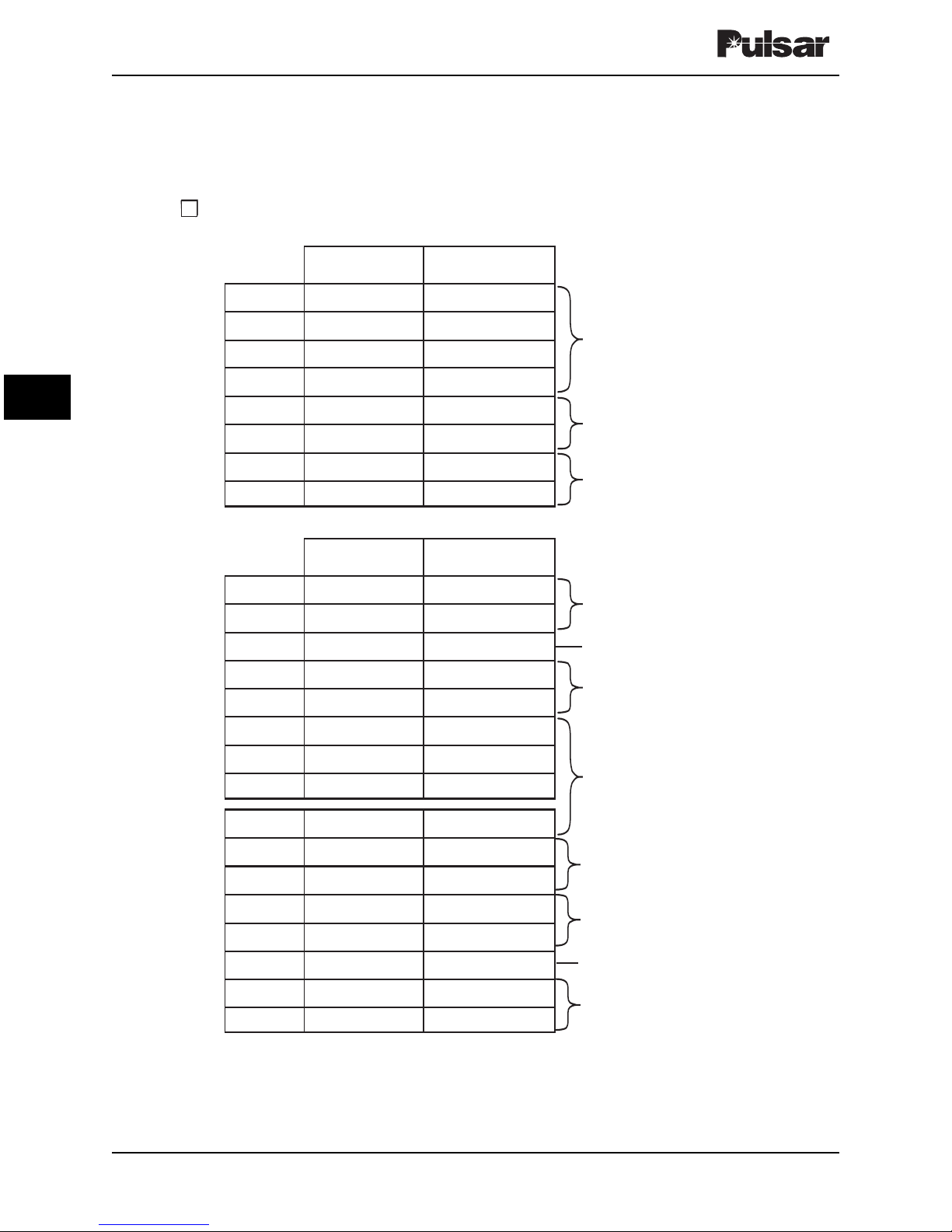
Page 5–14 December 2004
TCF–10B System Manual
Te chnologies, Inc.
SW1–1
SW1–2
SW1–3
SW1–4
SW1–5
SW1–6
SW1–7
SW1–8
UB/POTT
TRIP DELAY
TRIP HOLD
GUARD HOLD
SW2–1
SW2–2
SW2–3
SW2–4
SW2–5
SW2–6
SW2–7
SW2–8
UNBLOCK TIME
GUARD BEFORE TRIP
OPTIONS
DTT
TRIP DELAY
NOISE ALLOWS UB TRIP
TRIP HOLD
GUARD HOLD
SW3–1
SW3–2
SW3–3
SW3–4
SW3–5
SW3–6
SW3–7
SW3–8
LOW LEVEL DELAY
CHECKBACK #1 or #2
OPEN (OFF) CLOSED (ON)
OPEN (OFF) CLOSED (ON)
CF20–RXLMN–002: 3-FREQUENCY DIRECTIONAL COMPARISON LOGIC
Page 83

December 2004 Page 5–15
Chapter 5. Installation/Adjustment Procedures
5
(8) VOICE ADAPTER
JMP1 U NO U NC
SW1 (Function active when in “ON” position)
POS 1 - Front Panel push-button gives alarms at opposite end TCF-10B
POS 2 - Carrier Alarm (TC-10B)
POS 3 - Push to talk function (TC-10B)
POS 4 - Beeper enabled (Both)
(9) EM (RELAY) OUTPUT
JU1 Relay 1 Driver Trip 1 (DTT for 3F) U Trip 2 (UB/POTT, 3F) U Guard U
JU2 Relay 2 Driver Trip 1 (DTT for 3F) U Trip 2 (UB/POTT, 3F) U Guard U
JU3 Relay 3 Driver Trip 1 (DTT for 3F) U Trip 2 (UB/POTT, 3F) U Guard U
JU4 Relay 4 Driver Trip 1 (DTT for 3F) U Trip 2 (UB/POTT, 3F) U Guard U
JU5 Relay 5 Driver Trip 1 (DTT for 3F) U Trip 2 (UB/POTT, 3F) U Guard U
JU6 Relay 6 Driver Trip 1 (DTT for 3F) U Trip 2 (UB/POTT, 3F) U Guard U
JU7 Relay 1 Contact NO U NC U
JU8 Relay 2 Contact NO U NC U
JU9 Relay 3 Contact NO U NC U
JU10 Relay 4 Contact NO U NC U
JU11 Relay 5 Contact NO U NC U
JU12 Relay 6 Contact NO U NC U
*JU13 Trip Delay _______________________________________
*JU14 Trip Delay _______________________________________
*
On 1606C53G02 only
Page 84
Page 5–16 December 2004
TCF–10B System Manual
Te chnologies, Inc.
Technologies, Inc.
USER NOTES
Page 85

6.1 Power Supply Module
Terminal Block (TB7)
TB7/1 Positive Vdc (also pins C/A-12)
TB7/2 Negative Vdc (also pins C/A-14)
The Vdc is received from three (3) available
groups of station batteries:
• 38–70 Vdc (48 or 60 Vdc nominal)
• 88–140 Vdc (110 or 125 Vdc nominal)
• 176–280 Vdc (220 or 250 Vdc nominal)
TB7/3 Failure Alarm Signal (also pins
C/A-16)
TB7/4 Failure Alarm Signal (also pins
C/A-18)
TB7/5 Spare
TB7/6 Chassis Ground
Voltage Output to All Other Modules
Positive voltage outputs (+20 Vdc) are
available at pins A-2 and A-4, while negative
voltage outputs (-20 Vdc) are available at pins
C-2 and C-4. Common to ground (pins C/A30 and C/A-32).
Optional low-voltage power alarm relay
outputs
Optional low-voltage power alarm relay
outputs are available at pins C/A-16 and
C/A-18.
6.2 Keying Module
Voltage Inputs
+20 Vdc Pins A-2 and A-4
-20 Vdc Pins C-2 and C-4
Common Pins C/A-30 and C/A-32
Terminal Block (TB4)
TB4/1 DTT (Direct Transfer Trip) Key (to
pin A-10)
TB4/2 DTT Return (to pin C-10)
TB4/3 52b or Pwr Boost (to pin C-16)
TB4/4 Pwr Off (to pin A-16)
TB4/5 UB (Unblock)/PC (Phase Com-
parison) Key (to pin A-22)
TB4/6 Key Common return for Power
Boost, Power Off, and UB/PC key
(to pin C-22)
Inputs
• External Voice Key (pins C/A-12)
• Optional Voice Key (pin C-24)
Outputs to Transmitter Module
• Shift Low (pin A-28)
• Shift High (pin A-26)
• High-Level 10W Key (pin A-8)
•Voice Key (pin A-6)
• Any Transmitter Key (pin C-6)
The following description of the TCF–10B signal path is in accordance with the Functional Block
Diagram (see Figure 6-1), and the rear panel previously shown (in Figure 3-1). The discussion of signal
path may be useful during Design Verification Testing (Chapter 7) or Installation/Adjustment (Chapter 5).
Copyright © 2004 Pulsar Technologies, Inc.
Chapter 6. Signal Path
6
Page 86

Outputs to 10W PA Module
• Contact Shift Low (pins C/A-20)
• Contact Shift High (pins C/A-14)
Output to Receiver Module
Any Transmitter Key (pin C-6)
6.3 Transmitter Module
Voltage Inputs
+20 Vdc Pins A-2 and A-4
-20 Vdc Pins C-2 and C-4
Common Pins C/A-30 and C/A-32
Inputs from Keying Module (4V Standby,
19V Keyed)
• Shift Low (pins C/A-24)
• Shift High (pin C-10)
• High-Level (10W) Key (pins C/A-8)
•Voice Key (pins C/A-6)
• Any Transmitter Key (pin A-10)
Input from Optional Voice Adapter Module
AM Voice (pin C/A-26)
Output to 10W PA Module
0 dBm for 10W or -10 dBm for 1W
Transmitter output power (pins C/A-28)
6.4 10W PA Module
Voltage Inputs
+20 Vdc Pins A-2 and A-4
-20 Vdc Pins C-2 and C-4
Common Pins C/A-30 and C/A-32
Terminal Block (TB3)
TB3/1 TX (Transmitter) ON (pins C/A-12)
TB3/2 TX (Transmitter) ON (pins C/A-14)
TB3/3 Contact 1 Shift High, to alarms
TB3/4 Contact 2 Shift High, to alarms
TB3/5 Contact 1 Shift Low, to alarms
TB3/6 Contact 2 Shift Low, to alarms
Input from Transmitter Module
0 dBm for 10W output or -10 dBm for 1W
output (pins C/A-28)
Output to RF Interface Module
1W, voice or 10W (pins C/A-16 and C/A-18)
6.5 RF Interface Module
Voltage Inputs
+20 Vdc Pins A-2 and A-4
-20 Vdc Pins C-2 and C-4
Common Pins C/A-30 and C/A-32
Input from 10W PA Module
1W, voice, or 10W (pins C/A-16 and C/A-18)
Output to Receiver Module
RF Output Signal (pins C/A-28)
Other Outputs
1) Cable Jacks
• J1–RF Interface module (C/A-12 and C/A-
10) Transmitter RF output line, through
coaxial cable (UHF)
• J2–RF Interface module (C/A-24 and C/A-
22) Receiver RF input line coaxial cable
(BNC)
Page 6–2 December 2004
TCF–10B System Manual
Te chnologies, Inc.
Page 87

2) Jumpers
JU1 UHF Chassis Ground (for J1, not
supplied)
JU2 BNC Chassis Ground (for J2, not
supplied)
6.6 Receiver/Discriminator
Module
Voltage Inputs
+20 Vdc Pins A-2 and A-4
-20 Vdc Pins C-2 and C-4
Common Pins C/A-30 and C/A-32
Input from Keying Module
Any Transmitter Key (pin C-6)
Input from RF Interface Module
RF Output Signal (pin C-28)
Output to Discriminator and CLI Module
20 kHz signal (pin A-28)
RF Output to Optional Voice Adapter
•20kHz signal through jumper JU4
• 5.02 MHz signal through jumper JU3
Terminal Block (TB2)
TB2/1 Optional External CLI Meter
(pins C/A-12)
TB2/2 Optional External CLI Meter
(pins C/A-14)
TB2/3 Noise + (pins C/A-16)
TB2/4 Noise - (pins C/A-18)
TB2/5 !Low Signal Contact (pins C/A-20)
TB2/6 !Low Signal Contact (pins C/A-22)
!Low Signal = Not Low Signal
Output to Receiver Logic Module
• Level (pin C-28)
• High/Low Frequency (pin A-28)
• Center Frequency (pin A-10)
• Noise (pin A-8)
6.7 Receiver Logic Module
Voltage Inputs
+20 Vdc Pins A-2 and A-4
-20 Vdc Pins C-2 and C-4
Common Pins C/A-30 and C/A-32
Input from CLI/Discriminator Module
• Level (pins C/A-26)
• High/Low Frequency (pins C/A-28)
• Center Frequency (pin C-10)
• Noise (pin C-8)
Terminal Block (TB1)
TB1/1 + V Input from pins C/A-12
TB1/2 Guard or Trip Negative from pins
C/A-14
TB1/3 Noise from pins C/A-16
TB1/4 Trip 2, Trip Positive or Unblock
from pin C-18
TB1/5 !Low Signal* or !Low Level* from
pin C-20
TB1/6 Common from pin C-22
TB1/7 Common from pin A-22
TB1/8 Checkback Trip from pin A-20
TB1/9 Unused
*! Low Signal means Not Low Signal
! Low Level means Not Low Level
Output to EM Output Module
•Trip 1/Trip 2 (pin A-24)
• Guard (pin C-24)
December 2004 Page 6–3
Chapter 6. Signal Path
6
Page 88

6.8 EM Output Module
Voltage Inputs
+20 Vdc Pins A-2 and A-4
-20 Vdc Pins C-2 and C-4
Common Pins C/A-30 and C/A-32
Input from Receiver Logic Module
•Trip 1/Trip 2 (pin C-20)
• Guard (pin A-20)
Terminal Block (TB6)
TB6/1 Contact 1-1 from pin A/C-8
TB6/2 Contact 1-2 from pin A/C-10
TB6/3 Contact 2-1 from pin A/C-12
TB6/4 Contact 2-2 from pin A/C-14
TB6/5 Contact 3-1 from pin A/C-16
TB6/6 Contact 3-2 from pin A/C-18
TB6/7 Contact 4-1 from pin C-22
TB6/8 Contact 5-1 from pin C-24
TB6/9 Contact 6-1 from pin C-26
Output to Optional Voice Adapter Module
• Contact 4-2 (pin A-22)
• Contact 5-2 (pin A-24)
• Contact 6-2 (pin A-26)
6.9 Optional Voice Adapter
Module
Voltage Inputs
+20 Vdc Pins A-2 and A-4
-20 Vdc Pins C-2 and C-4
Common Pins C/A-30 and C/A-32
RF Input from Receiver Module
•20kHz signal through jumper JU4 to pin
C/A-26
• 5.02 MHz signal through jumper JU3 to pin
C/A-26
Output to Keying Module
Voice Key (pin C/A-22)
Output to Transmitter Module
AM Voice (pin A-28)
Terminal Block TB-5
TB5/1 External receiver signal from C/A-8
TB5/2 External microphone input to
C/A-10
TB5/3 Common to A/C-12
TB5/4 Alarm contact to C/A-16
TB5/5 Alarm Contact to C/A-18
TB5/6 External signaling input to C/A-20
Page 6–4 December 2004
TCF–10B System Manual
Te chnologies, Inc.
Page 89

Figure 6-1. TCF-10B Functional Block Diagram. (CF44-VER05)
RECEIVER LOGIC OUTPUTS
TB1 2F 3F* PHASE COMP.
1 +V INPUT +V INPUT +V INPUT
2 GUARD UB/POTTGUARD TRIP—
3 NOISE NOISE NOISE
4 TRIP UB/POTTTRIP TRIP+
5 !LOW LEVEL !LOW LEVEL !LOW LEVEL
8CHECKBACK TRIP CHECKBACK TRIP —
* FOR 3F SYSTEMS, DTT TRIP & GUARD ARE AVAILABLE ON THE ELECTRO-MECHANICAL OUTPUT MODULE S TB6 & TB5
! = Inverted
Page 90

7.1 Preliminary Checks
7.1.1 Checking the Chassis
Nameplate
Verify that the proper dc supply voltage and
module options are on the chassis nameplate.
Also, check for narrow, wide, or extra wide band;
Phase Comparison or Directional Comparison (2or 3-Frequency).
Check to ensure that all required modules are
supplied and are installed in the proper chassis
slots. The slots are labeled on the top edge of the
chassis.
7.1.2 Inspecting for the Correct dc
Voltage
With the power “OFF,” remove the Power Supply
module and inspect it for the correct dc voltage, as
specified in Table 7-1.
7.2 TCF–10B Preliminary
Connections
1. Refer to the Block Diagram (see Chapter 6,
Signal Path) for keying and output connections.
2. Connect the dc supply to the appropriate
terminals on the Rear Panel (see Figures 3-1
and 3-4, in Chapter 3, Installation).
3. Terminate the Transmitter output with a non-
inductive 50Ω, 25W resistor.
4. Connect the Selective Level Meter (Rycom
6021A) across the 50Ω resistor load.
It is not intended to perform the design verification tests at installation. If you need to verify the design
of the TCF-10B, you should perform the following design verification test.(See Test Equipment in Chapter
4, and Signal Path in Chapter 6) otherwise, see chapter 5.
If the TCF–10B is a Transmitter (only) set, perform the following segments: 7.1, 7.2, 7.3, and 7.4. If the
TCF–10B is a Receiver (only) set, perform segments 7.1, 7.2, 7.5, and 7.6. If the TCF–10B is a Transceiver
set, perform segments 7.1, 7.2, and 7.7.
Copyright © 2004 Pulsar Technologies, Inc.
Chapter 7. Design Verification Tests
!
CAUTION
ALWAYS TURN “OFF” DC POWER WHENEVER
REMOVING OR INSTALLING MODULES.
NOTE
Perform Steps 3 and 4 only if the chassis
contains a transmitter.
Specified Group
48V with Alarm Relay G01
125V with Alarm Relay G02
250V with Alarm Relay G03
Table 7-1. Voltage Specifications.
7
Page 91

7.3 TCF–10B Preliminary
Settings For Transmitter
(Only) Sets
Make the following preliminary jumper and
switch settings before proceeding with the tests.
7.3.1 Power Supply Module
JU1 N.C. (G01, 02, or 03)
7.3.2 Keying Module
JU1 Invert
JU2 DCR
JU3 1W/10W
JU4 3 frequency
JU6 IN*
JU7 IN*
JU8 N.O
JU9 N.O
JU10 Voltage per chassis nameplate
JU11 Voltage per chassis nameplate
JU12 Voltage per chassis nameplate
JU13 Voltage per chassis nameplate
JU14 Voltage per chassis nameplate
7.3.3 Transmitter Module
Set the four rotary switches to 250.0 kHz or the
desired frequency.
7.3.4 10W PA Module
JU1 N.O
7.3.5 RF Interface Module
Matching Impedance Jumpers
JU2 (out)
JU3 (out)
JU4 (IN, 50 Ω)
2-Wire or 4-Wire RF Termination
JU1 (out, 4 wire)
JU5 (out, 4 wire)
Attenuator Override Jumper
JU6 (NORM, Sensitivity)
7.4 Tests of TCF–10B
Transmitter (Only) Sets
7.4.1 Power Supply Module Tests
Remove all modules except power supply.
1. Turn “ON” dc power. Both LEDs (D3, Input
and D11, Output) on the Power Supply
Module should be “ON”. Measure dc voltage
at Power Supply test jacks:
• TJ1/TJ2 (+20 Vdc ± 1 Vdc)
• TJ3/TJ2 (-20 Vdc ± 1 Vdc)
If the voltage is not within the above limits, do
not proceed further. Have the power supply
repaired or replaced.
2. Turn “OFF” the dc power. The Input LED
(D3) should be “OFF”.
3. Place the current meter (Simpson 260 or
equivalent) in series with the input dc supply
and check the current for the appropriate
voltage source, according to the specifications
in Table 7-2:
4. Vary the input dc voltage to the minimum and
maximum levels per the following chart:
Nominal Min Max
48V 38V 70V
125V 88V 140V
250V 176V 280V
Page 7–2 December 2004
TCF–10B System Manual
Te chnologies, Inc.
!
CAUTION
ALWAYS TURN DC POWER “OFF” BEFORE
REMOVING OR INSTALLING CHASSIS
MODULES.
*Place in the “OUT” position when using with the Phase
Comparison relay systems.
Page 92

December 2004 Page 7–3
Chapter 7. Design Verification Tests
7
5. Observe the front panel voltages to make sure
they are as specified in Step 2 above. Both
LEDs should be “ON”.
6. Return to nominal dc voltage.
7.4.2 Transmitter Tests
Input/Output Levels
Use the Selective Level Meter to measure levels
per Table 7-3. If the 10W PA input level is not
within limits, place the Transmitter module on an
extender board (see Figure 4-1), and make the
adjustments with controls per Table 7-3.
Transmitter Frequencies
Monitor the output frequency of the XMTR with
the Selective Level Meter. If this frequency is
incorrect by > ± 10 Hz, adjust the unshifted
frequency with C19 (on the Transmitter module)
to 250 kHz (or the required frequency) ± 1 Hz.
Use the “SH” and “SL” buttons on the Keying
module to shift the output frequencies. The shift
should be in accordance with Table 7-5 (within ±
10 Hz).
If the shifts are incorrect, set the shift (with S5) on
the Transmitter module.
Observe the module LEDs shown in Table 7-4
below:
Table 7-4. Transmitter LEDs.
Keying 10W PA
H.L. “TX” “TRANSMIT”
1W OFF ON ON
10W ON ON ON
CURRENT (Amps)
VOLTAGE TX Only RCV TXCVR
Key @ 1W Only Key @ 10W
48 Vdc 0.7 — 0.9 0.3 — 0.6 0.9 — 1.1
125 Vdc 0.2 — 0.4 0.15 — 0.25 0.3 — 0.5
250 Vdc 0.1 — 0.2 0.05 — 0.15 0.15 — 0.25
Table 7-2. Voltage Specifications.
Table 7-3. Transmitter Output Levels.
Keyed 10W PA Output Across RF Interface 10W PA* XMTR
Level Input 50Ωs Line-Common *** Control Adjust
Normal (1W) -10.2 to -9.8 dBm 29.8 to 30.2 dBm 29.8 to 30.2 dBm - R12
(69.1 to 72.35mVrms) (6.57 to 7.57 Vrms) (6.57 to 7.57 Vrms)
HL (10W)** -0.2 to + 0.2 dBm 39.8 to 40.2 dBm 39.8 to 40.2 dBm Input R13
(210 to 230mVrms) (21.00 to 23.00Vrms) (21.00 to 23.00Vrms) Level
* Set the 10W PA control first, so that the output across 50Ωs is 40 dB greater than the input to the 10W PA.
Then adjust R12 (or R13) to obtain specified levels across 50Ω.
** Push HL test button on the Keying module to obtain a 10W level.
*** When strapped for 50Ω and terminated in 50Ω; values will be different for 75Ω and for 100Ω.
Page 93

Harmonics
1. Use the Selective Level Meter to measure
values of the 2nd, 3rd, and 5th harmonics at
the set frequency.
2. Push the “HL” test button on the Keying
module; observe fundamental and harmonic
levels across the load to be:
Fundamental: +40 dBm ±0.2 (22.4Vrms)
Harmonics: Less than -15 dBm (55 dB
below fundamental level)
Page 7–4 December 2004
TCF–10B System Manual
Te chnologies, Inc.
Type SH SL
Narrow or Wide Band, +100 Hz -100 Hz
Narrow Shift
Wide Band, +250 Hz -250 Hz
Wide Shift
Extra Wide Band, +500 Hz -500 Hz
Extra Wide Shift
Table 7-5. Output Frequency Shifts.
Table 7-6. Keying Module Links, LEDs and Output.
PWR
OFF
Key
TB4/4
Pos
to
TB4/6
Neg
0
0
1
1
1
1
1
1
1
1
DTT
Key
TB4/1
Pos
to
TB4/2
Neg
0
0
0
1
0
1
1
0
0
0
UB
POTT
PC
TB4/5
Pos
to
TB4/6
Neg
0
1
0
0
1
0
1
0
0
0
52b
Power
Boost
TB4/3
Pos
to
TB4/6
Neg
0
0
0
0
0
0
0
0
0
1
J
U
1
PWR
ON
NORM/
INV
NORM
NORM
NORM
NORM
NORM
NORM
NORM
NORM
NORM
NORM
J
U
2
DCR/
PCR
10 W/
10W
DCR
DCR
DCR
DCR
DCR
DCR
DCR
DCR
DCR
PCR
J
U
3
1 W—
10 W/
10 W—
10 W
1/10
1/10
1/10
1/10
1/10
1/10
1/10
1/10
10/10
1/10
J
U
4
2F/
3F
2F
2F
2F
2F
2F
3F
3F
3F
2F
2F
J
U
6
IN
IN
IN
IN
IN
IN
IN
IN
IN
IN
J
U
7
IN
IN
IN
IN
IN
IN
IN
IN
IN
IN
J
U
8
N.O.
N.O.
N.O.
N.O.
N.O.
N.O.
N.O.
N.O.
N.O.
N.O.
J
U
9
N.O.
N.O.
N.O.
N.O.
N.O.
N.O.
N.O.
N.O.
N.O.
N.O.
D5
TX
0
0
1
1
1
1
1
1
1
1
D3
SL
0
1
0
1
1
1
0
0
0
0
D2
SH
1
0
0
0
0
0
1
0
1
1
D1
HL
0
1
0
1
1
1
1
0
1
1
1W
10W
10W
10W
10W
1W
10W
10W
XMTR
Output
Keying Module Across
Inputs Keying Module Links LEDs 50
Ω
LEGEND:
0 — No Voltage Applied
1 — Battery Voltage Applied
D4
V
0
0
0
0
0
0
0
0
0
0
Page 94

Keying Logic
Set the Keying module links and apply keying
voltage inputs, per Table 7-6. Observe the output
levels and Keying module LEDs per Table 7-6.
Residual Noise Output
With the Transmitter unkeyed, observe the output
between 20 kHz and 2.0 MHz. There should be no
output indication, and the “noise floor” should be
less than -20 dBm (22.4 mVrms).
7.4.3 Final Jumper Positions
Place jumpers on the Power Supply, Keying, 10 W
PA, and RF Interface modules as required by the
final application (see Section 3, Installation, for
jumper summary). Set the four rotary switches on
the Transmitter Module to the correct frequency.
7.5 TCF–10B Preliminary
Settings for Receiver
(Only) Sets
Make the following preliminary jumper and
switch settings before proceeding with the tests.
7.5.1 Power Supply Module
JU1 N.C. (G01,02, or 03 only)
7.5.2 RF Interface Module
Matching Impedance Jumpers:
JU2 (OUT)
JU3 (OUT)
JU4 (IN, 50Ω)
Two-wire or four-wire RF Termination:
JU1 (OUT, 4 wire)
JU5 (OUT, 4 wire)
Attenuator Override Jumper:
JU6 (NORM, Sensitivity)
7.5.3 Receiver Module
DIP Switch (SW1)
Pos. 1 OPEN Pos. 5 OPEN
Pos. 2 OPEN Pos. 6 OPEN
Pos. 3 OPEN Pos. 7 OPEN
Pos. 4 OPEN Pos. 8 OPEN
Set the center frequency to 535 kHz.
7.5.4 Receiver Logic Module
Phase Comparison (2 Frequency):
Directional Comparison or Direct
Transfer Trip (2-Frequency):
December 2004 Page 7–5
Chapter 7. Design Verification Tests
7
Page 95

Directional Comparison and Direct
Transfer Trip (3-Frequency):
7.5.5 Optional EM Output Module
2 Frequency 3 Frequency
JU1 Guard Guard
JU2 Guard Guard
JU3 Guard Trip 1
JU4 Trip 1 Trip 1
JU5 Trip 1 Trip 2
JU6 Trip 1 Trip 2
JU7 N.O. N.O.
JU8 N.O. N.O.
JU9 N.O. N.O.
JU10 N.O. N.O.
JU11 N.O. N.O.
JU12 N.O. N.O.
JU13* 100–200 ms 100–200 ms
JU14* 100–200 ms 100–200 ms
*Only supplied on 1606C53G02.
7.6 Tests of TCF–10B Receiver
(Only) Sets
7.6.1 Power Supply Module Tests
Repeat steps (1 thru 6) listed under Section 7.4.1,
Power Supply Module Tests.
7.6.2 Receiver Module Tests:
Preliminary Steps
Received Signal Path
1. Connect the Signal Generator to the RF
Interface module Receiver (J2) on the Rear
Panel and, with the power “ON”, set the
Signal Generator to 535 kHz at a level of 1.0
Vrms.
2. At the RF Interface module, measure (at
RCVR/RCVR COM terminals) .99 to
1.1Vrms; do not rely on the Signal Generator
display.
3. Using the Selective Level Meter, measure the
input signal level at the Receiver front panel
(at INPUT, COMMON terminals). The signal
level should be between 180 mV and 260 mV.
4. Turn the power “OFF”.
Page 7–6 December 2004
TCF–10B System Manual
Te chnologies, Inc.
!
CAUTION
ALWAYS TURN DC POWER “OFF” BEFORE REMOVING
OR INSTALLING MODULES IN THE CHASSIS.
NOTE
To prevent the cable’s capacitance from
affecting the measurement, do not use
coaxial cable for this measurement.
SW1–1
SW1–2
SW1–3
SW1–4
SW1–5
SW1–6
SW1–7
SW1–8
OPEN (OFF)
OPEN (OFF)
OPEN (OFF)
OPEN (OFF)
OPEN (OFF)
OPEN (OFF)
OPEN (OFF)
OPEN (OFF)
UB/POTT
TRIP DELAY
=0ms
TRIP HOLD
=0ms
GUARD HOLD
=0ms
SW2–1
SW2–2
SW2–3
SW2–4
SW2–5
SW2–6
SW2–7
SW2–8
OPEN (OFF)
CLOSED (ON)
CLOSED (ON)
CLOSED (ON)
CLOSED (ON)
CLOSED (ON)
CLOSED (ON)
OPEN (OFF)
UNBLOCK TIME
= 500 ms
GUARD BEFORE TRIP
WITHOUT OVERRIDE
DTT
TRIP DELAY
=30ms
NOISE ALLOWS UB TRIP
CLOSED (ON)
CLOSED (ON)
TRIP HOLD
=0ms
GUARD HOLD
=0ms
SW3–1
SW3–2
SW3–3
SW3–4
SW3–5
SW3–6
SW3–7
SW3–8
OPEN (OFF)
OPEN (OFF)
OPEN (OFF)
OPEN (OFF)
OPEN (OFF)
OPEN (OFF)
LOW LEVEL DELAY
= DISABLED
CHECKBACK #2
Page 96

December 2004 Page 7–7
Chapter 7. Design Verification Tests
7
7.6.3 Frequency & Sensitivity Setting
To change settings on the FSK receivers, complete
the following sequence:
1. Push the SET button.
This causes the frequency display to begin
flashing, indicating that the receiver is in the
“setting” mode.
If you do not touch any of the buttons for
approximately three minutes, the receiver exits
the setting mode and reverts to the previous
settings.
2. Set the frequency.
To keep the displayed frequency, press the SET
button again.
To increase the frequency, push the CANCEL/
RAISE button; to decrease it, push the LOWER
button. Pushing either button once and
releasing it raises or lowers the frequency by
the minimum increment, 0.5 kHz. Holding
down either button for more than two seconds
increases the incrementing speed. If you exceed
the maximum of 535 kHz, the display rolls over
to the lower end, 30 kHz, and continues
scrolling.
After you have the desired frequency
displayed, release the button. The display once
again flashes, indicating that it is still in the
“setting” mode and has not yet accepted the
new setting. Press the SET button to accept the
frequency setting.
3. Set the sensitivity.
After you set the frequency, the display scrolls
this message: "Set Sens?… – Hit Set or
Cancel…".
To keep the current sensitivity setting, press the
CANCEL/RAISE button.
To tell the receiver to automatically set the
sensitivity based on an incoming remote signal,
press the SET button. This sets the receiver for
a 15 dB margin and calibrates the CLI meter to
0 dB. While the receiver is setting the sensitivity, the display scrolls the message:
"Working…"
At first the bar graph is blank. Then it gradually
ramps up until it reaches approximately 0 dB.
The display then tells you whether the sensitivity level is okay or if there is a problem, such
as a signal too weak to set for a minimum
pickup level.
After the display gives the "–OK–" message, it
then scrolls the message "Sens Adjust? – Hit
Raise/Lower or Set when done...” Here, you
can either accept the current setting or
manually adjust the receiver sensitivity.
To accept the current setting, press the SET
button. The receiver is now set for a 15 dB
margin, and the CLI reads approximately 0 dB.
To manually adjust the receiver sensitivity up
or down 10 dB, push the CANCEL/RAISE or
LOWER button. The CLI will track accordingly and remain at that level to indicate the
sensitivity is set that much below or above the
15 dB setting.
Sometimes the incoming signal may not be
strong enough to raise the margin the full 10
dB. If this happens, the display says "Warning:
signal too low for more gain - hit Set to
continue.." When this happens, push the SET
button. This lowers the sensitivity to an acceptable level and flashes the bar graph to remind
you that you are still in the “setting” mode.
To accept the displayed level, push the SET
button.
4. Set the external CLI.
Once you have completed the sensitivity
setting, the display scrolls this message: "Set
Ext CLI? – Hit Raise/Lower or Set when
done...”
To calibrate the external CLI push the
CANCEL/RAISE or LOWER button. The
external CLI meter will move up and down
accordingly. The external meter is a 100µA
instrument. If it is calibrated in µA, the meter
should be set to read 67µA (this is equivalent to
0 dB on the internal meter). The setting should
be varied 3.3µA for each dB the margin adjustment has been raised or lowered from the 15 dB
margin. If the meter is calibrated in dB, set the
meter to read equal to the internal CLI meter.
To accept the displayed level, push the SET
button.
This completes the FSK setting procedure.
Page 97
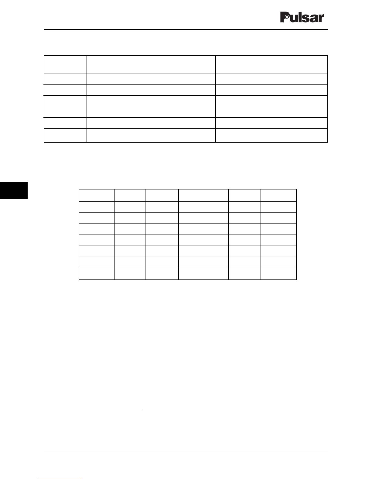
Receiver Logic Module
Place the Receiver Logic Module on an extender
board and set the input signal to 250 kHz, or the
required frequency, at a level of 112 mVrms,
making sure the carrier level meter reads 0 dB.
To test the Phase Comparison Units (Only),
complete the five steps depicted in Table 7-9.
To test the 2-Frequency Directional Comparison
Units (Only), complete the 11 steps depicted in
Table 7-10.
To test the 3-Frequency Directional Comparison
Units (Only), complete the six steps depicted in
Table 7-11. Use an input frequency of 250 kHz
or the center frequency.
Page 7–8 December 2004
TCF–10B System Manual
Te chnologies, Inc.
† On 3-frequency units (OFF).
* Should just light at this level. This is a low signal clamp on a 10 dBm reduction of signal; you may set other levels as
required.
Note: It is recommended that the Receiver Logic pre-trip time delay be for a minimum of 4 ms for
Direct Transfer Trip Applications. Refer to Receiver Logic Section for settings.
SW1-6 SW1-7 SW1-8 BANDWIDTH SHIFT 2F/3F
OFF OFF OFF 380 Hz 100 Hz 2F
OFF OFF ON 800 Hz 250 Hz 2F
OFF ON OFF 1600 Hz 500 Hz 2F
OFF ON ON 800 Hz 250 Hz 3F
ON OFF OFF 1600 Hz 500 Hz 3F
ON OFF ON 800 Hz 100 Hz 2F
ON ON OFF 1600 Hz 250 Hz 2F
Table 7-8. FSK Receiver (SW1-1 set to the OFF position).
Table 7-7. FSK Receiver (SW1-1 settings).
SWITCH
SETTING
OFF ON
SW1-1 FSK AM
SW1-2 NO VOICE ADAPTER VOICE ADAPTER
SW1-3 DTT (50 ms D.O. on noise clamp) UB (10 ms D.O. on noise clamp)
UB 2F or 3 Frequency
SW1-4 DIRECTIONAL COMPARISON RELAYING PHASE COMPARISON RELAYING
SW1-5 SHIFT DOWN TO TRIP 2F or 3F SHIFT UP TO TRIP 2F only
Page 98

December 2004 Page 7–9
Chapter 7. Design Verification Tests
7
* + V (Nominal) outputs equals the voltage applied to the TB1-1, usually station battery.
Rcvr Logic CLI/Discrim. Solid State Outputs Low
LEDs LEDs Signal
Trip – Trip + Noise Low Level Noise Trip – Trip + Contact
1) Check initial LED, output, and contact states:
OFF OFF ON OFF + V* + V* 0V 0V OPEN
2) Remove input signal from chassis; observe states as follows:
ON ON ON ON + V* 0V + V* + V* CLOSED
3) Open SW1-3 on Receiver Logic Module; observe states as follows:
OFF OFF ON ON + V* 0V 0V 0V CLOSED
4) Close SW1-3 (SKBU) and re-connect input signal to chassis. Set input frequency to
250.500 kHz (EWB), or 250.250 kHz (WBWS); or required frequency + 500 Hz (EWB), or
required frequency + 250 Hz (WBWS). Observe states as follows:
ON OFF OFF OFF 0V + V* + V* 0V OPEN
5) Set input frequency to 249.500 kHz (EWB), or 249.750 kHz (WBWS); or required frequency 500 Hz (EWB), or required frequency -250 Hz (WBWS). Observe states as follows:
OFF ON OFF OFF 0V + V* 0V + V
*
OPEN
Table 7-9. Phase Comparison Units (Only) Testing.
Good
Channel
OFF
OFF
OFF
ON
ON
Page 99
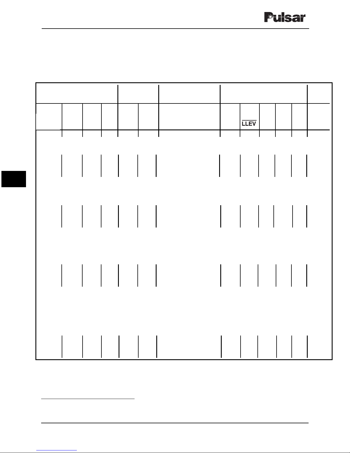
Page 7–10 December 2004
TCF–10B System Manual
Te chnologies, Inc.
Rcvr Logic CLI/Disc Optional
LEDs. LEDs EM Outputs Solid State Outputs
Low
Cbk Cbk Trp Sig
Grd Trp Trp Noise LLev 123456Noise Trp Grd 2 Cont
1) Check initial LED, output, and contact states:
OFF OFF OFF ON ON ( open ) + V* 0V 0V 0V 0V OP
2) Set input frequency to 250.500 kHz (EWB), or 250.250 kHz (WBWS), or 250.100 kHz (NB or
WBNS); or required frequency + 500 Hz (EWB), or required frequency + 250 Hz (WBWS), or
required frequency + 100 Hz (NB or WBNS). Observe states as follows:
ON OFF OFF OFF OFF CL CL CL OP OP OP 0 V + V* 0V + V* 0V OP
3) Set input frequency to 250.000 kHz. Then set input frequency to 249.500 kHz (EWB), or
249.750 kHz (WBWS), or 249.900 kHz (NB or WBNS); or required frequency -500 Hz (EWB), or
required frequency -250 Hz (WBWS) or required frequency -100 Hz (NB or WBNS). Observe
states as follows:
OFF OFF ON OFF OFF ( open ) 0 V + V* + V* 0V 0V OP
4) Set input frequency to 250.500 kHz (EWB), or 250.250 kHz (WBWS), or 250.100 kHz (NB or
WBNS); or required frequency +500 Hz (EWB), or required frequency +250 Hz (WBWS), or
required frequency +100 Hz (NB or WBNS). Then quickly shift input frequency to 249.500 kHz
(EWB), or 249.750 kHz (WBWS), or 249.900 (NB or WBNS); or required frequency -500 Hz
(EWB), or required frequency -250 Hz (WBWS), or required frequency -100 Hz (NB or WBNS).
Observe states as follows:
OFF ON ON OFF OFF OP OP OP CL CL CL 0V + V* + V*0V + V* OP
Table 7-10. 2-Frequency Directional Comparison or Direct Transfer Trip Units (Only) Testing.
* + V (Nominal) outputs equals the voltage applied to the TB1-1, usually station battery.
Good
Channel
OFF
ON
ON
ON
Page 100

December 2004 Page 7–11
Chapter 7. Design Verification Tests
7
Rcvr Logic CLI/Disc Optional
LEDs. LEDs EM Outputs Solid State Outputs
Low
Cbk Cbk Trp Sig
Grd Trp Trp Noise LLev 123456Noise Trp Grd 2 Cont
5) Set input frequency to 250.500 kHz (EWB), or 250.250 kHz (WBWS), or 250.100 kHz (NB or
WBNS); or required frequency + 500 Hz (EWB), or required frequency + 250 Hz (WBWS), or
required frequency + 100 Hz (NB or WBNS). Remove signal from chassis. Observe the TRIP
LED on the Receiver Logic module, and the TRIP 2 SS Output. Neither should blink when
signal is removed. Observe states as follows:
OFF OFF OFF ON ON ( open ) + V* 0V 0V 0V 0V CL
6) Close SW2-4 and open SW2-5 (GBT without override). Reconnect the signal to the chassis.
Observe states as follows:
ON OFF OFF OFF OFF CL CL CL OP OP OP 0V + V* 0V + V* 0V OP
7) Set input frequency as shown in Step 3 (above). Observe states as follows:
OFF OFF ON OFF OFF ( open ) 0V + V* + V* 0V 0V OP
8) Set input frequency as shown in Step 4 (above). Observe states as follows:
OFF ON ON OFF OFF OP OP OP CL CL CL 0V + V* + V* 0V + V* OP
9) Set input frequency as shown in Step 3 (above). Observe states as follows:
OFF ON ON OFF OFF OP OP OP CL CL CL 0V + V* + V* 0V + V* OP
10) Close SW2-1 and SW2-2 (500 ms). Set input frequency to 250.500 kHz (EWB), or 250.250 kHz
(WBWS), or 250.100 kHz (NB or WBNS); or required frequency +500 Hz (EWB), or required
frequency +250 Hz (WBWS), or required frequency +100 Hz (NB or WBNS). Observe states as
follows:
ON OFF OFF OFF OFF CL CL CL OP OP OP 0V + V* 0 V + V*0V OP
11) Remove signal from chassis. Observe the TRIP LED and the TRIP 2 SS Output. Both must
blink when signal is removed.
Table 7-10. 2-Frequency Directional Comparison or Direct Transfer Trip Units (Only) Testing (Cont’d).
* + V (Nominal) outputs equals the voltage applied to the TB1-1, usually station battery.
Good
Channel
OFF
ON
ON
ON
ON
ON
OFF
 Loading...