

Page 1

TC–10B
FREQUENCY-PROGRAMMABLE
ON/OFF CARRIER
TRANSMITTER/RECEIVER
System Manual
CC44–VER06
(Replaces CC44–VER05)
Technologies, Inc.
4050 N.W. 121st Avenue
Coral Springs, FL U.S.A. 33065
1–800–785–7274
www.pulsartech.com
Printed October 2003
Page 2

Technologies, Inc.
Page 3

1
Product Description
2
Applications and Ordering Information
3
Installation
4
Test Equipment
5
Installation/Adjustment Procedures
6
Signal Path
7
Design Verification Tests
8
Maintenance
9
Power Supply Module
10
Keying Module
11
Transmitter Module
12
10W PA Module
13
RF Interface Module
14
Universal Receiver Module
15
Receiver (solid state) Output Module
16
Universal Checkback Module
17
Optional Voice Adapter Module
TC–10B
System Manual
Table
of
Contents
Page 4

Page ii October 2003
Technologies, Inc.
Important Change Notification
This document supersedes the TC–10B Frequency-Programmable On/Off Carrier Transmitter/ Receiver
System Manual CC44–VER05. The following list shows the most recent publication date for each chapter.
Publication dates in bold type indicate changes to that chapter. For these chapters, the specific pages that
have changed are listed for easy reference. Note that only significant changes, i.e., those changes which
affect the technical use and understanding of the document and the TC–10B equipment, are reported.
Changes in format, typographical corrections, minor word changes, etc. are not reported. Note also that in
some cases text and graphics may have flowed to a different page than in the previous publication due to
formatting or other changes. The page numbers below show the current pages on which the reported
changes appear.
Each reported change is identified in the document by a change bar, || placed to its immediate left and/or
right, as shown on this page.
Chapter Number & Title Publication Date Pages with Changes
|| Front Section October 2003 ii, v
1. Product Description October 2000
|| 2. Applications and Ordering Information October 2003 2-6, 17, 20
3. Installation October 2002
4. Test Equipment October 2000
5. Installation/Adjustment procedures October 2002
6. Signal Path October 2002
7. Design Verification Tests October 2002
8. Maintenance September 1996
9. Power Supply Module January 1996
10. Keying Module January 1996
11.Transmitter Module October 2002
12. 10W PA Module October 2002
13. RF Interface Module January 1996
14. Universal Receiver Module October 2002
15. Receiver (solid state) Output Module April 1997
||16. Universal Checkback Module October 2003 16-2, 4, 6, 7, 9, 11, 14, 37,
38, 39, 42, 43
17. Optional Voice Adapter Module October 2000
Page 5

October 2003 Page iii
TC–10B System Manual
W
e recommend that you become acquainted with the information in this manual before energizing your TC–10B system. Failure to do so may result in injury to personnel or damage to
the equipment, and may affect the equipment warranty. If you mount the carrier set in a
cabinet, it must be bolted to the floor or otherwise secured before you swing out the equipment, to
prevent the installation from tipping over.
You should not remove or insert printed circuit modules while the TC–10B is energized. Failure to
observe this precaution can result in undesired tripping output and can cause component damage.
PULSAR does not assume liability arising out of the application or use of any product or circuit
described herein. PULSAR reserves the right to make changes to any products herein to improve reliability, function or design. Specifications and information herein are subject to change without notice.
All possible contingencies which may arise during installation, operation, or maintenance, and all
details and variations of this equipment do not purport to be covered by this manual. If you desire
further information regar ding a particular installation, operation, or maintenance of equipment, please
contact your local Pulsar Technologies, Inc. representative.
Copyright ©
By Pulsar Technologies, Inc. U.S.A.
Published 2002
ALL RIGHTS RESERVED
PULSAR does not convey any license under its patent rights nor the rights of others.
!
IMPORTANT
ESD Warning!
YOU MUST BE PROPERLY GROUNDED, TO PREVENT DAMAGE FROM
STATIC ELECTRICITY, BEFORE HANDLING ANY AND ALL MODULES OR
EQUIPMENT FROM PULSAR.
All semiconductor components used, are sensitive to and can be damaged by the
discharge of static electricity. Be sure to observe all Electrostatic Discharge (ESD)
precautions when handling modules or individual components.
Page 6

PREFACE
Scope
This manual describes the functions and features of the TC–10B Power Line Carrier T ransmitter/Receiver.
It is intended primarily for use by engineers and technicians involved in the installation, alignment,
operation, and maintenance of the TC–10B.
Equipment Identification
The TC–10B equipment is identified by the Catalog Number on the TC–10B chassis nameplate. You can
decode the Catalog Number using the information in Chapter 2.
Production Changes
When engineering and production changes are made to the TC–10B equipment, a revision notation
(Sub number) is reflected on the style number and related schematic diagram. A summary of all Sub
numbers for the particular release is shown on the following page.
Warranty
Our standard warranty extends for 60 months after shipment. For all repaired modules or advance replacements, the standard warranty is 90 days or the remaining warranty time, whichever is longer. Damage
clearly caused by improper application, repair, or handling of the equipment will void the warranty.
Equipment Return & Repair Procedure
To return equipment for repair or replacement:
1. Call your PULSAR representative at 1–800–785–7274.
2. Request an RMA number for proper authorization and credit.
3. Carefully pack the equipment you are returning.
Repair work is done most satisfactorily at the factory. When returning any equipment, pack it in
the original shipping containers if possible. Be sure to use anti-static material when packing the
equipment. Any damage due to improperly packed items will be charged to the customer, even
when under warranty.
Pulsar Technologies, Inc. also makes available interchangeable parts to customers who are
equipped to do repair work. When ordering parts (components, modules, etc.), always give the
complete PULSAR style number(s).
4. Make sure you include your return address and the RMA number on the package.
5. Ship the package(s) to:
Pulsar Technologies, Inc.
Communications Division
4050 N.W. 121st Avenue
Coral Springs, FL U.S.A. 33065
Page iv October 2003
Technologies, Inc.
Page 7

October 2003 Page v
TC–10B System Manual
Overview of this Publication
Chapter 1 – Product Description and specifications
Chapter 2 – Applications and related catalog numbers for ordering
Chapter 3 – Installation
Chapter 4 – Test equipment
Chapter 5 – Installation/adjustment procedures
Chapter 6 – Signal path
Chapter 7 – Design verification tests
Chapter 8 – Maintenance procedures
Chapters 9-17 – Module circuit descriptions and troubleshooting procedures
The TC–10B circuitry is divided into seven (7) standard modules. In addition, Universal Checkback, TTL
Transmitter and Voice Adapter modules are available as options. (See Figure 6-1, for a Functional Block
Diagram.)
Contents of Carrier Set
The TC–10B carrier set includes the style numbers, listed below, with appropriate sub numbers representing revision levels. (To determine related style numbers, you may also refer to Table 2-3.)
Module Style Sub Number
Power Supply 1617C38 GXX 03 ||
Keying 1606C29 G01 11
Transmitter 1610C01 G01 15 ||
TTL Transmitter 1610C01 G02 15 ||
10W PA 1606C33 G01 21
RF Interface 1609C32 G01 09
Universal Receiver C020-RXVMN-203 08 ||
Receiver Output CC20-RXSMN-001 02 ||
Universal Checkback CC20-UCBMN-001 07 ||
Voice Adapter C020-VADMN-001 04 ||
Trademarks
All terms mentioned in this book that are known to be trademarks or service marks are listed below.
In addition, terms suspected of being trademarks or service marks have been appropriately capitalized. Pulsar Technologies, Inc. cannot attest to the accuracy of this information. Use of a term in this
book should not be regarded as affecting the validity of any trademark or service mark.
IBM and PC are registered trademarks of the International Business Machines Corporation.
Page 8

FIGURES
Figure No. Page No.
1-1 TC–10B Chassis and Control Panels with Optional Universal Checkback
and Voice Adapter Modules . . . . . . . . . . . . . . . . . . . . . . . . . . . . . . . . . . . . . . . . .1-9
2-1 Directional-Comparison Blocking, Basic Elements and Logic Diagrams . . . . . . .2-2
2-2 Phase-Comparison Blocking, Basic Elements . . . . . . . . . . . . . . . . . . . . . . . . . . .2-3
2-3 Single Phase Comparison Blocking, Current Only Operation . . . . . . . . . . . . . . .2-4
2-4 Single Phase-Comparison Blocking, Distance-Supervised Operation . . . . . . . . . .2-5
2-5 Simplified Application Schematic (Scheme A) . . . . . . . . . . . . . . . . . . . . . . . . .2-11
2-6 Simplified Application Schematic (Scheme B) . . . . . . . . . . . . . . . . . . . . . . . . .2-12
2-7 Simplified Application Schematic (Scheme C) . . . . . . . . . . . . . . . . . . . . . . . . .2-13
2-8 Simplified Application Schematic (Scheme D) . . . . . . . . . . . . . . . . . . . . . . . . .2-14
2-9 Simplified Application Schematic (Scheme E) . . . . . . . . . . . . . . . . . . . . . . . . . .2-15
2-10 Simplified Application Schematic (Scheme F) . . . . . . . . . . . . . . . . . . . . . . . . . .2-16
2-11 Simplified Application Schematic (Scheme G) . . . . . . . . . . . . . . . . . . . . . . . . .2-17
2-12 Simplified Application Schematic (Scheme H) . . . . . . . . . . . . . . . . . . . . . . . . .2-18
2-13 Simplified Schematic (Scheme K) . . . . . . . . . . . . . . . . . . . . . . . . . . . . . . . . . . .2-19
2-14 Simplified Applications Schematic (Scheme L) . . . . . . . . . . . . . . . . . . . . . . . . .2-20
2-15 Receiver Output Typical Connections for Microprocessor based relays . . . . . . .2-21
2-16 Receiver Outputs w/External Resistors for Electro-mechanical relays . . . . . . . .2-21
3-1 Rear Panel – Mother Board . . . . . . . . . . . . . . . . . . . . . . . . . . . . . . . . . . . . . . . . .3-2
3-2 Cable Termination Diagram . . . . . . . . . . . . . . . . . . . . . . . . . . . . . . . . . . . . . . . .3-4
3-3 Mechanical Outline Drawing . . . . . . . . . . . . . . . . . . . . . . . . . . . . . . . . . . . . . . . .3-9
3-4 Connection Drawing and Jumper Options (Sheet 1 of 2). . . . . . . . . . . . . . . . . .3-10
3-5 Connection Drawing and Jumper Options (Sheet 2 of 2). . . . . . . . . . . . . . . . . . .3-11
4-1 Extender Board . . . . . . . . . . . . . . . . . . . . . . . . . . . . . . . . . . . . . . . . . . . . . . . . . .4-2
6-1 Interconnection and Block Diagram . . . . . . . . . . . . . . . . . . . . . . . . . . . . . . . . . .6-6
9-1 Power Supply Front Panel . . . . . . . . . . . . . . . . . . . . . . . . . . . . . . . . . . . . . . . . . .9-1
9-2 Power Supply Component Location . . . . . . . . . . . . . . . . . . . . . . . . . . . . . . . . . . .9-3
9-3 Power Supply Schematic . . . . . . . . . . . . . . . . . . . . . . . . . . . . . . . . . . . . . . . . . . .9-4
10-1 Keying Module Front Panel . . . . . . . . . . . . . . . . . . . . . . . . . . . . . . . . . . . . . . . .10-1
10-2 Keying PC Board . . . . . . . . . . . . . . . . . . . . . . . . . . . . . . . . . . . . . . . . . . . . . . . .10-5
10-3 Keying Schematic . . . . . . . . . . . . . . . . . . . . . . . . . . . . . . . . . . . . . . . . . . . . . . .10-6
11-1 Transmitter Front Panel . . . . . . . . . . . . . . . . . . . . . . . . . . . . . . . . . . . . . . . . . . .11-1
11-2 Optional TTL Module Front Panel . . . . . . . . . . . . . . . . . . . . . . . . . . . . . . . . . . .11-4
11-3 Transmitter PC Board . . . . . . . . . . . . . . . . . . . . . . . . . . . . . . . . . . . . . . . . . . . .11-6
Page vi October 2003
Technologies, Inc.
Page 9

11-4 Transmitter Schematic . . . . . . . . . . . . . . . . . . . . . . . . . . . . . . . . . . . . . . . . . . . .11-7
11-5 Transmitter Block Diagram . . . . . . . . . . . . . . . . . . . . . . . . . . . . . . . . . . . . . . . .11-8
11-6 TTLTransmitter PC Board . . . . . . . . . . . . . . . . . . . . . . . . . . . . . . . . . . . . . . . . .11-9
11-7 TTLTransmitter Schematic . . . . . . . . . . . . . . . . . . . . . . . . . . . . . . . . . . . . . . .11-10
12-1 10W PA Module Front Panel . . . . . . . . . . . . . . . . . . . . . . . . . . . . . . . . . . . . . . .12-1
12-2 10W PA PC Board . . . . . . . . . . . . . . . . . . . . . . . . . . . . . . . . . . . . . . . . . . . . . . .12-4
12-3 10W PA Schematic . . . . . . . . . . . . . . . . . . . . . . . . . . . . . . . . . . . . . . . . . . . . . .12-5
13-1 RF Interface Front Panel . . . . . . . . . . . . . . . . . . . . . . . . . . . . . . . . . . . . . . . . . .13-1
13-2 RF Interface PC Board . . . . . . . . . . . . . . . . . . . . . . . . . . . . . . . . . . . . . . . . . . .13-3
13-3 RF Interface Schematic . . . . . . . . . . . . . . . . . . . . . . . . . . . . . . . . . . . . . . . . . . .13-4
14-1 Universal Receiver Simplified Signal Flow Diagram . . . . . . . . . . . . . . . . . . . . .14-1
14-2 Universal Receiver Front Panel . . . . . . . . . . . . . . . . . . . . . . . . . . . . . . . . . . . . .14-2
14-3 Universal Receiver Location of SW1 Dip switch & J3 . . . . . . . . . . . . . . . . . . .14-7
15-1 Receiver Output Module — Simplified Signal Flow Diagram . . . . . . . . . . . . . .15-1
15-2 Receiver Output Module Front Panel . . . . . . . . . . . . . . . . . . . . . . . . . . . . . . . . .15-2
15-3 Receiver Output PC Board . . . . . . . . . . . . . . . . . . . . . . . . . . . . . . . . . . . . . . . . .15-6
15-4 Receiver Output Schematic . . . . . . . . . . . . . . . . . . . . . . . . . . . . . . . . . . . . . . . .15-7
16-1 Universal Checkback as part of a TC-10B . . . . . . . . . . . . . . . . . . . . . . . . . . . . .16-4
16-2 Maximum Checkback Configuration with Timed Communications Mode . . . . . .16-5
16-3 Maximum Checkback Configuration with Coded Communications Mode . . . . .16-5
16-4 Universal Checkback Module Front panel Controls and Indicators . . . . . . . . . . .16-5
16-5 Initial Communication with the Checkback Module . . . . . . . . . . . . . . . . . . . . .16-12
16-6 Get Event Screen . . . . . . . . . . . . . . . . . . . . . . . . . . . . . . . . . . . . . . . . . . . . . . .16-15
16-7 Example of a Remote Logon . . . . . . . . . . . . . . . . . . . . . . . . . . . . . . . . . . . . . .16-16
16-8 Universal Checkback Module –Timed Sequence (Master initiated) . . . . . . . . . .16-27
16-9 Universal Checkback Module –Timed Sequence (Remote 1 initiated) . . . . . . . .16-28
16-10 Universal Checkback Module simplified Component Layout . . . . . . . . . . . . . .16-42
16-11 Universal Checkback Module Block Diagram . . . . . . . . . . . . . . . . . . . . . . . . .16-43
17-1 Voice Adapter Module — Simplified Signal Flow Diagram . . . . . . . . . . . . . . . .17-1
17-2 Voice Adapter Module Front Panel . . . . . . . . . . . . . . . . . . . . . . . . . . . . . . . . . . .17-4
17-3 Voice Adapter Module PC Board (C020VADMN) . . . . . . . . . . . . . . . . . . . . . . .17-6
17-4 Voice Adapter Module Schematic (C030VADMN1 Sheet 1 of 2) . . . . . . . . . . . .17-7
17-5 Voice Adapter Module Schematic (C030VADMN2 Sheet 2 of 2) . . . . . . . . . . . .17-8
17-6 Connections for Remote Phone and External Alarm . . . . . . . . . . . . . . . . . . . . . .17-9
17-7 External Alarm Circuit for Use with Module Front Panel Jack . . . . . . . . . . . . .17-10
17-8 Handset Schematic . . . . . . . . . . . . . . . . . . . . . . . . . . . . . . . . . . . . . . . . . . . . . .17-10
October 2003 Page vii
TC–10B System Manual
Page 10

TABLES
Table No. Page No.
1-1 Transmitter/Receiver Specifications. . . . . . . . . . . . . . . . . . . . . . . . . . . . . . . . . . .1-3
1-2 Keying Specifications . . . . . . . . . . . . . . . . . . . . . . . . . . . . . . . . . . . . . . . . . . . . .1-4
1-3 Receiver Output Specifications . . . . . . . . . . . . . . . . . . . . . . . . . . . . . . . . . . . . . . .1-5
1-4 Alarm & Level Option Specifications . . . . . . . . . . . . . . . . . . . . . . . . . . . . . . . . . .1-5
1-5 Checkback Option Specifications . . . . . . . . . . . . . . . . . . . . . . . . . . . . . . . . . . . . .1-5
1-6 Voice Adapter Option Specifications . . . . . . . . . . . . . . . . . . . . . . . . . . . . . . . . . .1-6
1-7 Environmental Specifications . . . . . . . . . . . . . . . . . . . . . . . . . . . . . . . . . . . . . . . .1-6
1-8 Altitude Dielectric Strength De-Rating for Air Insulation . . . . . . . . . . . . . . . . . . .1-7
1-9 Altitude Correction for Maximum Temperature of Cooling Air . . . . . . . . . . . . . .1-7
1-10 Power Requirement Specifications . . . . . . . . . . . . . . . . . . . . . . . . . . . . . . . . . . . .1-8
1-11 Weight and Dimension Specifications . . . . . . . . . . . . . . . . . . . . . . . . . . . . . . . . .1-8
2-1 Directional Comparison Schemes for External and Internal Faults. . . . . . . . . . . . .2-3
2-2 TC–10B Catalog Numbers . . . . . . . . . . . . . . . . . . . . . . . . . . . . . . . . . . . . . . . . . .2-8
2-3 TC–10B Catalog Numbers/Module Style Numbers . . . . . . . . . . . . . . . . . . . . . . .2-9
2-4 Voice Adapter Accessories. . . . . . . . . . . . . . . . . . . . . . . . . . . . . . . . . . . . . . . . . .2-10
2-5 Other TC–10B Accessories . . . . . . . . . . . . . . . . . . . . . . . . . . . . . . . . . . . . . . . . .2-10
2-6 External Resistor Requirements – Provided with Chassis, According to Voltage .2-10
3-1 Attenuator Override Jumper Sensitivity Levels . . . . . . . . . . . . . . . . . . . . . . . . . . .3-7
4-1 Recommended Test Equipment . . . . . . . . . . . . . . . . . . . . . . . . . . . . . . . . . . . . . .4-1
7-1 Voltage Specifications . . . . . . . . . . . . . . . . . . . . . . . . . . . . . . . . . . . . . . . . . . . . .7-1
7-2 Universal Checkback Module DIP Switch Settings . . . . . . . . . . . . . . . . . . . . . . . .7-2
7-3 Voltage Levels . . . . . . . . . . . . . . . . . . . . . . . . . . . . . . . . . . . . . . . . . . . . . . . . . . .7-3
7-4 Keying Logic. . . . . . . . . . . . . . . . . . . . . . . . . . . . . . . . . . . . . . . . . . . . . . . . . . . .7-4
7-5 Level Detector and CLI Test Procedure Specifications. . . . . . . . . . . . . . . . . . . . .7-5
7-6 Receiver Output . . . . . . . . . . . . . . . . . . . . . . . . . . . . . . . . . . . . . . . . . . . . . . . . . .7-6
9-1 1617C38 Styles and Descriptions . . . . . . . . . . . . . . . . . . . . . . . . . . . . . . . . . . . . .9-1
10-1 1606C29 Styles and Descriptions . . . . . . . . . . . . . . . . . . . . . . . . . . . . . . . . . . . .10-1
11-1 1610C01 /Styles and Descriptions . . . . . . . . . . . . . . . . . . . . . . . . . . . . . . . . . . .11-1
Page viii October 2003
Technologies, Inc.
Page 11

TABLES, Cont’d
Table No. Page No.
12-1 1606C33 Styles and Descriptions . . . . . . . . . . . . . . . . . . . . . . . . . . . . . . . . . . . .12-1
13-1 1609C32 Styles and Descriptions . . . . . . . . . . . . . . . . . . . . . . . . . . . . . . . . . . . .13-1
14-1 Universal Receiver Style . . . . . . . . . . . . . . . . . . . . . . . . . . . . . . . . . . . . . . . . . .14-1
14-2 Receiver System Specifications . . . . . . . . . . . . . . . . . . . . . . . . . . . . . . . . . . . . .14-3
14-3 ON–OFF Frequency Spacing Specifications (Minimum) . . . . . . . . . . . . . . . . . .14-4
14-4 AM Receiver (SW1-1 set to the ON position . . . . . . . . . . . . . . . . . . . . . . . . . . .14-4
15-1 CC20-RXSMN-001 Styles and Descriptions . . . . . . . . . . . . . . . . . . . . . . . . . . . .15-1
15-2 Output Table . . . . . . . . . . . . . . . . . . . . . . . . . . . . . . . . . . . . . . . . . . . . . . . . . . .15-3
15-3 Receiver Output . . . . . . . . . . . . . . . . . . . . . . . . . . . . . . . . . . . . . . . . . . . . . . . . .15-5
16-1 Universal Checkback Module Style and Description . . . . . . . . . . . . . . . . . . . . . .16-1
16-2 Universal Checkback Module DIPswitch settings . . . . . . . . . . . . . . . . . . . . . . .16-9
16-3 Factory Preset Configuration Options . . . . . . . . . . . . . . . . . . . . . . . . . . . . . . . .16-10
16-4 Primary/Fallback Communications Options . . . . . . . . . . . . . . . . . . . . . . . . . . .16-24
16-5 Test and General Settings . . . . . . . . . . . . . . . . . . . . . . . . . . . . . . . . . . . . . . . . .16-37
16-6 Output States . . . . . . . . . . . . . . . . . . . . . . . . . . . . . . . . . . . . . . . . . . . . . . . . . .16-37
16-7 Test and Communications Options . . . . . . . . . . . . . . . . . . . . . . . . . . . . . . . . . .16-38
16-8 Programmable Output Definitions . . . . . . . . . . . . . . . . . . . . . . . . . . . . . . . . . .16-38
16-9 Times and Intervals . . . . . . . . . . . . . . . . . . . . . . . . . . . . . . . . . . . . . . . . . . . . .16-38
16-10 Information Commands . . . . . . . . . . . . . . . . . . . . . . . . . . . . . . . . . . . . . . . . . .16-38
16-11 Clearing Commands . . . . . . . . . . . . . . . . . . . . . . . . . . . . . . . . . . . . . . . . . . . . .16-39
16-12 Action commands . . . . . . . . . . . . . . . . . . . . . . . . . . . . . . . . . . . . . . . . . . . . . . .16-39
16-13 Logon commands . . . . . . . . . . . . . . . . . . . . . . . . . . . . . . . . . . . . . . . . . . . . . . .16-39
16-14 Help commands . . . . . . . . . . . . . . . . . . . . . . . . . . . . . . . . . . . . . . . . . . . . . . . .16-39
16-15 Networking Troubleshooting . . . . . . . . . . . . . . . . . . . . . . . . . . . . . . . . . . . . . .16-40
17-1 C020-VADMN Styles and Descriptions . . . . . . . . . . . . . . . . . . . . . . . . . . . . . . .17-1
17-2 Voice Adapter Module Electrical Characteristics . . . . . . . . . . . . . . . . . . . . . . . . .17-3
17-3 DIPSwitch Setting Functions . . . . . . . . . . . . . . . . . . . . . . . . . . . . . . . . . . . . . . 17-5
17-4 Default (Normal) Settings for TC-10B Operation . . . . . . . . . . . . . . . . . . . . . . . .17-5
October 2003 Page ix
TC–10B System Manual
Page 12

Technologies, Inc.
Page 13

1.1 Standard Features
The TC–10B frequency-programmable power-line-carrier set offers the following features as standard:
• Programmable over 30–535kHz (in 0.5kHz steps) with direct frequency readout
• Frequencies are easily field-selectable by rotary switches (transmitter) -or- push button (receiver)
•Wideband (1,600Hz) receiver for use with all blocking systems
• Narrow band (800Hz) receiver for use with directional-comparison blocking systems where there
is a need to improve signal-to-noise ratio (SNR)
• High receiver sensitivity: 22.5mV....(Standard setting)
5mV....(High-sensitivity setting)
• Universal keying/receiver output
• 300-2,000Hz range audio channel for maintenance Voice Channel
• Built-in low/high level carrier test switches
•dc-to-dc isolated power supply
• 48, 125, and 250Vdc versions available
1.2 Standard Nomenclature
The standard nomenclature for PULSAR carrier protection equipment is as follows:
Cabinet – contains fixed-racks, swing-racks, or open racks
Rack – contains one or more chassis (e.g., the TC–10B)
Chassis – contains several printed circuit boards, called modules (e.g., Transmitter or Receiver)
Module – contains a number of functional circuits (e.g., Oscillator or Synthesizer)
Circuit – a complete function on a printed circuit board
1.3 TC–10B Chassis
The TC–10B chassis specifications include standard dimensions of:
Height – 5.25” (133.35 mm), requiring 3 rack units, each measuring 1.75” (44.45 mm)
Width – 19.00” (482.6 mm) Depth – 13.50” (342.9 mm)
Each chassis is notched for mounting in a standard relay rack.
Copyright © 2003 Pulsar Technologies, Inc.
Chapter 1. Product Description
1
Page 14
1.4 TC–10B Modules
The TC–10B circuitry is divided into standard modules with optional Voice Adapter, TTL Transmitter and
Universal Checkback modules available, as shown on the Functional Block Diagram (Fig. 6-1). Circuit
descriptions, complete with schematic diagrams, are shown in Chapters 9 through 17 with Sub Numbers
that indicate appropriate revisions for each module, as follows:
Chapter
Module
Schematic
9. Power Supply 1617C38-2
10. Keying 1606C29-7
11. Transmitter 1355D71-8
12. 10W PA 1606C33-20
13. RF Interface 1609C32-8
14. Universal Receiver not user serviceable
15. Receiver Output (Solid State) CC30-RXSMN
16. (Optional) Universal Checkback not user serviceable
17. (Optional) Voice Adapter C030-VADMN
Page 1–2 October 2003
TC–10B System Manual
NOTE
See Chapter 2, Applications and Ordering Information, for ordering information. See Chapter 3,
Installation, for a summary of jumper controls.
Technologies, Inc.
Page 15
1.5 SPECIFICATIONS
The TC–10B meets or exceeds all applicable ANSI/IEEE standards.
1.5.1 Transmitter/Receiver
Table 1-1 lists the Transmitter/Receiver specifications for the TC–10B.
October 2003 Page 1–3
Chapter 1. Product Description
1
Table 1–1. Transmitter/Receiver Specifications.
Frequency Range 30–535 kHz in 0.5 kHz (500Hz) steps, transmitter selection in
100Hz steps
4-Wire Receiver Input Impedance 5,000
Ω or 1,000Ω
RF Output Impedance 50, 75 or 100Ω (nominal unbalanced)
Output Power • 10 watts (max)
• 100 watts (with optional external amplifier)
Frequency Stability ± 10Hz (typical)
Nominal Receiver Bandwidths • Narrow band: (800Hz at 3db points)
• Wide band (1600Hz at 3db points)
• On-Off Phase Comparison (3,500Hz at 3db points)
Harmonic Distortion 55db below full power
Receive Sensitivity
Narrow Band
or • 22.5 mV (min) to 70V (max) Standard setting
Wide Band
•5 mV (min) to 17V (max) High setting
Page 16
Page 1–4 October 2003
TC–10B System Manual
Channel Speed at 15dB Margin, Solid State Output
Narrow Band (800Hz) 3.8ms (pickup) 6.0ms (dropout) typical
Standard (Wide) Band (1,600Hz) 2.4ms (pickup) 3.8ms (dropout) typical
Phase Comparison Band (3,500Hz) 1.3ms (pickup) 1.5ms (dropout) typical
Minimum Channel Spacing
1.5.2 Keying
Table 1-2 shows the TC–10B keying specifications.
Carrier Start, Carrier Stop All optically isolated for operation at 15V, 48V, 125V, or
Auxiliary (Reduced Power) 250Vdc, strappable for either presence or absence of voltage
Keying for keying, as well as carrier start or stop priority (maximum
burden is 20 mA).
Manual Keying Recessed push button switches for carrier start and auxiliary
keying.
Table 1–1. System Specifications (Cont’d).
Table 1–2. Keying Specifications.
Wideband 4 kHz
Narrow band 2 kHz
With Voice Adapter 4 kHz
(both Narrow band
and Wideband)
An external hybrid or other device offering at least 20db rejection of the adjacent channel
must be used in the application
Technologies, Inc.
Page 17
October 2003 Page 1–5
Chapter 1. Product Description
1
1.5.4 Alarm & Level Option
Table 1-4 shows Alarm & Level Option specifications for the TC–10B.
1.5.3 Receiver Outputs
Table 1-3 shows the TC–10B Receiver Output Specifications.
Two independent relaying Both outputs (fully isolated) provide up to 1 A transistor switch
outputs for microprocessor relaying or 200 mA(into 24Ω), 20mA (into
2,200Ω); will operate from any battery supply (20 to 280Vdc)
One receive alarm output One Form A100VA, 125Vdc (maximum)
One carrier level output (optional)
0–100 µA for external indicator
Table 1–3. Receiver Output Specifications.
Alarm Contacts (dc Power Loss, Form Aor B contacts (field strappable) rated 100VA; 0.5 sec
RF “ON”, and Receive at Margin; of dropout delay
3 separate relays)
Carrier Level Indication Meter –20db to +10dB
Reading
Table 1–4. Alarm & Level Option Specifications.
Table 1–5. Universal Checkback Option Specifications.
• PC interface for controlling settings and operation • Automatic checkback tests done either
• On-line help periodically or at user specified times
• User selectable encoded or timed carrier • Loopback test capability
• Three user programmable outputs • Remote communications
• Optional timed communications fallback • Automatic clock synchronization
• Optional low power tests • Optional carrier recovery
1.5.5 Universal Checkback Options
Table 1-5 shows Universal Checkback Option specifications for the TC–10B.
Page 18
Page 1–6 October 2003
TC–10B System Manual
Ambient temperature range of -20 to +60°C (derated per Table 1-9) (ANS C37.90.)
air-contacting equipment
Relative humidity Up to 95% (non-condensing) at 40°C (for 96 hours cumulative)
(ANS/UL 508)
Altitude • Up to 1,500 m (without derating)
• Up to 6,000 m (using Table 1-8 and Table 1-9)
SWC and FAST Transient All external user interfaces meet SWC and FAST Transients of
ANS C37.90.1 and IEC 255-6
Dielectric Only isolated inputs and outputs, and all alarms: 2,500Vdc from
each terminal to ground, derated per Table 1-8.
(IEC 255-5)
Center conductor of coaxial 3,000Vdc impulse level, using 1.2 x 50ms impulse
cable to ground
Electro-Magnetic Interference IEEE Trial-Use-Standard P734/D5/R4 (ANS C37.90.2).
Compatibility:
Table 1–7. Environmental Specifications.
Modulation Amplitude Modulation with compandor
Transmission Half-Duplex
Frequency Response 300Hz to 2 kHz
Signaling Carrier alarm
Table 1–6. Voice Adapter Option Specifications.
1.5.6 Voice Adapter Option
Table 1-6 shows the TC–10B Voice Adapter Option specifications.
1.5.7 Environmental
Table 1-7 shows the TC–10B environmental specifications.
Technologies, Inc.
Page 19
October 2003 Page 1–7
Chapter 1. Product Description
1
Temperatures (Degrees C)
Altitude (Meters) Short-Time Long-Time Difference
From Usual
Usual 1,500 55 40 —
Unusual 2,000 53 38 2
Unusual 3,000 48 33 7
Unusual 4,000 43 28 12
Table 1–9.
Altitude Correction For Maximum
Temperature Of Cooling Air (ANS C93.5).
Altitude (Meters) Correction Factor
1,500 1.00
1,800 0.97
2,100 0.94
2,400 0.91
2,700 0.87
3,000 0.83
3,600 0.79
4,200 0.74
4,800 0.69
5,400 0.64
6,000 0.59
Table 1–8.
Altitude Dielectric Strength
De-Rating for Air Insulation
Page 20
Page 1–8 October 2003
TC–10B System Manual
1.5.8 Power Requirements and Dimensions
Table 1-10 shows the TC–10B power requirement specifications.
Table 1-11 shows the TC–10B weight and dimension specifications.
Transceiver Supply Current (Amps)
At Nominal Voltage
Nominal Permissible
Battery Voltage Receive/ 1 Watt 10 Watt
Voltage Range Standby Transmit Transmit
48/60Vdc 38–70Vdc .630 .940 1.600
110/125Vdc 88–140Vdc .240 .360 .600
220/250Vdc 176–280Vdc .120 .180 .300
Table 1–10. Power Requirement Specifications.
Equipment Net Weight Height Width Depth Rack
lbs Kg inches mm inches mm inches mm Space
Transceiver 21 9.53 5.25 133.4 19.00 482.6 13.50 342.9 3 RU
Table 1–11. Weight and Dimension Specifications.
Technologies, Inc.
Page 21
1
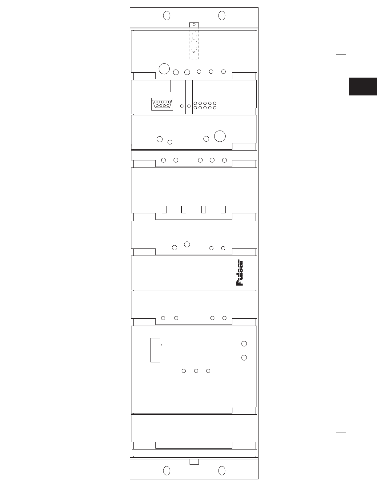
Figure 1–1. TC–10B Chassis and Control Panels with Optional Universal Checkback and Voice Adapter Modules. (1354D16A)
POWER SUPPLY
POWER
INPUT
OUTPUT
+20V
COMMON
–20V
POS. 22
LOOP
HOLD
2 SEC
PC
INTERFACE
CHECKBACK
POS. 20
CALLING
P.B .
T
ALARM
E
S
HL
VOICE ADAPTER
POS. 18
KEY
POS. 17
RECOVER
MAJOR ALRM1MINOR ALRM2RECOVERY3REMOTE LOGON
ALARM
CHECK
RST
TST
T
LL
HL
4
AUDIO
RECEIVE
E
Y
K
LL
CHECK OK
C
PRGM
SET
HANDSET
I
N
G
V
POS. 14
POS. 12
POS. 10
POS. 8
TRANSMITTER
10W POWER AMP
TC–10B
RF INTERFACE
UNIVERSAL RECEIVER
F
POWER
ON-OFF
LINE
kHz
R
E
Q
TRANSMIT
LINE
CARRIER
LINE
COM
+10
U
INPUT
+5
E
N
LEVEL
C
SET
0
Y
X
1
0
0
H
Z
INPUT
COMMON
CC44
RCVR
–15
BLOCK DIAG.
RCVR
COM
–20
1353D16
Technologies, Inc.
AM: MARGIN DETECT
MANUAL
CAT. NO.
S1A1WVAS
–5 dB
–10
SET
LOWER
FRONT VIEW
MADE IN U.S.A.
SIGNAL
FSK: LOW NOISE
CANCEL / RAISE
POS. 3
RCVR OUTPUT
POS. 1
Page 22

Page 1–10 October 2003
TC–10B System Manual
USER NOTES
Technologies, Inc.
Technologies, Inc.
Page 23

2.1 Protective Relay
Applications Using
ON/OFF Carriers
The TC–10B carrier set is particularly suitable for
the following types of protective relay systems:
• Directional-Comparison Blocking
• Phase-Comparison Blocking
• Current Only
• Distance Supervised
2.1.1 Directional-Comparison
Blocking
The basic elements for directional-comparison
blocking systems are shown in Figure 2-1a and
Figure 2-1b. At each terminal, the phase and
ground trip units (P) must be directional and set to
overreach the remote terminal; that is, they must
be set to operate for all internal faults. Nominal
settings of the distance units are 120 to 150
percent of the line. The start units (S) must reach
farther, or be set more sensitively, than the remote
trip units. Thus S
1 must be set more sensitively
than P
2 or reach farther behind bus G. Likewise,
S
2 must be set more sensitively than P1 or reach
farther behind bus H. In any case, the S and P
relays should be similar in type. If the trip unit (P)
is a directional overcurrent ground relay, the start
(S) ground relay should be a similar non-directional overcurrent unit. The same principle applies
for the phase relays.
When the TC–10B ON-OFF power line carrier is
used with these schemes, except for possible
auxiliary functions, no signal is normally trans-
mitted, since the S units operate only during fault
conditions.
Operation of the directional-comparison scheme
(shown in Figure 2-1a and Figure 2-1b) is internal
faults. Subscript 1 indicates relays at station G for
breaker 1; subscript 2, relays at
station H for breaker 2. (Figure 2-1c shows a
solid-state logic version of Figure 2-1b.)
The schemes shown are still widely used for their
flexibility and reliability. Since the communication channel is not required for tripping, internal
faults that might short and interrupt the channel
are not a problem. Over tripping will occur,
however, if the channel fails or is not established
for external faults within the reach of the trip fault
detectors. Since the carrier transmitter is normally
OFF, or non-transmitting, channel failure cannot
be detected until the system is tested or until an
external fault occurs. This limitation can be
overcome by using the optional TC–10B
checkback system with the TC–10B carrier.
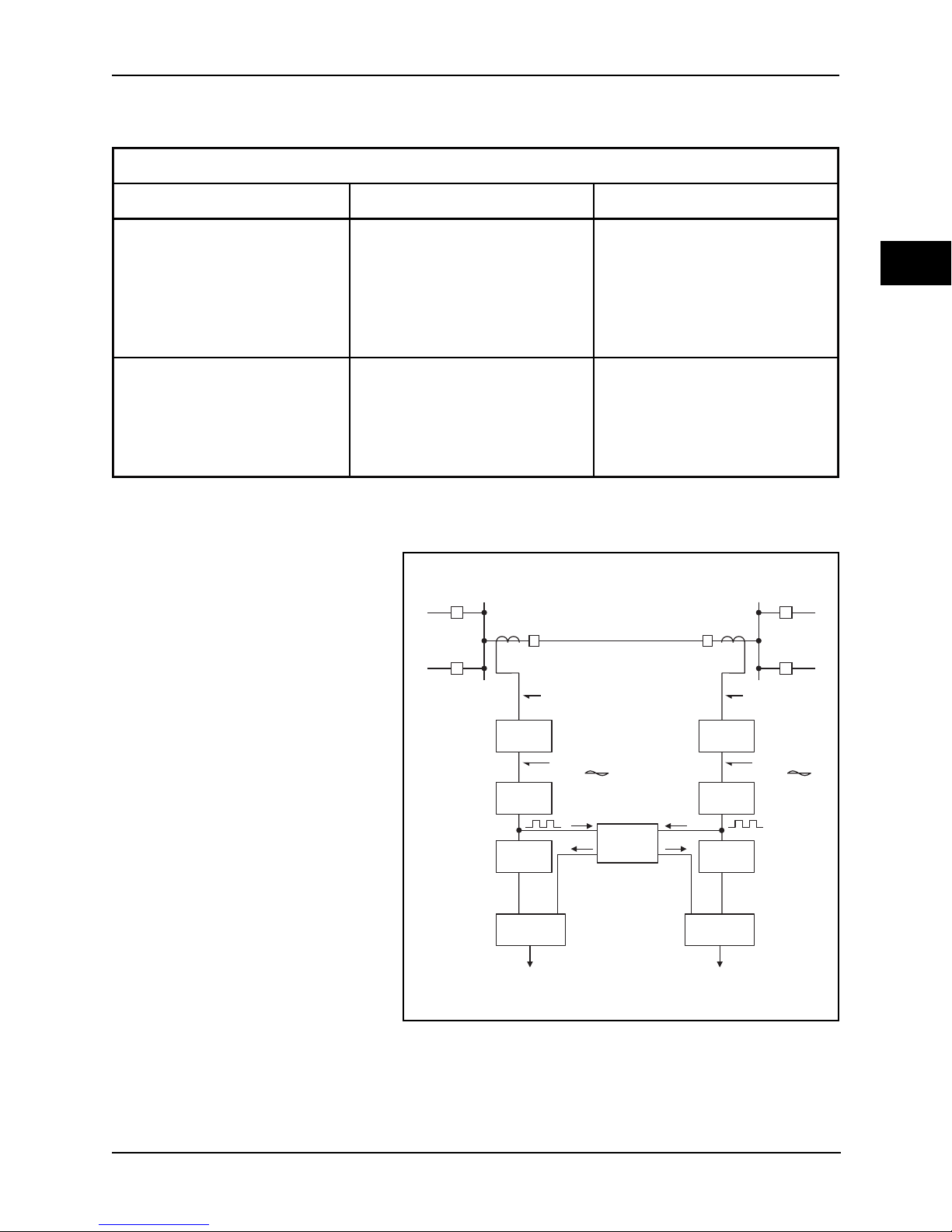
2.1.2 Phase-Comparison Blocking
Basic elements of the phase-comparison systems
are shown in Figure 2-2. The system uses a
composite sequence current network to provide a
single-phase voltage output proportional to the
positive, negative, and zero sequence current
input. Sensitivity to different types of faults
depends on the weighting factors or constants
designed into the sequence current network.
Adjustments to the network are provided.
A squaring amplifier in the controlling relay
converts the single-phase voltage output to a
square wave. The positive voltage portion corresponds to the positive half-cycle of the filter
voltage wave and the zero portion corresponds to
the negative half-cycle. The square wave is used
to key the TC–10B, transmitting to the remote
terminal. The square wave from the remote
terminal is compared to the local square wave,
which has been delayed by an amount equal to the
absolute channel delay time. This comparison of
the local and remote square waves at each
Copyright © 2003 Pulsar Technologies, Inc.
Chapter 2. Applications and Ordering Information
2
Page 24
Page 2–2 October 2003
TC–10B System Manual
Technologies, Inc.
2-1a – Basic Elements for directional-comparison blocking systems.
2-1c – Solid State Logic (per Terminal).
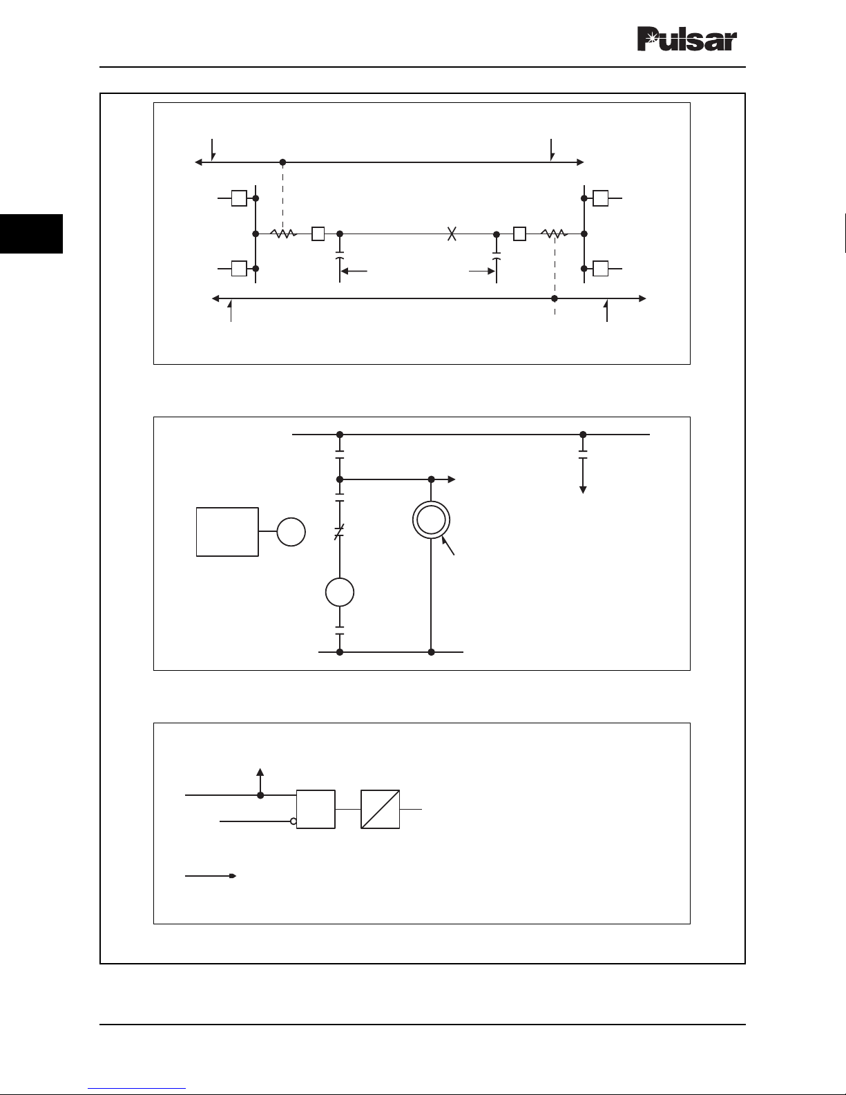
Figure 2–1. Directional-Comparison Blocking, Basic Elements and Logic Diagrams.
2-1b – Contact Logic (per Terminal).
Breaker 1 Channel
Start Fault Detectors (S1)
G
Protected Line
1 2
Breaker 2 Trip Fault Detector (P2)
F
I
Power Line Carrier
Channel
Breaker 1 Trip
Fault Detector (P1)
H
Breaker 2 Channel
Start Fault Detectors (S2)
S
Initiate
Channel
Signal
Channel
Signal
Receiver
RR
P
CS
RR
Trip
Coil
Stop Channel
Signal if
Initiated
Locally
CS
Pick-up
Approximately
13–16 Ms
F
E
52a
Stop Channel Signal if
Initiated Locally
Timer
P
S From
AND
X
Trip
O
Remote Terminal
Via Channel
S Initiate Channel Signal
X – Nominally Between 6–16 Ms
Note: (P) Operation or (S) Signal
Provides an Input 1 on Circuit.
Page 25
terminal determines whether a fault
is internal or external.
Fault detectors are used to determine
whether a fault has occurred and to
supervise tripping. The fault
detectors must be overreaching, i.e.,
set sensitively enough to operate for
all internal phase and ground faults.
Because overcurrent fault detectors
are normally used, voltage transformers are not required. Such a
scheme is current only. Fault
detectors should be set above
maximum load, yet operate for all
internal faults. Distance fault
detectors, which require voltage
transformers, are used on heavyloaded or long lines when distance
supervision is required.
October 2003 Page 2–3
Chapter 2. Applications and Ordering Information
2
Table 2–1. Directional Comparison Schemes for External and Internal Faults.
* For external faults, the CS unit or timer x/o assure that a blocking signal is established.
SCHEME FOR EXTERNAL AND INTERNAL FAULTS
Type of Fault Events at Station G Events at Station H
External (FE)
For external faults, the
CS unit or timer x/o
assure that a blocking
signal is established.
P1operates; S1does not see
fault. Blocking signal received
from station H. RR back
contacts open (or 1 signal
negates AND).
No trip.
S2operates to key transmitter.
Blocking signal sent to station
G. P2does not see fault.
No trip.
Internal (FI) P1operates; S1may or may not
operate, but P1operation
prevents transmission of a
blocking signal.
Breaker 1 tripped.
P2operates, S2may or may not
operate but P2operation
prevents transmission of a
blocking signal.
Breaker 2 tripped.
Figure 2–2. Phase-Comparison Blocking, Basic Elements.
G
1 2
Protected Line
Sequence
Network
Squaring
Amplifier
Three Phase
and Neutral
Single Phase
Output
Delay
Circuit
Channel
Comparison
Circuit
Trip Breaker 1 Trip Breaker 2
Sequence
Network
Squaring
Amplifier
Delay
Circuit
Comparison
Circuit
H
Three Phase
and Neutral
Single Phase
Output
Page 26
Page 2–4 October 2003
TC–10B System Manual
Technologies, Inc.
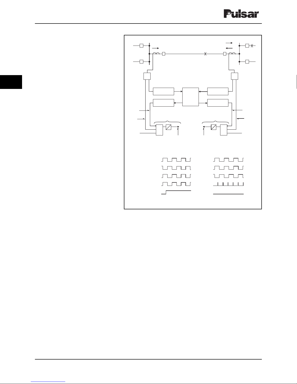
2.1.3 Single PhaseComparison
Blocking, Current
Only
In the current only system, the
TC–10B is used with two overcurrent fault detectors (FD
l and FD
2).
FD
1, the carrier start unit, is set
more sensitively than FD
2 and
permits the local square wave
signal to key the “ON/OFF” carrier
transmitter. FD2, set with a higher
pickup than FD1, is used to arm the
system for tripping. For transmission lines less than 100 miles long,
the FD
2
pickup is set at 125 percent
of FD
1. For lines longer than 100
miles, the FD
2 pickup is set at 200
percent of FD
1. On a three-terminal
line, FD
2 is set at 250% of FD1,
provided the line length between
any two breakers is less than 100
miles. Phase-Comparison cannot
occur until FD
2 operates. The
purpose of the two fault detectors is
to coordinate the comparison of the
local and remote square waves with
the keying of the carrier square
wave. The carrier must be started
before the comparison is allowed
to ensure that the remote square
wave has been received.
The basic operation of the system is
shown in Figure 2-3. FD
1
and FD2at
both terminals operate for an
internal fault (F
I
). The square wave
inputs to the AND from the local
currents are essentially in phase
with those transmitted via the
channel from the remote terminal.
The local square wave turns the
carrier “ON” and “OFF” to provide
the square wave receiver output for
the remote terminal.
A flip flop is energized if the inputs
to the AND continue for 4ms,
providing a continuous trip output
supervised by FD2 operation. The 4ms correspond to a phase
angle difference of 90°, on a 60-Hz base, between the currents at
the two terminals. The currents at the two ends of the line may
be out of phase by up to 90° and still trip. This is a blocking
system, since the receipt of a signal from the channel prevents
tripping. The carrier signal, therefore, does not have to be transmitted through the internal fault. No received signal puts a “1”
on the AND input. With the remote terminals open, this system
provides sensitive instantaneous overcurrent protection for the
entire line. As is characteristic of blocking systems, the channel
is not required for tripping on internal faults.
For an external fault, such as F
E in Figure 2-3, blocking is essen-
tially continuous, since the remote wave input to the AND is
out-of-phase with the local square wave. The secondary ct
currents are essentially out-of-phase for an external fault. The
currents can, however, be in-phase by up to 90
° on a 60-Hz base
and still block.
Figure 2–3.
Single Phase Comparison Blocking, Current Only Operation.
G
FI& F
E
1 2
Fault Detecting Logic
(Figure 2–2)
Transmitter
Receiver
Receiver
Output
Local
Input
Arming Arming
Internal Fault (FI)
(at Terminal G*)
Local Input
to AND
Receiver
Output
Receiver Input
to AND
AND Output
Trip Output
* Equivalent operation and same trip output at Station H.
Comparison Circuit
Basic Logic
4
0
AND AND
Trip Breaker 1 Trip Breaker 2
0
0
0
0
Protected Line
Channel
1
0
1
1
1
F
I
Fault Detecting Logic
(Figure 2–2)
Transmitter
Receiver
Comparison Circuit
Basic Logic
4
0
External Fault (FE)
(at Terminal G*)
0
0
1
0
0
H
F
E
F
I
F
Receiver
Output
Local
Input
1
11
0
0
0
E
Page 27
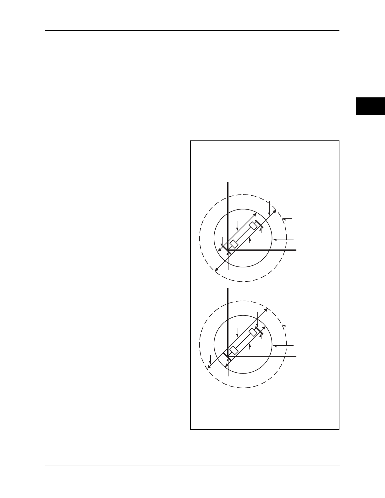
2.1.4 Single-Phase, Distance-
Supervised Comparison
Blocking
A distance-supervised scheme should be used
if the minimum internal three-phase fault
current is less than twice the maximum load
current. Twice maximum load current allows
FD
l to operate positively on the minimum
internal three-phase fault, yet reset when an
external fault is followed by a maximum load
current flowing through the line. The TC–10B
operates in the same manner as when used
with the current-only scheme, except for the
fault detection and arming techniques.
Two sequence current networks and two
distance relays supplement the two overcurrent fault detectors.
One sequence current network responds only
to negative and zero sequence currents,
detecting all phase-to-phase and ground faults
(but not three-phase faults). The output of this
adjustable network operates the conventional
overcurrent FD
l and FD2
fault detectors. The
two distance relays operate only for threephase faults. Thus, FD
2 provides the arming
function for all unbalanced phase and ground
faults, through the adjustable filter, and one of
the distance relays (21P) provides arming for
all three-phase faults.
The second and non-adjustable sequence
current network operates through the squaring
amplifier, providing the local square wave and
the carrier-keyed square wave required for
phase comparison. This signal is keyed by FD
1
and the second distance relay (21S) to provide
the carrier start functions. This second
network responds to positive, negative, and
zero sequence currents. Separate networks
provide greater sensitivity: with phase-tophase faults, for example, more than twice the
sensitivity is gained.
October 2003 Page 2–5
Chapter 2. Applications and Ordering Information
2
Figure 2–4. Single Phase-Comparison Blocking,
Distance-Supervised Operation.
The setting coordination of FDl and FD2 overcurrent
units is the same as for the current-only system.
Settings for the two three-phase distance units are
shown in Figure 2-4. Both 21S and 21Pdistance relays
must be set to overreach both the local and remote
terminal buses; 21S must be set further than 21P, as
shown.
X
Z
C
Z
Z
C
Bus G
A
2
Bus H
1
Z
A
X
21 S at Breaker
21 P at Breaker
R
Z
C
Bus H
Z
A
2
Z
C
1
Z
A
21 S at Breaker
21 P at Breaker
R
Bus G
Page 28

|| 2.1.5 Phase Comparison Relaying
and 20V Auxilliary Power
Supply
|| When ordering a TC-10B for use with phase
comparison relaying, a 20V auxilliary power
supply is provided.
The majority of interfaces between the relay and
the communications equipment are done at the
station battery. If the control battery is 125Vdc,
then the carrier output will be powered up with
125Vdc to provide station battery voltage to the
relay. However, in phase comparison relay
systems, the ratio, of the on and off state, of the
carrier circuit ouptut and the on and off state of the
relay’s keying circuit is critical to provide a square
wave that closely represents the power system ac
wave. Therefore, based on the type of inputs used
on the relay system at the point it interfaces with
the carrier system, this will determine what
voltage level is acceptable. This criticality is on
the order of 500 or less microseconds.
Due to the capacitors typically applied to output
circuits to dampen surges, the higher the voltage
applied, the longer it will take to dissipate the
energy . Therefore, to dissipate this ener gy quickly,
to adhere to the timing requirements for a secure
phase comparison relay system, the use of the
auxilliary 20V power supply is necessary.
Different relay manufacturers’ input circuits may
vary and can conceivably decay fast enough not to
hinder the security of the relay system operation.
However, the energy dissipated will also generate
a significant amount of heat. By utilizing the
auxilliary supply, mounted on the rear of the
carrier unit, it will allow that heat to be outside of
either unit.
Pulsar strongly recommends the application of the
auxilliary power supply for two reasons; decay
time of the energy, and the heating caused by the
dissipation of energy.||
2.2 Special Application
Considerations
Because the TC–10B is “ON/OFF” modulated,
only one frequency (f
C
) is required for line protec-
tion. When applied to three terminal lines, phase
cancellation will occur when two or more transmitters are keyed simultaneously. To prevent this,
you should offset transmitters by ±100Hz, using
the thumbwheel frequency programming
switches. The three frequencies should be:
•f
C
•fC- 100Hz
•f
C
+ 100Hz
When using the TC–10B with the SKBU-1 PhaseComparison, you must offset the transmitter
frequencies from the center frequency by 100 Hz
for all applications. In a two-terminal application,
set the transmitter at one end 100Hz above the
center frequency, and the transmitter at the other
end 100Hz below the center frequency. Thus, the
two transmitters are spaced 200Hz from each
other. For a three terminal line, you should offset
the transmitter as described in the above
paragraph.
The TC–10B does not have an adjustable filter or
hybrid attached to the output of the transmitter.
If you are using the TC–10B in an application
where no other power line carrier equipment is
attached to the power line, then no further action
is required. However, in the application of
Single Comparator Phase Comparison
relaying, the TC–10B is to be operated in the
four-wire mode (see RF Interface Module),
with an external skewed hybrid between transmitter and receiver.
If you are applying the carrier set with other transmitters, coupled through the same tuning
equipment, you must apply a hybrid or a series LC
unit to the transmitter output to isolate the other
transmitters from the TC–10B transmitter. This
will avoid the problems of intermodulation distortion. We suggest that you use a hybrid if the
frequency spacing between all transmitters is
within the bandwidth of the hybrid (usually 6%).
Check the manufacturers instructions for the
actual spacing limitations of the hybrid you are
using. If you cannot use a hybrid, then you may
use a series LC unit to isolate the transmitters. In
this case, the transmitters must have spacing such
that the LC you are using will attenuate the
Page 2–6 October 2003
TC–10B System Manual
Technologies, Inc.
Page 29

external frequencies by at least 20dB (if the other
frequency is a 10 watt transmitter), and 30dB (if
the other frequency is a 100 watt transmitter).
2.3 Ordering Information
The TC–10B carrier is functionally compatible
with earlier type carrier equipment (e.g., KR, TC,
TC-10, TC-10A). That is, you may use the
TC–10B with these other carrier types at the
opposite end of the line, with or without voice
function. You may use the same telephone handset
unit with any of these ON-OFF carrier sets.
You may use the TC–10B carrier set with the
following types of relay systems:
• All Directional-Comparison Blocking
Systems
• Phase-Comparison Blocking Systems,
e.g., SKBU-1 (Requires 45-Vdc power
supply — please see Table 2-5.)
Simplified schematics of typical electro-mechanical systems are shown in Figure 2-5 through
Figure 2-13 (schemes A thru K). These schemes
indicate the different jumper positions required for
particular applications. Simplified connections
between the TC–10B and a microprocessor based
relay are shown in Figure 2-14 (Scheme L).
Figure 2-15 shows the output circuit for microprocessor based relays (1 amp maximum output).
Figure 2-16 shows the resultant output circuit for
48, 125, and 250Vdc systems.
Two variations of TC–10B are available:
(1) Plug-in Voice Adapter Module with signaling
as a push-to-talk maintenance voice channel (see Chapter 17). Atelephone jack is provided
on the Voice Adapter Module, but you may
also use a remote jack or hookswitch. (See
Figure 18-4, Scheme J, for the connection
diagrams.)
(2) Plug-in Universal Checkback Module for
periodic testing of the carrier channel at
programmable intervals (see Chapter 17).
(See Figure 3–3 for connection diagrams.)
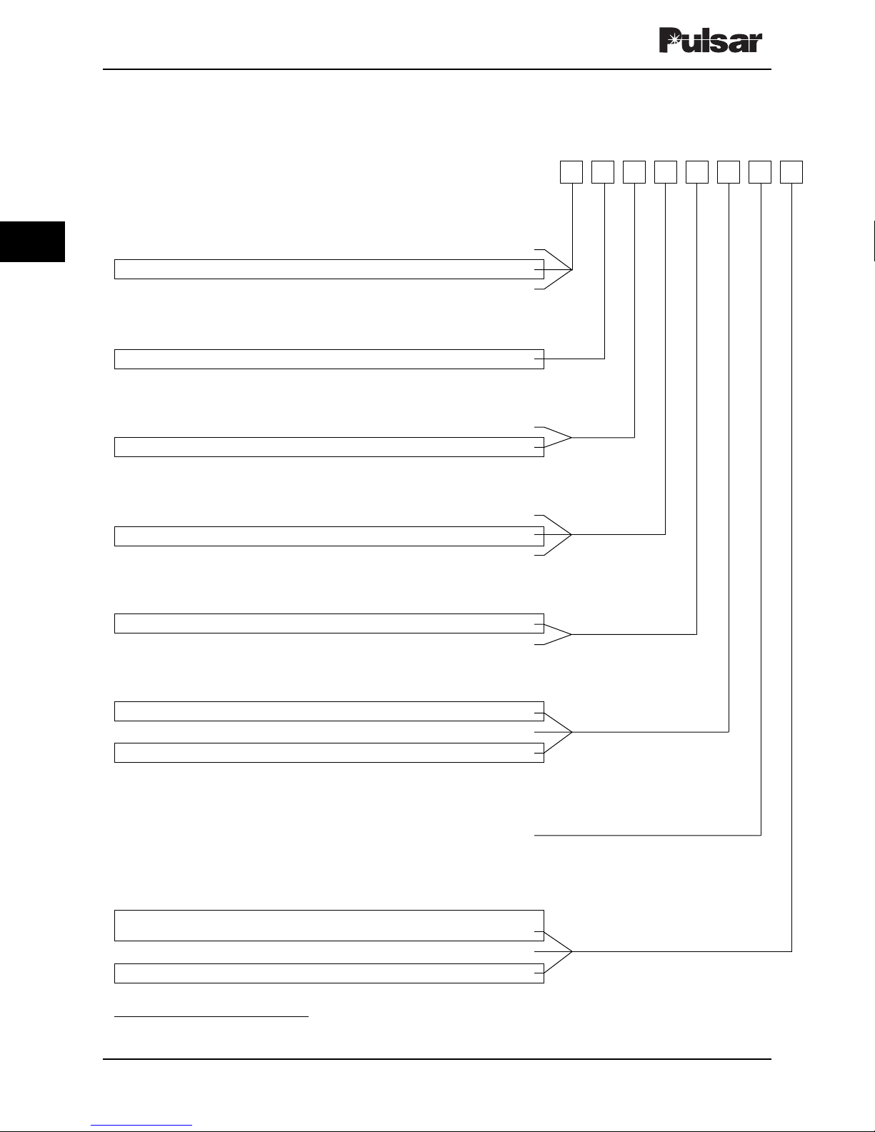
The equipment identification number (catalog
number) is located in the middle of the front panel
(just to the left of the 10W PA Module). The
TC–10B catalog number comprises eight (8) characters, each in a specific position. This number
identifies the unit's technical characteristics and
capabilities, as well as any optional modules
installed in the unit.
Table 2-2 provides a complete listing of the
options for ordering a TC–10B, as well as a
sample catalog number. To order one or more
TC–10Bs, simply identify the features and
optional modules you want for each chassis. For
example, the typical catalog number shown in
Table 2-2 — S1A1WVAS— orders a
TC–10B with the following features:
Basic TC–10B Transmitter/Receiver
Power Output: 10 watt
Universal Checkback: Universal Checkback
Module, PC programmable
dc/dc Converter Power Supply: 110/125Vdc
battery input
Bandwidth (Filter Range): Wideband filter
Voice Adapter: Voice Adapter Module with
signaling
Alarm and Carrier Level Indication: with loss-
of-dc-power alarm relay, R.F. output alarm
relay, received-carrier-level-margin alarm
relay, detect alarm, instrument indicating
carrier level (-20dB to +10dB), carrier level
analog output (0–100 µA) for external instrument
Outputs: Dual transistor-switched outputs (for
use with electro-mechanical carrier auxiliary
relays and microprocessor relays)
Table 2-3 provides a further breakdown of the
TC–10B catalog number by style numbers.
The accessories available for the TC–10B are
listed, along with their style numbers, in Table 2-4
and Table 2-5. To order an accessory, simply give
its style number.
October 2003 Page 2–7
Chapter 2. Applications and Ordering Information
2
Page 30
Page 2–8 October 2003
TC–10B System Manual
Technologies, Inc.
Table 2–2. TC–10B Catalog Numbers
Typical Catalog Number
S 1 A 1 W V A S
Catalog Number Position 12345678
Basic TC–10B Transmitter/Receiver
Solid state programmable transmitter/receiver assembly for
phase- or directional-comparison relaying, or supervisory control S
Self-Adjusting Receiver only V
Transmitter only X
Power Output
10 watt output * 1
Automatic Checkback
Universal Checkback, Personal Computer programmable A
No Checkback Module N
DC/DC Converter Power Supply
48/60Vdc battery input 4
110/125Vdc battery input 1
220/250Vdc battery input 2
Bandwidth (Filter Range)
Wideband filter W
Narrow band filter X
Voice Adapter
Voice Adapter Module with signaling V
No Voice Adapter Module N
Transmission Limitation Circuit T
Alarm and Carrier Level Indication
With loss-of-dc-power alarm relay, R.F.-output alarm relay,
received-carrier-level-margin alarm relay, carrier level A
analog output (0–100 µA) for external instrument
Outputs
Dual transistor-switched outputs (for use with electro-mechanical
carrier auxiliary relays and microprocessor relays) S
Transmitter only chassis N
Phase Comparison Output (20Vdc power supply included) P
Accessories TC–10B/TCF–10B Extender Board . . . . . . . . .Style # 1353D70G01
TC–10B to KR mounting kit . . . . . . . . . . . . . . .Style # 1355D61G01
*For 50 or 100 watt output, see document
CA44-VER03 (Linear Power Amplifier)
Page 31

2
Table 2–3. TC–10B Catalog Numbers/Module Style Numbers.
SorN
S,NorP
A
A
S
1
1
W
V
A
S
V,NorT
WorX
4,1or2
AorN
10 Watts
Automatic Checkback
DC/DC Converter Power Supply
Bandwidth
Voice, Transmit Limiter
Alarm and Carrier Level Indication
Outputs
1
S,VorX
P
Basic Transmitter/Receiver
Position Description Style Number S V X A N 1 2 4 W X V N T S A N 1 2 4 W X V N T
1Receiver Output CC20-RXSMN-001 X X X
3Receiver C020-RXVMN-201 or 203 X X X
8RFInterface 1606C32G01 X X X X
12 10W Power Amp 1606C33G01 X X X
14 Transmitter 1610C01G01 X X X X
Transmitter w/TTL 1610C01G03 X X
17 Keying 1606C29G01 X X X
18 Voice Adapter C020-VADMN-001 X X
Blank Panel 1606C47H03 X X X X
20 Universal Checkback CC20-UCBMN-001 X X
Blank Panel 1606C47H03 X X
22 Power Supply 48Vdc 1617C38G01 X X
Power Supply 125Vdc 1617C38G02 X X
Power Supply 250Vdc 1617C38G03 X X
none 20V Aux. PS-48 to 20Vdc 1610C07G01 X
20V Aux. PS-125 to 20Vdc 1610C07G02 X
20V Aux. PS-250 to 20Vdc 1610C07G03 X
none Chassis Assy. 1353D63G01 X X
10 Nameplate 1496B80H03 X X
none Cover Assy. 1606C49G01 X X
none Resistor Assy. (250Vdc) 1355D01G02 X X
none Resistors (125Vdc) 01R3-3310-43M qty 2 X X
none P.S. Filter C020-BKPA1-001 X X
Page 32

Page 2–10 October 2003
TC–10B System Manual
Technologies, Inc.
Accessories for Voice Adapter Style Number
Sonalert (2,900Hz, 60–250Vdc) SC250J
Telephone Hookswitch 205C266G05
Assembly (panel mounting) with
Noise Canceling Handset
Telephone Handset, Push to Talk, 1353D88G01
Noise Canceling (single prong plug)
Telephone Jack, remote panel 715B674G03
mounting (single prong plug)
Other Accessories Style Number
45V power supply for use with
SKBU-1 Relaying System
48V to 45V 5303D49G05
125V to 45V 5303D49G06
250V to 45V 5303D49G07
Table 2–4. TC–10B Voice Adapter Accessories.
Table 2–5. Other TC–10B Accessories
Carrier Aux. Battery Resistor
Relay Voltage
20 mA (220Ω)48Not Required
20 mA (220Ω) 125 3500Ω, 5W
20 mA (220Ω) 250 9200Ω, 10W & 500Ω, 40W
200 mA (25Ω)48Not Required
200 mA (25Ω) 125 Not Required
200 mA (25Ω) 250 500Ω, 40W
Table 2–6. External Resistor Requirements — Provided with
Chassis, According to Battery Voltage.
Page 33

October 2003 Page 2–11
Chapter 2. Applications and Ordering Information
2
Figure 2–5. TC–10B Simplified Application Schematic – Scheme A (7833C63).
POS
JUMPER
TB6–1
TB6–2
TB7–5
TC–10B
TB6–4
TB6–5
TB7–1 (DC+)
AUTOMATIC CHECKBACK
(SEE FIGURE 6-1 FOR
CONNECTIONS)
TB6–6
TB6–7
TB6–8
TB6–9
TB1–1 (OUTPUT+)
TB4–3 (STOP+)
TB4–5 (LL+)
TB5–7
TB5–8
TB4–1 (START+)
DETECTOR
TB5–9
TB2–3
MARGIN
OUTPUT
TB2–4
TB2–5
TB7–6
TB1–3 (OUTPUT–)
RF OUTPUT
OUTPUT
TB2–6
TB3–1
TB1–8 (OUTPUT–)
ALARM
VOICE ADAPTER
TB3–2
TB5–1
TB4–6 (LL–)
JUMPERS
REMOTE PHONE CONNECTIONS
(SEE FIGURE 17-6)
TB5–2
TB5–3
TB5–4
TB5–5
TB7
–4
TB7
–3
TB2
–2
TB2
–1
TB4–4 (STOP–)
TB4–2 (START–)
TB7–2
(DC–)
BATTERY
VOLTAGE
MODULE
DC FAILURE
KEYING 48 JU1 15
KEYING 125 JU1 48
KEYING 250 JU1 125
ALARM
CLI
EXTERNAL
KEYING 48 JU2 48
KEYING 125 JU2 125
KEYING 250 JU2 250
KEYING 48 JU3 48
KEYING 125 JU3 125
KEYING 250 JU3 250
KEYING —JU4NORM
KEYING — JU5 NORM
KEYING —JU6 NORM
KEYING —JU7STOP
KEYING —JU8 IN
OUTPUT 48 JU1/JU2 48
OUTPUT 125 JU1/JU2 125/250
OUTPUT 250 JU1/JU2 125/250
SCHEME A
SIMPLIFIED K–DAR
UTILIZING COMMON
CARRIER SCHEMATIC
START/STOP CONTROL
1
BATTERY
POSITIVE
CARRIER
LOW
LEVEL
TEST
RC
R
Z1
TEST
CARRIER
Z2
CX
Z3
NOTE
Z5
Z4
CX
CX
PHASE AND
GROUND
+
MA
CARRIER
START
SQ
CSP
CSG
AL
PHASE AND
GROUND
CARRIER
0–30 mA
STOP
RRH
0–300 mA
BATTERY
NEGATIVE
OPTIONAL
IN KA–4
NOTE 1 – EXTERNAL RESISTORS ARE REQUIRED
FOR SOME SYSTEMS, AS SHOWN IN TABLE 2-6. THE
RESISTORS ARE SUPPLIED WITH ALL 125 AND 250
Vdc TC–10B CARRIERS.
NOTE 2 – SOME SCHEMES MAY NOT HAVE CARRIER
CONTINUATION (CX).
Page 34

Page 2–12 October 2003
TC–10B System Manual
Technologies, Inc.
Figure 2–6. TC–10B Simplified Application Schematic – Scheme B (7833C63).
POS
JUMPER
JUMPERS
BATTERY
VOLTAGE
MODULE
KEYING 48 JU1 48
KEYING 125 JU1 125
KEYING 250 JU1 250
KEYING 48 JU2 15
KEYING 125 JU2 48
KEYING 250 JU2 125
KEYING 48 JU3 48
KEYING 125 JU3 125
KEYING 250 JU3 250
KEYING — JU4 NORM
KEYING — JU5 NORM
KEYING — JU6 NORM
KEYING — JU7 STOP
KEYING — JU8 OUT
OUTPUT 48 JU1/JU2 48
OUTPUT 125 JU1/JU2 125/250
OUTPUT 250 JU1/JU2 125/250
TB6–1
TB6–2
TB7–5
TC–10B
AUTOMATIC CHECKBACK
TB6–4
TB6–5
TB7–1 (DC+)
CARRIER
LOW
LEVEL
(SEE FIGURE 6-1 FOR
CONNECTIONS)
TB6–6
TB6–7
TB6–8
TB1–1 (OUTPUT+)
TB4–5 (LL+)
TEST
TB6–9
TB5–7
TB7–6
TB5–8
TB4–3 (STOP+)
DETECTOR
TB5–9
TB2–3
TB4–1 (START+)
MARGIN
OUTPUT
OUTPUT
TB2–4
TB2–5
TB2–6
TB1–3 (OUTPUT–)
TB1–8 (OUTPUT–)
1
NOTE
RF OUTPUT
ALARM
TB3–1
TB3–2
TB4–6 (LL–)
+
AL
VOICE ADAPTER
REMOTE PHONE CONNECTIONS
TB5–1
TB5–2
TB5–3
TB4–4 (STOP–)
RRH
(SEE FIGURE 17-6)
TB5–4
TB4–2 (START–)
TB5–5
TB7
TB7
TB2
TB2
TB7–2
1000
–4
–3
–2
–1
(DC–)
DC FAILURE
BATTERY
RRT
ALARM
CLI
EXTERNAL
NEGATIVE
SIMPLIFIED
SCHEME B
HZ/HZM SCHEMATIC
4000
IOS
23
23
23
BATTERY
POSITIVE
4MFD
250
CBU
CSP CSO
CSO
CSA
CSA
CSA
CSG
CBU UNIT USED ONLY WHEN REMOTE TERMINAL
USES CONTACT OPENING CARRIER START
OPTIONAL
SCHEME SUCH AS KDAR.
NOTE 1 – EXTERNAL RESISTORS ARE REQUIRED
FOR SOME SYSTEMS, AS SHOWN IN TABLE 2-6. THE
RESISTORS ARE SUPPLIED WITH ALL 125 AND 250
Vdc TC–10B CARRIERS.
Page 35

October 2003 Page 2–13
Chapter 2. Applications and Ordering Information
2
Figure 2–7. TC–10B Simplified Application Schematic – Scheme C (7833C63).
TB6–1
TB6–2
TB7–5
TC–10B
TB6–4
TB6–5
AUTOMATIC CHECKBACK
(SEE FIGURE 6-1 FOR
CONNECTIONS)
TB6–6
TB6–7
TB6–8
TB6–9
TB5–7
TB5–8
DETECTOR
TB5–9
TB2–3
MARGIN
OUTPUT
TB2–4
TB2–5
RF OUTPUT
OUTPUT
TB2–6
TB3–1
VOICE ADAPTER
ALARM
TB3–2
TB5–1
JUMPERS
REMOTE PHONE CONNECTIONS
(SEE FIGURE 17-6)
TB5–2
TB5–3
TB5–4
TB5–5
TB7
–4
TB7
–3
TB2
–2
TB2
–1
POS
JUMPER
BATTERY
VOLTAGE
MODULE
DC FAILURE
KEYING 48 JU1 48
KEYING 125 JU1 125
KEYING 250 JU1 250
ALARM
CLI
EXTERNAL
125/250
125/250
JU1/JU2
JU1/JU2
250
125
OUTPUT
KEYING 48 JU2 48
KEYING 125 JU2 125
KEYING 250 JU2 250
KEYING 48 JU3 48
KEYING 125 JU3 125
KEYING 250 JU3 250
KEYING — JU4 INV
KEYING — JU5 NORM
KEYING — JU6 INV
KEYING — JU7 STOP
SIMPLIFIED
SCHEME C
KEYING — JU8 OUT
OUTPUT 48 JU1/JU2 48
OUTPUT
BATTERY
POSITIVE
TB7–1 (DC+)
CARRIER
LOW
LEVEL
TEST
CARRIER
HIGH
LEVEL
TEST
TB1–1 (OUTPUT+)
TB4–5 (LL+)
CARRIER
CARRIER
START
STOP
TB7–6
TB4–1 (START+)
TB4–3 (STOP+)
TB1–3 (OUTPUT–)
TB1–8 (OUTPUT–)
1
NOTE
TB4–6 (LL–)
TB4–4 (STOP–)
+
TB4–2 (START–)
R
CARRIER
TB7–2
(DC–)
AUX.
RELAY
RA
MA
0–30 mA
BATTERY
0–300 mA
NEGATIVE
OPTIONAL
NOTE 1 – EXTERNAL RESISTORS ARE REQUIRED FOR
SOME SYSTEMS, AS SHOWN IN TABLE 2-6. THE RESISTORS
GCY–GCX RELAYING
POSITIVE D.C. KEYING
ARE SUPPLIED WITH ALL 125 AND 250 Vdc TC–10B
CARRIERS.
Page 36

Page 2–14 October 2003
TC–10B System Manual
Technologies, Inc.
Figure 2–8. TC–10B Simplified Application Schematic – Scheme D (7833C63).
TB6–1
TB6–2
TB7–5
TC–10B
TB6–4
TB6–5
AUTOMATIC CHECKBACK
(SEE FIGURE 6-1 FOR
CONNECTIONS)
TB6–6
TB6–7
TB6–8
TB6–9
TB5–7
TB5–8
DETECTOR
TB5–9
TB2–3
MARGIN
OUTPUT
TB2–4
TB2–5
RF OUTPUT
OUTPUT
TB2–6
TB3–1
ALARM
TB3–2
TB5–1
REMOTE PHONE CONNECTIONS
VOICE ADAPTER
(SEE FIGURE 17-6)
TB5–2
TB5–3
JUMPERS
BATTERY
TB5–4
TB5–5
TB7
–4
TB7
–3
TB2
–2
TB2
–1
POS
JUMPER
VOLTAGE
KEYING 48 JU1 48
MODULE
ALARM
DC FAILURE
KEYING 125 JU1 125
KEYING 250 JU1 250
KEYING 48 JU2 48
KEYING 125 JU2 125
CLI
EXTERNAL
KEYING 250 JU2 250
KEYING 48 JU3 48
KEYING 125 JU3 125
KEYING 250 JU3 250
SIMPLIFIED
KEYING — JU4 INV
KEYING —JU5 NORM
KEYING — JU6 INV
SCHEME D
KEYING —JU7STOP
KEYING — JU8 OUT
125/250
JU1/JU2
125
OUTPUT
OUTPUT 48 JU1/JU2 48
125/250
JU1/JU2
250
OUTPUT
TB7–1 (DC+)
TB1–1 (OUTPUT+)
TB4–5 (LL+)
TB4–3 (STOP+)
TB4–1 (START+)
TB7–6
TB4–4 (STOP–)
TB4–2 (START–)
TB4–6 (LL–)
BATTERY
POSITIVE
TB1–3 (OUTPUT–)
NOTE
CARRIER
LOW
LEVEL
TEST
CARRIER
HIGH
1
LEVEL
TEST
TB1–8 (OUTPUT–)
TB7–2
R
R
CARRIER
CARRIER
CARRIER
(DC–)
AUX.
RELAY
START
STOP
RA
GCY–GCX RELAYING
NEGATIVE D.C. KEYING
+
MA
0–30 mA
0–300 mA
OPTIONAL
NOTE 1 – EXTERNAL RESISTORS ARE REQUIRED FOR
SOME SYSTEMS, AS SHOWN IN TABLE 2-6. THE RESISTORS
ARE SUPPLIED WITH ALL 125 AND 250 Vdc TC–10B
BATTERY
NEGATIVE
CARRIERS.
Page 37

October 2003 Page 2–15
Chapter 2. Applications and Ordering Information
2
Figure 2–9. TC–10B Simplified Application Schematic – Scheme E (7833C63).
TB6–1
TB6–2
TB7–5
TC–10B
TB6–4
TB6–5
AUTOMATIC CHECKBACK
(SEE FIGURE 6-1 FOR
CONNECTIONS)
TB6–6
TB6–7
TB6–8
TB6–9
TB5–7
TB5–8
DETECTOR
TB5–9
TB2–3
MARGIN
OUTPUT
TB2–4
TB2–5
RF OUTPUT
OUTPUT
TB2–6
TB3–1
VOICE ADAPTER
ALARM
TB3–2
TB5–1
JUMPERS
REMOTE PHONE CONNECTIONS
(SEE FIGURE 17-6)
TB5–2
TB5–3
TB5–4
TB5–5
POS
JUMPER
BATTERY
VOLTAGE
MODULE
TB7
–4
TB7
–3
TB2
–2
TB2
–1
KEYING 48 JU1 48
KEYING 125 JU1 125
KEYING 250 JU1 250
ALARM
DC FAILURE
EXTERNAL
KEYING 48 JU2 48
CLI
KEYING 125 JU2 125
KEYING 250 JU2 250
KEYING 48 JU3 48
KEYING 125 JU3 125
KEYING 250 JU3 250
KEYING — JU4 NORM
KEYING — JU5 NORM
KEYING — JU6 NORM
KEYING — JU7 STOP
SCHEME E
KEYING — JU8 OUT
125/250
JU1/JU2
125
OUTPUT
OUTPUT 48 JU1/JU2 48
125/250
JU1/JU2
250
OUTPUT
BATTERY
POSITIVE
TB7–1 (DC+)
CARRIER
LOW
LEVEL
TEST
CARRIER
HIGH
LEVEL
TEST
CARRIER
START
SUPV
TB1–1 (OUTPUT+)
TB4–5 (LL+)
TB4–1 (START+)
TB4–3 (STOP+)
TB7–6
CARRIER
STOP
TB4–6 (LL–)
TB4–4 (STOP–)
TB4–2 (START–)
TB7–2 (DC–)
TB1–3 (OUTPUT–)
TB1–8 (OUTPUT–)
1
NOTE
AUX.
CARRIER
RELAY
SIMPLIFIED SCHEMATIC
FOR CARRIER START/STOP
NORMALLY OPEN CONTACTS
NOTE 1
BATTERY
NEGATIVE
OPTIONAL
NOTE 1 – EXTERNAL RESISTORS ARE REQUIRED FOR
SOME SYSTEMS, AS SHOWN IN TABLE 2-6. THE RESISTORS
CARRIERS.
ARE SUPPLIED WITH ALL 125 AND 250 Vdc TC–10B
Page 38

Page 2–16 October 2003
TC–10B System Manual
Technologies, Inc.
Figure 2–10. TC–10B Simplified Application Schematic – Scheme F (7833C63).
TB6–1
TB6–2
TB7–5
TC–10B
TB6–4
TB6–5
TB7–1 (DC+)
AUTOMATIC CHECKBACK
(SEE FIGURE 6-1 FOR
CONNECTIONS)
TB6–6
TB6–7
TB6–8
TB6–9
TB1–1 (OUTPUT+)
TB4–5 (LL+)
TB5–7
TB4–1 (START+)
TB5–8
TB5–9
TB7–6
DETECTOR
OUTPUT
TB2–3
TB2–4
TB4–3 (STOP+)
MARGIN
OUTPUT
TB2–5
TB4–6 (LL–)
RF OUTPUT
TB2–6
TB3–1
TB4–4 (STOP–)
ALARM
TB3–2
TB4–2 (START–)
VOICE ADAPTER
REMOTE PHONE CONNECTIONS
TB5–1
TB5–2
TB1–3 (OUTPUT–)
TB7–2 (DC–)
(SEE FIGURE 17-6)
TB5–3
TB5–4
TB1–8 (OUTPUT–)
POS
JUMPER
JUMPERS
BATTERY
VOLTAGE
MODULE
TB5–5
TB7
–4
TB7
–3
TB2
–2
TB2
–1
KEYING 48 JU1 48
DC FAILURE
KEYING 125 JU1 125
KEYING 250 JU1 250
KEYING 48 JU2 48
KEYING 125 JU2 125
ALARM
CLI
EXTERNAL
KEYING 250 JU2 250
KEYING 48 JU3 48
KEYING 125 JU3 125
SIMPLIFIED SCHEMATIC
KEYING 250 JU3 250
KEYING —JU4 INV
KEYING — JU5 INV
FOR CARRIER START/STOP
NORMALLY CLOSED CONTACTS
KEYING — JU6 INV
125/250
125/250
JU1/JU2
JU1/JU2
250
125
OUTPUT
KEYING — JU8 OUT
OUTPUT 48 JU1/JU2 48
OUTPUT
KEYING — JU7 STOP
SCHEME F
1
AUX.
CARRIER
RELAY
NOTE 1
CARRIER
LOW
LEVEL
TEST
NOTE
SUPV
CARRIER
HIGH
LEVEL
TEST
CARRIER
STOP
BATTERY
NEGATIVE
OPTIONAL
NOTE 1 – EXTERNAL RESISTORS ARE REQUIRED FOR
SOME SYSTEMS, AS SHOWN IN TABLE 2-6. THE RESISTORS
ARE SUPPLIED WITH ALL 125 AND 250 Vdc TC–10B
CARRIERS.
BATTERY
POSITIVE
CARRIER
START
Page 39

October 2003 Page 2–17
Chapter 2. Applications and Ordering Information
2
Figure 2–11. TC–10B Simplified Application Schematic – Scheme G (7833C63).
TB6–1
TB6–2
TB7ñ5
TCñ10B
TB6–4
TB6–5
AUTOMATIC CHECKBACK
(SEE FIGURE 6-1 FOR
CONNECTIONS)
TB6–6
TB6–7
TB6–8
TB6–9
TB5–7
TB5–8
DETECTOR
TB5–9
TB2–3
MARGIN
OUTPUT
TB2–4
TB2–5
RF OUTPUT
OUTPUT
TB2–6
TB3–1
VOICE ADAPTER
ALARM
TB3–2
TB5–1
JUMPERS
REMOTE PHONE CONNECTIONS
(SEE FIGURE 17-6)
TB5–2
TB5–3
TB5–4
TB5–5
TB7
–4
TB7
–3
TB2
–2
TB2
–1
POS
JUMPER
BATTERY
VOLTAGE
MODULE
DC FAILURE
KEYING 48 JU1 48
KEYING 125 JU1 125
KEYING 250 JU1 250
ALARM
CLI
EXTERNAL
KEYING 48 JU2 48
KEYING 125 JU2 125
KEYING 250 JU2 250
KEYING 48 JU3 48
KEYING 125 JU3 125
SIMPLIFIED SCHEMATIC
KEYING 250 JU3 250
KEYING – JU4 NORM
KEYING – JU5 INV
KEYING – JU6 NORM
KEYING – JU7 STOP
SCHEME G
KEYING – JU8 OUT
125/250
JU1/JU2
125
OUTPUT
OUTPUT 48 JU1/JU2 48
125/250
JU1/JU2
250
OUTPUT
BATTERY
POSITIVE
TB7–1 (DC+)
TB1–1 (OUTPUT+)
CARRIER
LOW
CARRIER
HIGH
CARRIER
LEVEL
LEVEL
START
SUPV
TB4–5 (LL+)
TEST
TEST
TB4–1 (START+)
TB4–3 (STOP+)
TB7–6
CARRIER
STOP
TB4–6 (LL–)
TB4–4 (STOP–)
TB4–2 (START–)
TB7–2 (DC–)
TB1–3 (OUTPUT–)
TB1–8 (OUTPUT–)
1
NOTE
AUX.
CARRIER
RELAY
BATTERY
NOTE 1
NEGATIVE
N.O. CONTACTS FOR CARRIER START
OPTIONAL
NOTE 1 – EXTERNAL RESISTORS ARE REQUIRED FOR
SOME SYSTEMS, AS SHOWN IN TABLE 2-6. THE RESISTORS
N.C. CONTACTS FOR CARRIER STOP
ARE SUPPLIED WITH ALL 125 AND 250 Vdc TC–10B
CARRIERS.
Page 40

Page 2–18 October 2003
TC–10B System Manual
Technologies, Inc.
Figure 2–12. TC–10B Simplified Application Schematic – Scheme H (7833C63).
TB6–1
TB6–2
TB7–5
TC–10B
TB6–4
TB6–5
AUTOMATIC CHECKBACK
(SEE FIGURE 6-1 FOR
CONNECTIONS)
TB6–6
TB6–7
TB6–8
TB6–9
TB5–7
TB5–8
DETECTOR
TB5–9
TB2–3
MARGIN
OUTPUT
TB2–4
TB2–5
RF OUTPUT
OUTPUT
TB2–6
TB3–1
VOICE ADAPTER
ALARM
TB3–2
TB5–1
JUMPERS
REMOTE PHONE CONNECTIONS
(SEE FIGURE 17-6)
TB5–2
TB5–3
TB5–4
TB5–5
POS
JUMPER
BATTERY
VOLTAGE
MODULE
TB7
–4
TB7
–3
TB2
–2
TB2
–1
KEYING 48 JU1 48
KEYING 125 JU1 125
KEYING 250 JU1 250
DC FAILURE
ALARM
KEYING 48 JU2 48
KEYING 125 JU2 125
KEYING 250 JU2 250
KEYING 48 JU3 48
CLI
EXTERNAL
KEYING 125 JU3 125
SIMPLIFIED SCHEMATIC
KEYING 250 JU3 250
KEYING — JU4 INV
KEYING — JU5 NORM
START
KEYING — JU6 INV
KEYING — JU7 STOP
KEYING —JU8OUT
SCHEME H
125/250
JU1/JU2
125
OUTPUT
OUTPUT 48 JU1/JU2 48
125/250
JU1/JU2
250
OUTPUT
TB7–1 (DC+)
TB1–1 (OUTPUT+)
TB4–5 (LL+)
CARRIER
LOW
LEVEL
TEST
TB4–1 (START+)
TB7–6
TB4–3 (STOP+)
TB4–6 (LL–)
SUPV
CARRIER
HIGH
LEVEL
TEST
CARRIER
STOP
BATTERY
POSITIVE
CARRIER
START
TB4–4 (STOP–)
TB4–2 (START–)
TB7–2 (DC–)
TB1–3 (OUTPUT–)
TB1–8 (OUTPUT–)
1
NOTE
AUX.
CARRIER
RELAY
BATTERY
NOTE 1
NEGATIVE
OPTIONAL
NOTE 1 – EXTERNAL RESISTORS ARE REQUIRED FOR
SOME SYSTEMS, AS SHOWN IN TABLE 2-6. THE RESISTORS
N.C. CONTACTS FOR CARRIER
N.O. CONTACTS FOR CARRIER STOP
ARE SUPPLIED WITH ALL 125 AND 250 Vdc TC–10B
CARRIERS.
Page 41

October 2003 Page 2–19
Chapter 2. Applications and Ordering Information
2
Figure 2–13. TC–10B Simplified Schematic – Scheme K (7833C63).
TB6–1
TB6–2
TB7–5
TC–10B
TB6–4
TB6–5
AUTOMATIC CHECKBACK
(SEE FIGURE 6-1 FOR
CONNECTIONS)
TB6–6
TB6–7
TB6–8
TB6–9
TB5–7
TB5–8
DETECTOR
TB5–9
TB2–3
MARGIN
OUTPUT
TB2–4
TB2–5
RF OUTPUT
OUTPUT
TB2–6
TB3–1
ALARM
VOICE ADAPTER
TB3–2
TB5–1
JUMPERS
REMOTE PHONE CONNECTIONS
(SEE FIGURE 17-6)
TB5–2
TB5–3
TB5–4
TB5–5
POS
JUMPER
BATTERY
VOLTAGE
MODULE
TB7
–4
TB7
–3
TB2
–2
TB2
–1
KEYING 48 JU1 15
KEYING 125 JU1 48
KEYING 250 JU1 125
DC FAILURE
KEYING 48 JU2 48
KEYING 125 JU2 125
KEYING 250 JU2 250
ALARM
CLI
EXTERNAL
KEYING 48 JU3 48
KEYING 125 JU3 125
KEYING 250 JU3 250
KEYING — JU4 NORM
KEYING — JU5 NORM
KEYING — JU6 NORM
KEYING — JU7 STOP
KEYING — JU8 IN
125/250
JU1/JU2
125
OUTPUT
OUTPUT 48 JU1/JU2 48
SCHEME K
125/250
JU1/JU2
250
OUTPUT
BATTERY
POSITIVE
TB4–3 (STOP+)
TB7–1 (DC+)
CARRIER
LOW
LEVEL
TEST
TB4–5 (LL+)
RC
R
TB5–4 (ALARM C\O)
AL
TB5–5 (ALARM C\O)
RRH
CARRIER
+
Z1
TEST
0–30 mA
MA
0–300 mA
TB1–1 (OUTPUT+)
TB4–1 (START+)
TB7–6
PHASE AND
GROUND
CARRIER
TB1–3 (OUTPUT–)
1
NOTE
START
RRT
TB1–8 (OUTPUT–)
TB4–6 (LL–)
TB4–4 (STOP–)
TB4–2 (START–)
SQ
CSP
CSG
PHASE AND
GROUND
CSP
CSG
TB7–2
(DC–)
CARRIER
STOP
BATTERY
NEGATIVE
SIMPLIFIED K–DAR
CARRIER SCHEMATIC
WITH VOICE ADAPTER ONLY
OPTIONAL
IN KA–4
NOTE 1 – EXTERNAL RESISTORS ARE REQUIRED
FOR SOME SYSTEMS, AS SHOWN IN TABLE 2-6.
UTILIZING COMMON
START/STOP CONTROL
THE RESISTORS ARE SUPPLIED WITH ALL 125
AND 250 Vdc TC–10B CARRIERS.
REPLACING KR CARRIER
Page 42

Page 2–20 October 2003
TC–10B System Manual
Technologies, Inc.
Figure 2–14. TC–10B Simplified Applications Schematic – Scheme L (7833C63).
AUTOMATIC CHECKBACK
(SEE FIGURE 6-1 FOR
CONNECTIONS)
TB6–1
TB6–2
TB6–4
TB6–5
TB6–6
TB6–7
TB7ñ5
TC–10B
TB6–8
(
RCVR
(
TB6–9
TB5–7
TB5–8
TB5–9
DETECTOR
OUTPUT
TB2–3
TB2–4
MARGIN
OUTPUT
TB2–5
TB2–6
RF OUTPUT
ALARM
TB3–1
TB3–2
REMOTE PHONE CONNECTIONS
VOICE ADAPTER
TB5–1
TB5–2
TB5–3
(
RCVR
(
(SEE FIGURE 17-6)
TB5–4
TB5–5
TB7
–4
TB7
–3
TB2
–2
TB2
–1
POS
JUMPER
JUMPERS
BATTERY
VOLTAGE
MODULE
ALARM
DC FAILURE
EXTERNAL
KEYING 48 JU1 48
KEYING 125 JU1 125
CLI
KEYING 250 JU1 250
KEYING 48 JU2 48
KEYING 125 JU2 125
OPTIONAL
KEYING 250 JU2 250
KEYING 48 JU3 48
KEYING 125 JU3 125
KEYING 250 JU3 250
KEYING – JU4 INV
KEYING – JU5 NORM
KEYING – JU6 INV
KEYING – JU7 STOP
KEYING – JU8 OUT
OUTPUT 48 JU1/JU2 48
OUTPUT 125 JU1/JU2 125/250
OUTPUT 250 JU1/JU2 125/250
SUPV
Microprocessor
Relay
TB7–1 (DC+)
CARR.
CARR.
CARR.
TB1–1 OUTPUT+
LOW
LEVEL
TEST
START
STOP
TB4–5 (LL+)
CARR.
HIGH
LEVEL
TEST
TB4–1 (START+)
TB7–6
TB4–3 (STOP+)
TB4–6 (LL–)
TB4–4 (STOP–)
TB4–2 (START–)
Relay
Microprocessor
TB7–2 (DC–)
TB1–2 OUTPUT–
BLOCK INPUT
SCHEME L
SIMPLIFIED MICROPROCESSOR RELAYSCHEMATIC
BATTERY
NEGATIVE
BATTERY
POSITIVE
Page 43

October 2003 Page 2–21
Chapter 2. Applications and Ordering Information
2
Figure 2–15. TC–10B Receiver Output Typical Connections for Microprocessor based Relays
(up to 1A output switched from station battery).
Figure 2–16. TC–10B Receiver Outputs with External Resistors for Electro-mechanical Relays
(20 and 200ma outputs).
R
(+)
R
TB1-1
TB1-2
(–)
= Relay
(+)
(–)
R
TB1-1
TB1-2
CAUTION: Connecting TB1-1 and TB1-2 or TB1-4 and TB1-5
directly across station battery will short the battery
and destroy the output circuit.
Nominal relay load at 20 mA = 2200 & at 200 mA = 25
NOTE: No external resistors
are required for 48 Vdc.
TB1-1
+
TB1-1
TB1-2
+
+
TB1-2
)
TB1-3
200
3300
TB1-8
125 Vdc Systems
Output #1
(Same for Output #2)
200 mA
output
20 mA
output
JU1
125/250 V
48 V
Remove
)
TB1-3
200
jumper
when
using
20 mA
output
TB1-8
250 Vdc Systems
Output #1
(Same for Output #2)
JU1
125/250 V
TB1-1
TB1-2
48 V
)
TB1-3
200
48 Vdc Systems
Output #1
(Same for Output #2)
JU1
200 mA
output
or
20 mA
output
48 V
125/250 V
500
9000
20 or
200 mA
output
Page 44

Page 2–22 October 2003
TC–10B System Manual
Technologies, Inc.
USER NOTES
Technologies, Inc.
Page 45

3.1 Unpacking
If the TC–10B is shipped unmounted, it is in
special cartons that are designed to protect the
equipment against damage.
3.2 Storage
If you are setting the equipment aside before use,
be sure to store it in its special cartons (in a
moisture-free area) away from dust and other
foreign matter.
3.3 Installation Location
Install the TC–10B in an area which is free from:
•Temperature exceeding environmental
limits (See “Environmental Requirements”
in Chapter 1)
• Corrosive fumes
• Dust
•Vibration
3.4 Assembly
You can assemble the TC–10B for use in any of
the following configurations:
• Mounted in a fixed-rack cabinet.
• Mounted in a swing-rack cabinet
• Mounted on an open rack.
or in your own, customer-specified configuration.
Refer to Figure 3-3 for mounting dimensions.
3.5 TC–10B Rear Panel
Connectors
The following connectors are accessible from the
Rear Panel (See Figure 3-1):
•Terminal Blocks
• Cable Jacks
• Jumpers
• Input/Output Pins
• RS-232 DB9 female (for future use)
Copyright © 2003 Pulsar Technologies, Inc.
Chapter 3. Installation
3
!
CAUTION
UNPACK EACH PIECE OF EQUIPMENT CAREFULLY SO THAT NO PARTS ARE LOST.
INSPECT THE CONDITION OF THE TC-10B AS IT
IS REMOVED FROM ITS CARTONS. ANY
DAMAGE TO THE TC-10B MUST BE REPORTED
TO THE CARRIER. DAMAGES ARE THE
RESPONSIBILITY OF THE CARRIER AND ALL
DAMAGE CLAIMS ARE MADE GOOD BY THE
CARRIER. SEND A COPY OF ANY CLAIM TO
PULSAR TECHNOLOGIES, INC.
!
CAUTION
IF YOU ARE USING THE TC-10B WITH ASWINGRACK CABINET, MAKE SURE THAT THE
CABINET IS FIRMLY FASTENED BEFORE
OPENING THE RACK (TO PREVENT TIPPING).
Page 46

Figure 3–1. TC–10B Rear Panel – Mother Board (1354D16-12/1355D01).
C26
C29
CW-5
POS 1
3.3K 5%
CW-5
3.3K 5%
C26
C29
POS 1
CAUTION:
Do not connect TB1-1 & TB1-2 or TB1-4 & TB1-5
er to system manual
before making connections.
directly across station battery.Ref
POS 3
POS 5
PC BOARD C050BKPMN REV 02
POS 8
for 125V units only
Resistors are required
or 20V auxiliary
POS 3
POS 5
PC BOARD C050BKPMN REV 02
9000
20J9K0
POS 8
9000
20J9K0
1355D01G02 REV3
250V output resistors
power supply as required
SCHEMATIC C030BKPMN
POS 12
POS 12
SCHEMATIC C030BKPMN
POS 14
STANDARD MOTHERBOARD (REAR VIEW)
C020BKPMN-001 REV 03
POS 17
C27
POS 18
POS 20
CARRIER MOTHERBOARD
POS 22
C28
J13
POS 14
C020BKPMN-001 REV 03
POS 17
POS 18
POS 20
CARRIER MOTHERBOARD
C27
POS 22
C28
J13
Page 47

3.5.1 Terminal Blocks
(Refer to Figure 3-4 for further explanation.)
TB7 Power Supply (Terminals 1–4, 6)
TB7 Universal (Terminal 5)
Checkback
TB6 Universal (Terminals 1–9)
Checkback
TB5 Voice Adapter (Terminals 1–6)
TB5 Universal (Terminals 7–9)
Checkback
TB4 Keying (Terminals 1–6)
TB3 10W PA (Terminals 1–6)
TB2 Level Detector (Terminals 1–6)
TB1 Receiver Output (Terminals 1–9)
3.5.2 Cable Jacks
J1 RF Interface Module, RF line, thru 2-
wire coaxial cable (UHF)
J2 RF Interface Module Receiver, RF input
line through 4-wire coaxial cable
(BNC), when transmitter and receiver
are separated.
3.5.3 Jumpers
JU1 Not Included
JU2 Not Included
3.5.4 Input/Output Pins of Modules
Pins labeled C and A provide 16 input/output
connections per module (using even numbers 2
through 32 for all modules) as follows:
• Power Supply (pins are to the right of TB7)
• Automatic Checkback (pins are to the right
of TB6)
•Voice Adapter (pins are to the right of TB5)
• Keying (pins are to the left of TB4)
•Transmitter (pins are to the left of TB3)
• 10W PA(pins are to the right of TB3)
• RF Interface (pins are to the right of cable
jacks and jumpers)
• Receiver (pins are to the left of TB2)
• Level Detector (pins are to the left of TB1)
• Receiver Output (pins are to the right of
TB1)
3.6 Connections
3.6.1 Safety Precautions
Read this Installation chapter thoroughly before
making any connections to the TC–10B. No one
should be permitted to handle any of the
equipment that is supplied with high voltage, or
connect any external apparatus to the
equipment, unless that person is thoroughly
familiar with the hazards involved.
Three types of connections are made:
• TC–10B equipment ground
• DC power supply and other connections
• Coaxial cables
• RS-232 (reserved for future use)
3.6.2 TC–10B Equipment Ground
In addition to the TC–10B chassis ground connection that is made through the cabinet or rack, a
ground connection is provided at the Rear Panel
Terminal Block TB7. (See Figure 3-1.) A connection should be made between TB7 Terminal 6 and
the earth ground connection at the TC–10B
cabinet location.
October 2003 Page 3–3
Chapter 3. Installation
3
!
CAUTION
PRIOR TO MAKING CONNECTIONS, CLOSE
THE RF GROUNDING KNIFE SWITCH IN THE
CABINET THAT IS CONNECTED TO THE
INCOMING COAXIAL CABLE.
Page 48

Page 3–4 October 2003
TC–10B System Manual
Technologies, Inc.
a
a
a
a
a
a
a
a
a
a
a
a
a
a
a
a
a
a
a
a
aaaaa
aaaaa
aaa
a
a
a
a
a
a
a
a
a
a
a
a
a
a
a
a
a
a
a
a
a
a
aaaaa
a
a
a
a
a
a
a
a
a
a
a
a
a
a
a
a
a
a
a
a
a
a
aaaaa
Figure 3–2. Cable Termination Diagram (9651A13).
aaa
aaa
aaa
aaa
aaa
aaa
aaa
aaa
aaa
aaa
aaa
aaa
aaa
aaa
aaa
aaa
aaa
aaa
aaa
aaa
aaa
aaa
aaa
aaa
aaa
aaa
aaa
aaa
aaa
aaa
aaa
aaa
Page 49

3.6.3 DC Power Supply and Other
Connections
Input terminals TB7-1 and TB7-2, on the rear of
the TC–10B chassis, provide the connection
points for the power supply (48, 125 and 250Vdc)
and customer inter-connections. (See Figure 3-1).
The terminal blocks can accept up to a 12 AWG
wire with a ring lug type Burndy YAV1DL36/
YAV10 or equivalent.
Any lead coming to or from the switchyard should
be shielded twisted pair to reduce transients to
below the Surge Withstand Capability of ANSI
C37.90.1.
3.6.4 Coaxial Cable
A coaxial cable is required for a low-impedance
path between the TC–10B (Transmitter and
Receiver modules) and the Line Tuner (in the
switchyard). Connection jack J1, on the Rear
Panel, provides the point for coaxial cable connection from the TC–10B to the switchyard.
• Single-conductor
• #12 AWG
•7 strand #21 copper
• Polyethylene insulator
• Copper shield
•Vinyl jacket (nominal O.D. 0.405 inch)
If the coaxial cable is to connect to related
cabinets en route to the switchyard, we
recommend RG-58A/U cable from J1 to the
related cabinets and RG-213/U from the cabinets
to the switchyard. For connection to J1 using RG-
58A/U cable, use a male UHF connector
(Amphenol #83-58FCP or equivalent). Install the
coaxial cable according to the following guidelines:
1. Attach both ends of the coaxial cable in accordance with the Cable Termination Diagram
(see Figure 3-2, terminal block lugs, as
required).
2. To hold carrier loss to a minimum, keep the
cable the shortest possible length.
The minimum cable bending diameter is six
times the cable diameter.
3. The copper braid of the cable must be
grounded at the end which connects to the
TC–10B.
4. Without grounding the copper braid of the
cable, connect the cable to the ground
terminal of the Line Tuner, at either of the
following:
• Impedance Matching Transformer
•Wideband Filter
If you are connecting the cable directly to the
line tuner, the cable connector can enter the
line tuner base either through the side or the
bottom of the base.
3.6.5 RS-232 Connector
This RS-232 DB9 female connector is reserved
for future use.
October 2003 Page 3–5
Chapter 3. Installation
3
NOTE
The type of coaxial cable we recommend is
RG-213/U (52Ω, 29.5 PF/FOOT) with the
following characteristics:
!
CAUTION
DO NOT GROUND TO THE END OF THE CABLE
THAT IS CONNECTED TO THE LINE TUNER.
Page 50

Page 3–6 October 2003
TC–10B System Manual
Technologies, Inc.
3.7 Disconnections
3.8 Jumper Controls
Jumpers are set during installation, depending on
the particular TC–10B features and applications
(see Figure 3-5).
3.8.1 Power Supply PC Board
Jumper JU1 for optional Alarm Relay establishes
contact type during loss of power condition
(NO/NC).
3.8.2 Keying PC Board
For proper selection of jumpers, refer to Figures
2-5 through 2-14.
JU1 Carrier Start 15V, 48V, 125V, 250V
JU2 Carrier Stop 15V, 48V, 125V, 250V
JU3 Low-Level 15V, 48V, 125V, 250V
Key
JU7 Carrier Start/ START,STOP
Stop Priority
JU6 Carrier Start NORM (+), INVERT (-)
JU5 Carrier Stop NORM (+), INVERT (-)
JU4 Low-Level NORM (+), INVERT (-)
Test
JU8 Carrier Stop (KA-4, SKBU-1)
3.8.3 Transmitter PC Board
There are no jumpers on the standard Transmitter
PC Board.
Optional Transmit Time Limiter Aux. Board
JMP1 Alarm Contacts (NO/NC)
When jumper is set in “NO” position,
and relay is de-energized, the alarm
contacts will be “OPEN”. When
jumper is in “NC” position, and relay
is de-energized, the alarm contacts will
be “CLOSED”.
3.8.4 10W PA PC Board
Jumper JU1 for the RF Output Monitor Relay can
be set for a NO or NC contact. It is not used as an
alarm but instead just monitors if a signal is being
transmitted.
3.8.5 RF Interface PC Board
Matching Impedance Jumpers:
• JU4 50Ω
• JU3 75Ω
• JU2 100Ω
2-wire or 4-wire RF Termination
• JU1/JU5 “IN” (2-wire)
• JU1/JU5 “OUT” (4-wire)
Attenuator Override Jumper (JU6)
(See Table 3-1.)
NOTE
JU1 is shipped in the “NC” state.
!
CAUTION
NEVER DISCONNECT THE CARRIER LEAD-IN
BETWEEN THE LINE TUNER AND THE
COUPLING CAPACITOR UNLESS THE LOW
POTENTIAL END OF THE COUPLING
CAPACITOR IS GROUNDED.
BEFORE DISCONNECTING THE CARRIER
LEAD-IN CONDUCTORS, CLOSE THE RF
GROUNDING SWITCH AT THE BASE OF THE
COUPLING CAPACITOR.
WARNING: IF THIS GROUND IS NOT
PROVIDED, DANGEROUS VOLTAGES CAN
BUILD UP BETWEEN THE LINE TUNER AND
COUPLING CAPACITOR.
NOTE
JU1/JU5 are is shipped in the “IN” (2-wire) state.
JU4 is shipped in the “50Ω” state.
Page 51

3.8.6 Universal Receiver PC Board
Jumper J3 for margin relay establishes NO or NC.
The Universal Receiver Module has an 8 position
DIP switch. This DIP switch is used to set various
configuration options. Please refer to Chapter 14
for details.
3.8.7 Receiver Output PC Board
Jumpers provide voltage selections as follows:
JU1
1. 48V
2. 125/250V
JU2
1. 48V
2. 125/250V
3.8.8 Universal Checkback PC board
The Universal Checkback Module (see Chapter
16), unlike previous versions of the checkback
module, does not use jumpers for settings. The
module has just one jumper, which is not currently
used:
JMP1 Reserved for future use
Settings are made using a computer connected to
the front panel DB-9 connector. If a pc is not
available there is a 4 pos. DIP switch onboard for
making one of four standard factory settings (see
table 16-2).
October 2003 Page 3–7
Chapter 3. Installation
3
Normal Sensitivity High Sensitivity
Wideband Narrow band Wideband Narrow band
JU6 Position OUT OUT IN IN
Minimum Sensitivity (mV) 60 20 15 5
Maximum Input Level 70 70 17 17
Impedance (Ω) 5,000 5,000 1,000 1,000
Table 3–1. Attenuator Override Jumper Sensitivity Levels.
Page 52

Page 3–8 October 2003
TC–10B System Manual
Technologies, Inc.
3.8.9 Voice Adapter PC Board
A jumper and a DIP switch are provided, as
follows:
JMP1 Alarm Contacts (NO/NC)
When jumper is set in “NO” position,
and relay is de-energized, the alarm
contacts will be “OPEN”. When
jumper is in “NC” position, and relay
is de-energized, the alarm contacts will
be “CLOSED”.
SW1 User Functions
In the closed/down position the DIP
switch functions as follows;
•1 Tone gives Alarm (TCF-10B)
•2 Carrier gives Alarm (TC-10B)
•3 Handset key mutes ear (TC-10B)
•4 Beeper enabled
Page 53

3
Figure 3–3. TC–10B Mechanical Outline Drawing (1354D48).
Page 54

Figure 3–4. TC–10B Connection Drawing and Jumper Options (2064D87; Sheet 1 of 2).
3RU
NO
SHIFT
}
Technologies, Inc.
Output
Receiver
or
Universal Receiver
Receiver/AM Detector
RF
Interface
TB1
1
2
TB2
RF LINE, 2-WIRE
J1
3
EX CLI
0–100 µA
+
–
1
2
-or-
TRANSCEIVER (UHF)
ON SHEET2)
(SEE OUTPUTTABLE
4
5
6
OUTPUT
MARGIN CONTACT
DETECTOR CONTACT
3
4
5
4-WIRE TRANSMIT
7
8
9
EXTERNAL
RESISTOR
OUTPUT
6
(BNC)
4-WIRE
RECEIVE
J2
(REAR VIEW)
and coaxial connectors may be wired out to terminal
blocks or connected to RF hybrids. J1 is used for either
the 2-wire transceiver output or the 4-wire transmitter
J1 J2
output. J2 is used for the 4-wire receive input only.
Outputs
TB6
UNIVERSAL RECEIVER OR
MAJOR ALARM
}
3
4
ON
OFF
AM RECEIVER/DETECTOR –SW1–
SWITCH ONSW1
MINOR ALARM
}
5
6
AM (TC-10B)
VOICE ADAPTER
UNUSED
FSK (TCF-10B)
NO VOICEADAPTER
1
2
3
PROG 2a
PROG 3a
PROG 1a
7
8
9
UNUSED
UNUSED
UNUSED
4
5
TB5
6
PROG 1b
7
BW PERSW1-8
DIRECTIONAL COMPARISON
3,500 HzBW
PHASE COMPARISON
7
PROG 2b
PROG 3b
9
8
600 HzBW
1,200 HzBW
8
JUMPER OPTIONS
TRANSMITTER
S5-1 OFF (UP)
S5-2 OFF (UP)
S5-3 OFF (UP)
OUTPUT BOARD
JU1 48 OR 125/250 V
JU2 48 OR 125/250 V
NORMALLYCLOSED
AM RECEIVER/DETECTOR
J3 NORMALLYOPEN/
RF INTERFACE
JU1 IN 2-WIRE; OUT 4-WIRE
JU2 IMPEDANCE – 100 OHM
S5-4 OFF (UP)
CONTACT OUTPUT
JU3 IMPEDANCE – 75 OHM
JU4 IMPEDANCE – 50 OHM
OPTIONS
VOICE ADAPTER MODULE
JU5 IN 2-WIRE; OUT 4-WIRE
JU6 NORM/HIGH SENSITIVITY
UNIVERSAL CHECKBACK MODULE
NORMALLY CLOSED
JU1 NORMALLY OPEN/
JU1 *CARRIER START
JU2 *CARRIER STOP
NORMALLY CLOSED
JMP1 NORMALLY OPEN/
JMP1
JU1
NORMALLY OPEN/
JU3 *LOW-LEVEL
ALARM CONTACT
FOR
RESERVED
NORMALLY CLOSED
CONTACT OUTPUT
JU4 **LOW-LEVEL
JU5 **STOP
SW1-1 OFF(UP) TCF-10B
FUTURE
ALARM CONTACT
POWER AMPLIFIER
KEYING MODULE
VOICE
TC-10B CHASSIS WIRING BREAKDOWN
10W PA
(Shows which terminals are wired for different catalog number options.)
Keying
Voice
Adapter
R.F. OUTPUT
1
TB3
+
1
TB4
RCVR.
1
TB5
MONITOR
2
CARRIER START
–
2
MIC
2
3
4
5
CARRIER STOP
–
+
+
3
4
5
COMMON
ALARM C.O.
ALARM C.O.
3
4
5
not
LOW-LEVEL KEY
–
6
6
SIG. IN
6
used
7
7
– PROG 1B
7
8
NOT USED
8
– PROG 2B
8
9
(+)
(+)
RETURN (-)
TEST
INITIATE
ALARM
TB7
RESET
5
TB6
1
2
9
Inputs
– PROG 3B
9
NOTE A - UNIVERSAL CHECKBACK INPUTS/OUTPUTS (WHEN USED)
TB6
+ TEST INPUT
1
Checkback
RS-232 FEMALE
NON-FUNCTIONAL
FOR FUTURE USE
J13
Power
to terminal block
Supply
Module
corresponding
–BATTERY
2
MAJOR ALARM
+
3
D.C. INPUT
+
1
TB7
MINOR ALARM
–
–
4
–
+ PROG 3A
+ PROG 2A
+ PROG 1A
+
5
6
7
8
9
D.C. FAIL
ALARM
SEE NOTE A
GROUND
2
3
4
5
6
S4
N/A
S3
OFF
S2
OFF
S1
OFF
CHECKBACK –SW3–
CUSTOM
N/A
OFF
OFF
ON
FAC. #1
N/A
OFF
ON
OFF
FAC. #2
N/A
OFF
ON
ON
FAC. #3
N/A
ON
OFF
OFF
FAC. #4
CHECKBACK
POWER SUPPLY
JU6 **START
SW1-2 ON (DOWN) TC-10B
SW1-3 ON (DOWN) TC-10B
USE
JU7 FOR TEST PURPOSES ONLY
SW1-4 ON (DOWN) EITHER
JU8 FOR USE WITH KA-4 AND SKBU-1
* EACH MUST BE STRAPPED FOR CORRECT VOLTAGE. REFER TO JUMPER TABLE IN FIGURES 2-5 THROUGH 2-14 (SIMPLIFIED SCHEMATICS) FOR TYPICALAPPLICATIONS.
** SELECTS SENSE OF INPUT DESIRED (NORMAL/INVERT).
Page 55

October 2003 Page 3–11
Chapter 3. Installation
3
Figure 3–5. TC–10B Connection Drawing and Jumper Options (2062D38; Sheet 2 of 2).
1 Amp Switched Transistor Output
W)
Battery
Voltage
(Vdc)
48
125
250
48
125
250
Carrier Aux
Relay
20 mA (2200
m
20 A (2200 W)
m
20 A (2200 W)
m
200 A (25 W)
m
200 A (25 W)
m
200 A (25 W)
Chassis Options
Only offered as a
transceiver
1. None (basic transceiver)
2. Voice adapter
(transmitter and
receiver)
3. Automatic Checkback
OUTPUT TABLE
Terminal
Connections
OUTPUT #1
TB1-1 & TB1-2
External Resistor
(ohms/watts)
None required
3500/5
9200/10 & 500/40
None required
None required
500/40
Terminal
Connections
OUTPUT #1
TB1-1 (+) & TB1-3
TB1-1 (+) & TB1-8
TB1-1 (+) & TB1-8
TB1-1 (+) & TB1-3
TB1-1 (+) & TB1-3
TB1-1 (+) & TB1-8
JU1
Position
48
125/250
125/250
48
125/250
125/250
Module Options Terminal Blocks Used
TB1 (1-9), TB2 (1-6), TB3 (1,2), TB4 (1-6), TB7 (1-6,8,9)
TB5 (1-6)
TB5 (7-9)
TB6 (1-9)
TB7 (5)
Terminal
Connections
OUTPUT #2
TB1-4 & TB1-5
Terminal
Connections
OUTPUT #2
TB1-4 (+) & TB1-6
TB1-4 (+) & TB1-9
TB1-4 (+) & TB1-9
TB1-4 (+) & TB1-6
TB1-4 (+) & TB1-6
TB1-4 (+) & TB1-9
JU2
Position
48
125/250
125/250
48
125/250
125/250
Page 56

Page 3–12 October 2003
TC–10B System Manual
Technologies, Inc.
USER NOTES
Technologies, Inc.
Page 57

Equipment Application
Copyright © 2003 PULSAR Technologies, Inc.
Chapter 4. Test Equipment
4
Non-Inductive Resistor, 50 Ohm, 25 W (Pacific)
1
Signal Generator (H/P 3325A)
1,2
Extender Board (1353D70G01)
Transmitter Termination
General ac output for lab measurements
(See Figure 4-1.)
Digital Multimeter (Fluke 75)
1
Check dc Supply/general troubleshooting
Reflected Power Meter, Auto VLF Power SWR Meter
(Signal Crafter 70)
1
Impedance Matching at Carrier Output
Oscilloscope (Tektronix)
1,2
•Transmitter Power
• Adjustment for Optional Voice Adapter
Module
Table 4-1 shows the equipment you should use to perform the Installation/Adjustment procedures (Chapter
5) and Design Verification Tests (Chapter 7).
Table 4–1. Recommended Test Equipment.
!
CAUTION
WE RECOMMEND THAT THE USER OF THIS EQUIPMENT BECOME THOROUGHLY ACQUAINTED WITH
THE INFORMATION IN THESE INSTRUCTIONS BEFORE ENERGIZING THE TC–10B AND ASSOCIATED
ASSEMBLIES. YOU SHOULD NOT REMOVE OR INSERT PRINTED CIRCUIT MODULES WHILE THE TC–10B
IS ENERGIZED. ALL INTEGRATED CIRCUITS USED ON THE MODULES ARE SENSITIVE TO AND CAN BE
DAMAGED BY THE DISCHARGE OF STATIC ELECTRICITY. YOU SHOULD ALWAYS OBSERVE ELECTROSTATIC DISCHARGE PRECAUTIONS WHEN HANDLING MODULES OR INDIVIDUAL COMPONENTS.
FAILURE TO OBSERVE THESE PRECAUTIONS CAN RESULT IN COMPONENT DAMAGE.
1
Indicates “or equivalent” of the recommended equipment item.
2
Required only for the design verification tests in Chapter 7.
High-Impedance Selective Level Meter, 300Hz-1 MHz
(Rycom 6021A)1 -or-
Acterna/Wandel-Golterman SPM-3A
• Impedance Matching
•Transmitter Power Adjustment
• Receiver Margin Setting
Page 58

Page 4–2 October 2003
TC–10B System Manual
Technologies, Inc.
Figure 4–1. Extender Board.
Page 59

Copyright © 2003 Pulsar Technologies, Inc.
Chapter 5. Installation / Adjustment Procedures
5
•Verifying initial TC–10B factory adjustments.
• Installing the TC–10B for your application.
• Changing the TC–10B operating frequencies.
• Periodic maintenance.
You perform routine adjustments in
the field for the following purposes:
• Review the Test Equipment (Chapter 4).
• Review the Adjustment Data Sheets (at the end of this
chapter); you should complete the data sheets as you
perform the Adjustment Steps.
• Review the TC–10B Block Diagram as described under
Signal Path (Chapter 6).
• Remove the cover from the front of the chassis. After
removing the cover, set it in a safe place.
To prepare the TC–10B for installation or routine adjustment tests,
perform the following:
1. Select the TC–10B Operating Frequency.
2. Review the Adjustment Data Sheets (at the end of this
chapter); you should complete the data sheets as you
perform the Adjustment Steps.
3. Select the TC–10B Keying Conditions.
4. Select the TC–10B Receiver Output.
5. Select the TC–10B Transmitter RF Output Impedance.
6. Check the Line Tuning and Matching Equipment.
7. Check the TC–10B Transmitter Power Levels.
8. Offset the TC–10B Transmitter Frequency. (3 terminal line
application)
9. Set the TC–10B Receiver using the Remote Carrier signal &
then Local Carrier signal.
10. Select the optimal Universal Checkback Module conditions.
Be sure to run the adjustment tests in
the following order:
Page 60

If you are using the Alarm Relay, set jumper JU1
on the Power Supply Module.
5.1 Select the TC–10B
Operating Frequency
1. Remove the Transmitter Module from the
TC–10B chassis and select the operating
frequency.
a) Using the module extractors, remove the
Transmitter Module.
b) Select the Transmitter operating frequency
(between 30 and 535kHz), by turning the
four Transmitter rotary programming
switches (in 0.1kHz steps), with a small
screwdriver until the desired operating
frequency appears through the (four)
windows in the Transmitter control panel.
c) Using module extractors, insert the
module back into the TC–10B chassis, by
seating it with firm pressure.
2. Power up the TC-10B unit with the appro-
priate dc power. With a small screwdriver,
depress the “SET” button on the front of the
receiver module. The frequency display will
begin to flash. Depress the raise or lower
button until the desired frequency is
displayed. Depress “SET” again to select this
frequency. If you are not ready to set the
sensitivity, depress the “CANCEL” button. If
you are ready to set the sensitivity , depress the
“SET” button and
proceed with steps
listed in section 6.8.
5.2 Select TC–10B Keying
Conditions
5.2.1 Keying Mechanisms
Keying mechanisms for the TC–10B are of two
types:
• Control Panel source (e.g., using test pushbuttons)
• Printed Circuit Board (PCB) source (e.g.,
using jumpers)
5.2.2 Keying Module Jumpers
1. Remove the Keying Module from the chassis
and set jumpers JU1 through JU8 as desired
(refer to Figures 2-5 through 2-16):
JU1 – Keying Voltage Carrier Start
• 15V
• 48V
• 125V
• 250V
JU2 – Keying Voltage Carrier Stop
• 15V
• 48V
• 125V
• 250V
JU3 – Keying Voltage Low-Level Key
• 18V
• 48V
• 125V
• 250V
Page 5–2 October 2003
TC–10B System Manual
Technologies, Inc.
!
CAUTION
MAKE SURE THAT THE POWER HAS BEEN
TURNED “OFF” USING THE POWER SWITCH
(S1) ON THE POWER SUPPLY MODULE; THE
INPUT (D3) AND OUTPUT (D11) LEDS SHOULD
NOT SHOW RED LIGHTS.
NOTE
You may use the “INVERT’ positions on JU4 (LOWLEVEL KEYING) and JU6 (HIGH-LEVEL KEYING)
when it is impractical to hold down the
(RECESSED) push-buttons (“HL” and “LL”) on the
Keying Module control panel.
Page 61

JU4 – Sense of Input Low-Level
• NORM (+)
• INVERT(-)
JU5 – Sense of Input Carrier Stop
• NORM (+)
• INVERT(-)
JU6 – Sense of Input Carrier Start
• NORM (+)
• INVERT (-)
JU7 – Priority Start or Stop
•STOP
•START
JU8 – Carrier Stop Circuit
OUT Normally in this position
IN When used with KDAR or
SKBU or applications that use
a common start/stop keying
circuit.
2. Two push button switches are provided for
test purposes:
• The top push button is marked “HL” for
High-Level power (10W typical)
• The bottom push button is marked “LL” for
Low-Level power (1W typical)
Each push button is recessed, and can be
activated by sliding an object (e.g., a pen or
pencil) through each push button access
location on the Keying Module front panel.
3. Check the LEDs at the bottom of the Keying
Module control panel for indication of the
keying condition: “HL” (High-Level key
output), “LL” (Low-Level key output), and
“V” (Voice-Level key output).
The JU7 STOP position inhibits the HighLevel output, Low-Level output, and the
Voice-Level output.
Both the Low-Level and High-Level outputs
inhibit the Voice-Level output.
4. Insert the Keying Module back into the
TC–10B chassis.
5.3 Select TC–10B Receiver
Output
1. Remove the Receiver Output Module from
the TC–10B chassis and set jumpers JU1 and
JU2 according to the following options:
JU1
1) 48V
2) 125/250V
JU2
1) 48V
2) 125/250V
2. Insert the Receiver Output Module back into
the TC–10B chassis.
5.4 Select TC–10B RF Output
Impedance
1. Configure the RF Interface 2-Wire
impedance. Remove the RF Interface Module
from the TC–10B chassis and configure the
output impedance by setting the jumpers as
follows:
• JU4, when set, provides 50Ω
• JU3, when set, provides 75Ω
• JU2, when set, provides 100Ω
2. Select 2- or 4-wire Receiver input, using
jumpers JU1 and JU5 as follows: IN position
for 2-wire; OUT position for 4-wire. The
normal configuration for the TC-10B is 2wire.
3. Set jumper JU6 to the desired Receiver sensitivity range.
4. Insert the RF Interface Module back into the
TC–10B chassis.
October 2003 Page 5–3
Chapter 5. Installation / Adjustment Procedures
5
Page 62

5.5 Check Line Tuning And
Matching Equipment
1. Refer to the appropriate instructions for line
tuning equipment.
2. Perform the required adjustments.
5.6 Check TC–10B Transmitter
Power Levels
With power “OFF”, remove the coaxial cable
connection to the Hybrids or line tuning
equipment and substitute a 50, 75 or 100Ω resistor
termination (in accordance with the jumper
settings in 5.3-1), at the output of the TC-10B (J1,
UHF connector).
5.6.1 Check High-Level Output
1. Connect the Selective Level Meter to the 10W
PA Module control panel at the test jacks:
TJ1 Input (top jack)
TJ2 Common (bottom jack)
2. Tune the meter to the Transmitter frequency.
3. Turn power “ON” at the Power Supply
Module.
4. On the Keying Module control panel, press
and hold the top push button (marked “HL”),
to key the Transmitter at High Level power.
5. Record the Selective Level Meter reading (at
TJ1, TJ2). The meter should measure
.224Vrms (0dBm at 50Ω reference) for full
High-Level keying (10W power). If the meter
measures 0dBm, skip to Step 8.
6. If the meter does not measure 0dBm, turn
power “OFF” at the Power Supply Module
and remove the Transmitter Module from the
chassis. Place the extender board into the
Transmitter Module position of the chassis.
Then plug the Transmitter Module onto the
extender board.
7. Adjust the 10W potentiometer (R13) on the
Transmitter Module until the Selective Level
Meter (at the 10W PA TJ1, TJ2) reads
.224Vrms (0dBm at 50Ω reference). Then
place the Transmitter Module back in the
chassis.
8. On the Keying Module control panel, release
the “HL” push button to un-key the
Transmitter Module.
5.6.2 Check Low-Level Output
With the conditions the same as for the HighLevel output check, i.e.,
• Selective Level Meter at 10W PA Module
control panel (TJ1, TJ2)
• Meter tuned to XMTR frequency
• Power “ON”
do the following:
Page 5–4 October 2003
TC–10B System Manual
Technologies, Inc.
!
CAUTION
DO NOT ALLOW INEXPERIENCED PERSONNEL
TO MAKE THESE ADJUSTMENTS. PERSONNEL
MAKING THE ADJUSTMENTS MUST BE
COMPLETELY FAMILIAR WITH THE HAZARDS
INVOLVED.
NOTE
The INPUT and OUTPUT LEDs should show red.
NOTE
The “HL” LED should show red.
NOTE
The “HL” LED should not be red.
NOTE
For the optional Transmit Time Limiter Transmitter
module, you must hold the Alarm Reset
Pushbutton in while doing these tests or it will turn
off.
Page 63

1. On the Keying Module control panel, press
the bottom push button (marked “LL”), to key
the Transmitter at Low Level power.
2. Record the Selective Level Meter reading (at
TJ1, TJ2). The meter should measure
.0707Vrms (-10dBm at 50Ω reference) for
Low-Level keying (1W power). If the meter
measures -10dBm, skip to Step 5.
3. If the meter does not measure -10dBm, turn
power “OFF” at the Power Supply Module,
and remove the Transmitter Module from the
chassis. Place the extender board into the
Transmitter Module position of the chassis.
Then plug the Transmitter Module onto the
extender board.
4. Adjust the 1W potentiometer (R12) on the
Transmitter Module, until the Selective Level
Meter (at the 10W PA TJ1, TJ2) reads
.0707 Vrms (-10dBm at 50Ω reference).
Then place the Transmitter Module back in
the chassis.
5. On the Keying Module control panel, release
the “LL” push button to un-key the
Transmitter Module.
5.6.3 Check Voice-Level Output
Perform this procedure only if you are using the
Voice Level Option.
With the conditions the same as for the HighLevel output check, i.e.,
• Selective Level Meter at 10W PA Module
control panel (TJ1, TJ2)
• Meter tuned to XMTR frequency
• Power “ON”
do the following:
1. Key the carrier set with the Push-to-Talk
switch (on the handset), while muting the
microphone, to key the Transmitter at VoiceLevel (4.3W power, when High-Level is 10W
power).
2. Record the Selective Level Meter reading (at
TJ1, TJ2). The meter should measure
.148Vrms (-3.6dBm at 50Ω reference) for
Voice Keying. If the meter measures -3.6dBm,
skip to Step 5.
3. If the meter does not measure -3.6dBm, turn
power “OFF” at the Power Supply Module
and remove the Transmitter Module from the
chassis. Place the extender board into the
Transmitter Module position of the chassis.
Then plug the Transmitter Module onto the
extender board.
4. Turn the Voice Adjust potentiometer (R14), on
the Transmitter Module, until the Selective
Level Meter (TJ1, TJ2) reads .148Vrms (-
3.6dBm at 50Ω reference). Then place the
Transmitter back in the chassis.
5. Monitor the output of the carrier set with an
oscilloscope at the 10W P AModule test jacks:
• TJ1
• TJ2
6. Voice key the Transmitter by pushing the
Push-to-Talk switch (on handset) and using
the signal generator at 1 kHz (TB5/2 and 3) to
set the level to achieve the following voltages:
October 2003 Page 5–5
Chapter 5. Installation / Adjustment Procedures
5
NOTE
We recommended that you set the low level power
10dB below full power. However, you may use any
power level between 10W and 50mW.
NOTE
The “V” LED should show red.
NOTE
The “LL” LED should not be red.
NOTE
If a full power level (other than 10W) is used, the
VF level should be set accordingly, i.e., 3.6dB
below the High-Level value.
Page 64

• ∪ 62V p-p (at peak modulation)
• ∪ 20V p-p (valley)
7. If the ratio of the voltages (0.62/0.20) do not
approximate a value of 3, adjust potentiometer R11 on the Transmitter, as follows:
• Clockwise if not enough signal (a value
less than 3).
• Counterclockwise if too much signal (a
value significantly greater than 3).
8. Un-key the Push-to-Talk switch (on handset).
5.6.4 Adjust the Transmitter Power
Output Levels
1. Move the Selective Level Meter to the test
jacks marked “LINE” (on the RF Interface
control panel): TJ1 (Line – top jack) and TJ2
(Common – bottom jack)
2. On the Keying Module control panel, press
and hold the bottom (“LL”) push button to
key the Transmitter at Low-Level power.
3. On the RF Interface Module control panel,
configure the output impedance by setting a
Jumper. The Selective Level Meter (TJ1, TJ2)
should show a maximum reading (Vrms) for 1
W (+30dBm) power, as follows:
• JU4, when set, provides 50Ω (7.07Vrms)
• JU3, when set, provides 75Ω (8.6Vrms)
• JU2, when set, provides 100Ω (10.0Vrms)
4. If the above (Vrms) values are not achieved,
adjust the “INPUT LEVEL SET” potentiometer (R53) on the 10W P AModule control
panel to obtain 7.07Vrms (for 50Ω
reference).
5. On the Keying Module control panel, release
the “LL” push button to unkey the Transmitter
Module.
6. Check the High-Level key for 10W output.
7. Turn power “OFF” at the Power Supply
Module.
8. Remove the 50, 75, or 100Ω resistor termination and replace the coaxial cable connection
to the Line Tuner.
5.7 Offset TC–10B Transmitter
Frequency
It the Transmitter frequency needs to be offset
(for- three-terminal line applications), monitor the
Transmitter frequency with a Frequency Counter.
1. Make sure that the power is “OFF” at the
Power Supply Module and remove the
Transmitter Module from the chassis.
2. On the Transmitter Module, turn rotary switch
S4 to raise or lower the Transmitter frequency
(in 100Hz steps) as follows:
a) At Transmitter #1 (near end), turn rotary
switch S4 clockwise to raise the frequency
(center frequency +100Hz).
b) At Transmitter #2 (far end), turn rotary
switch S4 counterclockwise to lower the
frequency (center frequency –100Hz).
Page 5–6 October 2003
TC–10B System Manual
Technologies, Inc.
NOTE
The “LL” LED should show red.
NOTE
If you want a final output power of less than 10 W,
reduce power by adjusting the input level potentiometer (R53) on the 10W PA Module for the lower
power. If a sufficiently low level is not obtainable
using R53, repeat the above alignment procedures
using the reduced level.
NOTE
Customer personnel should use voice communications while working simultaneously, with
transmitter #1 (near end) and transmitter #2 (far
end), to perform the following procedure:
NOTE
The third terminal’s transmitter should remain at
center frequency.
Page 65

3. Replace the transmitter module into the
chassis and proceed to the next step.
5.8 Check TC–10B Receiver
Margin Setting using Remote
Carrier Signal
1. At the Power Supply Module, turn the power
“ON”.
2. Arrange for a received signal from the remote
end.
3. Sensitivity setting:
On the Receiver module perform the following to
complete the setting:
a) Hit “SET” twice until the display reads
“SET SENS?”
b) With the remote signal being received (at
the remote end, push the “HL button on
the keying module), depress “SET” again.
c) If you’re not adjusting the 15dB margin,
depress “SET” again. If you are, then
depress “RAISE” or “LOWER” as
required to adjust it up or down 5dB, then
press set.
d) If you are not going to adjust an external
carrier level meter, depress “SET”.
Otherwise, press “RAISE” or “LOWER”
as required, then press set.
e) Unkey the remote carrier set & key the
local carrier set by depressing the HL
TEST button on the keying module and
pressing the “SET” button on the receiver
module.
f) This completes the setting of the receiver
margin.
4. If you are just checking the sensitivity setting,
read the Tri-color bar graph CLI while
receiving a remote signal.
5.9 Select Optional Checkback
Module Conditions
If you are using the optional Universal Checkback
Module, select the desired conditions for the
module’s operation.
5.10 Prepare TC–10B for
Operation
1. Be sure that power is “ON” at the Power
Supply Module.
2. Replace the cover on the TC–10B control
panel. Secure both latches by pushing inward
and sideways until the cover is secure. You
may lock the latches in place using meter
seals.
This completes the “Routine Alignment”
procedure. The TC–10B is ready to be put into
operation.
October 2003 Page 5–7
Chapter 5. Installation / Adjustment Procedures
5
NOTES:
1. The foregoing procedure adjusts the Receiver
margin to the recommended 15dB value.
2. The Receiver bargraph CLI meter reading
should be 0dB at this time.
3. In three-terminal line applications, the margin
adjustment procedure should use the weaker of
the two received signals.
4. When applying the TC–10B with a phase
comparison relay, do not readjust the Receiver
level when keying with a square wave signal.
The CLI will read around -10dB, but this is an
average reading of the on and off square wave.
The receiver will still maintain the 15dB margin.
The CLI reading is only accurate for a nonamplitude modulated signal.
NOTE
When placing the TC–10B into service, refer to the
System manual that is appropriate for the relay
system you are using with the TC–10B system.
Page 66

TC–10B ADJUSTMENT DATA SHEET
(1) Power Supply
+20V . . . . . . . . . . . . . . . . . . . . . . . . . . . . . . . . .(TJ1/TJ2)
-20V . . . . . . . . . . . . . . . . . . . . . . . . . . . . . . . . .(TJ3/TJ2)
ALL LEDS “ON” . . . . . . . . . . . . . . . . . . . . . . . . . ––
(2) 10W PA
Voice PA“IN” . . . . . . . . . . . . . . . . . . . . . . . . . .(TJ1/TJ2)
LLPA “IN” . . . . . . . . . . . . . . . . . . . . . . . . . . . . .(TJ1/TJ2)
VLPA “IN” . . . . . . . . . . . . . . . . . . . . . . . . . . . . .(TJ1/TJ2)
HLPA “IN” . . . . . . . . . . . . . . . . . . . . . . . . . . . . .(TJ1/TJ2)
TRANSMIT LEDS “ON” . . . . . . . . . . . . . . . . . . . ––
(3) RF Interface
XMTR Frequency “OUT”, . . . . . . . . . . . . . . . . . .(TJ1/TJ2)
Voice Level . . . . . . . . . . . . . . . . . . . . . . . . . . . .(TJ1/TJ2)
LL Level . . . . . . . . . . . . . . . . . . . . . . . . . . . . . .(TJ1/TJ2)
HL Level . . . . . . . . . . . . . . . . . . . . . . . . . . . . . .(TJ1/TJ2)
Residual Noise “OUT” w/XMTR Keyed . . . . . . . .(TJ1/TJ2)
Received Frequency, . . . . . . . . . . . . . . . . . . . . .(TJ3/TJ4)
Received noise Level w/remote transmitter off . .(TJ3/TJ4)
(4) Receiver/CLI reading (Signal from other end)
Input Level . . . . . . . . . . . . . . . . . . . . . . . . . . . .(TJ1/TJ3)
Received Level . . . . . . . . . . . . . . . . . . . . . . . . .(TJ2/TJ3)
Page 5–8 October 2003
TC–10B System Manual
Technologies, Inc.
Page 67

October 2003 Page 5–9
5
LL Keyed . . . . . . . . . . . . . . . . . . . . . . . . . . . . .(dB)
HL Keyed . . . . . . . . . . . . . . . . . . . . . . . . . . . . .(dB)
Margin LED . . . . . . . . . . . . . . . . . . . . . . . . . . . . –
Detect LED “ON” . . . . . . . . . . . . . . . . . . . . . . . . –
(5) Receiver Output
Output 1 . . . . . . . . . . . . . . . . . . . . . . . . . . . .(48V)
Output 1 . . . . . . . . . . . . . . . . . . . . . . . . . . . .(125/250V)
Output 2 . . . . . . . . . . . . . . . . . . . . . . . . . . . .(48V)
Output 2 . . . . . . . . . . . . . . . . . . . . . . . . . . . .(125/250V)
(6) Rear of Chassis
Reflected Power . . . . . . . . . . . . . . . . . . . . . . . .(J1) (%)
Test Performed By Date
Chapter 5. Installation / Adjustment Procedures
Page 68

TC–10B JUMPER SETTINGS
(1) POWER SUPPLY
JU1 Power Alarm NO U NC U
(2) KEYING
JU1 Carrier Start 15V U 48V U 125V U 250V U
JU2 Carrier Stop 15V U 48V U 125V U 250V U
JU3 Low Level Key 15V U 48V U 125V U 250V U
JU4 Low Level INV U NORM U
JU5 Stop INV U NORM U
JU6 Start INV U NORM U
JU7 Stop/Start Priority Stop U Start U
JU8 KA-4/SKBU-1 IN U OUT U
(Common Start/Stop Lead? Yes = IN; No = OUT)
(3) 10W POWER AMPLIFIER
JU1 RF Power Monitor NO U NC U
(4) RF INTERFACE
JU1 2 Wire/4 Wire IN U OUT U
(2 Wire) (4 Wire)
JU2 Impedance – 100
Ω IN U OUT U
JU3 Impedance – 75Ω IN U OUT U
JU4 Impedance – 50Ω IN U OUT U
JU5 2 Wire/4 Wire IN U OUT U
(2 Wire) (4 Wire)
JU6 Sensitivity HIGH
U NORM U
Page 5–10 October 2003
TC–10B System Manual
Technologies, Inc.
Page 69

October 2003 Page 5–11
5
(5) RECEIVER/DETECTOR
J3 Margin Contact NO U NC U
(6) RECEIVER OUTPUT
JU1 Output #1 48V U 125/250V U
JU2 Output #2 48V U 125/250V U
(7) VOICE ADAPTER
JMP1 Jumper NC (on left) U NO (on right) U
ON (DOWN) OFF (UP)
SW1-1 PB gives alarm (TCF-10B)
U
SW1-2 Carrier Alarm (TC-10B) U
SW1-3 Push-to-talk handset (TC-10B) U
SW1-4 Beeper enabled (Either) UU
Chapter 5. Installation / Adjustment Procedures
DIP Switch (SW1) Open (Down or Off) Closed (Up or On)
Pos. 1 FSK U AM
Pos. 2 OFF (No voice adapter) U ON (Voice Adapter) U
Pos. 3 OFF (unused) U ON (unused) U
Pos. 4 OFF (unused) U ON (unused) U
Pos. 5 OFF (unused) U ON (unused) U
Pos. 6 OFF (unused) U ON (unused) U
Pos. 7 OFF (Phase Comparison U ON (Directional Comparison U
3,500Hz BW) BW per SW1-8)
Pos. 8 OFF (1600Hz BW)
U ON (800Hz BW) U
Page 70

Page 5–12 October 2003
TC–10B System Manual
Technologies, Inc.
(8) UNIVERSAL CHECKBACK
Pos. 1 Pos. 2 Pos. 3 Pos. 4
SW3 Custom Settings Enabled U OFF OFF OFF Not used
SW3 Factory Preset #1 Setting
U ON OFF OFF Not used
SW3 Factory Preset #2 Setting
U OFF ON OFF Not used
SW3 Factory Preset #3 Setting
U ON ON OFF Not used
SW3 Factory Preset #4 Setting
U OFF OFF ON Not used
(9) TRANSMITTER (1610C01G03 ONLY)
JMP1 Lockout Alarm NO U NCU
Page 71

6.1 Power Supply Module
Terminal Block (TB7)
TB7-1 Positive Vdc (also pins C/A-12 and
C/A-10)
TB7-2 Negative Vdc (also pins C/A-14)
TB7-3 Failure Alarm Signal (also pins C/A-
16)
TB7-4 Failure Alarm Signal (also pins C/A-
18)
TB7-5 Spare Chassis Ground
TB7-6 Chassis Ground
Voltage Output to All Other Modules
Positive voltage outputs (+20Vdc) are
available at pins A-2 and A-4, while negative
voltage outputs (-20Vdc) are available at pins
C-2 and C-4. Common to ground (pins
C/A-30 and C/A-32).
Optional low-voltage power alarm relay
outputs
Optional low-voltage power alarm relay
outputs are available at pins C/A-16 and
C/A-18.
6.2 Keying Module
Voltage Inputs
+20Vdc Pins A-2 and A-4
-20Vdc Pins C-2 and C-4
Common Pins C/A-30 and C/A-32
Terminal Block (TB4)
TB4-1 Carrier (CXR) Start + (also pin
A-10).
TB4-2 Carrier (CXR) Start - (also pin
C-10).
TB4-3 CXR Stop + (also pin C-16).
TB4-4 CXR Stop - (also pin A-16).
TB4-5 Low-Level Key + (also pin A-22).
TB4-6 Low-Level Key - (also pin C-22).
Optional Inputs:
Checkback Test, High-Level Key Pin C-8
Checkback Test, Low-Level Key Pin C-28
Voice Key Pin C-24
Outputs to Transmitter Module
High-Level (10W) Key Pin A-8
Voice (4.3W) Key Pin A-6
Any Transmitter Key Pin C-6
Output to Receiver Module
Any Transmitter Key Pin C-6
Copyright © 2003 Pulsar Technologies, Inc.
Chapter 6. Signal Path
6
The following description of the TC–10B signal path is in accordance with the Functional Block Diagram
(see Figure 6-1) and the Rear Panel previously shown (in Figure 3-1). You may find this discussion of
signal path useful during Installation / Adjustment Procedures (Chapter 5) and Design Verification Tests
(Chapter 7).
NOTE
The Vdc is received from three (3) available groups
of station batteries:
• 38–70Vdc (48–60Vdc nominal)
• 88–140Vdc (110–125Vdc nominal)
• 176–280Vdc (220–250Vdc nominal)
Page 72

6.3 Transmitter Module
Voltage Inputs
+20Vdc Pins A-2 and A-4
-20Vdc Pins C-2 and C-4
Common Pins C/A-30 and C/A-32
Inputs from Keying Module
(4V Standby, 19V Keyed)
High-Level (10W) Key Pins C/A-8
Voice (4.3W) Key Pins C/A-6
Any Transmitter Key Pin A-10
Input from Optional Voice Adapter
Module:
AM Voice Pins C/A-26
Output to 10W PA Module
0dBm for 10W or Pins C/A-28
-10dBm for 1W
Transmitter output
power
Optional Output
(for Transmit Time Limiter Option Only)
Alarm & Lockout
Relay Contact Pins C/A-30
6.4 10W PA MODULE
Voltage Inputs
+20Vdc Pins A-2 and A-4
-20Vdc Pins C-2 and C-4
Common Pins C/A-30 and C/A-32
Terminal Block (TB3)
TB3-1 Optional RF Output Alarm (pins
C/A-12)
TB3-2 Optional RF Output Alarm (pins
C/A-14)
Input from Transmitter Module
0dBm for 10W output or Pins C/A-28
-10dBm for 1W output
Output to RF Interface Module
1W, 4.3W or 10W Pins C/A-16 and
PA RF output C/A-18
Page 6–2 October 2003
TC–10B System Manual
Technologies, Inc.
Page 73

6.5 RF Interface Module
Voltage Inputs
+20Vdc Pins A-2 and A-4
-20Vdc Pins C-2 and C-4
Common Pins C/A-30 and C/A-32
Input from 10W PA Module
1W, 4.3W or 10W Pins C/A-16 and
PA output power C/A-18
Output to Receiver Module
RF Output Signal Pins C/A-28
Other Outputs
1) Cable Jacks
J1 RF Interface module (C/A-12 and
C/A-10) Transmitter RF output line,
through coaxial cable (UHF)
J2 RF Interface module (C/A-24 and
C/A-22) Receiver RF input line through
5,000Ω coaxial cable (BNC)
2) Jumpers
JU1, JU5 2-wire or 4-wire
JU2, JU3, JU4 50, 75, or 100Ω
output impedance
6.6 Receiver Module
Voltage Inputs
+20Vdc Pins A-2 and A-4
-20Vdc Pins C-2 and C-4
Common Pins C/A-30 and C/A-32
Input from Keying Module
Any Transmitter Key Pin C-6
Input from RF Interface Module
RF Input Signal Pin C-28
RF Output to Optional Voice Adapter
Audio Signal Pin C/A-24
October 2003 Page 6–3
Chapter 6. Signal Path
6
Page 74

6.7 Receiver Output Module
Voltage Inputs
+20Vdc Pins A-2 and A-4
-20Vdc Pins C-2 and C-4
Common Pins C/A-30 and C/A-32
Input from Level Detector Module
Positive (+10Vdc) Pins C/A-26
Output Voltage
Negative return for Pins C/A-28
+10Vdc
Terminal Block (TB1)
TB1-1 “In 1+” Positive side of external
source voltage 40–
300Vdc
TB1-2 “1A Out 1” 1 Amp output
TB1-3 “Out 1” Output for 200mA (48 or
125Vdc) or 20mA(48Vdc)
TB1-4 “In 2+” (Same use as TB1-1)
TB1-5 “1A Out 2” (Same use as TB1-2)
TB1-6 “Out 2” (Same use as TB1-3)
TB1-7 (Unused at this time)
TB1-8 “Out 1C” Output for 20mA (125 or
250Vdc) or 200mA
(250Vdc)
TB1-9 “Out 2C” (Same as TB1-8)
6.8 Optional Checkback
Module
One module is represented that functions as a:
• Master -or-
• Remote
6.8.1 Connections for Master and
Remote Module
Voltage Inputs
+ Voltage TB6-1
- Voltage TB6-2
Terminal Block (TB5, TB6 and TB7)
TB5-7 PROG 1B (–)
TB5-8 PROG 2B (–)
TB5-9 PROG 3B (–)
TB6-1 Test Input (+)
TB6-2 Reset/Input Return (–)
TB6-3 Major Alarm (+)
TB6-4 Major Alarm (–)
TB6-5 Minor Alarm (+)
TB6-6 Minor Alarm (–)
TB6-7 PROG 1A(+)
TB6-8 PROG 1B (+)
TB6-9 PROG 1C (+)
TB7-5 Reset Input (+)
Page 6–4 October 2003
TC–10B System Manual
Technologies, Inc.
Page 75

6.9 Optional Voice Adapter
Module
Voltage Inputs
+20Vdc Pins A-2 and A-4
-20Vdc Pins C-2 and C-4
Common Pins C/A-30 and C/A-32
RF Input from Receiver Module
Audio In C/A-26
Output to Keying Module Voice Key
Pins C/A-22
Output to Transmitter Module AM Voice
Pin A-28
October 2003 Page 6–5
Chapter 6. Signal Path
6
Page 76

+20V ñ20VCOM
1A OUT 1
1A OUT 2
OUT 1
125/250V
48V
JU1
JU2
125/250V
48V
TB5 PIN 7
TB5 PIN 8
TB5 PIN 9
TB6 PIN 3
TB6 PIN 4
TB6 PIN 5
TB6 PIN 6
TB6 PIN 7
TB6 PIN 8
TB6 PIN 9
TB7 PIN 5
TB6 PIN 1
TB6 PIN 2
PROG 1B (–)
PROG 2B (–)
PROG 3B (–)
MAJOR ALARM (+)
MINOR ALARM
MAJOR ALARM (–)
(+)
MINOR ALARM (–)
PROG 1A (+)
PROG 2A (+)
PROG 3A (+)
ALARM RESET (+)
TEST INITIATE (+)
ALM RST & TEST RETURN (–)
CHECKBACK SIGNAL NAMES/CONNECTIONS
UNIVERSAL CHECKBACK
OUTPUTS
INPUTS
** = VOLTAGE INDICATED AS
STAND BY/KEYED
* = NOT USED ON TC-10B
NOTE:
RF CONNECTORS J1 AND J2AND TERMINAL BLOCKS TB1-TB7 ARE MOUNTED ON REAR
OF CHASSIS. ALLCUSTOMER CONNECTIONS ARE MADE TO TB1-TB7 AND J1AND J2.
FRONT PANEL
TEST JACK
SWITCH
FRONT PANEL
ADJUSTMENT
CLI METER
CHASSIS
GROUND
LED
INDICATOR
JUMPER
RF CONN.
TRANSMITTER
POS. 14
POWER SUPPLY
POS. 22
KEYING
POS. 17
RECEIVER
SOLID STATE
OUTPUT
POS. 1
OPTIONAL
VOICE ADAPTER
POS. 18
MAIN
BOARD
POS. 5
AUX
BOARD
POS. 3
UNIVERSAL RECEIVER
OR
RECEIVER/AM DETECTOR
AUDIO OUT
TX KEYIN
RF IN
RF INTERFACE
POS. 8
10W P.A.
POS. 12
OPTIONAL
CHECKBACK
POS. 20
CC20-UCBMN-001
SEE DRAWING
1610C09
200/20 mA
200/
20 mA
- 3300 OHM, 5 W FOR 125 Vdc (20 mA) OUTPUT
- 500 OHM, 40 W FOR 250 Vdc (200 mA) OUTPUT
- 9000 OHM, 10 W IN SERIES WITH 500 OHM, 40 W FOR 250
Vdc (20 mA) OUTPUT
- NOTUSED FOR 125 Vdc (200 mA) OR 48 Vdc (20 OR 200 mA)
OUTPUT
CC20-RXSMN-001
DETECT
OUTPUT
C020-RXVMN-201-OR- 203
A/C
30
CAN
A/C
30
CAN
A/C
30
CAN
A/C
30
CAN
A/C
30
CAN
A/C
16
CAN
LOCKOUT
ALARM
G03 ONLY
DO NOTCONNECT TB1-1 & TB1-2 ORTB1-4 & TB1-5 DIRECTLYACROSS STATION BATTERY. REFER TO
CHAPTER 2,APPLICATIONS AND ORDERING INFORMATIONBEFORE MAKING CONNECTIONS.
CAUTION:
A/C
30
CAN
A/C
30
CAN
A/C
30
CAN
A/C
30
JU5
JU1
CAN
(TOALL MODULES)
XMIT
AUDIO
VOICE
KEY
RCV
AUDIO
INPUT
C020-VADMN-001
1606C29G01
1609C32G01
+40dBM fc
@10W
OUTPUT 50W
5KW
1617C38GXX
}
Figure 6–1. TC–10B Interconnection and Block Diagram.
Page 77

7.1 Preliminary Checks
7.1.1 Check Chassis Nameplate.
Verify that the proper dc supply voltage and
module options are on the chassis nameplate.
Check to ensure that all required modules are
supplied and are installed in the proper chassis
slots. The slots are labeled on the top edge of the
chassis.
7.1.2 Check for Band-pass Filter
Type on Receiver Module
Check SW1 for correct setting for AM.
7.1.3 Inspecting for the Correct dc
Voltage
With the power “OFF,” remove the Power Supply
Module and inspect it for the correct dc voltage, as
specified in Table 7-1.
7.2 Preliminary Settings
Before starting the test, set the jumpers on the
various modules according to the instructions in
the sections below.
7.2.1 Power Supply Module
JUl N.C. (loss of power condition)
7.2.2 Keying Module
JU1 Set to dc supply voltage
JU2 Set to dc supply voltage
JU3 Set to dc supply voltage
JU4 NORM
JU5 NORM
JU6 NORM
JU7 STOP
JU8 OUT
7.2.3 Transmitter Module
Set the four rotary switches to 250kHz or desired
frequency.
7.2.4 10W PA Module
JUl N.C. (loss of power condition)
7.2.5 RF Interface Module
Matching Impedance Jumper
JU4 (50Ω)
2-Wire or 4-Wire RF Termination
JU1/JU5 (out, 4 wire)
Attenuator Override Jumper
JU6 (NORM Sensitivity)
Copyright © 2003 Pulsar Technologies, Inc.
Chapter 7. Design Verification Tests
7
It is not intended to perform the Design Verification tests at installation. If you need to verify the design
of the TC-10B, you should perform the following Verification Test (See Test Equipment in Chapter 4 and
Signal Path in Chapter 6). Otherwise See Chapter 5.
Table 7–1. Voltage Specifications.
Style #
Specified 1617C38GXX
48V with Alarm Relay G01
125V with Alarm Relay G02
250V with Alarm Relay G03
Page 78

Page 7–2 October 2003
TC–10B System Manual
Technologies, Inc.
7.2.6 Universal Receiver Module
J3 N.O. (margin relay)
7.2.7 Receiver Output Module
JU1 Set to dc supply voltage
JU2 Set to dc supply voltage
7.2.8 Universal Checkback Module
(if supplied)
The DIP switch, labeled "SW3", is on the bottom
left of the Module's PC board. The module reads
the switch's setting at power-up to determine its
configuration. Any changes to the switch's setting
after power-up are ignored until you turn the
power off and on again.
Using Table 7-2 as a guide, set the DIP switch to
the desired setting. Note that only S1-S3 are used;
S4 is reserved for future use. To set S1-S3, put
them in the up position for OFF and the down
position for ON. You can set the DIPswitch to one
of five possible configurations. All other switch
combinations (of S1-S3) are invalid. If you
mistakenly set a different combination, the
module assumes the "CUSTOM" mode.
If you set the DIP switch to one of the factory
preset settings, the module is locked into that
configuration. You cannot customize the settings.
For descriptions of the individual settings, please
see the "Configuration Settings" section in chapter
16.
If you set the DIP switch to the "CUSTOM"
option, you can use your PC or laptop to configure
the module any way you want. (See "Using your
PC to Communicate with the Universal
Checkback Module" for complete configuration
instructions.)
7.2.9 Optional Voice Adapter Module
(if supplied)
JMP1 N.O. / N.C.Alarm contact
SW1-1 Off (Up) TCF-10B
SW1-2 On (Down) TC-10B
SW1-3 On (Down) TC-10B
SW1-4 On (Down) Either
S1 S2 S3 Settings Option
off off off Custom Settings Enabled
on off off Factory Preset #1 Settings
off on off Factory Preset #2 Settings
on on off Factory Preset #3 Settings
off off on Factory Preset #4 Settings
Table 7–2. Universal Checkback Module DIP Switch Settings.
Page 79

7.3 ELECTRICAL TESTS
1. Refer to Figure 3-4 or Figure 7-1 for keying
and output connections.
2. Connect the dc supply to the appropriate
terminals on the rear panel (see Figure 3-4 or
Figure 7-1).
3. Terminate the Transmitter output with a
noninductive 50Ω, 10W resistor.
4. Connect the Selective Level Meter (Rycom
6021A) across the 50Ω resistor load.
5. Allow a one-hour warm-up period before
making the final frequency adjustments.
7.3.1 Power Supply Module Tests
1. Remove all modules except for the Power
Supply Module.
2. Turn “ON” the dc power; measure the dc
voltage at the Power Supply test jacks with
the meter reference connected to TJ2:
• TJ1/TJ2 (+20Vdc ± 1Vdc).
• TJ3/TJ2 (-20Vdc ± 1Vdc).
3. Turn “OFF” the dc power.
Insert all modules into their appropriate slots
in the chassis.
4. Repeat Step 2 (above). Both LEDs (D3, Input,
and Dl1, Output) on the Power Supply
Module must be “ON”.
5. Place the current meter (Fluke 75 or equivalent) in series with the dc supply, and check
the standby (unkeyed) current for the appropriate voltage source, as follows:
VOLTAGE CURRENT
48Vdc .6A to .8A
125Vdc .4A to .6A
250Vdc .1A to .2A
7.3.2 Transmitter Module Tests
Levels
1. Using the appropriate voltage (15V, 48V,
125V, or 250V), key the carrier start and
observe that the level across the 50Ω load is
approximately 10W per Table 7-3.
2. Using the Keying Module push button
switches, key the Transmitter (XMTR)
Module for low-level (LL/1 W) and highlevel (HL/10 W) power, as shown in the table
below. If the voltage across the 50Ω load is
not approximately equal to the value shown in
Table 7-3, place the Transmitter (XMTR)
Module on an extender board and make
adjustments (using R13 for 10W and R12 for
1W, respectively).
3. Using the keying inputs on the rear of the
chassis, key the Transmitter using the combinations listed below . Observe the output levels
and logic per Table 7-4:
October 2003 Page 7–3
Chapter 7. Design Verification Tests
7
!
CAUTION
ALWAYS TURN “OFF’ dc POWER WHENEVER
REMOVING OR INSTALLING MODULES.
NOTE
Prolonged operation with no load can cause the
power supply to shut down (see Chapter 9,
Section 9.2.2).
NOTE
For the optional Transmit Time Limiter Transmitter
module, you must hold the Alarm Reset
Pushbutton in while doing these tests or it will turn
off.
Keyed Volts Across XMTR dBm REF
Level 50Ω Load Adjust
(V rms)
LL – 1 W 7.07 R12 +30dBm
HL – 10 W 22.4 R13 +40dBm
Table 7–3. Voltage Levels.
Page 80

Keying Logic
7.3.3 Receiver Module Tests
DIP switch (SW1)
Pos. 1 Closed Pos. 5 Open
Pos. 2 Open Pos. 6 Open
Pos. 3 Open Pos. 7 Closed
Pos. 4 Open Pos. 8 Open
Received Signal Path
1. Set the Signal Generator to 250kHz at a level
of 1.0Vrms (with TC-10B power on).
2. Measure the signal level between “RCVR”
and “RCVR COM” on the RF Interface
module to be 0.90 to 1.1V.
3. Measure the input signal level at the RF
Interface module pins A/C 28 to GND to be
between 170mV and 230mV as read by the
analyzer 1 Meg input.
4. Set the Signal Generator to 250kHz at a level
of 112 mVrms (with TC-10B power on).
5. Push the SET button. The frequency display
will begin flashing. Using the raise or lower
button, set the frequence to 250kHz. Push the
SET button again to accept this value.
6. Check that the display reads “Set Sens?...”.
Push the SET button to set the sensitivity.
Check that the display reads “Sens Adjust?
Hit Raise/Lower or Set when done...”. Push
the SET button to set. Check that the display
reads “Set EXT CLI?”. If necessary use the
Raise or Lower button to adjust, otherwise
push the SET button once more.
With an audio input level of 112mV, the CLI
should read 0dB.
Voice Audio Output
1. Leave the Signal Generator channel A set at
250kHz and set channel B to 1.0kHz. Set
%AM (percent modulation) to 50% (SHIFT
key +AMPTD key). Set the modulation on the
signal generator to channel A=INT. AM.
2. On the Receiver module, set SW1-2 ON. Put
the extender card into the Voice Adapter slot
and turn it on.
3. Measure Audio IN at pins A/C 26 to GND
A/C 32 on the ext. card to be 1.7-2.0V p-p.
Page 7–4 October 2003
TC–10B System Manual
Technologies, Inc.
Low- High-
Level Level
Start Start Stop Output
(1) ON 1W
(2) ON ON NONE
(3) ON 10W
(4) ON ON NONE
Table 7–4. Keying Logic.
NOTE
You can key low-level by placing the appropriate
voltage (15V, 48V, 125V, or 250V) across TB4, pins 5
and 6, on the rear panel. You can key high-level start
by placing the voltage across TB4, pins 1 and 2. You
can key carrier stop by placing the voltage across
TB4, pins 3 and 4.
NOTE
Measure this level with an RF Voltmeter, don’t rely
completely on the display.
NOTE
Do not use coaxial cable for this
measurement.
NOTE
Measure this level with an RF Voltmeter, don’t rely
completely on the display.
Page 81

Receiver Sensitivity
Check the Carrier Level Indicator readings per
Table 7-5.
7.3.4 Receiver Output Module Tests
Preliminary Steps
1. Connect a power supply source (48, 125, or
250Vdc) to the following Rear Panel
terminals (with reference to TB7-2):
• Receiver Output #1: TB1-1 (+)
• Receiver Output #2: TB1-4 (+)
2. Connect the Signal Generator (H/P 3325A) to
the chassis at the UHF RF Input jack (J1) on
the rear panel.
3. Place the Receiver Output Module on an
Extender Board (see Figure 4-1).
Receiver Output Test Procedure
1. Set the Signal Generator to 250 kHz, at a level
between 150 and 250mV rms (The DETECT
LED should be on.)
2. Measure the voltage level at TB1-2 with
TB7-2 as a reference. This voltage should be
the same as the power supply source (48, 125,
or 250Vdc). Also, measure the voltage level at
TB1-5 with TB7-2 as a reference. This should
be the same as the power supply source (48,
125, or 250Vdc).
3. Remove the input signal, ensuring that the
output level drops out.
4. Load down the output by connecting the
appropriate resistor as shown in table 7-6.
5. Insert a current meter (Fluke 75 or equivalent)
in the circuit by connecting the meter across
the open switches on the card extender for
pins C/A 16 for OUTPUT #1 and C/A 22 for
OUTPUT #2.
6. Current readings should be 16 to 30 mAdc for
a 2200Ω resistor and 160 to 230 mAdc for a
25Ω resistor.
7. Disconnect the Signal Generator from the jack
(J1) on the rear panel.
8. Re-install the Keying Module.
October 2003 Page 7–5
Chapter 7. Design Verification Tests
7
(mV) CLI LEDs on Module LEDs ON LEDs on Fixture
Detect/Margin Detect/Margin
11.24 _____dB (-20 +/- 2dB) OFF/OFF OFF/OFF
353 _____dB (+10 +/- 2db) ON/ON ON/ON
20 _____dB (-15 +/- 2dB) ON*/OFF ON*/OFF
35.3 _____dB (-10 +/- 2dB) ON/OFF ON/OFF
63.3 _____dB (-5 +/- 2dB) ON/OFF ON/OFF
112.2 _____dB (0 +/- 2dB) ON/ON ON/ON
200 _____dB (+5 +/- 2dB) ON/ON ON/ON
Table 7–5. Level Detector and CLI Test Procedure Specifications.
*Only lights at this level
Page 82

Page 7–6 October 2003
TC–10B System Manual
Technologies, Inc.
7.3.5 Optional Universal Checkback
System Tests
A personal computer and a terminal emulation
program are required to run the following tests.
Connect an RS-232 cable to the checkback unit.
Logon to the Universal Checkback Module. Type
in the word “super”. This will take you to a supervisor’s menu. Enter the manufacturer’s test by
entering “5”. At that point, you will see the LEDs
cycle, the outputs cycle and in the center there is a
phrase saying “The quick brown fox jumped over
the lazy dog”. If the module performs as indicated,
the tests are complete.
7.3.6 Optional Voice Adapter Module
Tests
Plug the handset into the (TJ1) front panel; if you
have a remote handset, plug it into the remote
panel connected to the rear panel (TB5). Key the
carrier set with the push-to-talk switch on the
handset. The Transmitter should be keyed at
voice-level (4.3W when high-level is 10W).
You may turn the “RECEIVE AUDIO” (P1)
adjustment as required to obtain a desirable
listening level.
Resistor Battery
JU1/JU2
Current
Terminal Load Value Voltage
Position
limit
(ohms/watt) (Vdc) (mA)
TB1-3 2200/2 48 48 20
TB1-8 2200/2 250 125/250 20
TB1-8 2200/2 125 125/250 20
TB1-3 25/5 125 125/250 200
TB1-3 25/5 48 48 200
TB1-8 25/5 250 125/250 200
TB1-6 2200/2 48 48 20
TB1-9 2200/2 250 125/250 20
TB1-9 2200/2 125 125/250 20
TB1-6 25/5 125 125/250 200
TB1-6 25/5 48 48 200
TB1-9 25/5 250 125/250 200
Table 7–6. Receiver Output.
NOTE
The alarm/alarm cutoff LED will be illuminated whenever the handset is plugged in.
Page 83

8.1 Precautions When
Selecting Test Equipment
(See Chapter 4 for test equipment specifications.)
To prevent damage to solid-state components and
circuits:
1) Use transformer-type signal generators,
VTVMs and signal tracers, which isolate
the test equipment from the power line.
Whenever the test equipment uses a transformerless power supply, use an isolation
type transformer. The test equipment
ground should be isolated from the ac
source ground.
2) Use multi-meters with at least 20,000
Ohms-per-volt sensitivity.
8.2 Precautions When Using
Test Equipment
1. Use a common ground between the chassis of
the test equipment and the transistor
equipment.
2. When testing transistors and diodes, give
special attention to the polarity of the meter
leads.
For example: When measuring the forward
resistance of a diode using a meter that has the
internal battery connected to the metering
circuit, be sure that:
• The lead marked ( + ) touches the diode
anode.
• The lead marked ( – ) touches the diode
cathode.
3. When checking circuits with an oscillographic
probe, be sure to discharge any built-up
capacitive voltage by touching the probe to a
ground before touching the circuit.
When individual module maintenance is required, either at the factory or at the customer installation
(beyond the scope of routine alignment), the following procedures are applicable.
Copyright © 2003 Pulsar Technologies, Inc.
Chapter 8. Maintenance
8
!
CAUTION
HIGH CURRENTS FROM A LOW-SENSITIVITY
METER CAN DAMAGE SOLID STATE DEVICES.
!
CAUTION
METERING TRANSISTOR CIRCUITS CAN
CAUSE DAMAGE. FOR EXAMPLE: A BASE-TOCOLLECTOR SHORT DURING TRANSISTOR
OPERATION CAN DESTROYTHE TRANSISTOR.
Page 84

8.3 Periodic Checks
Every six months, take the following readings on
the TC–10B Test Jacks (at the control panel).
We recommend that you keep a log book as a
visible record of periodic checks, as well as a
source for indicating any gradual degradation in a
module’s performance.
8.3.1 Power Supply Module
TJ1 +20Vdc
TJ2 Common
TJ3 -20Vdc
8.3.2 Keying Module
None.
8.3.3 Transmitter Module
None.
8.3.4 10W PA Module
TJ1 Input
TJ2 Common
8.3.5 RF Interface Module
TJ1 Line In
TJ2 Line Common
TJ3 Receiver In
TJ4 Receiver Common
8.3.6 Receiver Module
TJ1 Input
TJ2 Receive
TJ3 Common
8.3.7 Level Detector and CLI Module
None.
8.3.8 Receiver Output Module
None.
8.3.9 Optional Universal Checkback
Module
None.
8.3.10 Optional Voice Adapter Module
None.
8.4 Inspection
A program of routine visual inspection should
include:
• Condition of cabinet or other housing
•Tightness of mounting hardware and fuses
• Proper seating of plug-in relays and sub-
assemblies
• Condition of internal and external wiring
(the location where external wiring enters
the cabinet should be sealed)
• Appearance of printed circuit boards and
components
• Signs of overheating in equipment:
•Interference with proper heat dissipation
from surfaces
• Clogged air vents (air filters should be
removed and washed out)
• Dust which may cause short-circuits
Page 8–2 October 2003
TC–10B System Manual
Technologies, Inc.
Page 85

8.5 Solid-State Maintenance
Techniques
Use the following techniques when servicing solid
state equipment.
8.5.1 Preliminary Precautions
1. To avoid damage to circuits and components
from a current surge, disconnect power before
replacing or removing components or circuits.
2. Before placing new components into a
defective circuit, check the circuit so that it
cannot damage the new components.
8.5.2 Trouble-Detection Sequence
1. Evaluate test jack readings and other records
of routine alignment.
2. Evaluate any symptoms detected audibly or
visually.
3. Replace suspected plug-in components.
4. Further isolation of faults includes:
•Voltage readings
• Resistance readings
• Signal injection
• Re-alignment
• Sensitivity measurements
• Gain measurements
5. Replace suspected faulty components.
6. Check-out and adjust affected circuits.
October 2003 Page 8–3
Chapter 8. Maintenance
8
!
CAUTION
WE RECOMMEND THAT THE USER OF THIS
EQUIPMENT BECOME ACQUAINTED WITH THE
INFORMATION IN THESE INSTRUCTIONS
BEFORE ENERGIZING THE TC–10B AND ASSOCIATED ASSEMBLIES. FAILURE TO OBSERVE
THIS PRECAUTION MAY RESULT IN DAMAGE
TO THE EQUIPMENT.
YOU SHOULD NEITHER REMOVE OR INSERT
PRINTED CIRCUIT MODULES WHILE THE
TC–10B IS ENERGIZED. FAILURE TO OBSERVE
THIS PRECAUTION CAN RESULT IN
COMPONENT DAMAGE.
ALL INTEGRATED CIRCUITS USED ON THE
MODULES ARE SENSITIVE TO AND CAN BE
DAMAGED BY THE DISCHARGE OF STATIC
ELECTRICITY. BE SURE TO OBSERVE ELECTROSTATIC DISCHARGE PRECAUTIONS WHEN
HANDLING MODULES OR INDIVIDUAL COMPONENTS.
Page 86

8.5.3 Servicing Components
Soldered Directly to Terminals
1. Avoid overheating from soldering by using a
low-wattage soldering iron (i.e., 60W
maximum).
2. Make sure there is no current leakage from the
soldering iron.
3. When soldering leads from transistors or
diodes, use heat sinks, e.g., alligator clips.
4. You can remove molten solder from the board
with a desoldering tool.
5. When removing a multi-lead component from
a printed circuit board, first cut all leads and
then remove the leads individually (to prevent
overheating). If there are only a few leads,
you can use a broad-tip soldering iron.
8.5.4 Servicing Components
Mounted Directly on Heat
Sinks
1. Remove the heat sink and bracket from the
chassis by loosening the securing devices.
2. Remove the transistor, diode, or other device
from the heat sink.
3. When replacing the transistor, diode, or other
device, make certain that the device and the
heat sink make secure contact for good heat
dissipation. Mount a device first on the heat
sink, and then on the board. Also, make sure
that you replace all insulators, washers, spring
washers and other mounting hardware as you
originally found them.
8.5.5 Servicing Metal Oxide
Semiconductor (MOS) Devices
MOS devices may be vulnerable to static changes.
Be sure to observe the special precautions
described below both before and during assembly .
Precautions to take before assembly
•Avoid wearing silk or nylon clothing, as
this contributes to static buildup.
•Avoid carpeted areas and dry environments.
• Discharge body static by placing both
hands on a metal, earth-grounded surface.
Precautions to take during assembly
•Wear a ground strap during assembly
•Avoid touching electrically conductive
circuit parts by hand
• When removing a module from the chassis,
always place it on a conductive surface
which is grounded through a resistance of
approximately 100KΩ
• Make sure that all electrically powered test
equipment is properly grounded.
Page 8–4 October 2003
TC–10B System Manual
Technologies, Inc.
NOTE
You may use an isolation transformer to prevent
current leakage.
NOTE
We recommend a very light coating of DC-4 (DowCorning 4 Compound Silicon Lubricant) for
transistors and diodes that are mounted on heat
sinks.
!
CAUTION
AVOID THE POSSIBILITY OF ELECTROSTATIC
DISCHARGE.
NOTE
Before touching a module with a test probe,
connect the ground lead from the test equipment
to the module. Always disconnect the test probe
before removing the ground lead equipment.
Page 87

9.1 Power Supply Module
Description
The Power Supply Module for the
TC–10B/TCF–10B has dual dc/dc high-frequency
switching regulators which generate regulated
voltage outputs of ±20Vdc (between 1.5A and
2.0A for operation of the TC–10B/TCF–10B
modules. It also provides protection from battery
surge, transients, short circuits, and reverse
voltage. The Power Supply Module can receive
inputs from three available groups of station
batteries: 38-70Vdc, 88-140Vdc, and 176280Vdc.
9.1.1 Power Supply Control Panel
(This panel is shown in Figure 9-1.)
Front panel controls are as follows:
1) Push button Switch (with power-on
indicator), ON/OFF (S1).
2) LEDs for indicating power:
• INPUT, Red (LED1)
• OUTPUT, Red (LED2)
3) Test Jacks:
• +20Vdc, Red (TP3)
• Common, Green (TP2)
• -20Vdc, Black (TP1)
An optional low-voltage alarm relay indicating
loss of power is available. When the alarm is
activated, LED2 is “OFF”. LED1 may be “OFF”
if input power is lost.
Schematic 1617C38-2
Parts List 1617C38-2
Copyright © 2003 Pulsar Technologies, Inc.
Chapter 9. Power Supply Module
9
Table 9–1. 1617C38 Styles and Descriptions.
Group Description
G01 48V WITH ALARM RELAY
G02 125V WITH ALARM RELAY
G03 250V WITH ALARM RELAY
Figure 9–1.
Power Supply Module Front Panel.
POWER SUPPLY
POWER
INPUT
OUTPUT
+20V
COMMON
–20V
Page 88

9.1.2 Power Supply PC Board
Figure 9-2 shows component locations for the
Power Supply Module.
Control is as follows:
Jumper J1 for optional Alarm Relay; establishes loss of power condition (NO/NC).
9.2 Power Supply Circuit
Description
The module comprises the following circuits:
• Fuses
• ON/OFF Switch
• Input Filter
• Power Alarm Failure Relay
• dc/dc Converter (2)
• Output Filter
Fuses
48V
125V 250V
F1, F2 3A 1.6A 3/4A
ON/OFF Switch
S1 - Push button Switch (DPDT)
When in the “ON” position (pins 1 and 4), dc
current flows through the input filter to the dc/dc
converter.
Input Filter
The input filter (C1, C2, C3) contains zener diodes
(Z1, Z2) that provide protection against surges, a
diode (D1) that provides protection against
reverse polarity, a differential choke XFMR (L1),
and the Red Input LED1.
Power Alarm Failure Relay
This circuit includes:
• K1 - Alarm Relay
• J1 - Jumper (NO/NC)
In versions G01, G02, and G03 the field-selectable option can change the alarm contact
de-energized state to NO or NC. (It is currently
shipped in the NC de-energized state, and can be
changed to NO if desired.)
DC/DC Converter
The two dc/dc converters (PS1 and PS2) operate
at a maximum of 1MHz and, as a result, switching
noise is outside the 30-535kHz range of the
TC–10B/TCF–10B. The converter outputs,
+20Vdc and -20Vdc, is fed to the output filter.
(See Figure 9-3.)
Output Filter
The output filter for the +20V consists of C4, C6,
C8, and Z4. The output filter for the -20V consists
of C5, C7, C9, and Z3.
9.3 Power Supply
Troubleshooting
The three test jacks on the control panel:
• TP3 (+20Vdc)
• TP2 (Common)
• TP1 (-20Vdc)
can be used to determine if the two voltages
(+20Vdc, -20Vdc) are present. In addition, LED2
output indicates that the dc/dc converters are
generating voltage. LED1 input indicates that
voltage is present at the input of the dc/dc
converter.
For basic troubleshooting, perform the following
procedure:
1. If LED1 is not on with the module energized,
turn off switch S1, remove and check the
fuses (F1, F2) with an ohmmeter.
2. With the module de-energized, check the
ON/OFF switch (S1) with an ohmmeter to be
sure it opens and closes accordingly.
Page 9–2 October 2003
TC–10B System Manual
Technologies, Inc.
NOTE
When the alarm is part of the system, JU1 is
shipped in the NC state.
Page 89

3. If LED2 is not on with the module energized,
check the +20V and -20V outputs at TP3 and
TP1, respectively. The one with voltage
absent will require replacement of the associated dc/dc converter.
October 2003 Page 9–3
Chapter 9. Power Supply Module
9
!
CAUTION
BE CAREFUL NOT TO MISPLACE SCREWS,
SPRING WASHER OR INSULATING WASHER
USED FOR MOUNTING TRANSISTORS.
Page 90

Figure 9–2. TC–10B/TCF–10B Power Supply Component Location (1617C38).
Page 91

9
Figure 9–3. TC–10B/TCF–10B Power Supply Schematic (1617C39).
Page 92

Page 9–6 October 2003
TC–10B System Manual
Technologies, Inc.
USER NOTES
Technologies, Inc.
Page 93

10.1 Keying Module Description
The TC–10B Keying Module controls the
Transmitter Module as follows:
• Carrier Start (High-Level Test)
• Carrier Stop
• Low-Level Test
• Optional Checkback Test at High-Level
(10W)
• Optional Checkback Test at Low-Level
(1W)
• Optional Voice (4.3W)
Keying Module outputs are as follows:
• High-Level (10W)
•Voice (4.3W)
• Any Transmitter Key (lW, l0W, or Voice)
10.1.1 Keying Control Panel
(This panel is shown in Figure 10-1.)
Push button Switches (recessed)
• High-Level (HL) Power (S1)
• Low-Level (LL) Power (S2)
Copyright © 2003 Pulsar Technologies, Inc.
Chapter 10. Keying Module
10
Schematic 1606C29-7
Parts List 1606C29-7
Group Description
G01 Keying w/relay contacts
Table 10–1. 1606C29 Styles and Descriptions.
Figure 10–1.
Keying Module Front Panel.
KEY
T
HL
E
S
T
LL
HL
K
E
LL
Y
I
N
V
G
Page 94

LEDs for indicating Keying condition
• High-Level (10W), Red (D10)
• Low-Level (1W), Red (D11)
•Voice (4.3W), Red (D12)
10.1.2 Keying PC Board Jumper
Controls
(The Keying PC Board jumper controls are shown
in Figure 10-2.)
JU1 Carrier Start 15V, 48V, 125V, 250V
JU2 Carrier Stop 15V, 48V, 125V, 250V
JU3 Low-Level 15V, 48V, 125V, 250V
Key
JU7 Carrier Start/Stop Priority
JU6 Carrier Start NORM, INVERT
JU5 Carrier Stop NORM, INVERT
JU4 Low-Level NORM, INVERT
Test
JU8 Carrier Stop (KA-4, SKBU-1)
10.2 Keying Circuit Description
The Keying Module (see Figure 10-3) provides an
optically-isolated interface between the carrier
and the relay system and controls the operation of
the Transmitter Module with the following
customer inputs:
• Carrier Start (High-Level Test)
• Carrier Stop
• Low-Level Test
• Optional Checkback Test at High-Level
• Optional Checkback Test at Low-Level
• Optional Voice
Keying Module outputs are as follows:
• High-Level (10W)
• Any Transmitter Key
•Voice (4.3W)
The logic blocks used are as follows:
• “AND” gate
• “OR” gate
• “Exclusive OR” gate
• “Inverter”
Logic “1” is +18.6Vdc. Logic “0” is +3.6Vdc. The
following truth tables describe the operation of the
building blocks.
AND INPUTS OUTPUTS
AB Y
0 0 0
0 1 0
1 0 0
1 1 1
OR INPUTS
OUTPUTS
AB Y
0 0 0
1 0 1
0 1 1
1 1 1
Exclusive OR INPUTS
OUTPUTS
AB Y
0 0 0
0 1 1
1 0 1
1 1 0
INVERTER INPUTS
OUTPUTS
1 0
0 1
Customer inputs operate as follows:
Carrier Start
When jumper JU6 is in the NORM position,
carrier start will be initiated when the proper
voltage level (15V, 48V, 125V, or 250V) is
applied to pins A-10/C-10. When JU6 is in the
INVERT position, carrier start will be
initiated when voltage is removed from the
input A/C-10.
Page 10–2 October 2003
TC–10B System Manual
Technologies, Inc.
Page 95

Carrier Stop
When jumper JU5 is in the NORM position,
carrier stop will initiate when jumper JU2
(pins A-16/C-16) is set at the appropriate
voltage level (15V, 48V, 125V, or 250V);
when JU5 is in the INVERT position, carrier
stop will initiate when voltage is removed.
Low-Level Test
When jumper JU4 is in the NORM position, a
Low-Level test will initiate when jumper JU3
(pins A-22/C-22) is set at the appropriate
voltage level (15V, 48V, 125V, or 250V);
when JU4 is in the INVERT position, a LowLevel test will initiate when voltage is
removed.
When the appropriate jumper is in place on the
board, jumpers JU1, JU2, and JU3 provide logic
“1” or “0” inputs. (Proper polarity of these input
commands must be observed.)
You can manually initiate a Low-Level test by
pressing the (recessed) push button switch (S2) on
the front panel. You can manually initiate a HighLevel test by pressing the (recessed) push button
switch (S1).
You can initiate an optional High-Level
checkback key through pin C-8. You can initiate
an optional Low-Level checkback key through pin
C-28. A voice key can be initiated through pin
C-24.
Keying Module outputs are as follows:
High-Level (10W) Key Pin A-8
Any Transmitter Key Pin C-6
(1-W, 4.3W, or l0W)
Voice (4.3W) Key Pin A-6
Front panel LEDs are illuminated as follows:
D10 High-Level
D11 Low-Level
D12 Voice
You can make the STOP command inhibit the
High-Level (10W) output by using jumper JU7.
The STOP command also inhibits the Voice Key
output. The Voice Key is inhibited by the HighLevel and Low-Level Keys.
Zener diodes (D1, D2, D3) limit the input voltage
to the optical isolators (I7, I8, I9), while also
providing reverse voltage protection. Zener diodes
(D14, D13) regulate primary power (pins
A-2/A-4, pins A-30/A-32, pins C-30/C-32) down
to 15V, while also providing reverse voltage
protection.
Transistor (Q1), JU8, R40, D15, D16, D17, and
R41 are used for special applications with KDAR
and SKBU type keying circuits. These particular
relay applications have a single line input for
carrier start. The line has a tri-state condition, i.e.,
it is active high, active low, or open circuit. For
example, as shown in Figure 2-13 in the
Applications chapter, under normal operating
conditions, the input to TB4-1 is an open circuit
(while looking back into Z1). CSB, CSP, and SQ
are open, and zener diode (Z1) is much larger than
20Vdc. When the carrier test switch is depressed,
or the phase and ground carrier start contacts
open, the line going to TB4-1 goes active high. If
the phase and ground carrier stop contacts close,
the line going to TB4-1 is active low.
As shown in the schematic of the keying load
(Figure 10-3) and Q1 circuitry, when A-10 is high
(same as TB4-1), carrier start is initiated and
carrier stop is inhibited. This is caused by R40 and
D15 saturating Q1 and shorting out the stop
voltage applied to D7. C-16 is connected to the
battery so that D2 ALWAYS has 20V across it.
When TB4-1 (A-10) goes active low, Diode D17
shorts out the drive voltage to Q1, and internal
diode I8 conducts, causing a STOP function to be
generated. The following TRUTH table illustrates
the operation:
October 2003 Page 10–3
Chapter 10. Keying Module
10
NOTE
Carrier start will initiate a High-Level test.
Page 96

A10 CXR START CXR STOP
HIGH YES NO
LOW NO YES
OPEN NO NO
When operating with systems other than KDAR
or SKBU, normally J8 is left out, and three
separate command lines (START, STOP, and LL)
are used.
10.3 Keying Troubleshooting
Should a fault occur in the Keying Module, place
the module on an extender board. Six jumpers
(JU1 through JU6) are used to select input keying
voltages and the sense required. Aseventh jumper
(JU7) governs start/stop priority. The three optical
isolators (I7, I8, I9) may be tested using the onboard +18.6Vdc source (D13 cathode). When a
logic “1” is applied to any of the 15V inputs (R4,
R9, or R14), with the jumper removed, pin 5 of
the selected optical isolator (I7, I8, or I9) will go
low.
You can check other components on the PC Board
by conventional means.
Page 10–4 October 2003
TC–10B System Manual
Technologies, Inc.
!
CAUTION
DO NOT ATTEMPT TO FORCE A LOGIC “1”
(+18.6VDC) ON ANY OUTPUTS OR INPUTS
CONNECTED TO OUTPUTS. THIS COULD
DAMAGE AN INTEGRATED CIRCUIT (IC).
Page 97

10
Figure 10–2. TC–10B Keying PC Board. (1495B69)
Page 98
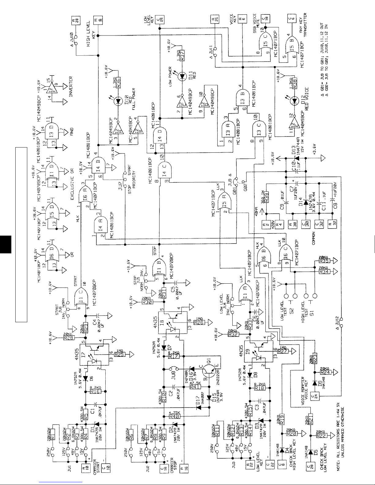
Figure 10–3. TC–10B Keying Schematic. (1606C29).
Page 99

11.1 Transmitter Module
Description
The function of the TC–10B/TCF–10B
Transmitter Module is to provide the RF signal
which drives the 10W PA Module. The
Transmitter’s frequency range is from 30kHz to
535kHz, programmable in 0.1 kHz (100Hz) steps
by four rotary switches on the Transmitter. The
Transmitter is slaved to a crystal oscillator.
The TC–10B/TCF–10B Transmitter Module
operates from keyed inputs (set by jumpers at the
Keying Module):
• High-Level Key
• Any Transmitter Key
•Voice Key
• Shift High (TCF–10B only)
• Shift Low (TCF–10B only)
The Transmitter Module also operates with a
signal from the Optional Voice Adapter Module:
• AM Voice
The Transmitter Module operates with either no
shift (TC-10B) or one of three different frequency
shifts (TCF-10B), selectable by a four-position
dip switch (S5).
11.1.1 Transmitter Control Panel
(This panel is shown in Figure 11-1.)
Operator controls consist of four thumbwheel
switches, representing the frequency range:
Copyright © 2003 Pulsar Technologies, Inc.
Chapter 11. Transmitter Module
11
Schematic 1355D71-8
Parts List 1610C01-11
Group Description
G01 TRANSMITTER
G03 TRANSMITTER W/TTL
Table 11–1. 1610C01 Styles and Descriptions.
Figure 11–1.
Transmitter Module Front Panel.
TRANSMITTER
2
F
R
E
Q
U
5
E
N
C
Y
X
1
0
0
0
H
Z
0
Page 100

• SW1 (x 100kHz)
• SW2 (x 10kHz)
• SW3 (x 1kHz)
• SW4 (x 0.1kHz)
After pulling the module, use a screw driver to set
the thumbwheel switches: CW for higher
frequency, CCW for lower frequency.
11.1.2 Transmitter PC Board
(The Transmitter PC Board is shown in
Figure 11-3.)
Operator controls are as described below.
Potentiometers
R13 Adjusts high-level (10W) output
R12 Adjusts low-level (1W) output
R14 Adjusts voice (4.3W) output level
R1 Adjusts modulation of transmitter
signal (peak-to-valley ratio of signal
envelope)
R29 Sets the offset in output amplifier, so
that when 0dBm is generated, R29 is
adjusted to minimize the 2nd harmonic
distortion
Capacitor
C19 Adjustment for 3.27680MHz clock
oscillator
Switch
S5 No shift used on TC-10B
Test Point
TP1 Clock Oscillator Output
11.2 Transmitter Circuit
Description
The function of the Transmitter Module (see
Figure 11-4, Schematic 1355D71) is to provide
the RF signal (0dBm/.001W, 50Ω balanced),
which drives the 10W PA Module. The
Transmitters frequency range is from 30kHz to
535kHz, programmable in 0.1kHz (100Hz) steps
by four rotary switches on the Transmitter. The
Transmitter Module operates from keyed inputs
(set by jumpers at the Keying Module):
• High-Level (10W) Key (pins C/A-8)
• Any Transmitter Key (pin A-10)
•Voice Key (pins C/A-6)
• Shift High (pin C-10) (TCF–10B Only)
• Shift Low (pins A/C 24) (TCF–10B Only)
The Transmitter Module also operates from an
audio signal from the Optional Voice Adapter
Module: AM Voice (pins C/A-26). Refer to Figure
11-5, Transmitter Block Diagram.
Frequencies are selected using the four BCD
(Binary Coded Decimal) switches (SW1 thru
SW4); the range is from 30.0 to 535.0kHz, in
0.1kHz (100Hz) steps. The 15-bit output of the
BCD switches is converted to a 13-bit binary
number by the BCD-to-Binary converter (ROMs
I1 and I2).
The 13-bit output of ROMs I1 and I2 provides an
input to the Shift and Control Logic (I3), which
consists of three parts:
1. A full adder/subtracter which functions under
control of:
• Shift High (Add)
• Shift Low (Subtract)
2. A frequency-shift, in 50Hz increments from 0
to 750Hz, selected by the 4-position dipswitch (S5).
3. A sequencer and multiplexer (MUX) which
provides the following outputs to the
Numerical Controlled Oscillator (NCO I4):
• Address select (ADDR)
•Write (WRN)
• Load (LDSTB)
•2 (8-bit sequential) data bytes
The NCO (I4) generates digital sine functions of
very precise frequency, to be used in conjunction
with a D/A converter (I5) in analog frequency
Page 11–2 October 2003
TC–10B System Manual
Technologies, Inc.
 Loading...