

Page 1

CPC5565
Intel Core 2 Duo Processor Single Board Computer
User’s Guide
www.pt.com
205 Indigo Creek Drive Rochester, NY 14626 Phone +1.585.256.0200 [email protected]
R
TM
Page 2
Document Revision History
Caution:
Warning:
Date Explanation of changes
December 2, 2009 Initial Production Release
December 10, 2009 Updated default setting in the topic “SW2-4: Console Redirection” on page 38.
January 21, 2010 Updated Table 4-4, “IPMC Sensors,” on page 66
March 24, 2010 Updated Table 4-4, “IPMC Sensors,” on page 66. Updated the command code for
the Get Geographic Address command in Table4-5, “PPS Extension Commands
Supported by the IPMC,” on page 70, and in “Get Geographic Address Command” on
page 76. Updated “Get Status Command” on page71. Added link to the Intel
82571EB NIC in the topic “Ethernet” on page 115.
July 8, 2010 Rebranded and reformatted. Removed reference to hot swap kit for the CPC5565.
August 18, 2010 Updated “Ethernet Interface” on page 4 1 for CPC5565 BIOS version P05.
September 24, 2010 Updated topic “SATA Interface” on pa g e28. Removed all references to SATA drives
on the SODIMM sockets. Updated all references from RTM4810 to RTM4811. Added
Table 3-1, “Default Ethernet Routing,” on page 43. Added the topic “Older Operating
Systems” on page 52. Added driver information to the topic “Ethernet” on page 115.
Copyright Notice
© Copyright 2010 Performance Technologies, Inc. All Rights Reserved.
The PT logo is a registered trademark of Performance Technologies, Inc.
All product and brand names may be trademarks or registered trademarks of their respective owners.
This document is the sole property of Performance Technologies, Inc.
Errors and Omissions
Although diligent efforts are made to supply accurate technical information to the user, occasionally
errors and omissions occur in manuals of this type. Refer to the PT Web site to obtain manual revisions
or current customer information:
http://www.pt.com.
Performance Technologies, Inc., reserves its right to change product specifications without notice.
Symbol Conventions in This Manual
The following symbols appear in this document:
There is risk of equipment damage. Follow the instructions.
Hazardous voltages are present. To reduce the risk of electrical shock and danger to
personal health, follow the instructions.
2
Page 3

Caution:
Electronic components on printed circuit boards are extremely sensitive to static electricity.
Ordinary amounts of static electricity generated by your clothing or work environment can
damage the electronic equipment. It is recommended that anti-static ground straps and antistatic mats are used when installing the board in a system to help prevent damage due to
electrostatic discharge.
Additional safety information is available throughout this guide and in the topic “Product Safety
Information” on page 113.
3
Page 4

4
Page 5

Contents
Chapter 1: About This Guide 15
Text Conventions . . . . . . . . . . . . . . . . . . . . . . . . . . . . . . . . . . . . . . . . . . . . . . . . . . . . . . . . . . . . .16
Customer Support and Services . . . . . . . . . . . . . . . . . . . . . . . . . . . . . . . . . . . . . . . . . . . . . . . . . .16
Customer Support Packages . . . . . . . . . . . . . . . . . . . . . . . . . . . . . . . . . . . . . . . . . . . . . . . . . .17
Other Web Support . . . . . . . . . . . . . . . . . . . . . . . . . . . . . . . . . . . . . . . . . . . . . . . . . . . . . . . . .17
Return Merchandise Authorization (RMA) . . . . . . . . . . . . . . . . . . . . . . . . . . . . . . . . . . . . . . . .17
Product Warranty . . . . . . . . . . . . . . . . . . . . . . . . . . . . . . . . . . . . . . . . . . . . . . . . . . . . . . . . . . . . .17
Chapter 2: Introduction 19
Product Definition . . . . . . . . . . . . . . . . . . . . . . . . . . . . . . . . . . . . . . . . . . . . . . . . . . . . . . . . . . . . .19
CPC5565 Features . . . . . . . . . . . . . . . . . . . . . . . . . . . . . . . . . . . . . . . . . . . . . . . . . . . . . . . . . . . .20
CPC5565 Functional Blocks . . . . . . . . . . . . . . . . . . . . . . . . . . . . . . . . . . . . . . . . . . . . . . . . . . . . .22
Processor . . . . . . . . . . . . . . . . . . . . . . . . . . . . . . . . . . . . . . . . . . . . . . . . . . . . . . . . . . . . . . . .23
Chipset . . . . . . . . . . . . . . . . . . . . . . . . . . . . . . . . . . . . . . . . . . . . . . . . . . . . . . . . . . . . . . . . . .23
CompactPCI Bus Interface . . . . . . . . . . . . . . . . . . . . . . . . . . . . . . . . . . . . . . . . . . . . . . . . . . .24
Intelligent Platform Management Controller . . . . . . . . . . . . . . . . . . . . . . . . . . . . . . . . . . . . . .24
Memory . . . . . . . . . . . . . . . . . . . . . . . . . . . . . . . . . . . . . . . . . . . . . . . . . . . . . . . . . . . . . . . . . .25
Universal Serial Bus (USB) . . . . . . . . . . . . . . . . . . . . . . . . . . . . . . . . . . . . . . . . . . . . . . . . . . .25
AMD/ATI Radeon E2400 Video Processor . . . . . . . . . . . . . . . . . . . . . . . . . . . . . . . . . . . . . . .25
Video Features . . . . . . . . . . . . . . . . . . . . . . . . . . . . . . . . . . . . . . . . . . . . . . . . . . . . . . . . .26
SMARTSHADER 4.0 - Advanced Shader Technology . . . . . . . . . . . . . . . . . . . . . . . . . . .26
SMOOTHVISION 2.0 - Flexible Anti-Aliasing and Anisotropic Filtering . . . . . . . . . . . . . .26
Avivo™ Display Support - Two Fully Functional Displays . . . . . . . . . . . . . . . . . . . . . . . . .26
Video Acceleration . . . . . . . . . . . . . . . . . . . . . . . . . . . . . . . . . . . . . . . . . . . . . . . . . . . . . . .27
Serial I/O . . . . . . . . . . . . . . . . . . . . . . . . . . . . . . . . . . . . . . . . . . . . . . . . . . . . . . . . . . . . . . . . .27
Ethernet Interface . . . . . . . . . . . . . . . . . . . . . . . . . . . . . . . . . . . . . . . . . . . . . . . . . . . . . . . . . .27
SATA Interface . . . . . . . . . . . . . . . . . . . . . . . . . . . . . . . . . . . . . . . . . . . . . . . . . . . . . . . . . . . .28
Rear Transition Module (Optional) . . . . . . . . . . . . . . . . . . . . . . . . . . . . . . . . . . . . . . . . . . . . .28
PTMC Interface (Build Option) . . . . . . . . . . . . . . . . . . . . . . . . . . . . . . . . . . . . . . . . . . . . . . . .28
Drone Mode . . . . . . . . . . . . . . . . . . . . . . . . . . . . . . . . . . . . . . . . . . . . . . . . . . . . . . . . . . . . . . .29
5
Page 6

Contents
Real-Time Clock, CMOS RAM and Battery . . . . . . . . . . . . . . . . . . . . . . . . . . . . . . . . . . . . . . 29
Reset . . . . . . . . . . . . . . . . . . . . . . . . . . . . . . . . . . . . . . . . . . . . . . . . . . . . . . . . . . . . . . . . . . . 30
Two-Stage Watchdog Timer . . . . . . . . . . . . . . . . . . . . . . . . . . . . . . . . . . . . . . . . . . . . . . . . . . 30
LED Indicators . . . . . . . . . . . . . . . . . . . . . . . . . . . . . . . . . . . . . . . . . . . . . . . . . . . . . . . . . . . . 30
User LED . . . . . . . . . . . . . . . . . . . . . . . . . . . . . . . . . . . . . . . . . . . . . . . . . . . . . . . . . . . . . 30
Front Panel Ethernet (RJ-45 Connector) . . . . . . . . . . . . . . . . . . . . . . . . . . . . . . . . . . . . . 30
Hot Swap . . . . . . . . . . . . . . . . . . . . . . . . . . . . . . . . . . . . . . . . . . . . . . . . . . . . . . . . . . . . . 31
Status/Health . . . . . . . . . . . . . . . . . . . . . . . . . . . . . . . . . . . . . . . . . . . . . . . . . . . . . . . . . . 31
Rear-Panel I/O . . . . . . . . . . . . . . . . . . . . . . . . . . . . . . . . . . . . . . . . . . . . . . . . . . . . . . . . . . . . 31
Software . . . . . . . . . . . . . . . . . . . . . . . . . . . . . . . . . . . . . . . . . . . . . . . . . . . . . . . . . . . . . . . . . . . . 31
BIOS . . . . . . . . . . . . . . . . . . . . . . . . . . . . . . . . . . . . . . . . . . . . . . . . . . . . . . . . . . . . . . . . . . . . 31
Operating Systems Supported . . . . . . . . . . . . . . . . . . . . . . . . . . . . . . . . . . . . . . . . . . . . . . . . 32
IPMI . . . . . . . . . . . . . . . . . . . . . . . . . . . . . . . . . . . . . . . . . . . . . . . . . . . . . . . . . . . . . . . . . . . . 32
Chapter 3: Getting Started 33
Unpacking . . . . . . . . . . . . . . . . . . . . . . . . . . . . . . . . . . . . . . . . . . . . . . . . . . . . . . . . . . . . . . . . . . 34
Electrical and Environmental Requirements . . . . . . . . . . . . . . . . . . . . . . . . . . . . . . . . . . . . . . . . 34
Memory Configuration . . . . . . . . . . . . . . . . . . . . . . . . . . . . . . . . . . . . . . . . . . . . . . . . . . . . . . . . . 34
I/O Configuration . . . . . . . . . . . . . . . . . . . . . . . . . . . . . . . . . . . . . . . . . . . . . . . . . . . . . . . . . . . . . 36
Connectivity . . . . . . . . . . . . . . . . . . . . . . . . . . . . . . . . . . . . . . . . . . . . . . . . . . . . . . . . . . . . . . . . . 37
Switches . . . . . . . . . . . . . . . . . . . . . . . . . . . . . . . . . . . . . . . . . . . . . . . . . . . . . . . . . . . . . . . . . . . . 37
Switch Pack 1 (SW1) . . . . . . . . . . . . . . . . . . . . . . . . . . . . . . . . . . . . . . . . . . . . . . . . . . . . . . . 37
SW1-1: PCIXCAP Override on Local PCI Bus . . . . . . . . . . . . . . . . . . . . . . . . . . . . . . . . . 37
SW1-2: COM Port Override . . . . . . . . . . . . . . . . . . . . . . . . . . . . . . . . . . . . . . . . . . . . . . . 38
SW1-3: IPMC JTAG Selection . . . . . . . . . . . . . . . . . . . . . . . . . . . . . . . . . . . . . . . . . . . . . 38
SW1-4: Drone Reset Control . . . . . . . . . . . . . . . . . . . . . . . . . . . . . . . . . . . . . . . . . . . . . . 38
Switch Pack 2 (SW2) . . . . . . . . . . . . . . . . . . . . . . . . . . . . . . . . . . . . . . . . . . . . . . . . . . . . . . . 38
SW2-1: Clear CMOS . . . . . . . . . . . . . . . . . . . . . . . . . . . . . . . . . . . . . . . . . . . . . . . . . . . . 38
SW2-2, SW2-3: User Switch Bits . . . . . . . . . . . . . . . . . . . . . . . . . . . . . . . . . . . . . . . . . . . 38
SW2-4: Console Redirection . . . . . . . . . . . . . . . . . . . . . . . . . . . . . . . . . . . . . . . . . . . . . . 38
Switch Pack 3 (SW3) . . . . . . . . . . . . . . . . . . . . . . . . . . . . . . . . . . . . . . . . . . . . . . . . . . . . . . . 39
SW3-1 Port 80 Post Codes Out Serial Port (Front Panel) . . . . . . . . . . . . . . . . . . . . . . . . 39
SW3-2 Reserved . . . . . . . . . . . . . . . . . . . . . . . . . . . . . . . . . . . . . . . . . . . . . . . . . . . . . . . 39
SW3-3 Force Drone Mode . . . . . . . . . . . . . . . . . . . . . . . . . . . . . . . . . . . . . . . . . . . . . . . . 39
SW3-4 Reserved . . . . . . . . . . . . . . . . . . . . . . . . . . . . . . . . . . . . . . . . . . . . . . . . . . . . . . . 39
Push-Button Reset (SW4) . . . . . . . . . . . . . . . . . . . . . . . . . . . . . . . . . . . . . . . . . . . . . . . . . . . 39
6
Page 7

Contents
Hot-Swap Switch (SW5) . . . . . . . . . . . . . . . . . . . . . . . . . . . . . . . . . . . . . . . . . . . . . . . . . . . . .39
BIOS Configuration Overview . . . . . . . . . . . . . . . . . . . . . . . . . . . . . . . . . . . . . . . . . . . . . . . . . . . .40
Ethernet Interface . . . . . . . . . . . . . . . . . . . . . . . . . . . . . . . . . . . . . . . . . . . . . . . . . . . . . . . . . .41
Ethernet Switch BIOS Options . . . . . . . . . . . . . . . . . . . . . . . . . . . . . . . . . . . . . . . . . . . . .42
VLAN Configuration . . . . . . . . . . . . . . . . . . . . . . . . . . . . . . . . . . . . . . . . . . . . . . . . . . . . . .42
VLAN Configurations . . . . . . . . . . . . . . . . . . . . . . . . . . . . . . . . . . . . . . . . . . . . . . . . . . . . . . . . .42
Jumbo Frames Configuration . . . . . . . . . . . . . . . . . . . . . . . . . . . . . . . . . . . . . . . . . . . . . .45
Port Trunking Configuration . . . . . . . . . . . . . . . . . . . . . . . . . . . . . . . . . . . . . . . . . . . . . . . .46
MAC Address Handling Configuration . . . . . . . . . . . . . . . . . . . . . . . . . . . . . . . . . . . . . . . .47
Network Architecture Considerations . . . . . . . . . . . . . . . . . . . . . . . . . . . . . . . . . . . . . . . .48
Avoiding Loops . . . . . . . . . . . . . . . . . . . . . . . . . . . . . . . . . . . . . . . . . . . . . . . . . . . . . . . . . . . . .48
Console Redirection . . . . . . . . . . . . . . . . . . . . . . . . . . . . . . . . . . . . . . . . . . . . . . . . . . . . . . . .52
Older Operating Systems . . . . . . . . . . . . . . . . . . . . . . . . . . . . . . . . . . . . . . . . . . . . . . . . . . . .52
Custom Default Setup . . . . . . . . . . . . . . . . . . . . . . . . . . . . . . . . . . . . . . . . . . . . . . . . . . . . . . .53
Behavior of the BIOS if a Corrupted CMOS Checksum is Detected . . . . . . . . . . . . . . . . .53
Installing a PMC Device . . . . . . . . . . . . . . . . . . . . . . . . . . . . . . . . . . . . . . . . . . . . . . . . . . . . . . . .54
Installing the Operating System . . . . . . . . . . . . . . . . . . . . . . . . . . . . . . . . . . . . . . . . . . . . . . . . . .57
USB CD/DVD . . . . . . . . . . . . . . . . . . . . . . . . . . . . . . . . . . . . . . . . . . . . . . . . . . . . . . . . . . . . .57
PXE . . . . . . . . . . . . . . . . . . . . . . . . . . . . . . . . . . . . . . . . . . . . . . . . . . . . . . . . . . . . . . . . . . . . .58
Operating Systems Supported . . . . . . . . . . . . . . . . . . . . . . . . . . . . . . . . . . . . . . . . . . . . . . . .58
Programming the LEDS . . . . . . . . . . . . . . . . . . . . . . . . . . . . . . . . . . . . . . . . . . . . . . . . . . . . . . . .59
Installing the Display Drivers . . . . . . . . . . . . . . . . . . . . . . . . . . . . . . . . . . . . . . . . . . . . . . . . . . . . .59
Windows XP (32- and 64-Bit Editions) . . . . . . . . . . . . . . . . . . . . . . . . . . . . . . . . . . . . . . . . . .60
Linux . . . . . . . . . . . . . . . . . . . . . . . . . . . . . . . . . . . . . . . . . . . . . . . . . . . . . . . . . . . . . . . . . . . .60
Solaris . . . . . . . . . . . . . . . . . . . . . . . . . . . . . . . . . . . . . . . . . . . . . . . . . . . . . . . . . . . . . . . . . . .60
Chapter 4: System Monitoring and Alarms 61
IPMC Functions . . . . . . . . . . . . . . . . . . . . . . . . . . . . . . . . . . . . . . . . . . . . . . . . . . . . . . . . . . . . . . .61
Summary of Supported Commands . . . . . . . . . . . . . . . . . . . . . . . . . . . . . . . . . . . . . . . . . . . . . . .62
Device Locator Record . . . . . . . . . . . . . . . . . . . . . . . . . . . . . . . . . . . . . . . . . . . . . . . . . . . . . . . . .64
Device ID . . . . . . . . . . . . . . . . . . . . . . . . . . . . . . . . . . . . . . . . . . . . . . . . . . . . . . . . . . . . . . . . .65
Sensors . . . . . . . . . . . . . . . . . . . . . . . . . . . . . . . . . . . . . . . . . . . . . . . . . . . . . . . . . . . . . . . . . . . . .66
Interpreting Sensor Events . . . . . . . . . . . . . . . . . . . . . . . . . . . . . . . . . . . . . . . . . . . . . . . . . . .67
Serial Interface Subsystem . . . . . . . . . . . . . . . . . . . . . . . . . . . . . . . . . . . . . . . . . . . . . . . . . . . . . .68
Terminal Mode Messages and Commands . . . . . . . . . . . . . . . . . . . . . . . . . . . . . . . . . . . . . . .68
Terminal Mode Message Format . . . . . . . . . . . . . . . . . . . . . . . . . . . . . . . . . . . . . . . . . . . .68
7
Page 8

Contents
Raw IPMI Messages . . . . . . . . . . . . . . . . . . . . . . . . . . . . . . . . . . . . . . . . . . . . . . . . . . . . . 68
Terminal Mode Text Commands . . . . . . . . . . . . . . . . . . . . . . . . . . . . . . . . . . . . . . . . . . . 68
Pigeon Point Systems (PPS) Extension Commands . . . . . . . . . . . . . . . . . . . . . . . . . . . . 69
Terminal Mode Line Editing . . . . . . . . . . . . . . . . . . . . . . . . . . . . . . . . . . . . . . . . . . . . . . . . . . 69
Supported PPS Extension Commands . . . . . . . . . . . . . . . . . . . . . . . . . . . . . . . . . . . . . . . . . . 70
Get Status Command . . . . . . . . . . . . . . . . . . . . . . . . . . . . . . . . . . . . . . . . . . . . . . . . . . . . 71
Serial Line Properties Commands . . . . . . . . . . . . . . . . . . . . . . . . . . . . . . . . . . . . . . . . . . 72
Get Serial Interface Properties Command . . . . . . . . . . . . . . . . . . . . . . . . . . . . . . . . . . . . . . . . 72
Set Serial Interface Properties Command . . . . . . . . . . . . . . . . . . . . . . . . . . . . . . . . . . . . . . . . 72
Debug/Verbosity Level . . . . . . . . . . . . . . . . . . . . . . . . . . . . . . . . . . . . . . . . . . . . . . . . . . . 73
Get Debug Level Command . . . . . . . . . . . . . . . . . . . . . . . . . . . . . . . . . . . . . . . . . . . . . . . . . . . 73
Set Debug Level Command . . . . . . . . . . . . . . . . . . . . . . . . . . . . . . . . . . . . . . . . . . . . . . . . . . .73
Payload Communication Timeout . . . . . . . . . . . . . . . . . . . . . . . . . . . . . . . . . . . . . . . . . . . 74
Get Payload Communication Timeout Command . . . . . . . . . . . . . . . . . . . . . . . . . . . . . . . . . . . 74
Set Payload Communication Timeout Command . . . . . . . . . . . . . . . . . . . . . . . . . . . . . . . . . . . 74
Graceful Payload Reset . . . . . . . . . . . . . . . . . . . . . . . . . . . . . . . . . . . . . . . . . . . . . . . . . . 74
Payload Diagnostic Interrupt . . . . . . . . . . . . . . . . . . . . . . . . . . . . . . . . . . . . . . . . . . . . . . 75
Payload Shutdown Timeout . . . . . . . . . . . . . . . . . . . . . . . . . . . . . . . . . . . . . . . . . . . . . . . 75
Get Payload Shutdown Timeout Command . . . . . . . . . . . . . . . . . . . . . . . . . . . . . . . . . . . . . . . 75
Set Payload Shutdown Timeout Command . . . . . . . . . . . . . . . . . . . . . . . . . . . . . . . . . . . . . . . 76
Get Geographic Address Command . . . . . . . . . . . . . . . . . . . . . . . . . . . . . . . . . . . . . . . . 76
Firmware Upgrade Process . . . . . . . . . . . . . . . . . . . . . . . . . . . . . . . . . . . . . . . . . . . . . . . . . . . . . 76
HPM.1 Boot Loader . . . . . . . . . . . . . . . . . . . . . . . . . . . . . . . . . . . . . . . . . . . . . . . . . . . . . . . . 76
HPM.1 Firmware Upgrade . . . . . . . . . . . . . . . . . . . . . . . . . . . . . . . . . . . . . . . . . . . . . . . . . . . 77
Upgrade Utilities . . . . . . . . . . . . . . . . . . . . . . . . . . . . . . . . . . . . . . . . . . . . . . . . . . . . . . . . . . . 77
Detailed HPM.1 Upgrade Procedure . . . . . . . . . . . . . . . . . . . . . . . . . . . . . . . . . . . . . . . . . . . 78
IPMI Communication Utility (ipmitool) . . . . . . . . . . . . . . . . . . . . . . . . . . . . . . . . . . . . . . . . . . . 78
Building the ipmitool Utility . . . . . . . . . . . . . . . . . . . . . . . . . . . . . . . . . . . . . . . . . . . . . . . . 79
Accessing an IPMC with ipmitool . . . . . . . . . . . . . . . . . . . . . . . . . . . . . . . . . . . . . . . . . . . 79
Accessing an IPMC via a Shelf Manager . . . . . . . . . . . . . . . . . . . . . . . . . . . . . . . . . . . . . . . . . 79
Accessing an IPMC via a Serial Interface . . . . . . . . . . . . . . . . . . . . . . . . . . . . . . . . . . . . . . . . . 80
Using ipmitool for HPM.1 Upgrades . . . . . . . . . . . . . . . . . . . . . . . . . . . . . . . . . . . . . . . . . 80
HPM.1 Commands . . . . . . . . . . . . . . . . . . . . . . . . . . . . . . . . . . . . . . . . . . . . . . . . . . . . . . 80
targetcap . . . . . . . . . . . . . . . . . . . . . . . . . . . . . . . . . . . . . . . . . . . . . . . . . . . . . . . . . . . . . . . . . . 81
compprop . . . . . . . . . . . . . . . . . . . . . . . . . . . . . . . . . . . . . . . . . . . . . . . . . . . . . . . . . . . . . . . . . 82
upgrade . . . . . . . . . . . . . . . . . . . . . . . . . . . . . . . . . . . . . . . . . . . . . . . . . . . . . . . . . . . . . . . . . . . 82
activate . . . . . . . . . . . . . . . . . . . . . . . . . . . . . . . . . . . . . . . . . . . . . . . . . . . . . . . . . . . . . . . . . . .83
rollback . . . . . . . . . . . . . . . . . . . . . . . . . . . . . . . . . . . . . . . . . . . . . . . . . . . . . . . . . . . . . . . . . . .83
rollbackstatus . . . . . . . . . . . . . . . . . . . . . . . . . . . . . . . . . . . . . . . . . . . . . . . . . . . . . . . . . . . . . . 83
8
Page 9

Contents
Chapter 5: Connectors 85
Backplane Connectors . . . . . . . . . . . . . . . . . . . . . . . . . . . . . . . . . . . . . . . . . . . . . . . . . . . . . . . . .87
J1 (IPMB/Power Connector) . . . . . . . . . . . . . . . . . . . . . . . . . . . . . . . . . . . . . . . . . . . . . . . . . .87
J2 (V(I/O) Connector) . . . . . . . . . . . . . . . . . . . . . . . . . . . . . . . . . . . . . . . . . . . . . . . . . . . . . . .88
J3 (Rear-Panel Gigabit Ethernet Connector) . . . . . . . . . . . . . . . . . . . . . . . . . . . . . . . . . . . . . .89
J5 (Rear-Panel User I/O Connector) . . . . . . . . . . . . . . . . . . . . . . . . . . . . . . . . . . . . . . . . . . . .90
Front Panel Connectors . . . . . . . . . . . . . . . . . . . . . . . . . . . . . . . . . . . . . . . . . . . . . . . . . . . . . . . .90
DVI-I Connector (J6) . . . . . . . . . . . . . . . . . . . . . . . . . . . . . . . . . . . . . . . . . . . . . . . . . . . . . . . .91
RS-232 RJ-45 Console Port (J7) . . . . . . . . . . . . . . . . . . . . . . . . . . . . . . . . . . . . . . . . . . . . . . .92
Ethernet Connectors (J8 and J9) . . . . . . . . . . . . . . . . . . . . . . . . . . . . . . . . . . . . . . . . . . . . . . .92
USB Connectors (J10, J15) . . . . . . . . . . . . . . . . . . . . . . . . . . . . . . . . . . . . . . . . . . . . . . . . . . .93
Internal Connectors . . . . . . . . . . . . . . . . . . . . . . . . . . . . . . . . . . . . . . . . . . . . . . . . . . . . . . . . . . . .93
PTMC Connectors (J11, J12, J13, and J14) (Optional) . . . . . . . . . . . . . . . . . . . . . . . . . . . . . .93
DDR2 SDRAM Connectors (P1, P2) . . . . . . . . . . . . . . . . . . . . . . . . . . . . . . . . . . . . . . . . . . . .98
Hot-Swap Ejector Switch Connector (P3) . . . . . . . . . . . . . . . . . . . . . . . . . . . . . . . . . . . . . . . .98
SATA Hard Disk Connector (Optional) . . . . . . . . . . . . . . . . . . . . . . . . . . . . . . . . . . . . . . . . . .98
Cables . . . . . . . . . . . . . . . . . . . . . . . . . . . . . . . . . . . . . . . . . . . . . . . . . . . . . . . . . . . . . . . . . . . . . .99
Serial Cables . . . . . . . . . . . . . . . . . . . . . . . . . . . . . . . . . . . . . . . . . . . . . . . . . . . . . . . . . . . . . .99
Chapter 6: Reset 101
Reset Types and Sources . . . . . . . . . . . . . . . . . . . . . . . . . . . . . . . . . . . . . . . . . . . . . . . . . . . . . .101
General Reset Sources . . . . . . . . . . . . . . . . . . . . . . . . . . . . . . . . . . . . . . . . . . . . . . . . . . . . .101
Push-Button Reset . . . . . . . . . . . . . . . . . . . . . . . . . . . . . . . . . . . . . . . . . . . . . . . . . . . . .101
NMI\SMI\SERIRQ Sources . . . . . . . . . . . . . . . . . . . . . . . . . . . . . . . . . . . . . . . . . . . . . . . . . .101
Watchdog Timer . . . . . . . . . . . . . . . . . . . . . . . . . . . . . . . . . . . . . . . . . . . . . . . . . . . . . . .101
Chapter 7: Specifications 103
Electrical and Environmental Specifications . . . . . . . . . . . . . . . . . . . . . . . . . . . . . . . . . . . . . . . .103
CPC5565 Absolute Maximum Ratings . . . . . . . . . . . . . . . . . . . . . . . . . . . . . . . . . . . . . . . . .103
Operating Temperature . . . . . . . . . . . . . . . . . . . . . . . . . . . . . . . . . . . . . . . . . . . . . . . . . .103
DC Operating Characteristics . . . . . . . . . . . . . . . . . . . . . . . . . . . . . . . . . . . . . . . . . . . . . . . .104
Power Consumption with 2.2 GHz Processor . . . . . . . . . . . . . . . . . . . . . . . . . . . . . . . . .104
Maximum Available Current for PMC Module . . . . . . . . . . . . . . . . . . . . . . . . . . . . . . . . .105
Battery Backup Characteristics . . . . . . . . . . . . . . . . . . . . . . . . . . . . . . . . . . . . . . . . . . . . . . .105
Battery Replacement . . . . . . . . . . . . . . . . . . . . . . . . . . . . . . . . . . . . . . . . . . . . . . . . . . . .105
9
Page 10

Contents
CPC5565 Reliability . . . . . . . . . . . . . . . . . . . . . . . . . . . . . . . . . . . . . . . . . . . . . . . . . . . . . . . . . . 106
Mechanical Specifications . . . . . . . . . . . . . . . . . . . . . . . . . . . . . . . . . . . . . . . . . . . . . . . . . . . . . 107
CPC5565 Connectors . . . . . . . . . . . . . . . . . . . . . . . . . . . . . . . . . . . . . . . . . . . . . . . . . . . . . . 107
Chapter 8: Thermal Considerations 109
Thermal Requirements . . . . . . . . . . . . . . . . . . . . . . . . . . . . . . . . . . . . . . . . . . . . . . . . . . . . . . . . 109
Temperature Monitoring . . . . . . . . . . . . . . . . . . . . . . . . . . . . . . . . . . . . . . . . . . . . . . . . . . . . . . . 109
Intel Thermal Monitor . . . . . . . . . . . . . . . . . . . . . . . . . . . . . . . . . . . . . . . . . . . . . . . . . . . . . . 109
Chapter 9: Agency Approvals 111
CE Certification . . . . . . . . . . . . . . . . . . . . . . . . . . . . . . . . . . . . . . . . . . . . . . . . . . . . . . . . . . . . . 111
Safety . . . . . . . . . . . . . . . . . . . . . . . . . . . . . . . . . . . . . . . . . . . . . . . . . . . . . . . . . . . . . . . . . . . . . 111
Emissions Test Regulations . . . . . . . . . . . . . . . . . . . . . . . . . . . . . . . . . . . . . . . . . . . . . . . . . . . . 111
EN 50081-1 Emissions . . . . . . . . . . . . . . . . . . . . . . . . . . . . . . . . . . . . . . . . . . . . . . . . . . . . . 111
EN 55024 Immunity . . . . . . . . . . . . . . . . . . . . . . . . . . . . . . . . . . . . . . . . . . . . . . . . . . . . . . . 112
Regulatory Information . . . . . . . . . . . . . . . . . . . . . . . . . . . . . . . . . . . . . . . . . . . . . . . . . . . . . . . . 112
FCC (USA) . . . . . . . . . . . . . . . . . . . . . . . . . . . . . . . . . . . . . . . . . . . . . . . . . . . . . . . . . . . . . . 112
Industry Canada (Canada) . . . . . . . . . . . . . . . . . . . . . . . . . . . . . . . . . . . . . . . . . . . . . . . . . . 112
Product Safety Information . . . . . . . . . . . . . . . . . . . . . . . . . . . . . . . . . . . . . . . . . . . . . . . . . . . . . 113
Safety Precautions . . . . . . . . . . . . . . . . . . . . . . . . . . . . . . . . . . . . . . . . . . . . . . . . . . . . . . . . 113
Compliance with RoHS and WEEE Directives . . . . . . . . . . . . . . . . . . . . . . . . . . . . . . . . . . . . . . 114
Chapter 10: Data Sheet Reference 115
AMD/ATI Radeon E2400 Video Processor . . . . . . . . . . . . . . . . . . . . . . . . . . . . . . . . . . . . . . . . 115
Chipset . . . . . . . . . . . . . . . . . . . . . . . . . . . . . . . . . . . . . . . . . . . . . . . . . . . . . . . . . . . . . . . . . . . . 115
Ethernet . . . . . . . . . . . . . . . . . . . . . . . . . . . . . . . . . . . . . . . . . . . . . . . . . . . . . . . . . . . . . . . . . . . 115
Intelligent Platform Management Controller . . . . . . . . . . . . . . . . . . . . . . . . . . . . . . . . . . . . . . . . 116
I/O Controller . . . . . . . . . . . . . . . . . . . . . . . . . . . . . . . . . . . . . . . . . . . . . . . . . . . . . . . . . . . . . . . 116
PICMG Specifications . . . . . . . . . . . . . . . . . . . . . . . . . . . . . . . . . . . . . . . . . . . . . . . . . . . . . . . . 116
Processor . . . . . . . . . . . . . . . . . . . . . . . . . . . . . . . . . . . . . . . . . . . . . . . . . . . . . . . . . . . . . . . . . . 117
User Documentation . . . . . . . . . . . . . . . . . . . . . . . . . . . . . . . . . . . . . . . . . . . . . . . . . . . . . . . . . . 117
10
Page 11

Tables
Table 3-1: Default Ethernet Routing. . . . . . . . . . . . . . . . . . . . . . . . . . . . . . . . . . . . . . . . . . . . . . . . . . 43
Table 4-1: IPMI/PICMG Command Subset Supported by the IPMC Firmware . . . . . . . . . . . . . . . . . 62
Table 4-2: IPMB Management Controller Device Locator Record. . . . . . . . . . . . . . . . . . . . . . . . . . . 64
Table 4-3: IPMC Device ID. . . . . . . . . . . . . . . . . . . . . . . . . . . . . . . . . . . . . . . . . . . . . . . . . . . . . . . . . 65
Table 4-4: IPMC Sensors. . . . . . . . . . . . . . . . . . . . . . . . . . . . . . . . . . . . . . . . . . . . . . . . . . . . . . . . . . 66
Table 4-5: PPS Extension Commands Supported by the IPMC . . . . . . . . . . . . . . . . . . . . . . . . . . . . 70
Table 4-6: IPMC Status Bits. . . . . . . . . . . . . . . . . . . . . . . . . . . . . . . . . . . . . . . . . . . . . . . . . . . . . . . . 71
Table 4-7: The <interface ID> Parameter Values. . . . . . . . . . . . . . . . . . . . . . . . . . . . . . . . . . . . . . . . 72
Table 4-8: The <interface properties> Parameter Bit Fields . . . . . . . . . . . . . . . . . . . . . . . . . . . . . . . 72
Table 4-9: IPMC Debug Levels . . . . . . . . . . . . . . . . . . . . . . . . . . . . . . . . . . . . . . . . . . . . . . . . . . . . . 73
Table 5-1: Connector Assignments . . . . . . . . . . . . . . . . . . . . . . . . . . . . . . . . . . . . . . . . . . . . . . . . . . 85
Table 5-2: J1 CompactPCI Bus Connector Pinout. . . . . . . . . . . . . . . . . . . . . . . . . . . . . . . . . . . . . . . 87
Table 5-3: J2 V(I/O) Connector Pinout. . . . . . . . . . . . . . . . . . . . . . . . . . . . . . . . . . . . . . . . . . . . . . . . 88
Table 5-4: J3 Rear-Panel Gigabit Ethernet Connector Pinout. . . . . . . . . . . . . . . . . . . . . . . . . . . . . . 89
Table 5-5: J5 Rear-Panel User I/O Connector Pinout . . . . . . . . . . . . . . . . . . . . . . . . . . . . . . . . . . . . 90
Table 5-6: DVI-I Connector J6 Pinout . . . . . . . . . . . . . . . . . . . . . . . . . . . . . . . . . . . . . . . . . . . . . . . . 91
Table 5-7: RJ-45 Console Port J7 Pinout. . . . . . . . . . . . . . . . . . . . . . . . . . . . . . . . . . . . . . . . . . . . . . 92
Table 5-8: Ethernet Connectors J8 and J9 Pinout. . . . . . . . . . . . . . . . . . . . . . . . . . . . . . . . . . . . . . . 92
Table 5-9: USB Connectors J10, J15 Pinout . . . . . . . . . . . . . . . . . . . . . . . . . . . . . . . . . . . . . . . . . . . 93
Table 5-10: PTMC Connector J11 Pinout . . . . . . . . . . . . . . . . . . . . . . . . . . . . . . . . . . . . . . . . . . . . . 94
Table 5-11: PTMC Connector Pin Map (J12). . . . . . . . . . . . . . . . . . . . . . . . . . . . . . . . . . . . . . . . . . . 95
Table 5-12: PTMC Connector Pin Map (J13). . . . . . . . . . . . . . . . . . . . . . . . . . . . . . . . . . . . . . . . . . . 96
11
Page 12

Tables
Table 5-13: PTMC Connector Pin Map (J14) . . . . . . . . . . . . . . . . . . . . . . . . . . . . . . . . . . . . . . . . . . . 97
Table 5-14: P3 Hot-Swap Ejector Switch Connector Pinout . . . . . . . . . . . . . . . . . . . . . . . . . . . . . . . . 98
Table 5-15: Management Cable Pinout. . . . . . . . . . . . . . . . . . . . . . . . . . . . . . . . . . . . . . . . . . . . . . . . 99
Table 7-1: Power Consumption with 2.2 GHz Processor . . . . . . . . . . . . . . . . . . . . . . . . . . . . . . . . . 104
12
Page 13

Figures
Figure 2-1: CPC5565 Front Panel . . . . . . . . . . . . . . . . . . . . . . . . . . . . . . . . . . . . . . . . . . . . . . . . . . . 19
Figure 2-2: CPC5565 Functional Block Diagram. . . . . . . . . . . . . . . . . . . . . . . . . . . . . . . . . . . . . . . . 22
Figure 3-1: Memory Address Map Example. . . . . . . . . . . . . . . . . . . . . . . . . . . . . . . . . . . . . . . . . . . . 35
Figure 3-2: I/O Address Map . . . . . . . . . . . . . . . . . . . . . . . . . . . . . . . . . . . . . . . . . . . . . . . . . . . . . . . 36
Figure 3-3: Switch Locations . . . . . . . . . . . . . . . . . . . . . . . . . . . . . . . . . . . . . . . . . . . . . . . . . . . . . . . 37
Figure 3-4: Setup Screen Layout. . . . . . . . . . . . . . . . . . . . . . . . . . . . . . . . . . . . . . . . . . . . . . . . . . . . 40
Figure 3-5: Switch Configuration Screen . . . . . . . . . . . . . . . . . . . . . . . . . . . . . . . . . . . . . . . . . . . . . . 42
Figure 3-6: VLAN Configuration Screen. . . . . . . . . . . . . . . . . . . . . . . . . . . . . . . . . . . . . . . . . . . . . . . 43
Figure 3-7: Jumbo Frames Configuration Screen . . . . . . . . . . . . . . . . . . . . . . . . . . . . . . . . . . . . . . . 45
Figure 3-8: Port Trunking Configuration Screen. . . . . . . . . . . . . . . . . . . . . . . . . . . . . . . . . . . . . . . . . 46
Figure 3-9: MAC Address Handling Configuration Screen. . . . . . . . . . . . . . . . . . . . . . . . . . . . . . . . . 47
Figure 3-10: Inter-Switch Link Connection. . . . . . . . . . . . . . . . . . . . . . . . . . . . . . . . . . . . . . . . . . . . . 48
Figure 3-11: Separate Switching Domains. . . . . . . . . . . . . . . . . . . . . . . . . . . . . . . . . . . . . . . . . . . . . 49
Figure 3-12: ISL Segregation and MAC Address Learning . . . . . . . . . . . . . . . . . . . . . . . . . . . . . . . . 50
Figure 3-13: Spanning Tree Redundancy . . . . . . . . . . . . . . . . . . . . . . . . . . . . . . . . . . . . . . . . . . . . . 51
Figure 3-14: Saving Custom Defaults . . . . . . . . . . . . . . . . . . . . . . . . . . . . . . . . . . . . . . . . . . . . . . . . 53
Figure 3-15: Solder-Side Shield. . . . . . . . . . . . . . . . . . . . . . . . . . . . . . . . . . . . . . . . . . . . . . . . . . . . . 54
Figure 3-16: PMC Card Installation . . . . . . . . . . . . . . . . . . . . . . . . . . . . . . . . . . . . . . . . . . . . . . . . . . 56
Figure 4-1: PPS Extension Command Request. . . . . . . . . . . . . . . . . . . . . . . . . . . . . . . . . . . . . . . . . 69
Figure 4-2: PPS Extension Command Response . . . . . . . . . . . . . . . . . . . . . . . . . . . . . . . . . . . . . . . 69
Figure 5-1: Connector Locations . . . . . . . . . . . . . . . . . . . . . . . . . . . . . . . . . . . . . . . . . . . . . . . . . . . . 86
Figure 5-2: Backplane Connectors Pin Locations . . . . . . . . . . . . . . . . . . . . . . . . . . . . . . . . . . . . . . . 86
13
Page 14

Figures
Figure 7-1: Battery Socket Locations . . . . . . . . . . . . . . . . . . . . . . . . . . . . . . . . . . . . . . . . . . . . . . . . 106
Figure 7-2: CPC5565 Board Dimensions . . . . . . . . . . . . . . . . . . . . . . . . . . . . . . . . . . . . . . . . . . . . . 107
14
Page 15

Chapter 1
About This Guide
This manual describes the operation and use of the CPC5565 Intel® Core™ 2 Duo Single
Board Computer (referred to as the CPC5565 in this guide). The following outline describes the
focus of each chapter.
Chapter 2, “Introduction,” on page 19 provides an overview of the CPC5565 and includes
information such as product features, a functional block diagram with a brief description of each
block, and descriptions of software such as the BIOS, supported operating systems, and IPMI.
Chapter 3, “Getting Started,” on page 33 provides setup information such as unpacking the
product, system requirements, and installation procedures.
Chapter 4, “System Monitoring and Alarms,” on page 61 describes the commands supported
by the on-board Intelligent Platform Management Controller.
Chapter 5, “Connectors,” on page 85 provides connector location, description, and pinout
information for the CPC5565’s CompactPCI connectors, fro nt panel, and internal connecto rs. It
also includes a description of the serial cable recommended for use with the front panel RJ11
serial connector.
Chapter 6, “Reset,” on page 101 describes the CPC5565 reset types with their respective
sources.
Chapter 7, “Specifications,” on page 103 contains mechanical, electrical, and environmental
specifications as well as product reliability specifications.
Chapter 8, “Thermal Considerations,” on page 109 describes the thermal requirements to
reliably operate a CPC5565 processor board.
Chapter 9, “Agency Approvals,” on page 111 presents agency approval and certification
information.
Chapter 10, “Data Sheet Reference,” on page 115 provides information on data sheets,
standards, and specifications for the technology designed into the CPC5565.
The CPC5565 assembly should be used in conjunction with the PT software package that you
have chosen, for example NexusWare
The most current documentation to support any additional components that you purchased
from PT is available at www.pt.com under the product you are inquiring about.
For additional documentation references see Chapter 10, “Data Sheet Reference,” on
page 115.
®
Core.
15
Page 16

Chapter 1: About This Guide
Text Conventions
Conventions in This Guide describes the text conventions that are used in this guide.
Conventions in This Guide
Convention Used For
Monospace
font
Bold font Bold font represents:
Italic font Italic font represents:
Monospace font represents sample code.
• paths
• file names
• UNIX commands
•user input.
• notes that supply useful advice
• supplemental information
• referenced documents.
Customer Support and Services
PT offers a variety of standard and custom support p ackages to ensure customers have access
to the critical resources that they need to protect and maximize hardware and software
investments throughout the development, integration, and deployment phases of the product
life cycle.
If you encounter difficulty in using this PT product, you may contact our support personnel by:
1. EMAIL (Preferred Method) – Email us at the addresses listed below or use our online email support
form. Outline your problem in detail. Please include your return email address and a telephone
number.
2. TELEPHONE – Contact us via telephone at the number listed b elow, and request Technical Support.
Our offices are open Monday to Friday, 8:00 a.m. to 8:00 p.m. (Eastern Time).
PT Support Contact Information
Embedded Systems and Software
(Includes Platforms, Blades, and Servers)
Email
Phone
If you are located outside North America, we encourage you to contact the local PT distributor
or agent for support. Many of our distributors or agents maintain technical support staffs.
+1 (585) 256-0248
(Monday to Friday, 8 a.m. to 8 p.m.
Eastern Time)
SS7 Systems
(Includes SEGway™)
+1 (585) 256-0248
(Monday to Friday, 8 a.m. to 8 p.m.
Eastern Time)
16
Page 17

Customer Support Packages
Our configurable development and integration support packages help customers maximize
engineering results and achieve time-to-market goals. To find out more about our Customer
Support packages, visit http://www.pt.com/page/support/.
Other Web Support
Support for existing products including manuals, release notes, and drivers can be found on
specific product pages at http://www.pt.com. Use the product search to locate the information
you need.
Return Merchandise Authorization (RMA)
To submit a return merchandise authorization (RMA) request, complete the online RMA form
available at http://pt.com/assets/lib/files/rma-request-form.doc and follow the instructions on
the form. You will be notified with an RMA number once your return request is approved.
Shipping information for returning the unit to PT will be provided once the RMA is issued.
Product Warranty
Product W arranty
Performance Technologies, Incorporated, warrants that its products sold hereunder will at the
time of shipment be free from defects in material and workmanship and will conform to
Performance Technologies’ applicable specifications or, if appropriate, to Buyer’s specifications
accepted by Performance Technologies in writing. If products sold hereunder are not as
warranted, Performance Technologies shall, at its option, refund the purchase price, repair, or
replace the product provided proof of purchase and written notice of nonconformance are
received by Performance Technologies within 12 months of shipment, or in the case of
software and integrated circuits within ninety (90) days of shipment and provided said
nonconforming products are returned F.O.B. to Performance Technologies’s facility no later
than thirty days after the warranty period expires. Products returned under warranty claims
must be accompanied by an approved Return Material Authorization number issued by
Performance Technologies and a statement of the reason for the return. Please contact
Performance Technologies, or its agent, with the product serial number to obtain an RMA
number. If Performance Technologies determines that the products are not defective, Buyer
shall pay Performance Technologies all costs of handling and transportation. This warranty
shall not apply to any products Performance Technologies determines to have been subject to
testing for other than specified electrical characteristics or to operating and/or environmental
conditions in excess of the maximum values established in applicable specifications, or have
been subject to mishandling, misuse, static discharge, neglect, improper testing, repair,
alteration, parts removal, damage, assembly or processing that alters the p hysica l or electrical
properties. This warranty excludes all cost of shipping, customs clearance and related cha rges
outside the United States. Products containing batteries are warranted as above excluding
batteries.
17
Page 18

Chapter 1: About This Guide
THIS WARRANTY IS IN LIEU OF ALL OTHER WARRANTIES WHETHER EXPRESS,
IMPLIED OR ST A TUTOR Y INCLUDING IMPLIED WARRANTIES OF MERCHANTABILITY OR
FITNESS. IN NO EVENT SHALL PERFORMANCE TECHNOLOGIES BE LIABLE FOR ANY
INCIDENTAL OR CONSEQUENTIAL DAMAGES DUE TO BREACH OF THIS WARRANTY
OR ANY OTHER OBLIGATION UNDER THIS ORDER OR CONTRACT.
18
Page 19
This chapter provides a brief introduction to the CPC5565 64-bit Intel Core 2 Duo™ Single
CompactPCI
CPC5565
P
M
C
R
PMC Site
USB
Ethernet
A
Ethernet
B
RS-232
RJ-45
Console
Port
DVI-I
Push-
Button
Reset
Health
LED
User
LED
Hot-
Swap
LED
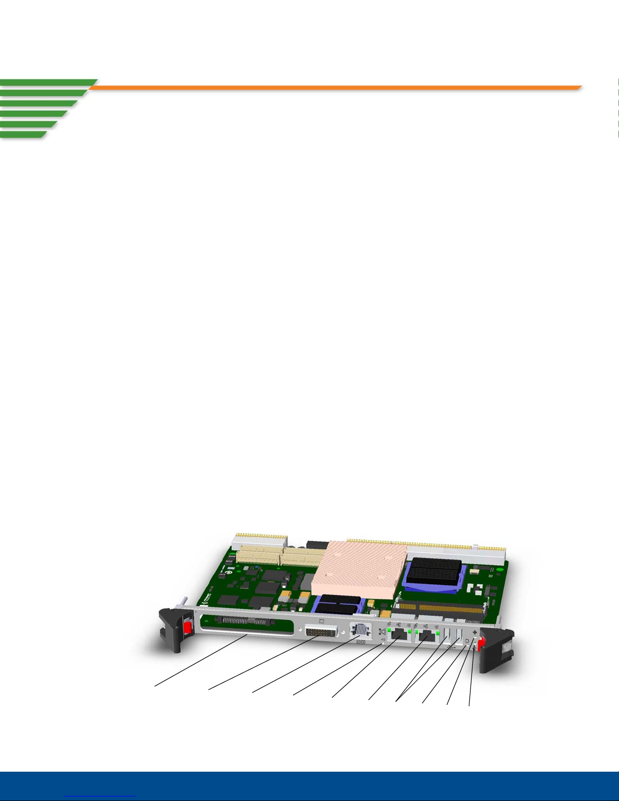
Board Computer. It includes a product definition, a list of product features, a figure showing the
CPC5565 front panel, a functional block diagram, and a description of each block. Unpacking,
initial board configuration, and other setup information are provided in Chapter 3, “Getting
Started.”
Key topics in this chapter include:
• “Product Definition” on page 19
• “CPC5565 Features” on page 20
• “CPC5565 Functional Blocks” on page 22
• “Software” on page 31
Product Definition
Chapter 2
Introduction
The CPC5565 is a CompactPCI® 64-bit, single-slot, single board computer, featuring the Intel
Core 2 Duo dual core 2.2 GHz processor, designed for high-performance embedded
applications. The board incorporates the Intel 3100 integrated northbridge/southbridge chipset,
supporting an 800 MHz front-side bus interface, 400 MHz 64-bit PC2-3200 DDR2 memory
interface. 64-bit PC2-3200 DDR SDRAM up to 8 GB is supported.
The CPC5565 includes support for high-performance video, audio, and storage, featuring the
Advanced Micro Devices (AMD)/ATI Radeon™ E2400 video processor and Serial Advanced
Technology Attachment (SATA) hard disk drive (HDD) interface. It is designed to deliver
exceptional 2D, 3D, and multimedia graphics performance for embedded systems that may
require video/audio, hard disk drive storage, or both.
Figure 2-1: CPC5565 Front Panel
19
Page 20

Chapter 2: Introduction
CPC5565 Features
• Single Slot 6U PICMG 2.16 compute blade
• CompactPCI Hot Swap Specification, PICMG 2.1, R 2.0 compliant
• CompactPCI PTMC Specification, PICMG 2.15 R1 compliant
• CompactPCI Packet Switched Backplane Specification, PICMG 2.16, R 1.0 compliant
• CompactPCI System Management Specification, PICMG 2.9, R 1.0 compliant
• IPMI v1.5 Specification compliant
• 2.2 GHz dual core Intel Core 2 Duo processor (T7500)
• Intel 64 architecture
• Supports Intel Architecture with Dynamic Execution
• PC2-3200 DDR2 400 MHz memory controller interface
• 32 KB Level 1 instruction cache (per core)
• 32 KB Level 1 data cache (per core)
• Up to 4 MB Level 2 shared cache with Advanced Transfer Cache Architecture
• 800 MHz, Source-Synchronous front-side bus
• Intel Virtualization Technology
• Execute Disable Bit support for enhanced security
• System management bus
• Card edge interface contains two SATA channels, eight-lane PCI Express bus, and dual SERDES
1Gb/2.5 Gb Ethernet channels
• Intel 3100 Chipset
• Dual 10/100/1000 Mb/s Ethernet links are available on the front panel via RJ45 connectors
• AMD/ATI Radeon™ E2400 Video Processor
– Internal 128 MB GDDR3 memory
– High-performance 2D, 3D, and multimedia graphics
– QXGA resolution up to 2048 x 1536
– HDMI output for 480p, 720p, and 1080i
– 32 bits per pixel
– DirectX 10 and OpenGL 2.0 support
– Video acceleration
- Advanced de-interlacing algorithms
- Programmable, independent gamma control for video overlay
– SMARTSHADER™ 4.0
– SMOOTHVISION™ 2.0
– Dual-display mode
– Integrated HD audio codec supports PCM and Dolby® Digital 5.1 audio formats
20
Page 21

CPC5565 Features
• Support for 1 PMC slot (2 PMC ports) or one SATA drive (6 SATA ports)
• Supports up to 8 GB of PC2-3200 DDR2 SDRAM with ECC in two 200-pin SO-RDIMM sockets
• PT's Embedded BIOS (AMI core) stored in local flash memory
• Supports Windows® XP, Linux®, and Solaris™ 9/10 64-bit operating systems
• IPMI interface on the backplane
• Standard AT® perip he ra ls inc lud e:
– Real-time clock/CMOS RAM
– 16C550 RS-232 serial port
– USB 2.0 port
• Dual-stage watchdog timer
• Push-button reset switch
• LEDs:
– USER LED, dual color (green/yellow) accessible through an I/O port address
– Hot Swap (Blue/Off)
– Front Panel Ethernet Link (Green)
– Front Panel Ethernet Traffic (Flashing Yellow)
21
Page 22
Chapter 2: Introduction
Rear VGA Video
PCI 33/66 MHz
J5 J3 J2 J1
Intel© 3100
Whitmore
Lake IMCH
Rear SATA Drive (up to 4 SATA Ports)
Rear Serial Port
PTMC Ethernet
2.16 Ports 1 and 2
PCI 33/66 MHz
Intel©
Core
™ 2
Duo
2.2 GHz CPU
Up to 8 GB
400 MHz DDRII
w/ECC 2 SODIMM
SOCKETS
SATA Drive
Connector
Hotswap Switch/
LEDs
RJ45
DVI-I
USB
Conn.
USB
Conn.
RS232
XCVR
IPMC
PAL
BIOS
Flash
Clock
Drivers
PCIE to
PCI
Bridge
Intel
©
82571EB
Broadcom
5389
Broadcom
5466R
PCI to PCI
Bridge
Broadcom
5482S
RJ45
RJ45
JTAG
Binary
FSB
800 MHz
SATA
LPC Bus
SPI
Console
Port
PC3200
PCIE (x4)
USB 2.0
USB 2.0
UART1
IPMB
PCIE (x4)
PCIE (x4)
AMD/ATI
E2400
Video Chip
CPC5565 Functional Blocks
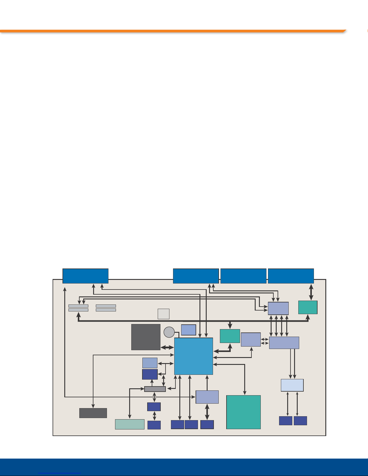
Figure 2-2 is a functional block diagram of the CPC5565. The topics following the figure provide
overviews of the functional blocks:
• “Processor” on page 23
• “Chipset” on page 23
• “CompactPCI Bus Interface” on page 24
• “Intelligent Platform Management Controller” on page 24
• “Memory” on page 25
• “Universal Serial Bus (USB)” on page 25
• “AMD/ATI Radeon E2400 Video Processor” on page 25
• “Serial I/O” on page 27
• “Ethernet Interface” on page 27
• “SATA Interface” on page 28
• “Rear Transition Module (Optional)” on page 28
• “PTMC Interface (Build Option)” on page 28
• “Drone Mode” on page 29
• “Real-Time Clock, CMOS RAM and Battery” on page 29
• “Reset” on page 30
• “Two-Stage Watchdog Timer” on page 30
• “LED Indicators” on page 30
• “Rear-Panel I/O” on page 31
Figure 2-2: CPC5565 Functional Block Diagram
22
Page 23

Processor
The CPC5565 incorporates the Intel Core 2 Duo T7500 processor. The Intel Core 2 Duo T7500
processor is a 2.2 GHz, 35 W (TDP), high performance, low power, 64-bit processor that is
compatible with 32-bit applications, enabling a single architecture across 32- and 64-bit
environments.
The Intel Core 2 Duo implements dual-core technology that puts two mobile-optimized
execution cores in a single processor that is designed to increase performance with significant
power savings. Each core can complete up to four full instructions simultaneously using an
efficient 14-stage pipeline. The two cores share 4 MB of L2 cache, offering more efficient data
sharing, providing enhanced performance, responsiveness and power savings. Each core
utilizes enhanced Intel S peedstep technology on each co re independently t o coordinate powermanagement state transitions and help save power. The 800 MHz front-side bus provides a
high-speed interconnect with the Intel 3100 chipset.
The topic “Processor” on page 117 , contains a link to additional information for this device.
Chipset
CPC5565 Functional Blocks
The CPC5565 incorporates the Intel 3100 integrated chipset. The Intel 3100 chipset integrates
the traditional north/south bridge functions as well as some SuperI/O and peripheral IC features
into a single IC. The Intel 3100 features:
• Processor/Host bus support:
– 64-bit, 800 MHz front-side bus interface
– Up to 36-bit host interface addressing support
– Dynamic bus inversion to minimize power consumption on the data interface
– In-Order Queue (IOQ) depth of 12, with debug support for the one-deep non-pipelined mode
– Two outstanding DEFER cycles supported
– AGTL+ driver technology with parallel termination
• Memory Interface
– Support for two dual rank, registered SO-RDIMMs with ECC
– Support for 15-bit address bus, 72-bit data bus (64-bit data plus 8-bit ECC)
– Support for base DDR2 clock rate of 200 MHz: data interface double-pumped to 400 MT/s, data
bandwidth of 3.2 GB/s
– Support for 512 Mb, 1 Gb, and 2 Gb DRAM densities
– Support for SO-RDDR2 DIMMs using x8 DRAM technology
– Aggressive page-close policy with one-deep, look-ahead to minimize occurrence of page-miss
accesses in favor of page-empty
– Support for standard SEC-DED (72, 64) ECC
– Support for automatic read retry on uncorrectable errors
– Hardware ECC auto-initialization of all populated DRAM de vi ce s un der so ftware control. Includes
pre-selected hardware pattern based memory test on programmable regions.
23
Page 24

Chapter 2: Introduction
• PCI-Express interface features:
– x8 interface capable of bifurcation into two logically independent x4 interfaces with full
specification compliance at half the bandwidth capability
– Low latency, high bandwidth
– 32-bit CRC protection on all packets
– CRC errors are recoverable by retransmission
– Supports 64-bit addressing
– Advance error detection and error transmission on destination bus
– Integrated bit-error generation and monitor function
– PCI-E v1.0 and v1.0a compliant
– Statistics for SNMP MIB II, Ethernet like MIB, and Ethernet MIB (802.3z, Clause 30)
CompactPCI Bus Interface
The CPC5565 does not support a CompactPCI interface at backplane connector J4. The
supported connectors provide access to the following signals:
J1/J2: 3.3V/5V PCI 32 bit 33/66 MHz System Master (driving clocks)
J3: Two PICMIG 2.16-compliant Ethernet ports
J5: Three fixed SATA interfaces (one additional as a load option). JTAG port for test/debug/
manufacturing purposes
See “Backplane Connectors” on page 87 for location and pinout information for these
connectors.
The CPC5565 is compliant with:
• PICMG 2.0 CompactPCI Core Specification
• PICMG 2.1 CompactPCI Hot Swap Specification
• PICMG 2.16 R1 CompactPCI packet-switched backplane (Ethernet) Specification
• PICMG 2.9 R1.0 CompactPCI System Management Specification
“PICMG Specifications” on page 116 contains links to the PICMG Web site, where these
CompactPCI Specifications may be obtained.
The CPC5565 supports hosting hot-swap peripherals in a powered system. The CPC5565 can
also function in a standard (non-hot swap) CompactPCI system.
Intelligent Platform Management Controller
The CPC5565 includes an Intelligent Platform Management Controller (IPMC or BMC) based
on the Atmel ATMEGA128L-8MU, which interfaces to the LPC bus, provides System
Management Bus (SMB) interfaces, and is IPMI compliant. The IPMC subsystem monitors,
controls, and performs remote diagnostics for many on- and off-board functions through IPMI
(Intelligent Platform Management Interface) compliant system management bus interfaces.
24
Page 25

CPC5565 Functional Blocks
The IPMC monitors system sensors for system management events, such as overtemperature,
out-of-range voltages, fan failures, etc., and logs any occurrences in its non-volatile System
Event Log (SEL). You can view the SEL in the BIOS setup utility by selecting the IPMI 1.5
Configuration menu under the Advanced tab on the main menu. The IPMC also provides the
interface to the sensors and SEL so system management software can poll and retrieve the
present status of the system.
Note: The BIOS cannot currently display the IPMC SEL as there is no SEL implemented in the
IPMC firmware at this time. Currently the BIOS maintains its own event log, but does not have
access to any of the management sensors, so will only report BIOS errors. An IPMC SEL will
be implemented in the future and at that time the BIOS will switch from a local event log to
using the IMPC SEL. Currently, there is no IMPI submenu in the Advanced menu.
See Chapter 4, “System Monitoring and Alarms,” on page 57 for more information on IPMC
functionality, supported commands, CPC5565 sensors, and the firmware upgrade process.
The CPC5565 is compliant with standard Intelligent Platform Management Interface v1.5
Specification functionality. See “Intelligent Platform Management Controller” on page 116, for
information about this specification.
Memory
The CPC5565 includes two 200-pin, Small Outline Registered Dual In-line Memory Module
(SO-RDIMM) socket that can be populated with up to 8 GB DDR2-400 registered SDRAM. The
BIOS automatically determines the SDRAM's size and speed.
Universal Serial Bus (USB)
The Universal Serial Bus (USB) provides a common interface to many peripherals such as
keyboard, serial ports, and mouse ports. The CPC5565 supports booting from USB devices,
such as CD-ROM, DVD, or thumb drive.
The CPC5565 supports two standard USB 2.0 ports, available at the front panel. See Figure
2-1, “CPC5565 Front Panel,” on page 19. A third USB port is directed to the backplane via
RPIO connector J5. See “J5 (Rear-Panel User I/O Connector)” on page 90.
The CPC5565's USB resides in the Intel 3100 chipset. The topic “Chipset” on page 115
provides a link to the data sheet for this device. Connector locations and pinouts are
documented in the topic “USB Connectors (J10, J15)” on page 93.
AMD/ATI Radeon E2400 Video Processor
The CPC5565 incorporates the high performance AMD/ATI Radeon E2400 video processor,
which delivers exceptional 2D, 3D, and multimedia graphics performance for embedded
systems. It has 128 MB of internal GDDR3 Synchronous Graphics RAM (SGRAM) memory
(two pieces of 16Mx32) integrated in the application-specific integrated circuit (ASIC) package.
The AMD/ATI Radeon E2400 video processor supports DirectX 10 with Shader Model 4.0,
integrated Transition Minimized Differential Signaling (TMDS), and a Universal Video Decoder
(UVD), which supports HD-DVD and Blu-ray Disc™ decode (H.264 or VC-1 formats).
25
Page 26

Chapter 2: Introduction
The AMD/ATI Radeon E2400 video processor represents ATI's third-generation PCI Express
technology product and leverages a new graphics architecture. Based on 65 nm process
technology, the AMD/ATI Radeon E2400 video processor delivers a 16-lane PCI Express bus
interface and RoHS compliant ASIC.
Video Features
The AMD/ATI Radeon E2400 video processor provides one of the fastest and most advanced
2D, 3D, and multimedia graphics performances based on PCI Express bus architecture. The
E2400 supports PCI Express, DirectX 10 features, highly optimized Open Graphics Library®
2.0 support, and flexible memory configurations.
The AMD/ATI Radeon E2400 video processor supports the following video features:
SMARTSHADER 4.0 - Advanced Shader Technology
• Provides complete hardware-accelerated support for the DirectX 10 programmable shader model,
enabling more complex and realistic texture and lighting effects
• Significant improvement over first-generation shaders introduced in DirectX 8, with a more powerful
and intuitive instruction set
• Offers full support for this feature in OpenGL 2.0 applications
SMOOTHVISION 2.0 - Flexible Anti-Aliasing and Anisotropic Filtering
• 2x/4x/8x full-scene anti-aliasing modes
• Adaptive algorithm with programmable sample patterns
• 2x/4x/8x/16x anisotropic filtering modes
• Adaptive algorithm with bi-linear (performance) and tri-linear (quality) options
• Temporal anti-aliasing
Avivo™ Display Support - Two Fully Functional Displays
• Traditional Cathode Ray Tube (CRT) monitors and DVI-D are supported
• Features dual channel DVI-D support
• 230 MHz Low-Volt age Differential Signalin g (LVDS) transmitter supports Liquid Crystal Display (LCD)
panels up to Quad eXtended Graphics Array (QXGA) (2048x1536) resolution
• Integrated TMDS transmitter that supports:
– 1600x1200 resolution without reduced blank timings when matched with coherently clocked
receivers
– 1920x1440 resolution with reduced blank timings when matched with coherently clocked
receivers
– 1600x1200 resolution with reduced blank timings when matched with incoherently clocked
receivers
• Supports standard single channel DVI-D, or Digital Flat Panel connections. Includes integrated
conversion of 30 bpp data to either 24 bpp or 18 bpp, depending on attached panel type.
• High performance DAC speeds of 400 MHz
26
Page 27

Video Acceleration
• The E2400 video processor allows integration of digital video features including advanced
• Features in Detail and Motion Compensation (MC) support for the acceleration o f MPEG encoding
See “AMD/ATI Radeon E2400 Video Processor” on page 115 for a link to additional information
for this device.
Serial I/O
The CPC5565 provides one 16C550, PC-compatible serial port. COM1 is available at the front
panel via 8-pin RJ-45 connector J7 and is also available to an RTM via RPIO connector J5.
J7 is also routed to the IPMC console port for remote IPMC configuration. The console port
mux is designed to be controlled from either the IPMC or the payload and to automatically
default to the IPMC when the payload is powered down or powered up with unconfigured
programmable devices.
CPC5565 Functional Blocks
deinterlacing algorithms for high-quality video and integrated digital TV decode capability. Includes
programmable, independent gamma control for the video overlay.
and decoding as well as Digital Video (DV) encoding and decoding.
J7 is compatible with RS-232 signaling levels and 15KV ESD protection are provided by the
interface. The port supports data transfers a t speeds up to 115.2 Kb/sec. The baud rate is set if
either console redirection or serial checkpoints is enabled. When the BIOS sets the baud rate
for either of those features, the default is 9600 bps. If neither feature is enabled, the COM port
is not configured by the BIOS. See the topic “BIOS Configuration Overview” on page 40 for
more information about BIOS setup.
The front panel RJ-45 serial port support s flow control. The rear panel serial port connection at
J5 has the signalling reduced to simply Rx and Tx, and does not support flow control signalling.
The CPC5565's serial controller resides in the Intel 3100 chipset. The topics “I/O Controller” on
page 116 and “Intelligent Platform Management Controller” on page 116 provide links to more
information for these devices. Connector locations and pinouts are documented in Chapter 5,
“Connectors.”
See “BIOS Configuration Overview” on page 40 for more information about BIOS setup. For
Console port pinout information, see “RS-232 RJ-45 Console Port (J7)” on page 92.
Ethernet Interface
The CPC5565 provides eight on-board 10/100/1000Base-T Ethernet channels through the onboard Broadcom BCM5389 8GbE Port Switch. Ethernet channels can be directed through the
BIOS setup utility , providing basic connectivity and functionality on power up and reset. See the
topic “BIOS Configuration Overview” on page 40 for more information.
The eight on-board Ethernet channels are as follows:
• Front panel RJ-45 connectors J8 and J9 (Front Panel A and Front Panel B BIOS setup options).
These connectors each have two LEDs to indicate the status of that channel.
• Two channels to midplane connector J3 (2.16 A and 2.16 B BIOS setup options)
• Two channels to optional on-board PMC site J11-J14 (PMC A and PMC B BIOS setup options). This
site provides an interface for a dual channel gigabit Ethernet PMC mezzanine card. The site
conforms to Option 7 of the PTMC Specification. The PMC card must have transformers on it to
27
Page 28

Chapter 2: Introduction
provide isolation from the CPC5565. See the topic “PTMC Interface (Build Option)” on page 28 for
more information about the site.
• Two channels to the host CPU via the 82571 dual NIC (ENET A and ENET B BIOS setup options).
The on-board devices are grouped in pairs to support link aggregation to the switch to allow
greater throughput and redundancy during normal operation.
The topic “Ethernet” on page 115, contains links to the product brief for the Broadcom
BCM5389 Ethernet controllers used on board the CPC5565. Connector locations and pinouts
are documented in Chapter 5, “Connectors,” on page 79.
SATA Interface
The CPC5565 includes an integrated Serial ATA (SATA) controller that routes five independen t
SATA interfaces, each of which is SATA 1.0 compliant:
• SATA drive mounted to the on-board SATA connector (build option)
• Four SATA ports routed to RPIO connector J5
The CPC5565's SATA controller resides in the Intel 3100 chipset. The topic “Chipset” on
page 115 provides a link to the data sheet for this device. RPIO connector J5 location and
pinout are documented in the topic “J5 (Rear-Panel User I/O Connector)” on page 90.
Rear Transition Module (Optional)
The RTM4811, an advanced rear transition module, offers support for a SA TA 2.5-in. hard drive
disk, an analog VGA video interface, and USB. The CPC5565 can boot from SATA storage on
this RTM or through a SATA connector on the RTM faceplate.
By using the RTM4811, the CPC5565 can be chained to a CPC5910 storage expansion
module that contains two SATA 3.5-in. hard drive disks to make a local storage array with up to
3 TB of directly attached storage. See the topic “User Documentation” on page 117 for links to
more information about the RTM4811 and CPC5910.
PTMC Interface (Build Option)
The CPC5565 is optionally also a PMC carrier card that supports the following specifications:
• Complies with PICMG 2.15 R1.0 configuration 7 (PT7CC)
• Dual channel Ethernet links (MDI) compatible with PICMG 2.15 ECN 2.15-1.0-001 (Ethernet MDI
Links on PTMC, configurations 5 and 6)
• Complies with IEEE1386.1 PCI Mezzanine Card (PMC)
• Complies with VITA 39: PCI-X for PMC (133 MHz)
• Complies with PCI-E v1.0 and 1.0a (PCI-Express)
• Support 3.3V VIO Cards Only
The PCI Telecom Mezzanine Card (PTMC) interface is compatible with the PICMG 2.15
PT7CC Specification. The PTMC provides a way to add modules such as IPSec accelerators
and network processors to increase baseboard functionality.
28
Page 29

CPC5565 Functional Blocks
The CPC5565 PTMC site provides an industry-standard interface for a high performance, dual
channel, gigabit Ethernet PMC mezzanine card. High performance is achieved by means of a
64-bit wide, 66 MHz interface that is capable of PCI or PCI-X signaling. Dual channel Ethernet
links (MDI) are routed on PTMC interface connectors J1 1-J14 per PICMG 2.15 configurations 5
and 6. The Ethernet links can be routed to CPC5565 rear-panel gigabit Ethernet connector J3
for connection to the CompactPCI backplane per PICMG 2.16.
Note: PCI-X is supported only when operating in Drone Mode.
The CPC5565 is backward compatible with all standard 32-bit and 64-bit PMC cards. However,
these cards do not respect the PTENB# signal. We advise caution when installing a standard
PMC card with P4 (rear I/O) signaling. Please check the pinout carefully: Connector J1 4 on the
CPC5565 has pins 1 - 24 set to support two 1 Gigabit Ethernet channels. Make sure this
definition does not interfere with the operation of the PMC card installed.
PMC modules interfacing to the CPC5565 must advertise their PTID (PCI Telecom Identifier)
as “configuration 7” before they are enabled (PTENB# asserted). PMC modules supporting
configurations 1, 2, 3, 4, 5, 6 will not have their PMC interface enabled by PTENB#.
The mezzanine interface is at J11-J14 on the CPC5565. See Chapter 5, “Connectors,” on
page 79 for more information.
Drone Mode
The CPC5565 can be set to operate in Drone mode when installed in a non-system slot in a
CompactPCI chassis. In Drone mode it cannot drive the system clock or the CompactPCI bus.
The CPC5565 can optionally be reset by the System Master when in a peripheral slot. See the
topic “SW3-3 Force Drone Mode” on page 39 for more information.
Real-Time Clock, CMOS RAM and Battery
The real-time clock performs timekeeping functions and includes 256 bytes of battery-backed
CMOS RAM in two banks that are reserved for BIOS use. Timekeeping features include a timeof-day clock and a multi-century calendar with alarm features and century rollover. The time,
date, and CMOS values can be specified or returned to their defaults by using the BIOS setup
program. See the topic “BIOS Configuration Overview” on page 40, for more information.
Note: The recommended method of accessing the date in systems with PT Single Board
Computers is indirectly from the real time clock via the BIOS. The BIOS on PT Single Board
Computers contains a century checking and maintenance feature. This feature checks the two
least significant digits of the year stored in the real time clock during each BIOS request (INT
1Ah) to read the date and, if less than 80 (1980 is the first year supported by the PC), updates
the century byte to 20. This feature enables operating systems and applications using the BIOS
date/time services to reliably manipulate the year as a four-digit value.
Two rechargeable button-cell batteries located on the CPC5565 power the real-time clock and
CMOS memory when the CPC5565 is not powered externally. The battery is intended for AC
power fails only and has an estimated life of 60 days (with batteries fully charg ed). It recharges
whenever standby power is present.
The CPC5565's real-time clock resides in the Intel 3100 chipset. The topic “I/O Controller” on
page 116, provides a link to more information for this device.
29
Page 30

Chapter 2: Introduction
Reset
The CPC5565 provides the following reset types:
• Push-button reset
• IPMC generated reset (Payload Reset)
• Watchdog timer reset
See Chapter 6, “Reset” for more information.
Two-Stage Watchdog Timer
The watchdog timer optionally monitors system operation and is programmable for one of
many different timeout periods (from 1µs to 1050s). It is a two-stage watchdog, meaning that it
can be enabled to produce a SERIRQ, NMI or SMI interrupt during the first stage followed by a
system reset for the second stage. Failure to strobe the watchdog timer within the programmed
time period may result in an NMI/SMI/SERIRQ, a system reset, or both. A register bit is set if
the watchdog timer caused the reset event.
The CPC5565's two-stage watchdog timer resides in the Intel 3100 chipset. The topic “Chipset”
on page 115, provides a link to the datasheet for this device.
LED Indicators
The LEDs located on the front panel are defined below. See Figure 2-1, “CPC5565 Front
Panel,” on page 19 for LED locations.
User LED
Bicolor LED controlled by system register settings See the topic “Programming the LEDS” on
page 59, for more information.
• Green = user defined
• Yellow = user defined
• Off = user defined
Front Panel Ethernet (RJ-45 Connector)
Each Ethernet connector on the front panel includes two LEDs:
• Ethernet Speed (Top)
– Green = 100 Mb/s
– Orange = 1000 Mb/s
– Off = 10 Mb/s
• Ethernet Link (bottom)
– Yellow = Link
–Off = No Link
30
Page 31

Hot Swap
• Blue = safe to extract board
• Off = not safe to extract board
• Short Blink = payload is shutting down
Status/Health
• Off = payload not powered
• Green = healthy (amber conditions not met)
• Amber = at least one threshold sensor has crossed a critical threshold, the payload is held in reset,
power is not good (as detected by HW), the processor is reporting CPU Error, the processor is
reporting Therm Trip, or the processor is in ACPI sleep state 5.
Rear-Panel I/O
The CPC5565 transitions the following I/O signals through CompactPCI connector J5 to an
optional Rear Transition Module:
Software
• COM port
•Video
• Power and Ground
•USB
•SATA
•SMBus
• RPIO Present
•Eject
•JTAG
In addition, the CPC5565 transitions Gigabit Ethernet A and B through CompactPCI connector
J3.
See Chapter 5, “Connectors,” on page 79 for more information on the connectors present on
the CPC5565.
Software
BIOS
The PT Embedded BIOS (AMI core) is user-configurable to boot an operating system from one
of the following locations:
• USB mass storage device (hard drive, DVD-ROM or CD-RO M dr ive , flash driv e, etc. )
• Serial ATA (SATA) hard drives
•Ethernet (PXE)
• Any add-on cards/boards that support a BIOS boot specification option ROM
31
Page 32

Chapter 2: Introduction
Operating Systems Supported
Both 32- and 64-bit operating systems are supported:
• WinXP and WinXP 64 have been installed and successfully run through Microsoft's Hardware
Compatibility Test (pending).
• Solaris 10 has been installed successfully (pending). Upon successful completion of Sun Hardware
Compatibility Test Suite (HCTS), results will be posted to Sun's Web page http://www.sun.com/
bigadmin/hcl/overview.html.
• Red Hat Enterprise Linux AS 4 Update 3 (32 and 64 bit versions) has been installed successfully
(pending).
• Nexusware Core has been installed and successfully run th rough PT's validation test suite (pending) .
IPMI
For more information about how to program software to interact with the IPMI firmware, refer to
the Intelligent Platform Management Interface v1.5 Specification and the Intelligent Platform
Management Interface Implementer's Guide. A link to these publications is available in the
topic “Intelligent Platform Management Controller” on page 116.
32
Page 33

Chapter 3
Getting Started
This chapter summarizes the information you need to make the CPC5565 operational. Please
read it before attempting to use the board.
Key topics in this chapter include:
• “Unpacking” on page 34
• “Electrical and Environmental Requirements” on page 34
• “Memory Configuration” on page 34
• “I/O Configuration” on page 36
• “Connectivity” on page 37
• “Switches” on page 37
• “BIOS Configuration Overview” on page 40
• “Installing a PMC Device” on page 54
• “Installing the Operating System” on page 57
• “Programming the LEDS” on page 59
• “Installing the Display Drivers” on page 59
33
Page 34

Chapter 3: Getting Started
Warning:
Warning:
Unpacking
Check the shipping carton for damage. If the shipping carton and co ntents are damaged, notify
the carrier and PT for an insurance settlement. Retain the shipping carton and packing ma terial
for inspection by the carrier. Obtain authorization before returning any product to PT. Refer to
“Customer Support and Services” on page 16, for assistance information.
Like all equipment that uses MOS devices, the CPC5565 must be protected from static
discharge. Never remove any of the socketed parts except at a static-free workstation. Use
the anti-static bag shipped with your order when handling the board.
Electrical and Environmental Requirements
Electrical specifications are presented in detail in “Electrical and Environmental Specifications”
on page 103.
The CPC5565 is supplied with a heat sink that allows the processor to operate between 0° and
approximately 55°C ambient with a minimum of 200 LFM (1.27 meters per second) of external
airflow (verification pending). It is the user's responsibility to ensure that the CPC5565 is
installed in a chassis capable of supplying adequate airflow . The maximum power dissipation of
the processor is 35 W. External airflow must be provided at all times. See Chapter 7,
“Specifications” and Chapter 8, “Thermal Considerations” for more details.
Operating the CPC5565 without adequate airflow will damage the processor.
The CPC5565 may contain materials that require regulation upon disposal. Please dispose of
this product in accordance with local rules and regulations. For disposal or recycling
information, please contact your local authorities or the Electronic Industries Alliance at http://
www.eiae.org/.
Memory Configuration
The CPC5565 can address up to 24 GB of memory that is allocated between system memory
and PCI devices. Two SDRAM sockets provide up to 8 GB of DDR system memory. The
memory address space is divided between memory local to the board (system memory) and
memory located on the two PCI buses. Any memory not reserved or occupied by a local
memory device (DDR or flash) is available to the on-board PMC site.
The CPC5565 is populated with PC2-3200 ECC DDR2 SDRAM located on two registered, 200pin SO-RDIMM sockets. The socket supports up to 8 GB, 200 MHz DDR2-400 (PC2-3200)
memory modules with ECC.
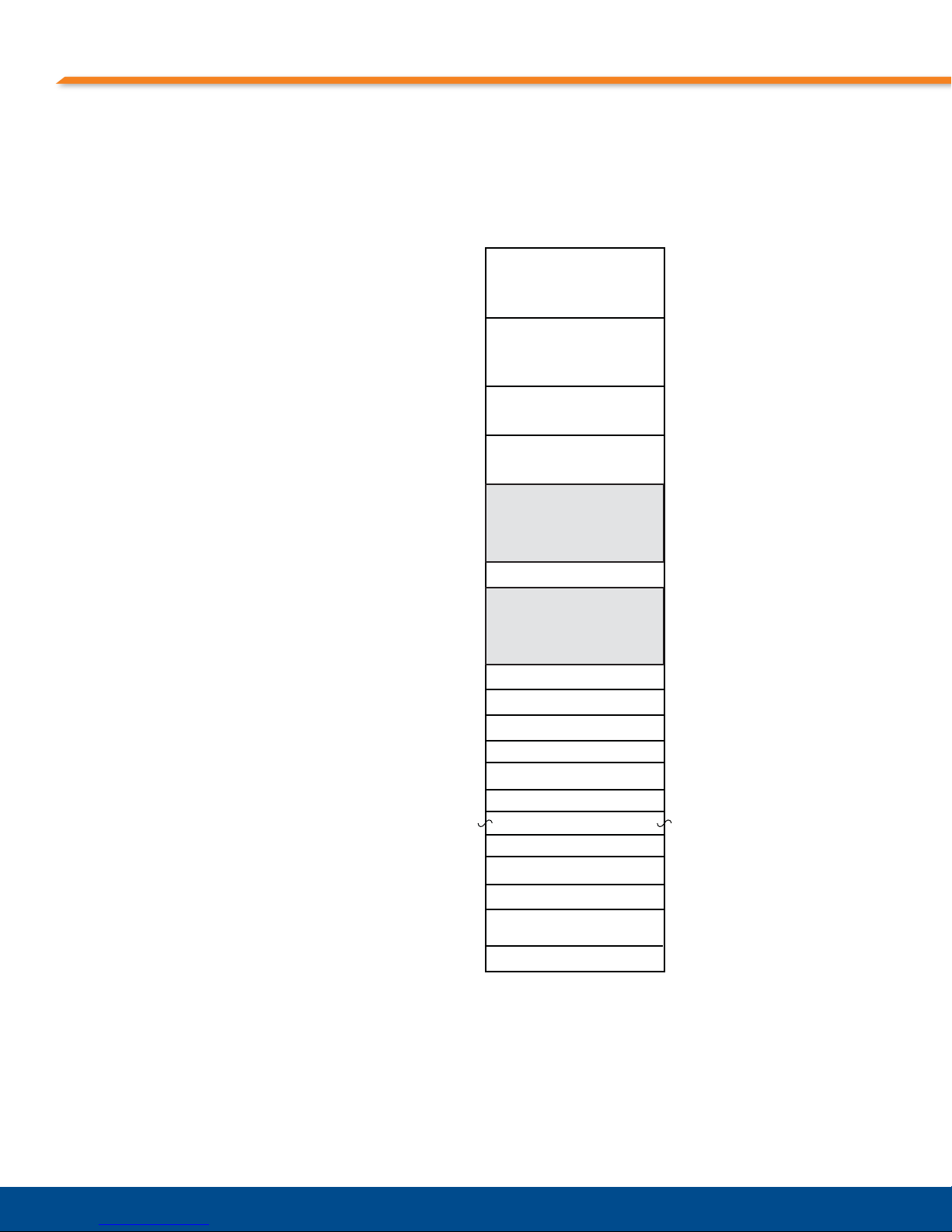
Figure 3-1, “Memory Address Map Example,” on page 35, shows an example of memory
addressing for the CPC5565.
34
Page 35
Memory Configuration
High PCI Memory Range
System BIOS
FEC03000 - FEDFFFFFh
FEE00000 - FEE003FFh
FEC81000 - FEC81FFFh
FEC80000 - FEC80FFFh
FEC00000 - FEC7FFFFh
F0000000 - FEBFFFFFh
Local APIC
I/O APIC 0
I/O APIC 2
I/O APIC 3
FEE00400 - FFEFFFFFh
Reserved (Optional DRAM region)
E0000000 - EFFFFFFFh PCIe Enhanced Config. Aperture
Top of Memory* - DFFFFFFFh PCI
System Memory
System BIOS
VGA BIOS
VGA Display Memory
System Memory
BIOS Extensions/UMB Services
00100000h -Top of Memory*
E0000h - FFFFFh
C8000h - DFFFFh
C0000h - C7FFFh
A0000h - BFFFFh
0h - 9FFFh
Reserved (PCI)
Reserved (PCI)
FFF00000 - FFF7FFFFh
FFF80000 - FFFFFFFFh
System Memory
100000000 - Top of Memory 2
Top of Memory 2 - 64 GB
ESCD/NVRAM
Memory is not a field serviceable item. Return the module to PT for memory replacement. See
“Return Merchandise Authorization (RMA),” on page 17, for more information about returning
merchandise.
Figure 3-1: Memory Address Map Example
Note: *This address varies depending on how much RAM is installed and how much address
space is required by PCI devices. The default PCI address base is 3 GB. If the amount of
installed RAM is less than the PCI address base this will be the top of physical memory. If more
RAM is installed this is the PCI address space base address and system memory continues
above 16 GB up to the top of memory.
35
Page 36

Chapter 3: Getting Started
I/O Configuration
The CPC5565 addresses up to 64 KB of I/O using a 16-bit I/O address.
The CPC5565 is populated with many of the most commonly used I/O peripheral devices for
industrial control and computing applications. The I/O address location for each of the
peripherals is shown in Figure 3-2.
Figure 3-2: I/O Address Map
CFCh PCI Configuration Data Register (double word)
CF9h
CF8h
600 - 618h
500h
540h
4D0 - 4D1h
460h
400h
3F6h
376h
1F0 -1F7h
170 -177h
E1-E8h
C0 – DFh
B4 - BDh
B2 - B3h
A0 - B1h
93 – 9Fh
92h
81 - 91h
78 - 80h
70 - 77h
64h
60h
50 - 53h
4Fh
4Eh
40 - 43h
31 - 3Dh
20 - 2Dh
0 - 1Fh
PCI Configuration Index Register (double word)
Chipset Power Management Base
On-board Slave Interrupt Controller
On-board Master Interrupt Controller
Reset Generator
Watchdog Timer
Chipset GPIO Base
Chipset SMB Base
Interrupt Controller
Chipset TCO Base
SATA
SATA
SATA
SATA
CPC5565 System Registers
On-board Slave DMA Controller
Interrupt Controller
Power Management
DMA Controller
Fast Gate A20/Reset Control
On-board DMA Page Registers
CPC5565 System Registers
NMI Enable/RTC Controller
Keyboard/Mouse
Keyboard/Mouse
Timer/Counter
IO Data (Write Only)
IO Index (Write Only)
On-board Timer/Counters
Interrupt Controller
On-board Master DMA Controller
36
Page 37
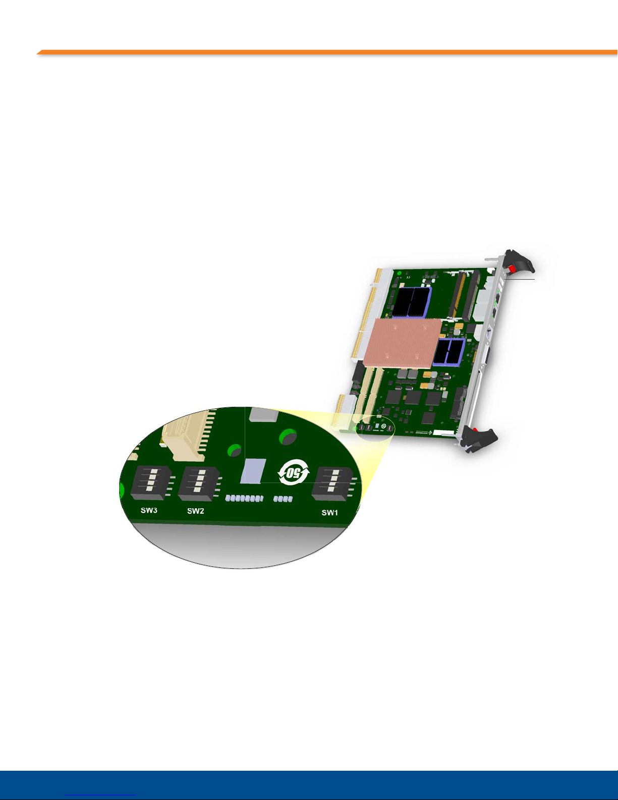
Connectivity
PushButton
Reset
(SW4)
The CPC5565 provides several connectors for interfacing to application specific devices. Refer
to Chapter 5, “Connectors,” for complete connector descriptions and pinouts.
Switches
The CPC5565 includes three switch packs and a front panel reset switch as shown in
Figure 3-3, “Switch Locations.”
Figure 3-3: Switch Locations
Connectivity
Switch Pack 1 (SW1)
SW1 is a four-position, single-pole DIP switch pack. See Figure 3-3, “Switch Locations,” for the
switch position on the CPC5565. SW1 controls the following functions.
SW1-1: PCIXCAP Override on Local PCI Bus
Open = Determined by PMC
Closed = PCIXCAP is forced low (PCIX disabled)
37
Page 38

Chapter 3: Getting Started
SW1-2: COM Port Override
Open = Console port is owned by the payload when the payload is powered and out of reset
(default)
Closed = Console port is owned by the IPMC at all times (note that in this mode SW3-1 switch
status is irrelevant as the payload won't have the console port to display post codes)
SW1-3: IPMC JTAG Selection
Reserved; Do not change this switch setting
SW1-4: Drone Reset Control
Open = Board can be reset based on PCI reset (J1) when installed in the system master slot
(default)
Closed = Board can be reset based on PCI reset (J1) if it is operating in a non-system master
slot (drone mode)
Switch Pack 2 (SW2)
SW2 is a four-position, single-pole DIP switch pack. See Figure 3-3, “Switch Locations,” for the
switch position on the CPC5565. SW2 controls the following functions.
SW2-1: Clear CMOS
During normal operation this switch is open. Close SW2-1 to clear CMOS.
SW2-2, SW2-3: User Switch Bits
These switches set user switch bits as follows:
SW2-2: user switch bit 0
SW2-3: user switch bit 1
SW2-4: Console Redirection
During normal operation this switch is closed, enabling console redirection. To disable console
redirection, open SW2-4 and disable the CMOS option in the BIOS setup. See “BIOS
Configuration Overview,” on page 40, for more information.
38
Page 39

Switch Pack 3 (SW3)
SW3-1 Port 80 Post Codes Out Serial Port (Front Panel)
Open = Disabled (default)
Closed = Enabled
SW3-2 Reserved
Reserved; Do not change this switch setting.
SW3-3 Force Drone Mode
Open = Uses SYSEN# to determine system master/drone mode (default)
Closed = Forces drone mode operation
Switches
SW3-4 Reserved
Reserved; Do not change this switch setting.
Push-Button Reset (SW4)
SW4 is a push button on the CPC5565's front panel. Pressing SW4 forces a hard CPU reset
and holds the board in reset until SW4 is released. See Figure 2-1, “CPC5565 Front Panel,” on
page 19 for the switch location.
Hot-Swap Switch (SW5)
SW5 is the hot-swap ejector switch on the lower ejector handle. Its function and behavior is
defined by PICMG 2.1. The ejector handles are used when the CPC5565 is inserted or
removed (hot swapped) from a chassis that is powered on. Before removing a board from a
system that is powered on, open the ejector handles just enough to disengage them from the
chassis, but without fully disengaging the bus connectors from the midplane. This causes
software to be notified that the board is about to be removed. Once the blue hot-swap LED on
the front panel is lit, it is safe to completely remove the board from the chassis. See Figure 2-1,
“CPC5565 Front Panel,” on page 19 for the LED location.
The hot swap ejector switch can also be used to signal the IPMC to shut down power to the
payload. To do this, open-close-open the handle within two seconds. This functionality is also
available via the hot swap ejector switch on an optional RTM, such as the PT R TM4811, mated
to the CPC5565. See “Payload Shutdown Timeout,” on page 75, for information about using
the ejector handle to perform a graceful (ACPI) shutdown.
39
Page 40
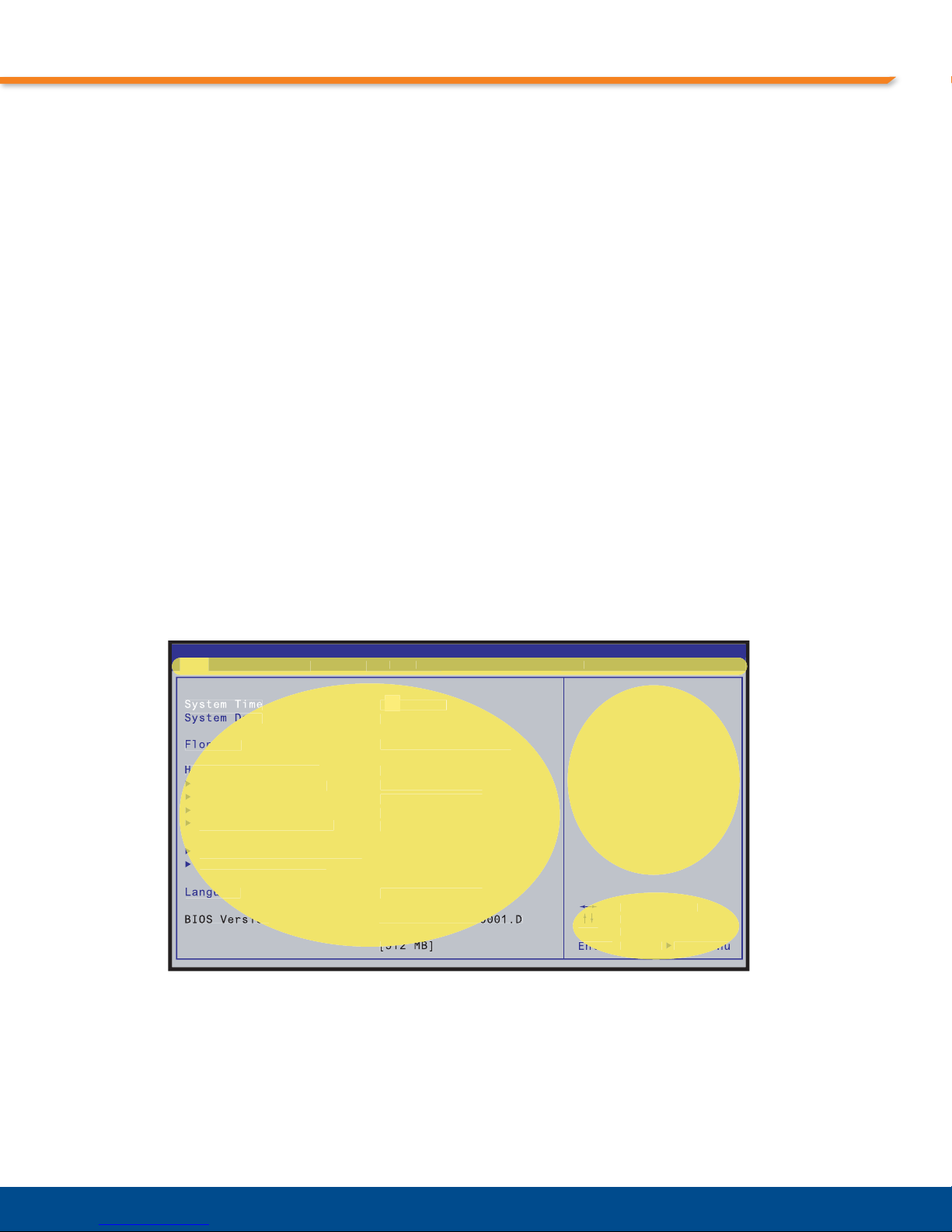
Chapter 3: Getting Started
BIOS SETUP UTILITY
Total Memory
Date
Pri
IDE M
S
S
23
]
]
d]
]
]
KT030LEA.86B.00
Selec
d
Selec
Tab
Sub-Menu
S
S
t
Legend of Keys
Main Setup Screen
MainAdvanced
y
oot
yg
t
Setup Menu
Context
Sensitive Help
BIOS Configuration Overview
The PT Embedded BIOS has many separately configurable features. These features are
selected by running the built-in setup utility. The system configuration settings are saved in a
portion of the battery-backed RAM (CMOS) in the real-time clock device and are used by the
BIOS to initialize the system at boot-up or reset. The configuration is protected by a checksum
word for system integrity.
To access the setup utility, press the F2 key during the POST test and initia lization at boot time.
Setup runs once the POST functions complete.
When Setup runs, an interactive configuration screen displays. See Figure 3-4, “Setup Screen
Layout” , for an example. Setup parameters are divided into d ifferent categories. The available
categories are listed in a menu across the top of the setup screen. The parameters within the
highlighted (current) category are listed in the main (left) portion of the setup screen. Contextsensitive help is displayed in the right portion of the screen for each parameter. A legend of
keys is listed at the bottom of the setup screen.
Use the left and right arrow keys to select a category from the menu. Use the up and down
arrow keys to select a parameter in the main portion of the screen. Use the + or - keys or press
the Enter key to open a list of selections to change the value of a parameter.
Items in the main portion of the screen that have a triangular mark to their left are submenus.
To display a submenu, use the up and down arrow keys to highlight the submenu and then
press the Enter key.
Figure 3-4: Setup Screen Layout
SecurityB
mary
Primary IDE Slave
econdary IDE Master
econdary IDE Slave
Processor Configuration
Ethernet Locations
aster
Sun 12/31/1989]
.44/1.25 MB 3.5"
Disabled
ot Installe
Not Installed
T34311A
CD -540E ]
English (US)]
System Management Exi
elect Menu
t Item
t Fiel
elec
40
Page 41

Ethernet Interface
The CPC5565 provides eight 10/100/1000Base-T Ethernet channels through the onboard
Broadcom BCM5389 8GbE Port Switch. Ethernet channels can be configured through the
BIOS setup utility , providing basic connectivity and functionality on power up and reset. See the
topic “BIOS Configuration Overview” on page 40 for more information about the BIOS setup
utility.
The eight on-board Ethernet channels are as follows:
• Front panel RJ-45 connectors J8 and J9 (Front Panel A and Front Panel B BIOS setup options).
These connectors each have two LEDs to indicate the status of that channel.
• Two channels to midplane connector J3 (2.16 A and 2.16 B BIOS setup options)
• Two channels to optional on-board PMC site J11-J14 (PMC A and PMC B BIOS setup options). This
site provides an interface for a dual channel gigabit Ethernet PMC mezzanine card. The site
conforms to Option 7 of the PTMC Specification. The PMC card must have transformers on it to
provide isolation from the CPC5565. See the topic “PTMC Interface (Build Option)” on page 28 for
more information about the site.
• Two channels to the host CPU via the 82571 dual NIC (ENET A and ENET B BIOS setup options).
BIOS Configuration Overview
The topic “Ethernet,” on page 115, contains links to the product brief for the Broadcom
BCM5389 Ethernet controllers used on board the CPC5565. Connector locations and pinouts
are documented in Chapter 5, “Connectors,” on page 85.
41
Page 42
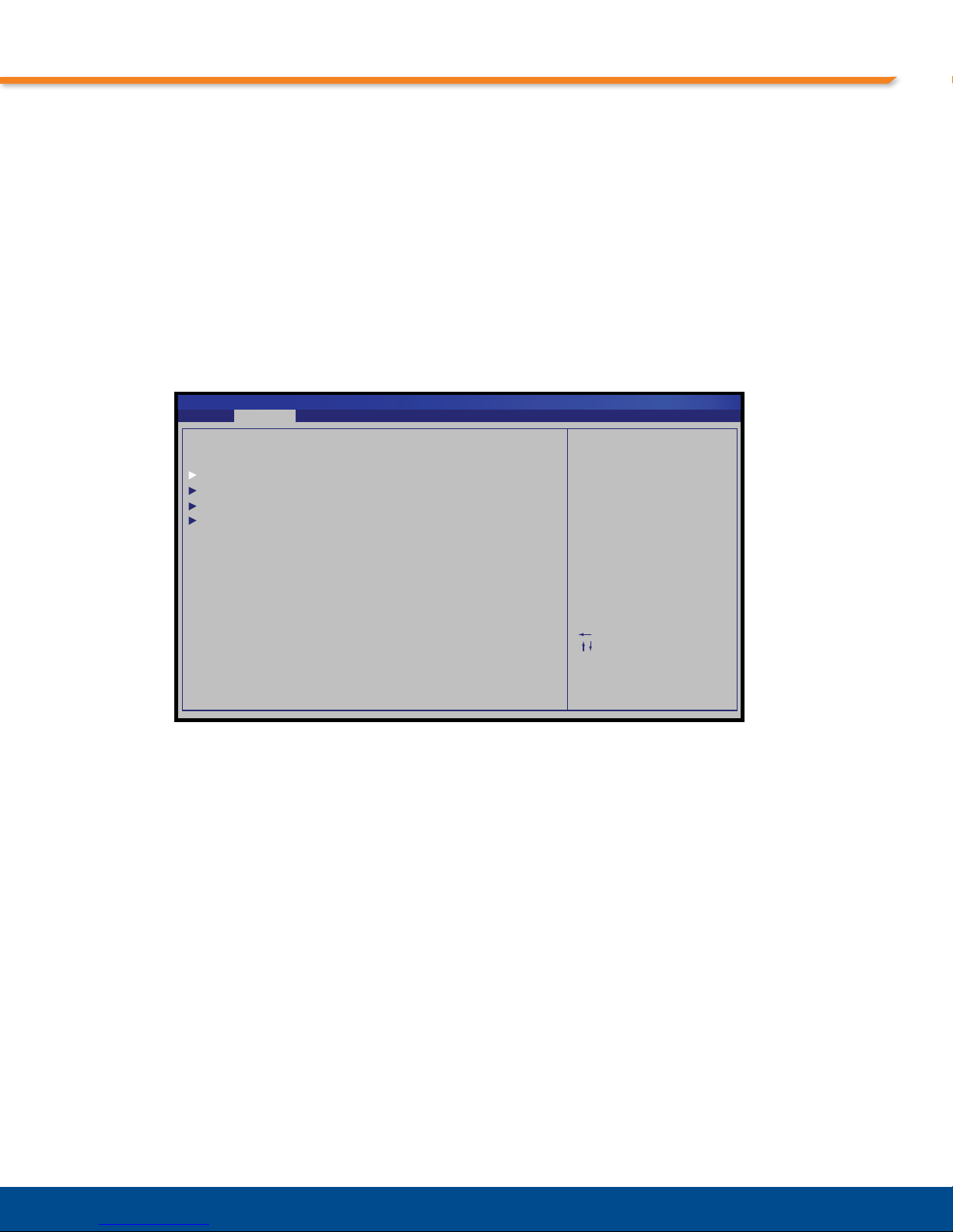
Chapter 3: Getting Started
BIOS SETUP UTILITY
Switch Configuration
ESC
Save and Exit
Select Item
F10
General HelpF1
Select the VLAN
routing for the
switch ports
Enter
VLAN Configuration
Jumbo Frames Configuration
Port Trunking Configuration
MAC Address Handling Configuration
Select Screen
Go to Sub Screen
Exit
Advanced
Ethernet Switch BIOS Options
For CPC5565 BIOS version P05 or later, selecting the Switch Configuration option on the
Advanced tab in the BIOS setup utility brings up the Switch Configuration submenu screen
shown in Figure 3-5, “Switch Configuration Screen.” This screen provides access to the
following options described in the topics below:
• VLAN Configuration
• Jumbo Frames Configuration
• Port Trunking Configuration
• MAC Address Handling Configuration
Figure 3-5: Switch Configuration Screen
VLAN Configuration
A virtual LAN(VLAN) can be configured in the BIOS setup utility. Selecting the VLAN
Configuration option on the Switch Configuration submenu brings up the screen shown in
Figure 3-6, “VLAN Configuration Screen,” on page 43, where the options can be selected.
More advanced control can be achieved with a user-created switch management interface
program for the operating system being used.
VLAN Configurations
Two VLAN modes are available for the BCM5389 Ethernet Switch:
• 802.1Q VLAN Mode
• Port VLAN Mode
42
Page 43
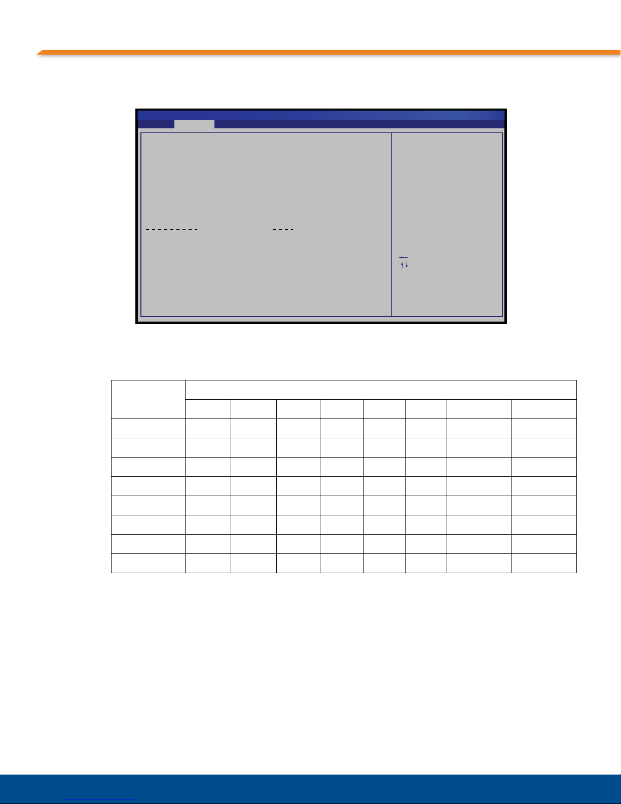
Figure 3-6: VLAN Configuration Screen
BIOS SETUP UTILITY
VLAN Configuration
802.1Q [Enabled]
VLAN Routing
ESC
Save and Exit
Select Item
F10
General HelpF1
Enable 802.1Q
& untag frames to
all egress ports.
Enter
ENET A
ENET B
PMC A
PMC B
2.16 A
2.16 B
Front Panel A
Front Panel B
[1]
[2]
[1]
[2]
[1]
[2]
[1]
[2]
Select Screen
Change Option
Exit
Advanced
Options
No
VLANPort
BIOS Configuration Overview
Table 3-1 indicates the default routing.
Table 3-1: Default Ethernet Routing
Route From:
ENETA XXX
ENETB XX X
PMC A XXX
PMC B XXX
2.16 A XX X
2.16 B XX X
Front Panel A XXX
Front Panel B XXX
802.1Q VLAN Mode
The default VLAN mode is 802.1Q. This mode configures two VLANs with four port s in VLAN 1
and four ports in VLAN 2. When this mode is selected, the default membership is as follows:
VLAN 1:
Route To:
ENETA ENETB PMC A PMC B 2.16 A 2.16 B Front Panel A Front Panel B
• Front panel RJ-45 connector J8
• Midplane CPSB-2.16 A
• PMC-A to optional on-board PMC site J11-J14
• ENET A to the host CPU via the 82571 dual NIC
43
Page 44

Chapter 3: Getting Started
VLAN 2:
• Front panel RJ-45 connector J9
• Midplane CPSB-2.16 B
• PMC-B to optional on-board PMC site J11-J14
• ENET B to the host CPU via the 82571 dual NIC
All ports are configured as untagged members of these two VLANs.
This mode may be used in networks that do not need tagged packets to be sent and received
by the CPC5565. You may modify this mode by adding additional VLANs, up to eight in all, and
by arranging which ports are members of each VLAN.
Note: The switch is configured to reject all packets that arrive with “invalid” tags. However,
frames with VID 1 through 8, that ingress on a port configured in the VLAN associated with t he
packet's VID, are forwarded. The tag is stripped prior to forwarding the frame.
Port VLAN Mode
The second VLAN option is Port Mode. This mode is selected by setting 802.1Q Mode to
Disabled. Port mode allows tagged and untagged packe ts to be switch ed, without modification,
between ports that are members of a common VLAN. Any tags present are preserved and
untagged packets remain u nta gged. When this mo de is selected, the d efault membership is as
follows:
VLAN A:
• Front panel RJ-45 connector J8
• Midplane CPSB-2.16 A
• PMC-A to optional on-board PMC site J11-J14
• ENET A to the host CPU via the 82571 dual NIC
VLAN B:
• Front panel RJ-45 connector J9
• Midplane CPSB-2.16 B
• PMC-B to optional on-board PMC site J11-J14
• ENET B to the host CPU via the 82571 dual NIC
This mode is used when tagged packets are desired to be sent and received by the CPC5565.
Additional information about VLANs is provided in “Network Architecture Considerations,” on
page 48.
44
Page 45

BIOS Configuration Overview
BIOS SETUP UTILITY
Jumbo Frames Configuration
ESC
Save and Exit
Select Item
F10
General HelpF1
Enabled = Allow jumbo
frames on 10/100Mb
& 1Gb connections
Disabled = Allow jumbo
frames only on 1Gb
connections
Enter
Jumbo Frames on 10/100
ENET A
ENET B
PMC A
PMC B
2.16 A
2.16 B
Front Panel A
Front Panel B
[Enabled]
[Enabled]
[Enabled]
[Disabled]
[Disabled]
[Enabled]
[Enabled]
[Enabled]
[Disabled]
Select Screen
Change Option
Exit
Advanced
Jumbo Frames Configuration
Jumbo frames extend the Ethernet frame size from the normally-allowed 1536 bytes to
9728 bytes. The CPC5565 BIOS setup allows configuration of which ports are enabled to allow
jumbo frames. You may also enable whether or not jumbo frames should be allowed on ports
that are operating at 10/100M.
Selecting the Jumbo Frames Configuration option on the Switch Configuration submenu brings
up the screen shown in Figure 3-7, “Jumbo Frames Configuration Screen,” where this option
can be configured.
Due to frame buffer memory limitations, PT recommends that no more than five ports be
enabled to pass jumbo frames at any one time. The default configuration enables jumbo
frames for all Ethernet ports except Front Panel B, PMC A, and PMC B.
Figure 3-7: Jumbo Frames Configuration Screen
45
Page 46
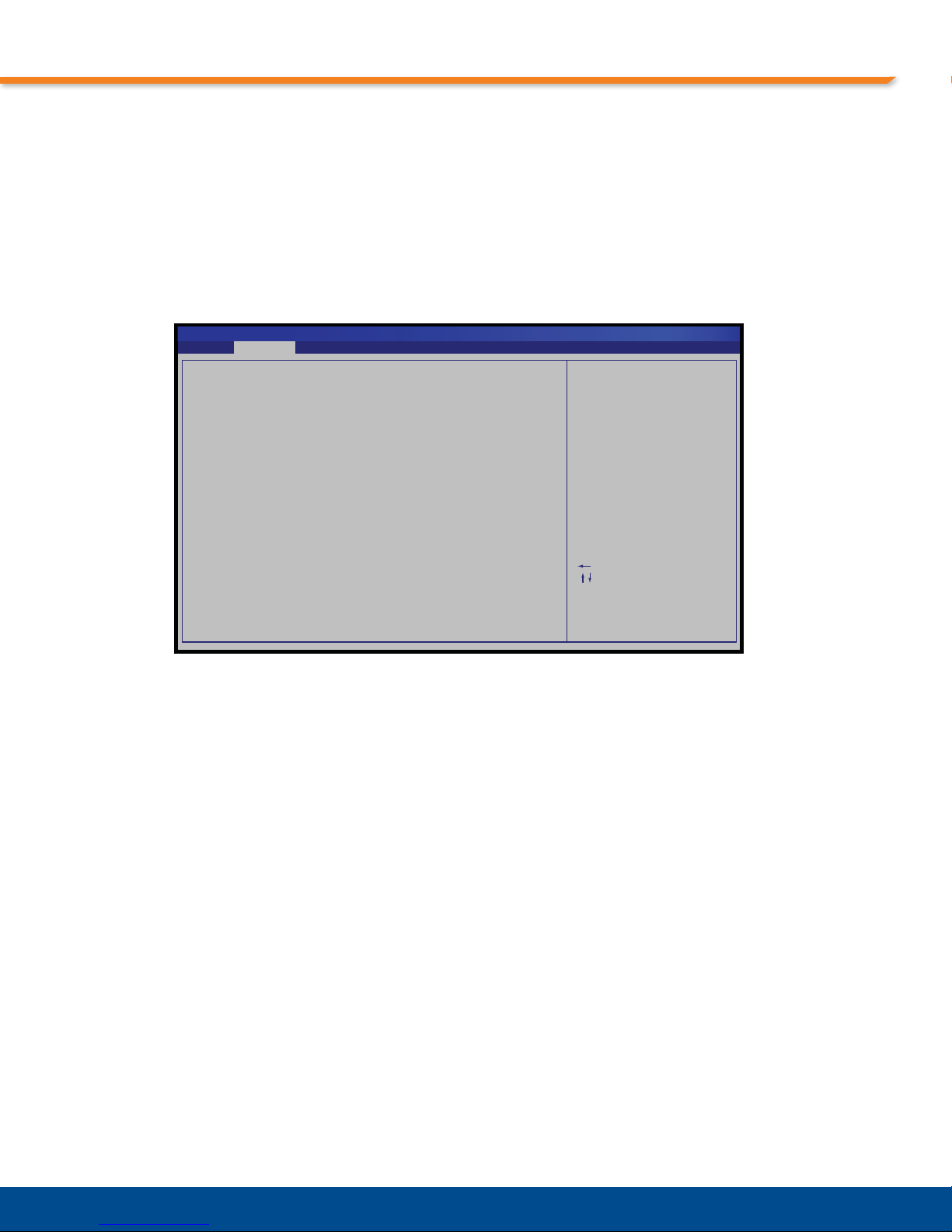
Chapter 3: Getting Started
BIOS SETUP UTILITY
Port Trunking Configuration
ESC
Save and Exit
Select Item
F10
General HelpF1
Enable/Disable
port trunking
Enter
Port Trunking
[Disabled]
Select Screen
Change Option
Exit
Advanced
Port Trunking Configuration
Port trunking allows using multiple Ethernet network ports in parallel to increase the link speed
beyond the limits of any one single port. The CPC5565 BIOS setup allows ena bling or disabling
of port trunking and the selection of a distribution algo rithm. Port trunking is disabled by default.
Selecting the Port Trunking Configuration option on the Switch Configuration submenu brings
up the screen shown in Figure 3-8 where this option can be configured.
Figure 3-8: Port Trunking Configuration Screen
Port trunking provides for higher bandwidth when the links are operational and it also provides
for link redundancy. If one link fails, the traffic is automatically moved to the other link. The onboard devices may be grouped in A/B pairs (ENET-A and ENET-B, or PMC-A and PMC-B,
etc.). Both of the trunked ports must be of the same speed.
By performing a dynamic hashing algorithm on the SA and/or DA MAC addresses, each p acket
destined for the trunk group is forwarded to one of the valid ports within the trunk group. This
method has several key advantages. By dynamically performing this function, the traffic
patterns can be balanced across the ports within a trunk. In addition, the MAC-based alg orithm
also provides dynamic fail-over . If a port within the trunk group fails, the other port automatically
assume all traffic designated for the trunk group. It allows for a seamless, automatic
redundancy scheme. This hashing function can be performed on the DA, SA, or DA and SA.
This mechanism does not involve the use of Link Aggregation Control Protocol (LACP). The
ports are statically configured as a two-port trunk. The device that connects to the CPC5565
must be compatible with this configuration.
46
Page 47
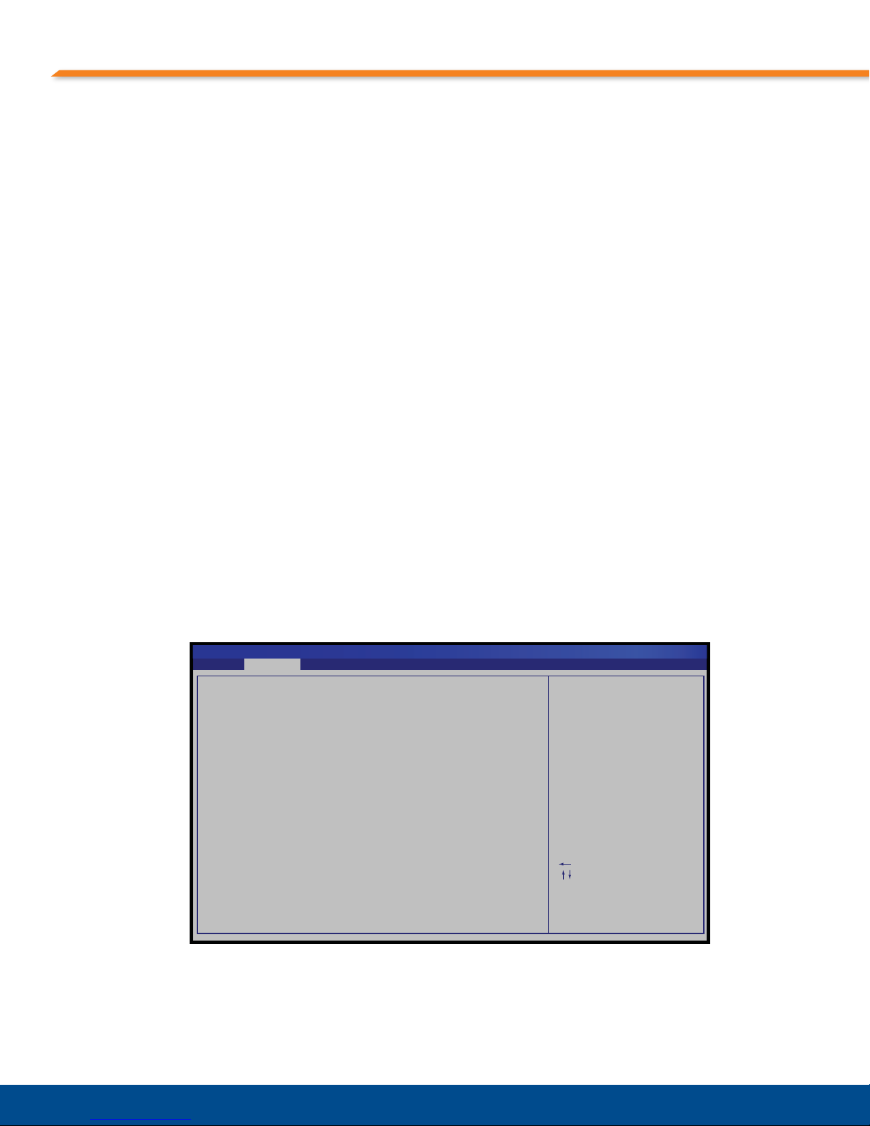
BIOS Configuration Overview
BIOS SETUP UTILITY
MAC Address Handling Configuration
ESC
Save and Exit
Select Item
F10
General HelpF1
Enabled = Allow switch
to learn source MAC
address.
Disabled = Disable
learning of MAC
addresses.
Enter
MAC Address Learning
Reserved Mcast Forward
[Enabled]
[Disabled]
Select Screen
Change Option
Exit
Advanced
MAC Address Handling Configuration
Selecting the MAC Address Handling Configuration option on the Switch Configuration
submenu brings up the screen shown in Figure 3-9, where the MAC handling options can be
configured.
The options for MAC Address handling include:
• Address learning enable or disable
• Reserved multicast forwarding enable or disable
Disabling address learning causes all packets received on a port to be forwarded to all other
ports in the ingress port's VLAN. This can be useful in network configurations where there is a
path for packets to flow from a port in one VLAN to a port in another VLAN. See “Network
Architecture Considerations,” on page 48. The default setting is to enable MAC address
learning.
Disabling reserved multicast forwarding causes the embedded switch to discard packets with
DA MAC addresses in the range of 01-80-C2-00-00-02 through 01-80-C2-00-00-0F. These
addresses are typically used for protocols such as:
• Link-Aggregation-Control-Protocol (LACP)
• 802.1x Port Authentication
• Multiple-VLAN-Registration-Protocol (MVRP)
• Link-Layer-Discovery-Protocol (LLDP)
If hosts attached to any of the ports of the embedded Ethernet switch particip ate in any of these
protocols and require packets to be sent through the embedded switch, then this option must
be set to forward these packets. The default configuration is to not forward these packets.
Figure 3-9: MAC Address Handling Configuration Screen
47
Page 48

Chapter 3: Getting Started
25
10GBASE-CX4 10GBASE-CX4
CONSOLE MGMT 10/100
SPD SPDLINK
CPC6620
LNK/ACT/SPD10G
25 1 2 3 4
5678
9101112
13 14 15 16
17 18 19 20
21 22 23 24
26
PWR
FLT
26
CompactPCI
R
CPC6620
FABRIC-A
25
10GBASE-CX4 10GBASE-CX4
CONSOLE MGMT 10/100
SPD SPDLINK
CPC6620
LNK/ACT/SPD10G
25 1 2 3 4
5678
9101112
13 14 15 16
17 18 19 20
21 22 23 24
26
PWR
FLT
26
CompactPCI
R
CPC6620
25
10GBASE-CX4 10GBASE-CX4
CONSOLE MGMT 10/100
SPD SPDLINK
CPC6620
LNK/ACT/SPD10G
25 1 2 3 4
5678
9101112
13 14 15 16
17 18 19 20
21 22 23 24
26
PWR
FLT
26
CompactPCI
R
CPC6620
FABRIC-B
P
M
C
CPC5565
BCM5389 SWITCH
PMC CPU
P
M
C
CPC5565
BCM5389 SWITCH
PMC CPU
ISL
Network Architecture Considerations
Typical co nfigurations that utilize the CPC5565 include two CPSB switch fabrics in the chassis.
The CPSB-A port of the CPC5565 connects to Fabric-A and the CPSB-B port of the CPC5565
connects to Fabric-B. The switch fabrics are often connected via an Inter-Switch Link (ISL).
See Figure 3-10.
Figure 3-10: Inter-Switch Link Connection
As can be seen from Figure 3-10, several potential sources of network loops exist. In order to
avoid these, a combination of VLAN configuration and Spanning Tree is required.
The CPC5565 does not participate in the Spanning Tree protocol, but most CPSB fabric
switches, including the PT-CPC6620, do. In order to allow STP devices to detect and block
loops, the BCM5389 switch on the CPC5565 is configured to pass STP Bridge Protocol Data
Units (BPDUs) between ports that are in common VLANs. Since the default VLAN
memberships place the fabric ports in separate VLANs, the default state of the switch is to
block Sp annin g Tree PDUs from flowing between these ports, but the separate VLANs prevent
broadcast storms.
Avoiding Loops
The primary methods to avoid network loops are:
• Create separate switching domains through wiring and/or VLAN management
• Use Spanning Tree
Separate Switching Domains
One solution to avoiding loops is to break the inter-switch link between the fabrics and create
separate traffic domains using VLAN management. In order to provide redundancy with this
configuration, the CPC5565 application software typically includes a high-availability protocol
such as:
48
Page 49
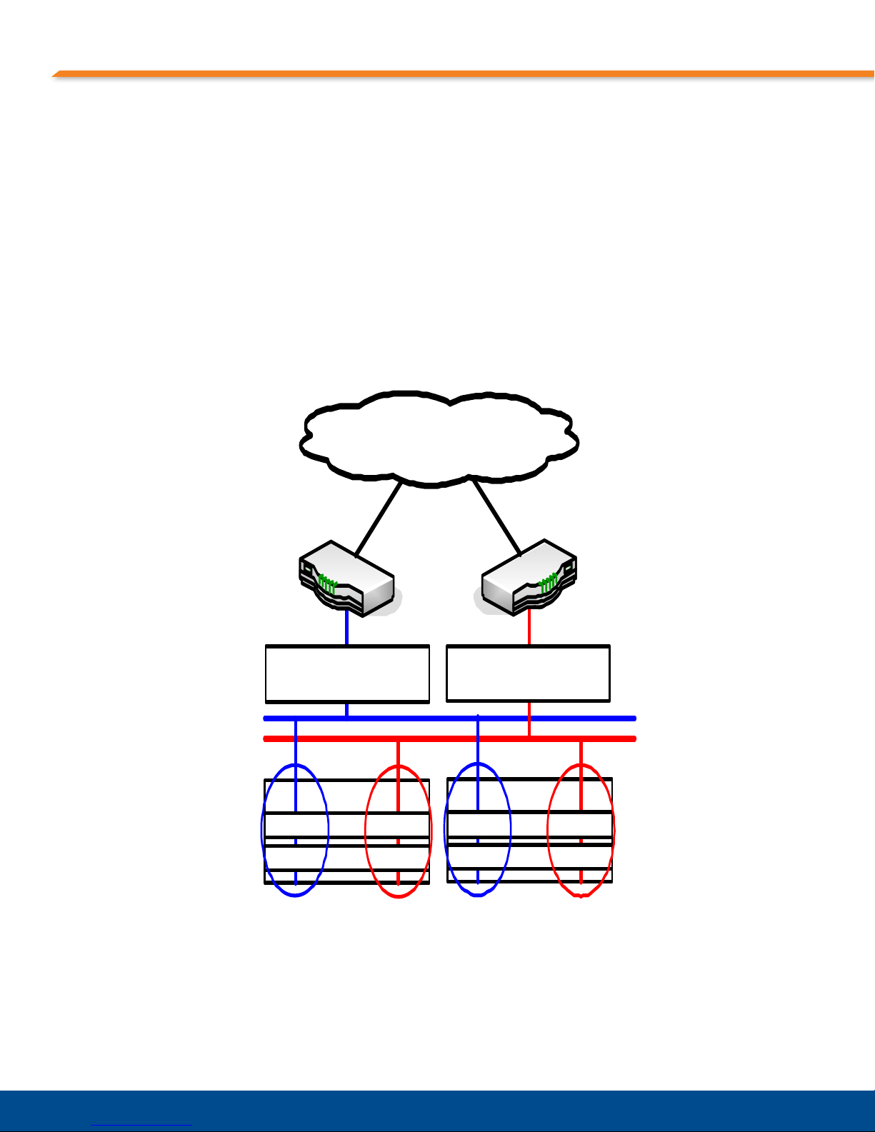
BIOS Configuration Overview
EXTERNAL NETWORK
vlan1
vlan2
FABRIC-A
CPC5565-A
CPSB-A CPSB-B
CPU
eth0
eth1
PMC
A
B
J9J8
FABRIC-B
CPC5565-B
CPSB-A CPSB-B
CPUeth0 eth1
PMC
A
B
J9J8
Router-A
Rout er-B
•SCTP
• Linux Bonding
• Solaris Multipathing.
These protocols allow for detection of a working path to an upstream resource such as a router ,
and then move a virtual IP address from a failed interface to a working interface.
Figure 3-11 illustrates this configuration. Two CPC5565 blades are connected via Fabric-A to
VLAN-1, which is connected to Router-A. These blades are also connected via Fabric-B to
VLAN-2, which is connected to Router-B. The Inter-Switch Link (ISL) between the fabrics is
disabled. For IP redundancy, the CPC5565 blades could use the Linux Bonding driver and
monitor the path to each router with ARPs and 'plumb' a Virtual IP Address onto the active
interface.
Figure 3-11: Separate Switching Domains
A similar H/A configuration can be achieved with this configuration using SCTP or Multipathing.
This technique can be used with or without tagged interfaces. To allow for tagged interfaces,
you must enable Port-Mode VLANs in the BIOS (see “Port VLAN Mode,” on page 44).
Untagged interfaces can be used with the default Dot1Q-Mode (see “802.1Q VLAN Mode,” on
page 43). Since there is no potential for a loop to form, Spanning Tree may be disabled on the
ports connected to the CPC5565.
49
Page 50
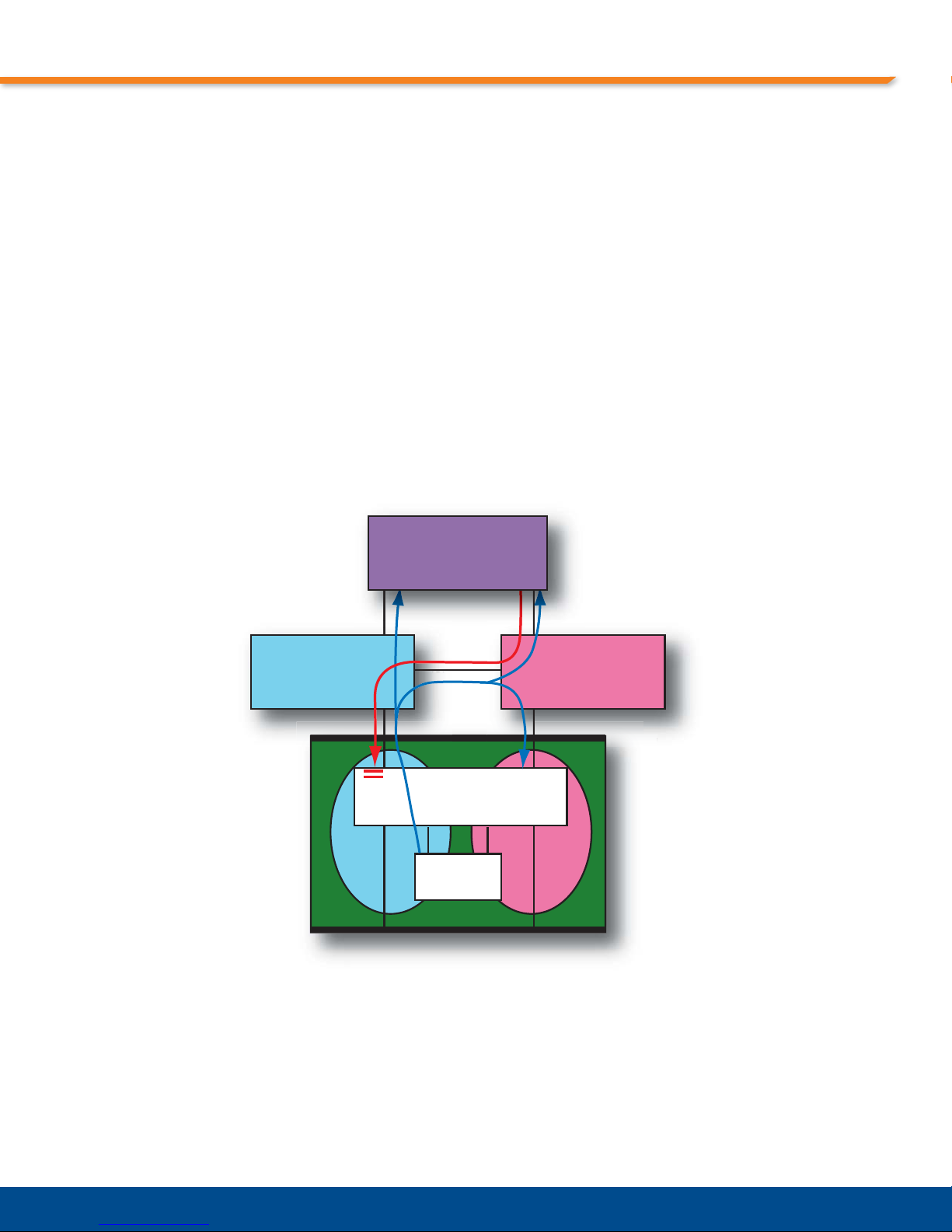
Chapter 3: Getting Started
Front Panel
Midplane
CPC5565
BCM5389
CPU
VLAN 1 VLAN 2
J8
ISL
eth0 eth1
J9
pla
Fabric-A Fabric-B
Host-A
eth0 eth1
Instead of disabling the link between the fabrics, the ISL could also be se gregated into a VLAN
that is not used for the CPC5565s.
If the network architecture segregates the ports into VLANs to prevent loops, but the re is a path
from one VLAN to the other, then an additional measure must be taken. While separation into
VLANs does prevent broadcast storms, having a path for packets between VLANs may cause
MAC address learning problems. This is illustrated in Figure 3-12.
The blue line illustrates a broadcast packet (eg. ARP) that is sent by the CPU's eth0 port. This
packet is sent through VLAN 1 on the embedded switch and forwarded to Host-A via the two
fabric switches. The packet is also sent back to the CPC5565 into VLAN 2 from Fabric-B. The
embedded switch sees the Source MAC address of eth0 and learns that MAC on the Fabric-B
port. If Host-A sends a packet (eg. ARP Reply) to that MAC address (red line), the fabric
switches deliver it to the CPC5565 on the correct port, but the embedded switch discards the
packet. This is because the target is a MAC that was learned in VLAN 2, but the ingress port is
in VLAN 1. This problem can be avoided by disabling MAC address learning. Refer to “MAC
Address Handling Configuration,” on page 47.
Figure 3-12: ISL Segregation and MAC Address Learning
Spanning Tree Redundancy
If you do not wish to include a high-availability protocol like:
•SCTP
• Linux Bonding
• Solaris Multipathing
neid
50
Page 51
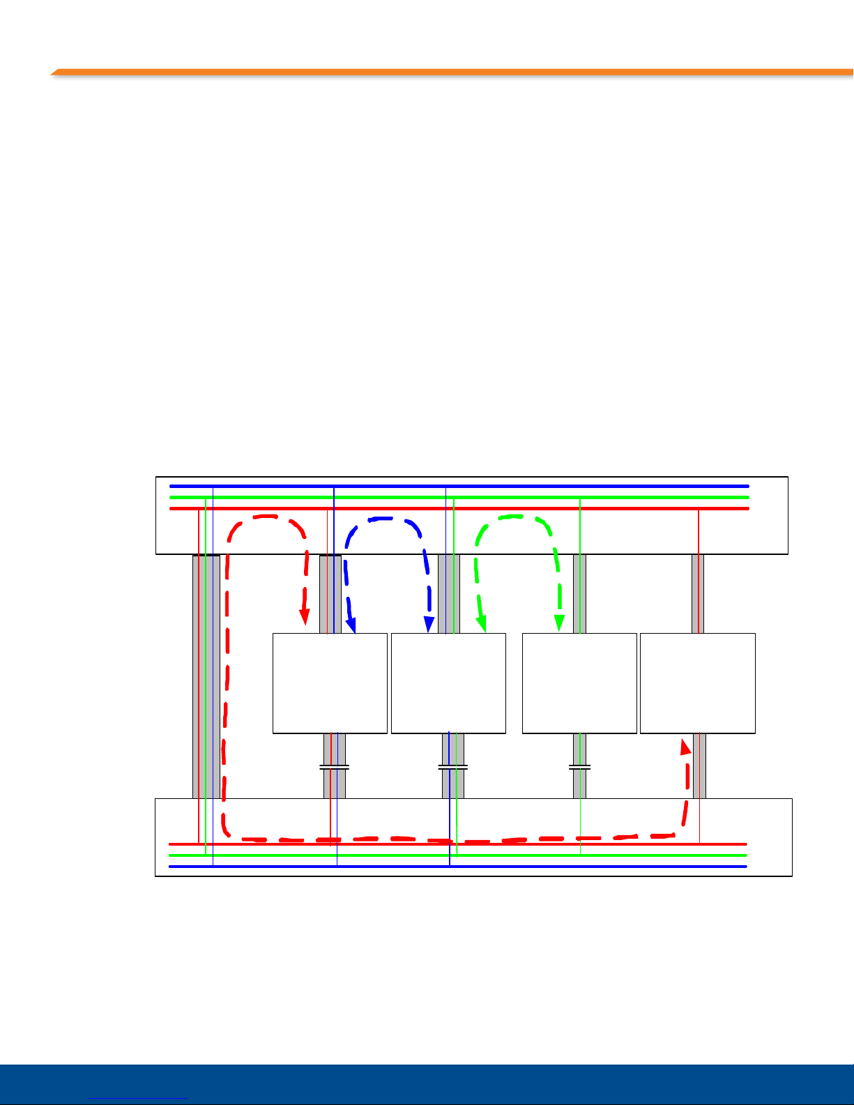
BIOS Configuration Overview
CPC5565-B
(VLA Ns 1, 2 )
CPSB-A
CPSB-B
VLAN 2 Switch
Port A
VLAN 3 Switch
Port A
Port B
FABRIC -A
vlan3
vlan2
vlan1
FABRIC -B
vlan3
vlan2
vlan1
CPC5565-A
(VLA Ns 1, 3 )
CPSB-A
CPSB-B
Port B
X
Cable Fault
BlockedBlockedBlocked
in your CPC5565 application software, then you may wish to provide redundancy through the
use of Spanning Tree on the fabrics. In this scenario, each CPC5565 has a path at layer-2 to
both fabrics by placing the CPSB ports into a common VLAN. This allows the fabrics to pass
Sp anning Tree BPDUs through the embedded switch on each CPC5565 and allows the fabrics
to block the redundant paths.
This technique can be used with or without tagged interfaces. To allow for tagged interfaces,
you must enable Port-Mode VLANs in the BIOS. Untagged interfaces can be used with the
default Dot1Q-Mode (see “VLAN Configurations,” on page 42).
Figure 3-13 illustrates an example where two CPC5565s are used in a network that has three
VLANs. The VLANs all use tagging. In order to support tagging, both CPC5565s are config ured
for Port-Mode VLANs. In order to support redundancy, redundant paths are provided via the
two fabric switches and Spanning Tree is utilized to create a loop-free topology.
In this example, two external Layer-2 switches are connected via fabric uplink ports. There is a
cable fault to the VLAN-3 switch so traffic to that device goes through Fabric-B. Otherwise, all
of the traffic flows through Fabric-A. Example traffic for each VLAN is illustrated with the colorcoded dashed lines.
Figure 3-13: Spanning Tree Redundancy
In addition to protecting the system against cable faults to external devices, this mode of
operation also protects the system against internal fabric faults. If Fabric-A fails, Fabric-B
unblocks all of the paths to the CPC5565s and the VLAN-2 switch and all traffic flows through
Fabric-B.
51
Page 52

Chapter 3: Getting Started
In order for Spanning Tree to function, BPDUs must pass between the CPSB-2.16 ports of
each CPC5565. Packets must be allowed to be switched between both eth0/eth1 interfaces
and both of the CPSB-2.16 ports. These requirements result in the need to place both CPU
Ethernet ports and both CPSB-2.16 ports into a common VLAN.
Console Redirection
Console redirection allows monitoring of the CPC5565's boot process and running the
CPC5565's BIOS setup utility from a remote serial terminal. Connection is made directly
through the front-panel console port. See “CPC5565 Front Panel,” on page 19, for the port
location.
The console redirection feature is most useful in cases where it is necessary to communicate
with the CPC5565 in an embedded application without video support.
Console redirection is configurable from the CPC5565's BIOS setup utility Remote Access
Configuration setup menu under the Advanced tab on the main menu. SW2-4 must also be
closed. See “SW2-4: Console Redirection,” on page 38.
The default CMOS settings within the Remote Access Configuration menu are as follows.
Remote Access: Enabled
Serial Port Number: COM1
Base Address, IRQ: 3F8h, 4
Serial Port Mode: 09600 8,n,1
Flow Control: None
Redirection After BIOS POST: Always
Terminal Type: VT100
VT-UTF8 Combo Key Support: Disabled
Sredir Memory Display Delay: No Delay
Note: Some operating systems may have problems with the redirection if BIOS POST is set to
Always. If there is a problem, try either the Disabled or Boot Loader options.
Older Operating Systems
For operating with older Operating Systems (such as Windows 2003 Server), in the BIOS Boot
Up Screen, select booting from Legacy IDE mode, not AHCI.
52
Page 53
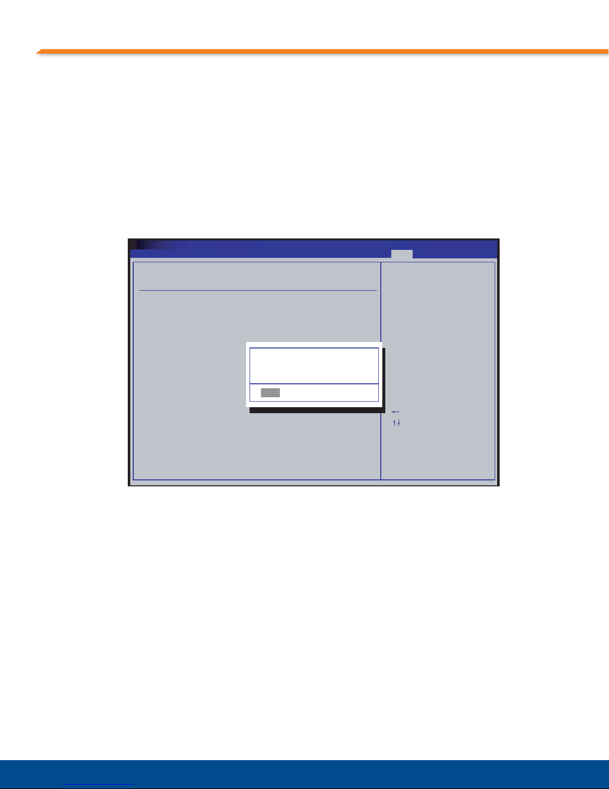
Custom Default Setup
BIOS SETUP UTILITY
Advanced Security Boot System Management Exit
Exit Options
Save Changes and Exit
Discard Changes and Exit
Discard Changes
Load Optimal Defaults
Save Custom Defaults
Save custom default
values for all the
setup questions.
Go to Sub ScreenEnter
Select Screen
Select Item
F1 General Help
F10 Save and Exit
ESC Exit
Main
Save custom defaults?
[Ok] [Cancel]
You can save configuration changes made in the BIOS setup as a custom default that is
reloaded, instead of the original default settings, if the system configuration image in CMOS is
corrupted. Because the custom default is saved in flash along with the BIOS image, the custom
default is erased if the BIOS image is updated.
To save your changes as a new custom default:
1. After making changes to the settings in the BIOS setup utility, arrow to the Exit menu (see Figure
3-14).
Figure 3-14: Saving Custom Defaults
BIOS Configuration Overview
2. Select Save Custom Defaults.
3. Press the Enter key. A popup window appears.
4. Select Ok and press the Enter key.
The popup window closes and the Exit menu changes to include two new options:
• Load Custom Defaults, used to restore your new custom settings.
• Clear Custom Defaults, used to clear your new custom default so the original, factory defaults are
used whenever CMOS is rewritten.
Behavior of the BIOS if a Corrupted CMOS Checksum is Detected
If the BIOS detects a corrupted checksum while booting, it continues to boot long enough to lo g
the error in the IPMI System Event Log. The BIOS then loads the default CMOS values and
resets the board in order to ensure that the correct CMOS values are used during the POST
operation. This feature is available beginning with BIOS version P02.
53
Page 54
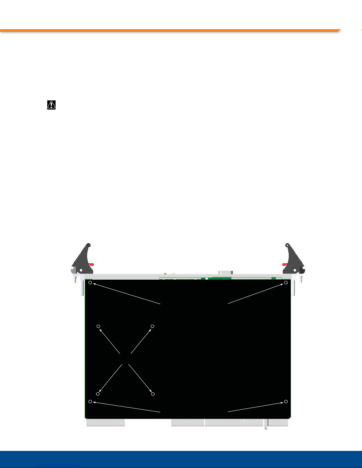
Chapter 3: Getting Started
Caution:
SHIELD FASTENER LOCATIONS
SHIELD FASTENER LOCATIONS
SATA FASTENER LOCATIONS
Installing a PMC Device
The following instructions are for mounting a PMC device on the CPC5565. This option is not
available if your CPC5565 was ordered with the SATA drive option. Refer to Figure 3-16, “PMC
Card Installation,” on page 56, when installing the PMC device.
Electronic components on printed circuit boards are extremely sensitive to static electricity.
Ordinary amounts of static electricity generated by your clothing or work environment can
damage the electronic equipment. We recommend using anti-static grounding straps and
anti-static mats to help prevent damage due to electrostatic discharge when installing the
PMC device.
Note:The PMC card must have transformers on it to provide proper isolation to the
CPC5565.
Note:The CPC5565 supports only 3.3V PMC cards.
1. Take the necessary precautions to protect from static discharge the PMC, CPC5565, and any other
devices you are working with.
2. If the CPC5565 includes a filler plate covering its PMC opening, remove it.
3. Remove the four shield fasteners and take off the black shield from the solder side of the board (see
Figure 3-15, “Solder-Side Shield” ).
Figure 3-15: Solder-Side Shield
54
Page 55

Installing a PMC Device
4. Lay the CPC5565 solder-side down on a flat surface covered with an anti-static mat.
5. Insert the PMC front panel into the CPC5565 front panel PMC opening.
6. Align the CPC5565 voltage key post with the correspondin g ho le in th e PMC.
7. Align the PMC device's PMC connectors with the CPC5565 PTMC connectors and press together
until the connectors are completely engaged.
8. After the PMC connectors are properly seated, check that the PMC device st andoff s are flush with the
appropriate holes on the CPC5565.
9. Insert screws through the CPC5565 and into the standoffs.
10.Tighten screws to 2 to 4 in/lbs.
11.If appropriate, reattach the solder-side cover to the CPC5565.
55
Page 56
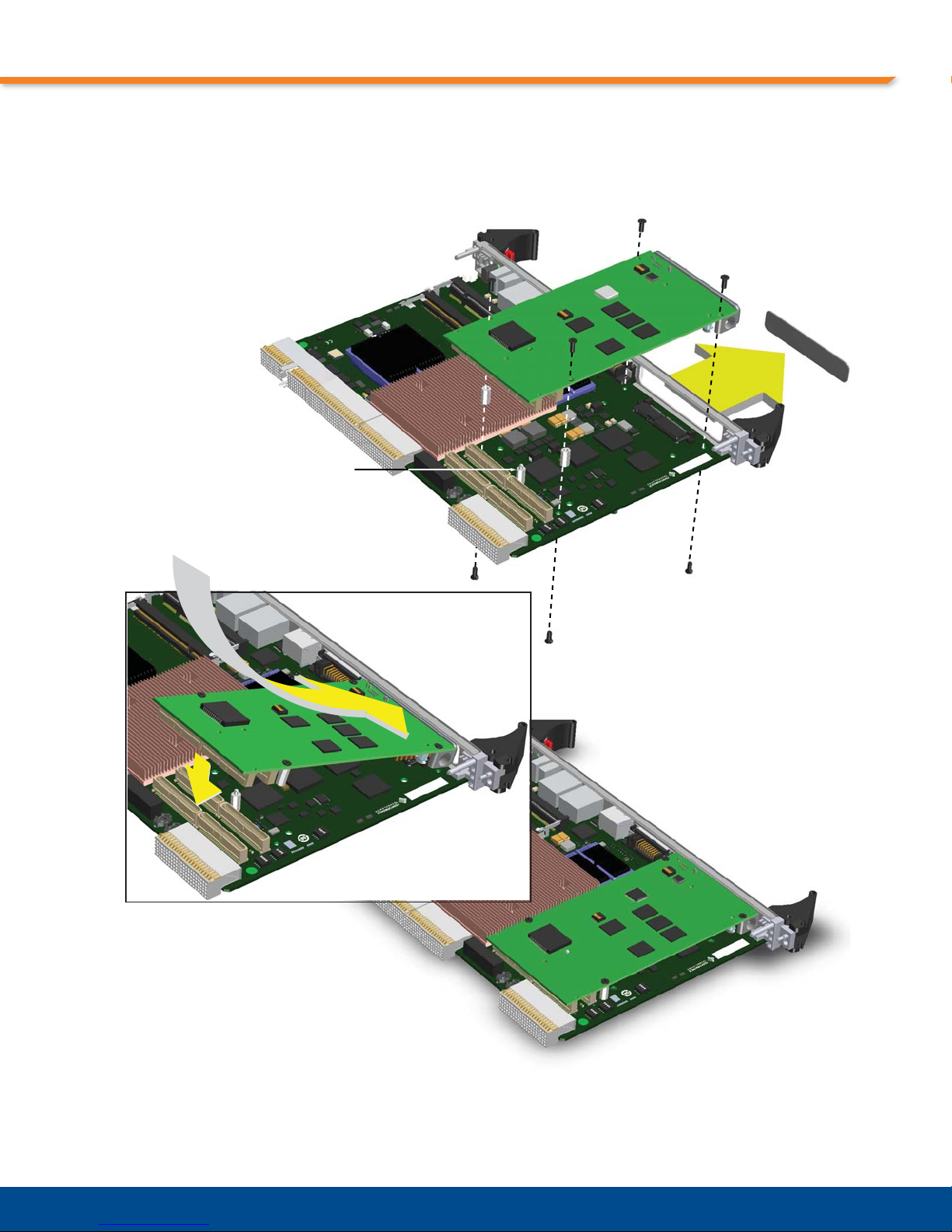
Chapter 3: Getting Started
Voltage Key Post
Figure 3-16: PMC Card Installation
56
Page 57

Installing the Operating System
For more detailed information about your operating system, refer to the documentation
provided by the operating system vendor and to the PT Web site.
To install the operating system:
1. Install peripheral devices. CompactPCI devices are automatically configured by the BIOS during the
boot sequence.
2. Most operating systems require initial installation on a hard drive from a USB CD/DVD or PXE. These
devices should be configured, installed, and tested with the supplied drive rs before attempting to load
the new operating system.
3. Read the release notes and installation documentation provided by the operating system vendor. Be
sure to read any readme files or documents provided with the OS as these typically note
documentation discrepancies or compatibility problems.
4. Select the appropriate boot device order in the setup boot menu depending on the OS installation
media used. To boot from a USB CD-ROM, first connect the USB drive, then enter the BIOS setup
utility and move the “CD-ROM” device to the top of the boot list (or above any other bootable
devices).
Installing the Operating System
5. Proceed with the OS installation as directed, being sure to select appropriate device types if
prompted. Refer to the appropriate hardware manuals for specific device types and compatibility
modes of PT products. A link to PT manuals is available in the topic “User Documentation,” on page
117.
6. When installation is complete, reboot the system and set the boot device order in the setup boot
menu.
Note: For more information about the BIOS setup utility, see the topic “BIOS Configuration
Overview,” on page 40.
USB CD/DVD
Note: Win XP and Red Hat Enterprise Linux AS 4 Update 3 (AMD64/Intel EM64T) have been
validated for this installation (pending).
To run the BIOS setup utility with a bootable OS installation CD or DVD in an external USB
drive:
1. Cable an external USB CD/DVD drive to the USB port on the CPC5565.
2. Ensure the USB CD/DVD drive is powered on.
3. Insert the bootable OS installation CD/DVD into the drive.
4. Run the CPC5565 BIOS setup utility by pressing the F2 key while the SBC is booting up.
5. Ensure that the USB device is listed in the Boot Devices and is above any other device that may have
a bootable OS image (i.e. hard drive).
a. Use the right arrow key to highlight the Boot category in the setup menu. The Boot Settings
information appears in the main setup screen.
b. Arrow down to Boot Device Priority and press <Enter>. The boot or de r list ap pe a rs an d the top
position in the boot order is highlighted.
57
Page 58

Chapter 3: Getting Started
c. Press <Enter>. A dialogue box with a list of boot devices appears.
d. Arrow up or down to highlight the USB d evice. Pre ss <Enter>. USB appear s at the top of the Boo t
Device Priority list.
e. Press <Esc> to exit to the main menu.
f. Right arrow to select the Exit menu item. Save Changes and Exit is highlighted.
g. Press <Enter>. OK is highlighted.
6. Press <Enter> to exit the BIOS setup utility.
PXE
The CPC5565 BIOS settings default to loading and initializing the PXE Option ROM. If this
feature is not to be used, the BIOS settings can be changed so the PXE Option ROM is not
loaded. This speeds the BIOS boot sequence. The PXE Option ROM can be disabled in the
PCI/PnP menu.
Creating a bootable PXE OS or installing an OS over PXE is beyond the scope of this manual.
Operating Systems Supported
WinXP and WinXP 64 have been installed and run through Microsoft's Hardware Compatibility
Test (HCT) successfully (pending).
Solaris 10 has been installed successfully. Upon successful completion of Sun Hardware
Compatibility Test Suite (HCTS), results will be posted to Sun's Web page http://www.sun.com/
bigadmin/hcl/overview.html.
Red Hat Enterprise Linux AS 4 Update 3 (32 and 64 bit versions) has been installed
successfully (pending). Upon successful completion of Red Hat Enterprise Certification Test
Suite, the results will be posted on the Red Hat Web site http://hardware.redhat.com.
58
Page 59
Programming the LEDS
The CPC5565 includes one user-controlled, bicolor (yellow/green) LED located on the front
panel. See Figure 2-1, “CPC5565 Front Panel,” on page 19. The user LED is software
programmable through GPIO bits 24 and 25 of the Intel 3100 GPIO_USE_SEL1 register
(500h). The LED is turned off after a power cycle or a reset.
As shown below, two bits each are used to control the state of the user LED. Since a bicolor
LED is used, there are four states for the LED: yellow , green, both colors of f and both colors on.
Bit Yellow Green Both Off Both On
Bit 24 0 1 1 0
Bit 25 1 0 1 0
The GPIO bits that control the user LED's bits are in the same register as other system critical
functions. It is important not to change the state of other bits in this register when modifying the
user LED status. The register address used to change the level of GPIO bits 0 - 31 is 50Ch.
Care should be taken to read a double word from this register and change only bits 24 and 25
to the desired values, then write the double word back out to IO address 50Ch, preserving all
other bits in the double word.
Programming the LEDS
S T A T E
Installing the Display Drivers
The AMD/ATI Radeon E2400 video processor on the CPC5565 requires the installation of the
AMD display drivers and software for the appropriate operating system.
Before proceeding, go to the AMD support Web site to download the most current version of
the display drivers for the appropriate operating system. Driver installation is operating system
dependent and may vary depending on the operating system installed.
To download the display drivers:
1. Go to http://ati.amd.com/support/driver.html
2. Select the desired operating system in the first column.
3. Select Embedded in the second column.
4. Select E2400 in the third column.
5. Click Go.
6. Click the Download Link to download the drivers.
Refer to the Driver Release Notes and Installation Instructions for your operating system at the
AMD support Web site for more information. The following sections describe how to install the
AMD display driver.
59
Page 60

Chapter 3: Getting Started
Windows XP (32- and 64-Bit Editions)
1. Install the operating system (see “Installing the Operating System,” on page 57).
2. Activate and install any Windows XP update patches for the given operating system.
3. It is highly recommended that you disable any antivirus, anti-spyware, or any other system protection
software before continuing.
4. Prior to installing the AMD Catalyst™ Control Center software suite for the AMD/ATI Radeon E2400
video processor , which allows you to control the configuration of the video device, you must install
Microsoft .NET™ Framework version 2.0. You can verify that you have the .NET Framework by
checking in the Add/Remove Programs list in the Control Panel. If the .NET Framework is not listed,
download and install it before proceeding. Refer to http://www.microsoft.com/downloads.
Note: Installing the Catalyst Control Center and Microsoft .NET Framework 2.0 allows
optimal configuration of the CPC5565 under Windows XP operating systems.
5. Create a separate directory on the system hard disk drive and extract the AMD driver files into that
directory.
6. Double click the setup.exe file for the driver software.
Linux
Solaris
7. Follow the directions on the Setup windows to install the Audio, Video and Catalyst Control Center
software. Select the Express Installation for the easiest setup.
8. After all software is installed you are prompted to restart your system for the installation changes to
take effect.
9. After restarting the system the display driver installation is complete.
1. Install the operating system (see “Installing the Operating System,” on page 57).
2. Refer to the AMD support Web site at http://ati.amd.com/support/driver.html to download the display
driver and to find installation instructions for Linux.
Contact Sun Microsystems for information about the display drivers for Solaris operating
systems.
60
Page 61

Chapter 4
System Monitoring and Alarms
The CPC5565 performs system monitoring and alarming functions using the flexible, industry
standard, Intelligent Platform Management Interface (IPMI). The CPC5565 comes equipped
with an on-board Intelligent Platform Management Controller (IPMC) chip, IPMI and IPMB Jconnector pinouts, and IPMC firmware already installed on the board. The IPMC firmware is
based on Pigeon Point System's (PPS) MMC firmware.
Key topics in this chapter include:
• “IPMC Functions,” on page 61
• “Summary of Supported Commands,” on page 62
• “Device Locator Record,” on page 64
• “Sensors,” on page 66
• “Serial Interface Subsystem,” on page 68
• “Firmware Upgrade Process,” on page 76
IPMC Functions
Some of the functions available on the module through the IPMI interface include:
• Monitoring of the CPU and board temperatures with critical and non-critical alerting
• Monitoring of the voltage rails with critical and non-critical alerting
• Remote reset and shutdown of the module (hard and soft)
• Monitoring of ejector switches for hot-swap functionality (PT’s NexusWare IPMI driver and firmware
provide additional payload features for hot swap)
• Monitoring and event reporting of critical errors
• Interface to IPMB
In order to take advantage of the features provided by the firmware, IPMI-aware applications
must be developed. Information on IPMI v1.5 is provided at:
http://www.intel.com/design/servers/ipmi/spec.htm
61
Page 62

Chapter 4: System Monitoring and Alarms
Summary of Supported Commands
Table 4-1, “IPMI/PICMG Command Subset Supported by the IPMC Firmware,” lists all the
commands supported by the IPMC.
The Spec Re f column indicates where in the relevant specification a command is defined. IPMI
references are to v1.5 unless indicated otherwise. The IPMC Req column indicates if a
particular command is required by the relevant specification (AMC Specification or HPM.1
Specification) or is optional.
See the various notes under the table for more information.
Table 4-1: IPMI/PICMG Command Subset Supported by the IPMC Firmware
Command Spec Ref NetFn CMD
IPM Device “Global” Commands
Get Device ID 17.1 App 01h
Cold Reset 17.2 App 02h
Warm Reset 17.3 App 03h
Broadcast “Get Device ID”
a
Messaging Commands
Set BMC Global Enables 18.1 App 2Eh
Get BMC Global Enables 18.2 App 2Fh
Clear Message Flags 18.3 App 30h
Get Message Flags 18.4 App 31h
Get Message 18.6 App 33h
Send Message 18.7 App 34h
BMC Watchdog Timer
Reset Watchdog Timer 21.5 App 22h
Set Watchdog Timer 21.6 App 24h
Get Watchdog Timer 21.7 App 25h
Event Commands
Set Event Receiver 23.1 S/E 00h
Get Event Receiver 23.2 S/E 01h
Platform Event (a.k.a. “Event Message”) 23.3 S/E 02h
Sensor Device Commands
Get Device SDR Info 29.2 S/E 20h
Get Device SDR 29.3 S/E 21h
Reserve Device SDR Repository 29.4 S/E 22h
Get Sensor Reading Factors 29.5 S/E 23h
Set Sensor Hysteresis 29.6 S/E 24h
Get Sensor Hysteresis 29.7 S/E 25h
Set Sensor Threshold 29.8 S/E 26h
Get Sensor Threshold 29.9 S/E 27h
Set Sensor Event Enable 29. 10 S /E 28h
17.9 App 01h
62
Page 63

Summary of Supported Commands
Table 4-1: IPMI/PICMG Command Subset Supported by the IPMC Firmware (Continued)
Command Spec Ref NetFn CMD
Get Sensor Event Enable 29.11 S/E 29h
Get Sensor Event Status 29.13 S/E 2Bh
Get Sensor Reading 29.14 S/E 2Dh
FRU Device Commands
Get FRU Inventory Area Info 28.1 Storage 10h
Read FRU Data 28.2 Storage 11h
Write FRU Data 28.3 Storage 12h
AdvancedTCA Commands
Get PICMG Properties 3-10 PICMG 00h
FRU Control 3-25 PICMG 04h
FRU Control Capabilities 3-24 PICMG 1Eh
Get FRU LED Properties 3-27 PICMG 05h
Get LED Color Capabilities 3-28 PICMG 06h
Set FRU LED State 3-29 PICMG 07h
Get FRU LED State 3-30 PICMG 08h
Get Device Locator Record ID
b
3-35 PICMG 0Dh
HPM.1 Upgrade Commands (HPM.1)
Get Target Upgrade Capabilities 3-3 PICMG 2Eh
Get Component Properties 3-5 PICMG 2Fh
Abort Firmware Upgrade 3-15 PICMG 30h
Initiate Upgrade Action
c
Upload Firmware Block 3-9 PICMG 32h
Finish Firmware Upload 3-10 PICMG 33h
Activate Firmware 3-11 PICMG 35h
Query Self-Test Results
Query Rollback Status
Initiate Manual Rollback
a. See “Device ID” below, for the device ID data retrieved in response to a (Broadcast) Get
Device ID command for this module.
b. See “Device Locator Record” below, for the IPMB management controller device locator re-
cord retrieved in response to a Get Device Locator Record ID command for this module.
c. The HPM.1 Initiate Upgrade Action command is mandatory for an IPM Controller indicat-
ing that any of its implemented components supports preparation for Firmware Upgrade or
comparison of the current firmware
d. The HPM.1 Query Self-test Results command is mandatory for IPM Controllers indicating
self-test is supported in the Self-test capabilities field of the “Get target upgrade capabilities”
response or the Self-test capabilities field of the Upgrade Image header.
e. The HPM.1 Query Rollback Status command is mandatory for IPM Controllers supporting
automatic or manual Rollback.
f. The HPM.1 Manual Firm ware Rollback command is mandatory for IPM Controllers indi-
cating manual firmware Rollback is supported in the Manual firmware Rollback capabilities
field of the “Get target upgrade capabilities” response.
d
e
f
3-8 PICMG 31h
3-12 PICMG 36h
3-13 PICMG 37h
3-14 PICMG 38h
63
Page 64

Chapter 4: System Monitoring and Alarms
Device Locator Record
The IPMC firmware supports the Get Device Locator Record ID command for FRU device #0
(the only FRU device represented by an IPMC). The IPMC firmware obtains the ID of the IPMB
management controller device locator record by scanning the SDR records embedded into the
firmware.
Table 4-2 shows an example of an IPMB management controller device locator record (SDR
type 0x12) describing the properties of the IPMC:
Table 4-2: IPMB Management Controller Device Locator Record
Parameter Value
Power State Notification
ACPI System Power State notification required NO
ACPI Device Power State notification required NO
Global Initialization
Controller logs Initialization Agent errors NO
Log Initialization Agent errors accessing this
controller
Event Generation Enable event message generation from controller
Device Capabilities
Chassis Device NO
Bridge NO
IPMB Event Generator YES
IPMB Event Receiver NO
FRU Inventory Device YES
SEL Device NO
SDR Repository Device NO
Sensor Device YES
FRU Entity ID 0x07
Entity Instance (slot dependent)
OEM-specific 0
Device ID String Type/Length 8-bit ASCII with size of Device ID String (see below)
Device ID String CPC5565
NO
64
Page 65

Device ID
The IPMC firmware provides the following device ID data in response to the (Broadcast) Get
Device ID command:
Table 4-3: IPMC Device ID
Parameter Value
Device ID 0x00
Provides Device SDRs YES
Device Revision Number 0x00
Device Available YES
Firmware Revision Changes with each release
IPMI Version 1.5
Additional Device Support
Chassis Device NO
Bridge NO
IPMB Event Generator YES
IPMB Event Receiver NO
FRU Inventory Device YES
SEL Device NO
SDR Repository Device NO
Sensor Device YES
Manufacturer ID 0x000614
Product ID 0x5565
Auxiliary Firmware Revision Information 0x00000000
Device Locator Record
65
Page 66

Chapter 4: System Monitoring and Alarms
Sensors
Table 4-4 lists the sensors that are monitored by the IPMC. Note that the sensor IDs are local to
the IPMC.
Table 4-4: IPMC Sensors
Lower NonSensor ID
0 Hot Swap N/A N/A N/A N/A N/A N/A
1 1.5V N/A 1.40V 1.42V 1.58V 1.6V N/A
2 3.3V N/A 2.97V 2.99V 3.57V 3.59V N/A
3 VCC_CPU N/A 0.69V 0.72V 1.38V 1.41V N/A
4 3.3V IN N/A 2.97V 2.99V 3.57V 3.59V N/A
5 1.05V N/A 0.98V 1.0V 1.1V 1.12V N/A
6 1.8V N/A 1.68V 1.70V 1.90V 1.92V N/A
7 1.2V N/A 1.12V 1.14V 1.26V 1.28V N/A
8 5V IPMB N/A 4.5V 4.54V 5.47V 5.49V N/A
9 VIO N/A 2.97V 2.99V 5.47V 5.49V N/A
10 0.9V N/A 0.81V 0.855V 0.945V 0.99V N/A
1 1 2.5V N/A 2.38V 2.39V 2.56V 2.57V N/A
12 1.8V MEM N/A 1.72V 1.74V 1.86V 1.88V N/A
13 1V N/A 0.87V 0.88V 1.12V 1.13V N/A
14 5V N/A 4.5V 4.54V 5.47V 5.49V N/A
15 1.1V N/A 1.02V 1.04V 1.16V 1.18V N/A
16 5V IN N/A 4.5V 4.54V 5.47V 5.49V N/A
17 POWER GOOD N/A N/A N/A N/A N/A N/A
18 CPU ERROR N/A N/A N/A N/A N/A N/A
19 THERM TRIP N/A N/A N/A N/A N/A N/A
20 BMC Watchdog N/A N/A N/A N/A N/A N/A
21 Version Change N/A N/A N/A N/A N/A N/A
22 CPU TEMP -5C 0C 5C 80C 100C 110C
23 VIDEO TEMP -5C 0C 5C 90C 100C 110C
24 DIMM2 TEMP
25 DIMM TEMP -5C 0C 5C 65C 85C 95C
Description
(when present)
Recover-
able
Threshold
-5C 0C 5C 65C 85C 95C
Lower
Critical
Threshold
Lower NonCritical
Threshold
Upper NonCritical
Threshold
Upper
Critical
Threshold
Upper NonRecoverable
Threshold
66
Page 67

Interpreting Sensor Events
PT adopts the following philosophy with respect to threshold sensor event severity levels:
• Non-critical:
A warning that things are somewhat out of normal range, but not really a “problem” yet
•Critical:
Things are still in valid operating range, but are getting close to the edge; unit still operating within
specified tolerances.
• Non-recoverable:
Unit no longer operating within specified tolerances
Non-critical events are informative only - they do not indicate that the board is outside of its
operating limits. In general, no action is required. However, in certain contexts, system/shelf
management software may decide that preventive action should be taken. For example, if
several boards in a shelf report upper non-critical temperature events , the shelf manager might
decide to increase fan speed.
Critical events indicate that the board is still within its operating limits, but it is close to
exceeding one of those limits. Possible action in this case is to closely monitor the alarming
sensor and take more aggressive action if it approaches the non-recoverable threshold.
Sensors
Non-recoverable events indicate that the board may no longer be functioning because it is now
outside of its operating limits. It is likely that action is required o r has already b een t aken by the
local hardware/firmware. For example, a processor may have shut itself down because its
maximum die temperature was exceeded, or a shelf manager may decide to deactivate the
board because the processor is too hot.
67
Page 68

Chapter 4: System Monitoring and Alarms
Serial Interface Subsystem
The IPMC firmware implements a communication protocol over the payload and/or serial
debug interfaces. The communication is in the form of formatted ASCII strings.
The Serial Interface Protocol Lite (SIPL) is based on the IPMI-defined Terminal Mode of the
serial/modem interface. The following sections describe the SIPL:
• “Terminal Mode Messages and Commands,” on page 68
• “Terminal Mode Line Editing,” on page 69
• “Supported PPS Extension Commands,” on page 70
Terminal Mode Messages and Commands
Terminal Mode Message Format
Terminal Mode messages have the following format:
[<message data>]<newline>
The left bracket and the right bracket plus <newline> characters serve as START and STOP
delimiters for a message. The IPMC does not support multi-line IPMI messages.
Raw IPMI Messages
The SIPL supports raw IPMI messages that are entered as sequences of case-insensitive hexASCII pairs, each pair optionally separated from the previous one with a single <space>
character. What follows are examples of raw IPMI request messages in Terminal Mode:
[18 00 22]<newline>
[180022]<newline>]
The IPMC handles raw IPMI messages in the same way as it handles IPMI/PICMG/AMC
messages coming from the IPMB bus and, with the exception that IPMI/PICMG/AMC replies
are routed to the interfaces from which the respec tive requests have co me (i.e. either the serial
debug or payload interface of the IPMC).
Terminal Mode Text Commands
The SIPL does not support Terminal Mode ASCII text commands defined by the IPMI
Specification (section 13.7.8).
68
Page 69

Serial Interface Subsystem
[B8 00 01 0A 40 00 12]
Data
PPS IANA
Command Code
rqSeq (00h) / Bridge (00b)
NetFn Code (2Eh) / LUN (00b)
[BC 00 01 00 0A 40 00 34]
Data
PPS IANA
Completion Code
Command Code
rqSeq (00h) / Bridge (00b)
NetFn Code (2Eh) / LUN (00b)
Pigeon Point Systems (PPS) Extension Commands
The IPMC firmware supports a set of PPS extension commands that are used to control and
monitor the Intelligent Platform Management Controller (IPMC) state over the serial debug
interface. These commands are used to read the IPMC status, implement graceful payload
shutdown, etc.
The PPS extension commands are implemented as OEM IPMI commands with network
function codes 2Eh/2Fh and message body transferred in the same manner as for raw IPMI
messages (see “Raw IPMI Messages,” on page 68). Figure 4-1, “PPS Extension Command
Request,” shows an example of a PPS extension command request:
Figure 4-1: PPS Extension Command Request
Figure 4-2, “PPS Extension Command Response,” shows an example of a PPS extension
command response:
Figure 4-2: PPS Extension Command Response
Terminal Mode Line Editing
The IPMC does not support input line editing functionality defined as optional in the IPMI
Specification (section 13.8).
69
Page 70

Chapter 4: System Monitoring and Alarms
Supported PPS Extension Commands
The IPMC firmware supports the following PPS extension commands (see “Pigeon Point
Systems (PPS) Extension Commands,” on page 69):
Table 4-5: PPS Extension Commands Supported by the IPMC
Command
Request/Response
Get Status 0x00 Serial debug and
Get Serial Interface
Properties
Set Serial Interface
Properties
Get Debug Level 0x03 Serial debug
Set Debug Level 0x04 Serial debug
Get Payload
Communication
Timeout
Set Payload
Communication
Timeout
Graceful Reset 0x11 Payload interface The payload is ready
Diagnostic Interrupt
Results
Get Payload
Shutdown Timeout
Set Payload
Shutdown Timeout
Get Geographic
Address
Code
0x01 Serial debug and
0x02 Serial debug and
0x09 Serial debug and
0x0A Serial debug and
0x12 Payload interface Return diagnostic
0x15 Serial debug and
0x16 Serial debug and
0x2C Serial debug and
Likely Command
Source(s)
payload interfaces
payload interfaces
payload interfaces
interface
interface
payload interfaces
payload interfaces
payload interfaces
payload interfaces
payload interfaces
Description See Also
Read the IPMC status Get Status Command
Get the properties of a
serial interface Serial Line Properties
Set the properties of a
serial interface
Get debug/verbosity
level Debug/Verbosity Level
Set debug/verbosity
level
Get the timeout for
payload
communications
Set the timeout for
payload
communications
to be shut down/reset
interrupt results
Get the timeout for
payload shutdown Paylo ad Shutdown
Set the timeout for
payload shutdown
Get the geographic
address
Commands
Payload
Communication
Timeout
Graceful Payload
Reset
Payload Diagnostic
Interrupt
Timeout
Get Geographic
Address Command
The IPMC accepts all PPS extension commands listed in Table 4-5 from both serial interfaces,
as well as IPMB. This is done to achieve additional flexibility and extensibility in the IPMC
functionality.
The PPS extension commands listed in Table 4-5 are referred to as the SIPL commands
throughout this document. The following sections discuss the SIPL commands in more detail.
70
Page 71

Serial Interface Subsystem
Get Status Command
The IPMC status is four bytes describing the logical state of the IPMC and the payload. Table
4-6, “IPMC Status Bits,” provides a description of the IPMC status bits:
Table 4-6: IPMC Status Bits
Bit Name Description
Byte 1
0 (LSB) Control If set to 0, the IPMC control over the payload is disabled.
1-2 NA Reserved
3 Sensor Alert If set to 1, indicates that at least one of the IPMC sensors detects
threshold crossing.
4 Reset Alert If set to 1, indicates that the payload is going to be reset.
5 Shutdown Alert If set to 1, indicates that the payload is going to be shut down.
6 Diagnostic Interrupt
Request
7 (MSB) Graceful Reboot
Request
Byte 2
0-7 NA Reserved
Byte 3
0-7 NA Reserved
Byte 4
0-3 NA Reserved
4 Message Received If set to 1, indicates that a message for the payload has been received.
5-7 NA Reserved
If set to 1, indicates that a payload diagnostic interrupt request has
arrived.
If set to 1, indicates that the payload is requested to initiate the graceful
reboot sequence.
The IPMC firmware notifies the payload about changes of all status bits except for bits 0-2 of
byte 1 by sending an unprintable character (ASCII 07, BELL) over the payload interface. The
payload is expected to use the Get S tatus co mmand to identify pending events and other SIPL
commands to provide a response (if necessary). The event notification character is sent in a
synchronous manner, and does not appear in the contents of SIPL messages sent to the
payload.
The Get Status command has the following synopsis:
[B8 xx 00 0A 40 00]
The IPMC responds to the Get Status command with the following reply:
[BC xx 00 00 0A 40 00 <byte1> <byte2> <byte3> <byte4>]
71
Page 72

Chapter 4: System Monitoring and Alarms
Serial Line Properties Commands
The SIPL provides commands to get/set the properties of the IPMC serial inter faces (the se rial
debug interface and the payload interface):
• “Get Serial Interface Properties Command,” on page 72
• “Set Serial Interface Properties Command,” on page 72
Get Serial Interface Properties Command
The Get Serial Interface Properties command is used to get the properties of a particular
serial interface. This command has the following synopsis:
[B8 xx 01 0A 40 00 <interface ID>]
The <interface ID> parameter can have one of the values shown in Table 4-7, “The
<interface ID> Parameter Values,” below.
Table 4-7: The <interface ID> Parameter Values
Interface ID Description
0 Serial debug interface
1 Payload interface
The IPMC responds to the Get Serial Interface Properties command with the following reply:
[BC xx 01 00 0A 40 00 <interface properties>]
The <interface properties> parameter has the bit fields shown in Table 4-8, “The
<interface properties> Parameter Bit Fields,” below.
Table 4-8: The <interface properties> Parameter Bit Fields
Bits Name Description
0-3 Baud Rate ID The baud rate ID defines the interface baud rate as
follows:
0 – 9600 bps
1 – 19200 bps
2 – 38400 bps
3 – 57600 bps
4 – 115200 bps
4-6 NA Reserved
7 (MSB) Echo On If this bit is set, the IPMC enables echo for the given
serial interface.
Set Serial Interface Properties Command
The Set Serial Interface Properties command is used to change the properties of a given
interface:
[B8 xx 02 0A 40 00 <interface ID> <interface properties>]
72
Page 73

Serial Interface Subsystem
Debug/Verbosity Level
The SIPL provides commands to enable and disable output of error/diagn ostic messages to the
serial debug interface at runtime:
• “Get Debug Level Command,” on page 73
• “Set Debug Level Command,” on page 73
Get Debug Level Command
To get the current debug level, the Get Debug Level command must be used. This command
has the following synopsis:
[B8 xx 03 0A 40 00]
The IPMC responds to the Get Debug Level command with the following reply:
[BC xx 03 00 0A 40 00 <debug level>]
The <debug level> parameter contains the bit fields shown in Table 4-9, “IPMC Debug
Levels,” below.
Table 4-9: IPMC Debug Levels
Bit Name Description
0 (LSB) Error Logging Enable If set to 1, the IPMC outputs error/diagnostic messages
onto the serial debug interface.
1 Low-level Error Logging Enable If set to 1, the IPMC outputs low-level error/diagnostic
messages onto the serial debug interface.
2 Alert Logging Enable If set to 1, the IPMC outputs important alert messages
onto the serial debug interface.
3 Payload Logging Enable If set to 1, the IPMC provides a trace of SIPL activity on
the payload interface onto the serial debug interface.
4 IPMB Dump Enable If set to 1, t he IP MC provides a trace of IPMB messages
that are arriving to/going from the IPMC via IPMB.
5-7 NA Reserved
Set Debug Level Command
To change the current debug level, the Set Debug Level command must be used. This
command has the following synopsis:
[B8 xx 04 0A 40 00 <debug level>]
73
Page 74

Chapter 4: System Monitoring and Alarms
Payload Communication Timeout
Some of the SIPL commands are subject to payload communication timeouts. If the payload
does not respond with a correct reply within a definite period of time, the IPMC assumes that a
payload communication timeout occurred and acts accordingly. The SIPL timeout value also
limits the period of time given to the payload to prepare for a payload reset.
• “Get Payload Communication Timeout Command,” on page 74
• “Set Payload Communication Ti meout Command,” on page 74
Get Payload Communication Timeout Command
The IPMC supports reading of the payload communication timeout using the Get Payload
Communication Timeout command. This command has the following synopsis:
[B8 xx 09 0A 40 00]
The IPMC responds to the Get Payload Communication Timeout command with the
following reply:
[BC xx 09 00 0A 40 00 <payload timeout>]
The <payload timeout> parameter is the payload communication timeout measured in
hundreds of milliseconds. Thus, the payload communication timeout may vary from 0.1 to 25.5
seconds. The default value of the payload communication timeout is specified by the
CFG_APP_SIPL_PAYLOAD_TIMEOUT Configuration Parameter.
Set Payload Communication Timeout Command
To change the payload communication timeout, the Set Payload Communication Timeout
command is used:
[B8 xx 0A 0A 40 00 <payload timeout>]
Graceful Payload Reset
The IPMC supports the Graceful Reboot option of the FRU Control command. On receiving
such a command, the IPMC sets the Graceful Reboot Request bit of the IPMC status, sends a
status update notification to the payload, and waits for the Graceful Reset command from the
payload. If the IPMC receives such a command before the payload communication timeout
time, it returns the 0x00 completion code (Success). Otherwise, the 0xC3 completion code
(Timeout) is returned.
The Graceful Reset command has the following synopsis:
[B8 xx 11 0A 40 00]
Note that the IPMC does not reset the payload on receiving the Graceful Reset command or
timeout. If the IPMC participation is necessary, the payload must request the IPMC to perform a
payload reset.
The Graceful Reset command is also used to notify the IPMC about the completion of the
payload shutdown sequence (refer to “Payload Shutdown Timeout,” on
page 75).
74
Page 75

Serial Interface Subsystem
Payload Diagnostic Interrupt
The IPMC supports the Issue Diagnostic Interrupt feature of the FRU Control command. The
payload is notified about a diagnostic interrupt over the SIPL as described in “Get Status
Command,” on page 71. The payload is expected to return diagnostic interrupt results before
the payload communication timeout using the Diagnostic Interrupt Results command of the
SIPL. This command has the following synopsis:
[B8 xx 12 0A 40 00 <diagnostic interrupt return code>]
If the payload responds before the payload communication timeout, the diagnostic interrupt
return code is returned as the completion code of the FRU Control command response.
Otherwise, the 0xC3 completion code (Timeout) is returned.
Payload Shutdown Timeout
When the front or rear ejector handle is opened, the IPMC toggles the ACPI “power button” and
sends an alert notification to the payload (refer to “Get Status Command,” on page 71). Upon
receiving this notification, the payload software is expected to initiate the payload shutdown
sequence. After performing this sequence, the payload should send the Graceful Reset
command (refer to “Graceful Payload Reset,” on page 74) to the IPMC over the payload
interface to notify the IPMC that the payload shutdo wn is complete. The IPMC disables p ayload
power upon receiving the Graceful Reset command or detecting that the payload is in ACPI
sleep state S5.
To avoid deadlocks that may occur if the payload software does not respond, the IPMC
provides a special timeout for the payload shutdown sequence. If the payload does not send
the Graceful Reset command within a definite period of time, the IPMC assumes that the
payload shutdown sequence is finished, and disables payload power. In addition to the Set
Payload Shutdown Timeout command below, the Payload Shutdown Timeout value can be
set via the BIOS Setup utility (see “BIOS Configuration Overview ,” on page 40). T ime out values
of zero and 0FFFFh disable the timeout: the IPMC will wait forever for the payload to send the
Graceful Reset command.
• “Get Payload Shutdown Timeout Command,” on page 75
• “Set Payload Shutdown Timeout Command,” on page 76
Get Payload Shutdown Timeout Command
The IPMC supports reading of the payload shutdown timeout using the Get Payload
Shutdown Timeout command. This command has the following synopsis:
[B8 xx 15 0A 40 00]
The IPMC responds to the Get Payload Shutdown Timeout command with the following
reply:
[BC xx 15 00 0A 40 00 <LSB byte of timeout> <MSB byte of timeout>]
The payload shutdown timeout is mea sured in hundreds of milliseconds and stored as a 2-byte
integer. The default value of the payload shutdown timeout is specified by a dedicated
Configuration Parameter.
75
Page 76

Chapter 4: System Monitoring and Alarms
Set Payload Shutdown Timeout Command
To change the payload shutdown timeout, the Set Payload Shutdown Timeout command is
used:
[B8 xx 16 0A 40 00 <LSB byte of timeout> <MSB byte of timeout>]
Get Geographic Address Command
The IPMC allows reading the geographic address of the module using the Get Geographic
Address command, which has the following synopsis:
[B8 xx 2C 0A 40 00]
The IPMC responds to the Get IPMB Address command with the following reply:
[BC xx 2C 00 0A 40 00 <geographic address>]
Firmware Upgrade Process
The IPMC firmware supports a reliable field upgrade procedure compatible with the HPM.1
Specification. The key features of the firmware upgrade procedures are as follows:
• The upgrade can be performed over the serial debug/p ayload interface or over IPMB.
• The upgrade procedure is performed while the IPMC firmware is online and operating normally.
• Upgrades of the firmware component are reliable. A failure in the download (error or interruption)
does not disturb the IPMC's ability to continue using the “old” firmware or its ability to restart the
download process. Upgrades of the boot loader component are not reliable and may render the IPM C
non-functional in case of an incomplete upgrade.
• Upgrades of the firmware component are reversible. The IPMC firmware automatically reverts back
to the previous firmware if there is a problem when first running the new code and can be reverted
manually using the HPM.1-defined Manual Rollback command. Upgrades of the boot loader
component are not reversible.
HPM.1 Boot Loader
• The HPM.1 boot loader does not perfor m an y up grade actions
• The HPM.1 boot loader is able to boot either of two redundant copies of the IPMC firmware in flash
• The HPM.1 boot loader is able to automatically rollback a failed copy of the IPMC firmware and
activate the backup one.
• The HPM.1 boot loader can be upgraded in-field as an HPM.1-upgradeable component.
76
Page 77

HPM.1 Firmware Upgrade
The HPM.1 upgrade procedure is managed by a utility called the upgrade agent. The
ipmitool utility is used as upgrade agent for upgrading the IPMC firmware.
The upgrade agent communicates with the IPMC firmware via serial interface or IPMB, and
uses the commands that are described in the HPM.1 Specification for upgrading the firmware.
Updated firmware is packed into a special image that has a format described in the HPM.1
Specification. That image is used by the upgrade agent to prepare and upgrade the IPMC
firmware. The HPM.1 upgrade procedure includes the following steps:
1. Preparation step. This step erases the region in the flash memory where a component will be
written.
2. Component upload step. This step is designed to upload the component image via IPMB or a ser ial
interface, and write it into the flash memory.
3. Component activation step. This step is designed to activate the previously upgraded component;
for the firmware component, this step can be deferred until a later time.
The IPMC firmware supports two upgradeable components: the firmware itself and the boot
loader. In case of an unsuccessful firmware upgrade it is possible to roll back to the old
firmware. This is not true for the boot loader.
Firmware Upgrade Process
Note: Extreme caution should be exercised when upgrading the boot loader. There is no
backup copy of the boot loader and if for any reason the boot loader upgrade procedure fails,
the firmware becomes non-functional after reboot and must be reprogrammed over JTAG.
Upgrade Utilities
The firmware upgrade procedure is performed using the upgrade agent utility , implementing the
HPM.1 Upgrade Protocol and capable of programming custom firmware images into the flash
memory of the IPMC over a serial interface or IPMB. Any HPM.1-compatible Upgrade Agent
can be used to upgrade the IPMC firmware. It is recommended to use the ipmitool utili ty for
these purposes. The ipmitool utility is available from PT. Contact PT Customer Support and
Services for contact information.
The firmware image is supplied to the ipmitool utility in a single file called an HPM.1 upgrade
image (for information about the format of HPM.1 upgrade images refer to the HPM.1
specification).
77
Page 78

Chapter 4: System Monitoring and Alarms
Detailed HPM.1 Upgrade Procedure
The following images are available from PT:
• hpm1fw.img - this image contains the IPMC firmware
• hpm1boot.img - this image contains the boot loader
• hpm1all.img - this image contains both the firmware and the boot loader
These images can be used to upgrade corresponding components of the IPMC: the firmware,
the boot loader or both.
The following snapshot samples a command performing firmware upgrade from a Linux host
over LAN/IPMB:
ipmitool -I lan -H 192.168.0.2 -A none -t 0xbc hpm upgrade hpm1fw.img activate
PICMG HPM.1 Upgrade Agent 1.0:
Validating firmware image integrity...OK
Performing preparation stage...
Services may be affected during upgrade. Do you with to continue? y/n y...
OK
Target Product ID : 15
Target Manufacturer ID: 1556
Performing upgrade stage:
Upgrading AVR-AMCm F/W
with Version: Major: 1
Minor: 70
Aux: 000 000 000 000
Writing firmware: 100 % completed
Performing activation stage:
Firmware upgrade procedure successful
IPMI Communication Utility (ipmitool)
The ipmitool utility is a Linux application that can be used for a wide range of t asks involving
IPMI-based communications. The following topics describe the installation process and provide
information on specific applications of this utility.
Note: Contact PT Customer Support and Services for an enhanced version of ipmitool.
Besides the standard functionality, it supports the following vendor-specific enhancements,
which are not available in the official release (as of version 1.8.9):
• Support for the serial IPMI interface (Terminal Mode)
• Some improvements in HPM.1 upgrade protocol implementation.
• Support for double bridging via LAN for accessing IPMCs through the Shelf Manager and carrier
IPMC.
The enhanced version is available in binary form for Windows and in source form for Linux.
78
Page 79

Firmware Upgrade Process
Building the ipmitool Utility
Build and install the ipmitool utility on a Linux host system using the following procedure:
1. Unpack the source tarball obtained from the secure Web site and change to the ipmitool directory:
bash$ tar xzf <ipmitool_package_name>
bash$ cd ipmitool
2. Run the configure script to prepare for the build. The --prefix=<dir> option can be used to
specify the directory where the resulting files are installed. If not specified, /usr/local is used (in
this case, the installation requires root privileges).
bash$ ./configure --prefix=/home/user/ipmitool
3. Run the make install command to build and install the ipmitool utility.
bash$ make install
Accessing an IPMC with ipmitool
The available access methods that can be used to communicate with the IPMC depend on the
IPMC firmware configuration and overall system setup. The most frequently used access
methods are the following:
• Via an Ethernet connection to a Shelf Mana ger that is manag ing the IPMC. Se e “Accessing an IPMC
via a Shelf Manager,” on page 79.
This access method can be used from any Linux or Windows host that has an Ethernet connection to
the Shelf Manager of the shelf in which the IPMC is installed. In this access method, the ipmitool
utility uses an Ethernet connection to the Shelf Manager to double bridge IPMI requests to the IPMC
over IPMB-0 and IPMB.
• Via the serial debug or serial payload interface of the IPMC. See “Accessing an IPMC via a Serial
Interface,” on page 80.
This access method can be used from any Linux or Wi nd ow s ho st tha t ha s a ser ial co nn ec tio n with
the IPMC’s serial debug or serial payload interfaces. In this access method, the ipmitool utility
uses a serial interface to directly access the IPMC.
Accessing an IPMC via a Shelf Manager
To access the IPMC using an Ethernet connection to a Shelf Manager, the following
parameters should be specified in the command line of the ipmitool utility:
-I lan
This command line parameter instructs the ipmitool utility to use Ethernet for
communications with the IPMC.
-H <Shelf Manager IP>
This command line parameter specifies the IP address of the Shelf Manager.
-t <IPMC address>
This command line parameter specifies the remote target address (IPMB address of the IPMC)
to which requests should be bridged by the shelf manager.
-A <authtype>
79
Page 80

Chapter 4: System Monitoring and Alarms
This command line parameter forces the ipmitool to use a specific authentication type,
which must, of course, be supported by the Shelf Manager.
For example, to fetch and print Sensor Device Records of an IPMC at IPMB address 0xb2 via
a Shelf Manager with the IP address 192.168.0.2, the following command line should be
used:
# ipmitool –I lan –H 192.168.0.2 –t 0xb2 –A none sdr
Accessing an IPMC via a Serial Interface
The following ipmitool command line parameters are used for communicating with the IPMC
via a serial interface:
-I serial-terminal
This command line parameter instructs the ipmitool utility to use the serial interface for
communications with the IPMC.
-D <dev[:baudrate]>
This command line parameter specifies the serial device and baud rate settings to use. For
Linux hosts, the serial device is the system path to the device node (e.g. /dev/ttyS0). For the
Cygwin-flavor of the ipmitool utility, Windows serial device names are translated as follows:
the COM1 device name is mapped to /dev/ttyS0, COM2 is mapped to /dev/ttyS1 and so on.
The supported baud rates are: 2400, 9600, 19200, 38400, 57600, and 115200.
For example, to fetch and print Sensor Device Records of an IPMC via a serial interface
connection with a baud rate of 9600, the following command line should be used:
# ipmitool –I serial-terminal –D /dev/ttyS0:9600 sdr
Using ipmitool for HPM.1 Upgrades
The ipmitool utility has built-in HPM.1 upgrade functionality and can be used as an upgrade
agent. To be able to send HPM.1 commands to the IPMC, the proper connection options
should be specified in the ipmitool command line.
See “Accessing an IPMC with ipmitool,” on page 79 for the list of available ipmitool
command line connection options.
HPM.1 Commands
The ipmitool utility supports the following HPM.1 commands, which are described on the
following pages:
• “targetcap,” on page 81
• “compprop,” on page 82
• “upgrade,” on page 82
• “activate,” on page 83
• “rollback,” on page 83
• “rollbackstatus,” on page 83
80
Page 81

Firmware Upgrade Process
targetcap
Get the target upgrade capabilities. This command can be used to find out the upgrade
capabilities of an IPMC.
ipmitool hpm targetcap
Example:
ipmitool -I lan -H 192.168.0.2 -A none -t 0xb4 hpm targetcap
PICMG HPM.1 Upgrade Agent 1.0:
TARGET UPGRADE CAPABILITIES
-------------------------------
HPM.1 version............0
Component 0 presence....[y]
Component 1 presence....[y]
Component 2 presence....[n]
Component 3 presence....[n]
Component 4 presence....[n]
Component 5 presence....[n]
Component 6 presence....[n]
Component 7 presence....[n]
Upgrade undesirable.....[n]
Aut rollback override...[n]
IPMC degraded...........[n]
Defered
Service affected........[y]
Manual rollback.........[y]
Automatic rollback......[y]
Self test...............[n]
Upgrade timeout.........[100 sec]
Self test timeout.......[0 sec]
Rollback timeout........[5 sec]
Inaccessibility timeout.[5 sec]
1
activation......[y]
1. “Defered” is misspelled in the ipmitool utility.
81
Page 82

Chapter 4: System Monitoring and Alarms
compprop
Get the specified component properties. This command can be used to find out componentspecific properties.
ipmitool hpm compprop <id> <select>
The <id> parameter specifies the component who se properties are read; 0 corresponds to the
firmware component and 1 corresponds to the boot loader component. The <select>
parameter specifies the property that should be acquired. The properties are the following:
0 General properties
1 Current firmware version
2 Description string
3 Rollback firmware version
4 Deferred firmware version
Example:
ipmitool -I lan -H 192.168.0.2 -A none -t 0xb4 hpm compprop 0 0
PICMG HPM.1 Upgrade Agent 1.0:
GENERAL PROPERTIES
-------------------------------
Payload cold reset req....[y]
Def. activation supported.[y]
Comparison supported......[n]
Preparation supported.....[y]
Rollback supported........[y]
upgrade
Upgrade the firmware with the specified image. This command can be used to upgrade the
firmware using a valid HPM.1 image.
ipmitool hpm upgrade <file> [activate]
The <file> parameter specifies the name of the HPM.1 upgrade image. If the [activate]
parameter is specified, the upgraded firmware is activated just after the upgrade procedure. In
the other case, an additional command should be issued to activate the firmware.
Example:
ipmitool -I lan -H 192.168.0.2 -A none -t 0xb4 hpm upgrade hpm1fw.img
Validating firmware image integrity...OK
Performing preparation stage...
Services may be affected during upgrade. Do you wish to continue? y/n y
OK
Target Product ID : 15
Target Manufacturer ID: 1556
82
Page 83

Firmware Upgrade Process
Performing upgrade stage:
Upgrading AVR-AMCm F/W
with Version: Major: 0
Minor: 5
Aux : 000 000 000 000
Writing firmware: 100 % completed
activate
Activate the newly uploaded firmware. This command can be used for activating the newly
uploaded firmware if there was no activate parameter passed to the upgrade command.
ipmitool hpm activate
Example:
ipmitool -I lan -H 192.168.0.2 -A none -t 0xb4 hpm activate
PICMG HPM.1 Upgrade Agent 1.0:
rollback
Perform a manual rollback on the IPM controller. This command can be used to roll back from
the newly uploaded firmware to the old one.
ipmitool hpm rollback
Example:
ipmitool -I lan -H 192.168.0.2 -A none -t 0xb4 hpm rollback
PICMG HPM.1 Upgrade Agent 1.0:
rollbackstatus
Query the rollback status. This command can be used to query the firmware on th e IPMC about
whether a rollback event has occurred.
ipmitool hpm rollbackstatus
Example:
ipmitool -I lan -H 192.168.0.2 -A none -t 0xb4 hpm rollbackstatus
PICMG HPM.1 Upgrade Agent 1.0:
Rollback occured
1
on component mask: 0x01
1. “occured” is misspelled in the ipmitool utility.
83
Page 84

Chapter 4: System Monitoring and Alarms
84
Page 85

Chapter 5
Connectors
As shown in Figure 5-1, “Connector Locations,” on page 86, the CPC5565 includes several
connectors to interface with application-specific devices. A brief description of each connector
is given in Table 5-1, “Connector Assignments.” A detailed description and pinout for each
connector is given in the following topics.
Table 5-1: Connector Assignments
Connector Location Description
J1 (IPMB/Power Connector) Backplane 125-pin, 2 mm x 2 mm, female
J2 (V(I/O) Connector) Backplane 110-pin, 2 mm x 2 mm, female
J3 (Rear-Panel Gigabit Ethernet Connector) Backplane 95-pin 2 mm x 2 mm, female
J5 (Rear-Panel User I/O Connector) Backplane 110-pin, 2 mm x 2 mm, female
DVI-I Connector (J6) Front Panel 29-pin, DVI-I Digital and Analog, female
RS-232 RJ-45 Console Port (J7) Front Panel 8-pin, RJ-45, female
Ethernet Connectors (J8 and J9) Front Panel 8-pin, RJ-45, female
USB Connectors (J10, J15) Front Panel 4-pin, Universal Serial Bus, Port 0, Port 1
SATA Hard Disk Connector (Optional) Internal
PTMC Connectors (J11, J12, J13, and J14) (Optional) Internal PTMC Interface
DDR2 SDRAM Connectors (P1, P2) Internal 184-pin SO-RDIMM
Hot-Swap Ejector Switch Connector (P3) Internal 3-pin surface-mount
50-pin, female, 90°
85
Page 86
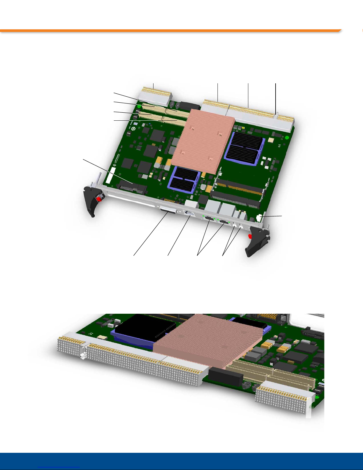
Chapter 5: Connectors
J1
P2
Hot-Swap
Ejector Switch
Connector (P3)
P1
J2J3J5
J11
J12
J13
J14
SATA
Hard Disk
Connector
(Optional)
USB
Connectors
(J10, J15)
Ethernet
Connectors
(J8 and J9)
RS-232
RJ-45
Console
Port (J7)
DVI-I
Connector
(J6)
CompactPCI Backplane Connectors
PTMC
Connectors
(Optional)
DDR SDRAM
Connectors
E
D
C
B
A
11
J1
1
15
25/1
J3
19
J2
J5
1
22
22/1
E
D
C
B
A
Figure 5-1: Connector Locations
Figure 5-2: Backplane Connectors Pin Locations
86
Page 87

Backplane Connectors
J1 (IPMB/Power Connector)
J1 is a 125-pin, 2 mm x 2 mm, female, 32-bit, CompactPCI-style connector providing rear-p anel
access to IPMB and power. Rows 12-14 are used for connector keying. See Table 5-2, “J1
CompactPCI Bus Connector Pinout,” for pin definitions and Figure 5-2, “Backplane
Connectors Pin Locations,” on page 86, for pin placement.
Table 5-2: J1 CompactPCI Bus Connector Pinout
Pin # Z A B C D E F
25
24 AD[1] 5V V(I/O) AD[0] ACK64#
23 3.3V AD[4] AD[3] 5V AD[2]
22 AD[7] GND 3.3V AD[6] AD[5]
21 3.3V AD[9] AD[8] M66EN C/BE[0]#
20 AD[12] GND V(I/O) AD[11] AD[10]
19 3.3V AD[15] AD[14] GND AD[13]
18 SERR# GND 3.3V PAR C/BE[1]#
17 3.3V IPMB_SCL IPMB_SDA GND PERR#
16 DEVSEL# GND V(I/O) STOP# LOCK#
15 3.3V FRAME# IRDY# PWRON# TRDY#
14
12
11 AD[18] AD[17] AD[16] GND C/BE[2]#
10 AD[21] GND 3.3V AD[20] AD[19]
9 C/BE[3]# RSV AD[23] GND AD[22]
8 AD[26] GND V(I/O) AD[25] AD[24]
7 AD[30] AD[29] AD[28] GND AD[27]
6 REQ# GND 3.3V FB_CLK AD[31]
5 BRSVP1A5 BRSVP1B5 PCI_RST# GND GNT0#
4 IPMB_PWR HAPPY# V(I/O) INTP INTS
3 INTA# INTB# INTC# 5V INTD#
2 TCK 5V TMS TDO TDI
1 5V -12V TRST# +12V 5V
5V REQ64# ENUM# 3.3V 5V
G
N
D
Backplane Connectors
G
KEY13
N
D
87
Page 88

Chapter 5: Connectors
J2 (V(I/O) Connector)
J2 is a 110-pin, 2 mm x 2 mm, right-angle, female, 64-bit, CompactPCI-style connector
providing rear-panel access to V(I/O) and ground. See Table 5-3, “J2 V(I/O) Connector Pinout,”
for pin definitions and Figure 5-2, “Backplane Connectors Pin Locations,” on page 86, for pin
placement
Table 5-3: J2 V(I/O) Connector Pinout
Pin #ZABCDEF
22
21 CLK6 GND RSV RSV PRTACH
20 CLK5 GND ALT_SYSEN# GND XOUT#
19 GND GND SMB_SDA SMB_SCL XIN#
18 BRSVP2A18 BRSVP2B18 BRSVP2C18 GND BRSVP2E18
17 BRSVP2A17 GND PRST# REQ6#/FTHSI GNT6#/FTHSO
16 BRSVP2A16 BRSVP2B16 DEG# GND BRSVP2E16
15 BRSVP2A15 GND FAL# REQ5# GNT5#
14 1V Pre Charged 1V Pre Charged 1V Pre Charged GND 1V Pre Charged
13 1V Pre Charged GND V(I/O) 1V Pre Charged 1V Pre Charged
12 1V Pre Charged 1V Pre Charged 1V Pre Charged GND 1V Pre Charged
1 1 1V Pre Charged GND V(I/O) 1V Pre Charged 1V Pre Charged
10 1V Pre Charged 1V Pre Charged 1V Pre Charged GND 1V Pre Charged
9 1V Pre Charged GND V(I/O) 1V Pre Charged 1V Pre Charged
8 1V Pre Charged 1V Pre Charged 1V Pre Charged GND 1V Pre Charged
7 1V Pre Charged GND V(I/O) 1V Pre Charged 1V Pre Charged
6 1V Pre Charged 1V Pre Charged 1V Pre Charged GND 1V Pre Charged
5 1V Pre Charged 64EN# V(I/O) 1V Pre Charged 1V Pre Charged
4 RSS# BRSVP2B4 1V Pre Charged GND 1V Pre Charged
3CLK4 GND GNT3#REQ4#GNT4#
2 CLK2 CLK3 SYSEN# GNT2# REQ3#
1 CLK1 GND REQ1# GNT1# REQ2#
GA4 GA3 GA2 GA1 GA0
G
N
D
G
N
D
88
Page 89

J3 (Rear-Panel Gigabit Ethernet Connector)
J3 is a 95-pin, 2 mm x 2 mm, female connector providing rear-panel access to Ethernet A and
Ethernet B. See Table 5-4, “J3 Rear-Panel Gigabit Ethernet Connector Pinout,” for pin
definitions and Figure 5-2, “Backplane Connectors Pin Locations,” on page 86, for pin
placement.
Table 5-4: J3 Rear-Panel Gigabit Ethernet Connector Pinout
Pin # Z A B C D E F
19
18 LPA_DA+ LPA_DA- GND LPA_DC+ LPA_DC17 LPA_DB+ LPA_DB- GND LPA_DD+ LPA_DD16 LPB_DA+ LPB_DA- GND LPB_DC+ LPB_DC15 LPB_DB+ LPB_DB- GND LPB_DD+ LPB_DD14 RESV RESV RESV RESV RESV
13 RESV RESV RESV RESV RESV
12 RESV RESV RESV RESV RESV
11 RESV RESV RESV RESV RESV
10 RESV RESV RESV RESV RESV
9 RESV RESV RESV RESV RESV
8 RESV RESV RESV RESV RESV
7 RESV RESV RESV RESV RESV
6 RESV RESV RESV RESV RESV
5 RESV RESV RESV RESV RESV
4 RESV RESV RESV RESV RESV
3 RESV RESV RESV RESV RESV
2 RESV RESV RESV RESV RESV
1 RESV RESV RESV RESV RESV
RESV RESV RESV RESV RESV
G
N
D
Backplane Connectors
G
N
D
89
Page 90

Chapter 5: Connectors
J5 (Rear-Panel User I/O Connector)
J5 is a 110-pin, 2 mm x 2 mm, female connector providing rear-panel access to the following:
• COM port • Video • Power and Ground • USB • SATA
•SMBus •Eject •RPIO Present •JTAG
See Table 5-5, “J5 Rear-Panel User I/O Connector Pinout,” for pin definitions and Figure 5-2,
“Backplane Connectors Pin Locations,” on page 86, for pin placement.
Table 5-5: J5 Rear-Panel User I/O Connector Pinout
Pin # A B C D E F
22 RESV RESV V5V USB2- USB2+
21 GND GND V5V GND GND
20 SATA_TX4_P SATA_TX4_N V5V RESV J5_SDA
19 SATA_RX4_P SATA_RX4_N V5V RESV J5_SCL
18 SATA_TX3_P SATA_TX3_N GND RESV RESV
17 SATA_RX3_P SATA_RX3_N GND RESV IPMB PWR
16 SATA_TX2_P SATA_TX2_N GND RESV RS232_TXD_CON
15 SATA_RX2_P SATA_RX2_N GND RESV RS232_RXD_CON
14 SATA_TX1_P SATA_TX1_N GND RESV RESV
13 SATA_RX1_P SATA_RX1_N GND RESV RESV
12 GND GND GND RESV RESV
11 RESV RESV RESV RESV RESV
10 RESV RESV DBG_RPIO_DET_L RESV RP_DDCCLK
9 RESV RESV RESV RESV RP_VSYNC
8 RESV RESV RESV RESV RP_BLUE_A
7 RESV RESV RESV RESV RP_HSYNC
6 RESV 5565_TDI RESV 5565_TRST_L RP_GRN_A
5 RESV 5565_TMS RESV 5565_TDO RP_DDCDAT
4 V3_3V V3_3V V3_3V V3_3V RP_RED_A
3 RESV RESV RESV RESV RESV
2 RESV RESV RESV RESV RESV
1 RESV 5565_TCK RPIO_PRSNT_L RP_BLUE_LED_L RP_EJECT_L
G
N
D
Front Panel Connectors
The following topics describe connectors on the front panel of the CPC5565:
• “DVI-I Connector (J6)” on page 91
• “RS-232 RJ-45 Console Port (J7)” on page 92
• “Ethernet Connectors (J8 and J9)” on page 92
• “USB Connectors (J10, J15)” on page 93
90
Page 91
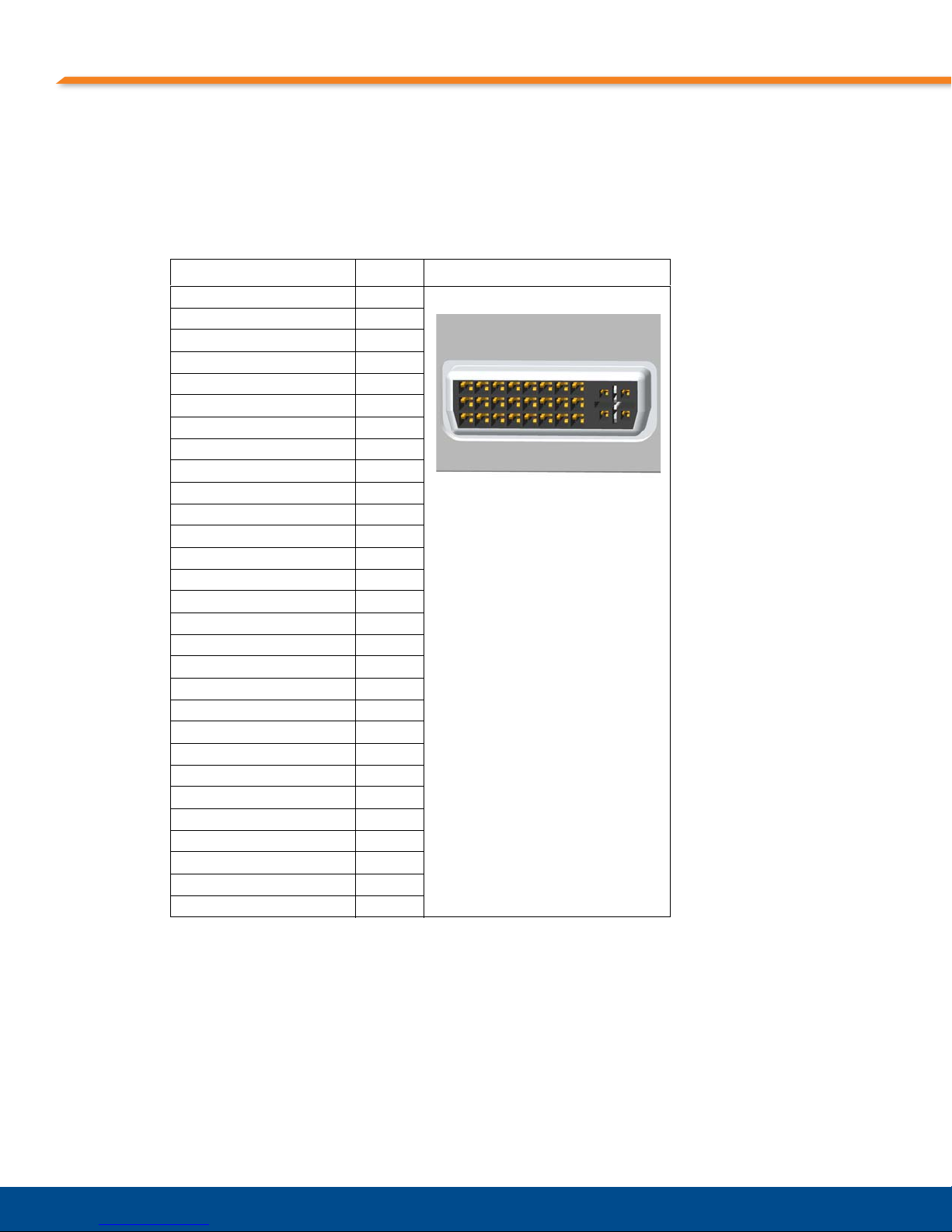
DVI-I Connector (J6)
1
C1 C2
C3 C4
2345678
9 10 111213141516
17 18 19 20 21 22 23 24
The CPC5565 includes a front-panel DVI-I video connector, which supports both digital video
signaling and analog signaling.
Table 5-6: DVI-I Connector J6 Pinout
Pin # Name Front View
TMDS_DATA2- 1
TMDS_DATA2+ 2
TMDS_DATA2/4SHIELD 3
TMDS_DATA4- 4
TMDS_DATA4+ 5
DDC_CLK_SCL 6
DDC_DATA_SDA 7
ANALOG_VERT_SYNC 8
TMDS_DATA1- 9
TMDS_DATA1+ 10
TMDS_DATA1/3SHIELD 11
TMDS_DATA3- 12
TMDS_DATA3+ 13
+5V 14
GND 15
HOT_PLUG_DETECT 16
TMDS_DATA0- 17
TMDS_DATA0+ 18
TMDS_DATA0/5SHIELD 19
TMDS_DATA5- 20
TMDS_DATA5+ 21
TMDS_CLK_SHIELD 22
TMDS_CLK+ 23
TMDS_CLK- 24
ANALOG_RED C1
ANALOG_GREEN C2
ANALOG_BLUE C3
ANALOG_HSYNC C4
ANALOG_GND C5
Front Panel Connectors
91
Page 92
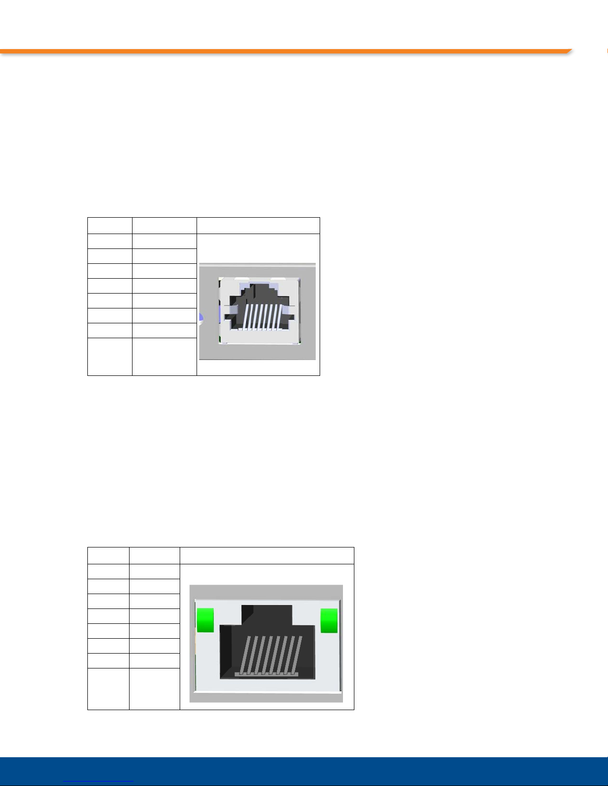
Chapter 5: Connectors
81
81
RS-232 RJ-45 Console Port (J7)
J7 is an 8-pin, RJ-45 connector providing the COM1 interface on the CPC5565's front panel.
This connector accepts RJ-45 male connectors on standard RJ-45 to DB9 cables (see “Serial
Cables” on page 99). RS-232 signal levels and 15KV ESD protection are provided by the
interface. COM1 interface signals are also directed out J5 (Rear-Panel User I/O Connector).
See Table 5-7, “RJ-45 Console Port J7 Pinout,” for pin definitions and Figure 5-1, “Connector
Locations,” on page 86, for connector identification.
Table 5-7: RJ-45 Console Port J7 Pinout
Pin # Name Front View
1RTS
2DTR
3TXD (OUT)
4GND
5GND
6RXD (IN)
7DSR
8CSR
Ethernet Connectors (J8 and J9)
Two RJ-45 connectors on the CPC5565's front panel provide two 1000 Mbps (1000Base-T)
Ethernet channels. Two bicolor LEDs are located inside each RJ-45 connector:
• Front panel ENET link
• Front panel ENET activity
See the topic “LED Indicators” on page 30, for more information. See Table 5-8, “Ethernet
Connectors J8 and J9 Pinout,” for pin definitions and Figure 5-1, “Connector Locations,” on
page 86, for connector identification.
Table 5-8: Ethernet Connectors J8 and J9 Pinout
Pin # Name Front View
1BI_DA+
2BI_DA3BI_DB+
4 BI_DC+
5 BI_DC6BI_DB7 BI_DD+
8 BI_DD-
92
Page 93

USB Connectors (J10, J15)
J10 and J15 are 4-pin, USB 2.0 Port 0 and Port 1 interface connectors on the CPC5565's front
panel. USB2 (Port 2) is directed out rear-panel I/O connector J5. See Table 5-9, “USB
Connectors J10, J15 Pinout,” for pin definitions and Figure 5-1, “Connector Locations,” on
page 86, for connector identification.
Table 5-9: USB Connectors J10, J15 Pinout
Pin # Function
1 +5V Fused
2 DATA3 DATA+
4 GND
Internal Connectors
The following topics describe connectors on the CPC5565 PCB:
Internal Connectors
• “PTMC Connectors (J11, J12, J13, and J14) (Optional)” on page 93
• “DDR2 SDRAM Connectors (P1, P2)” on page 98
• “Hot-Swap Ejector Switch Connector (P3)” on page 98
• “SATA Hard Disk Connector (Optional)” on page 98
PTMC Connectors (J11, J12, J13, and J14) (Optional)
The PTMC interface is implemented on the CPC5565 with connectors J11-J14. See the
following tables for PTMC connector pinouts.
• Table 5-10, “PTMC Connector J11 Pinout,” on page 94
• Table 5-11, “PTMC Connector Pin Map (J12),” on page 95
• Table 5-12, “PTMC Connector Pin Map (J13),” on page 96
• Table 5-13, “PTMC Connector Pin Map (J14),” on page 97
93
Page 94
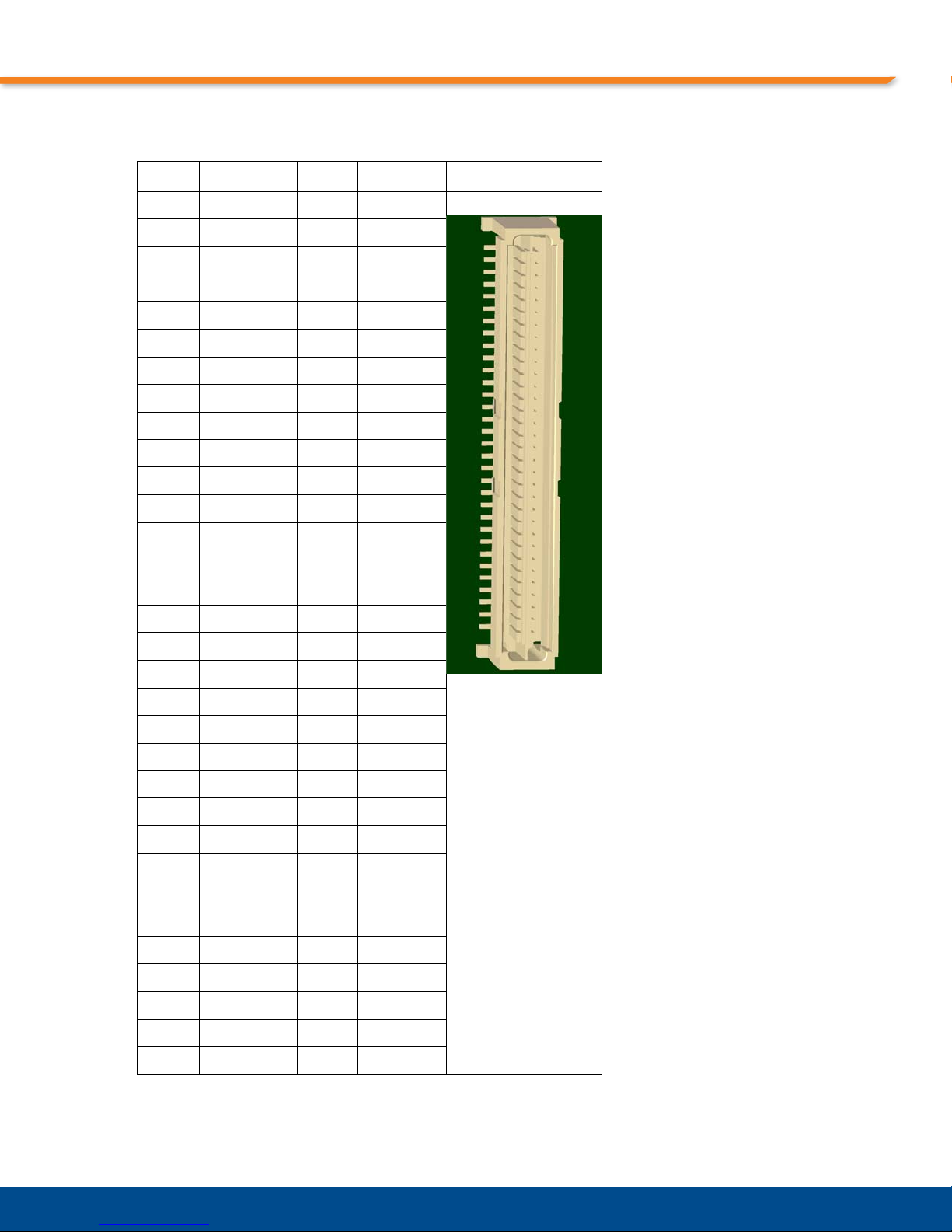
Chapter 5: Connectors
12
34
56
78
910
11 12
13 14
15 16
17 18
19 20
21 22
23 24
25 26
27 28
29 30
31 32
33 34
35 36
37 38
39 40
41 42
43 44
45 46
47 48
49 50
51 52
53 54
55 56
57 58
59 60
61 62
63 64
Table 5-10: PTMC Connector J11 Pinout
Pin # Net Pin # Net Socket View
1 TCK 2 -12V
3 GND 4 INTA_L
5 INTB_L 6 INTC_L
7 PRES_L 8 5V
9 INTD_L 10 N/C
11 GND 12 N/C
13 PCI_CLK 14 GND
15 GND 16 GNT_L
17 REQ_L 18 5V
19 3.3V (VIO) 20 AD31
21 AD28 22 AD27
23 AD25 24 GND
25 GND 26 CBE3
27 AD22 28 AD21
29 AD19 30 5V
31 3.3V (VIO) 32 AD17
33 FRAME_L 34 GND
35 GND 36 IRDY_L
37 DEVSEL_L 38 5V
39 PCIXCAP 40 PLOCK_L
41 SCL 42 SDA
43 PAR_L 44 GND
45 3.3V (VIO) 46 AD15
47 AD12 48 AD11
49 AD9 50 5V
51 GND 52 CBE0
53 AD6 54 AD5
55 AD4 56 GND
57 3.3V (VIO) 58 AD3
59 AD2 60 AD1
61 AD0 62 5V
63 GND 64 REQ64_L
94
Page 95

Table 5-11: PTMC Connector Pin Map (J12)
Pin # Net Pin # Net
1 +12V 2 N/C
3N/C 4N/C
5N/C 6GND
7GND 8N/C
9N/C 10N/C
11 BMODE2_L 12 3.3V
13 PCIRST_L 14 BMODE3_L
15 3.3V 16 BMODE4_L
17 REQ_L 18 GND
19 AD30 20 AD29
21 GND 22 AD26
Internal Connectors
23 AD24 24 GND
25 IDSEL 26 AD23
27 3.3V 28 AD20
29 AD18 30 GND
31 AD16 32 CBE2
33 GND 34 N/C
35 TRDY_L 36 IRDY_L
37 GND 38 STOP_L
39 PERR_L 40 GND
41 3.3V 42 SERR_L
43 CBE1_L 44 GND
45 AD14 46 AD13
47 GND 48 AD10
49 AD8 50 3.3V
51 AD7 52 N/C
53 3.3V 54 N/C
55 N/C 56 GND
57 N/C 58 N/C
59 GND 60 N/C
61 ACK64_L 62 3.3V
63 GND 64 N/C
95
Page 96

Chapter 5: Connectors
Table 5-12: PTMC Connector Pin Map (J13)
Pin # Net Pin # Net
1N/C 2 GND
3GND4 N/C
5 CBE6 6 GND
7 CBE4 8 GND
9 PTID2 10 N/C
11 AD63 12 3.3V
13 AD61 14 GND
15 GND 16 BMODE4_L
17 AD59 18 GND
19 AD57 20 GND
21 PTID0 22 AD26
23 AD55 24 GND
25 AD53 26 GND
27 GND 28 AD20
29 AD51 30 GND
31 AD49 32 GND
33 GND 34 N/C
35 AD47 36 I RDY_L
37 AD45 38 GND
39 PTENB_L 40 AD44
41 AD43 42 AD42
43 AD41 44 GND
45 GND 46 AD40
47 AD39 48 AD38
49 AD37 50 GND
51 GND 52 AD36
53 AD35 54 AD34
55 AD33 56 GND
57 PTID1 58 AD32
59 N/C 60 N/C
61 N/C 62 GND
63 GND 64 N/C
96
Page 97

Table 5-13: PTMC Connector Pin Map (J14)
Pin # Net Pin # Net
1 TP2A_P 2 TP2C_P
3 TP2A_N 4 TP2C_N
5GND6GND
7 TP2B_P 8 TP2D_P
9 TP2B_N 10 TP2D_N
11 GND 12 GND
13 TP3A_P 14 TP3C_P
15 TP3A_N 16 TP3C_N
17 GND 18 GND
19 TP3B_P 20 TP3D_P
21 TP3B_N 22 TP3D_N
Internal Connectors
23 GND 24 GND
25 N/C 26 N/C
27 N/C 28 N/C
29 N/C 30 N/C
31 N/C 32 N/C
33 N/C 34 N/C
35 N/C 36 N/C
37 N/C 38 N/C
39 N/C 40 N/C
41 N/C 42 N/C
43 N/C 44 N/C
45 N/C 46 N/C
47 N/C 48 N/C
49 N/C 50 N/C
51 N/C 52 N/C
53 N/C 54 N/C
55 N/C 56 N/C
57 N/C 58 N/C
59 N/C 60 N/C
61 N/C 62 N/C
63 N/C 64 N/C
97
Page 98

Chapter 5: Connectors
DDR2 SDRAM Connectors (P1, P2)
P1 and P2 are 90°, 200-pin connectors that accommodate 1.8V, 200-pin, PC2-3200 DDR2-400
SDRAM Registered SDRAM used for system memory. See Figure 5-1, “Connector Locations,”
on page 86, for connector identification. For more information about system memory, see the
topic “Memory Configuration” on page 34.
Hot-Swap Ejector Switch Connector (P3)
P3 is a 3-pin, vertical, 1.25 mm (.049 in), surface-mount connector linking the hot-swap switch
to the board's lower ejector mechanism. This switch is tied to logic on the CPC5565 to sense a
board extraction or insertion. See Table 5-14, “P3 Hot-Swap Ejector Switch Connector Pinout,”
for pin definitions and Figure 5-1, “Connector Locations,” on page 86, for connector
identification.
Table 5-14: P3 Hot-Swap Ejector Switch Connector Pinout
Pin # Function
1 Common
2 Latched
3 Unlatched
SATA Hard Disk Connector (Optional)
The Serial ATA hard disk connector implemented on the CPC5565 supports SATA drives but
does not support the SAS portion of the connector. One port is routed to the connector. See
Figure 5-1, “Connector Locations,” on page 86, for the connector location.
98
Page 99
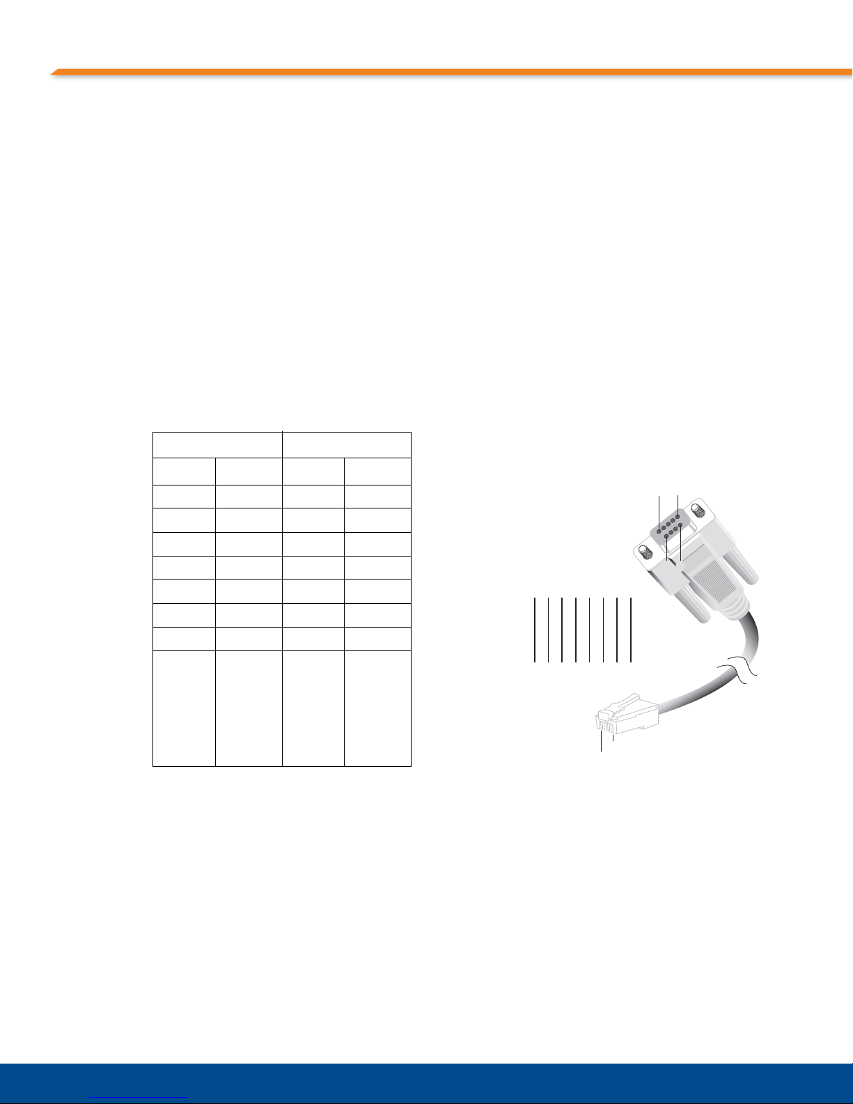
Cables
15
9
Female DB9
Connector Pin
Male RJ-45
Connector Pin
3
6
5
5
784
7
5423628
1
Pin 1
Pin 8
6
Serial Cables
The front panel connector RS-232 RJ-45 Console Port (J7) may be used to access the shelf
management software (see Chapter 4, “System Monitoring and Alarms”). Some shelf
managers require a DB-9 connector for this purpose. A male RJ-45 to female DB-9
management cable requires the following parts:
• Male RJ-45 connector
• High quality cable, such as Category 5
• Female DB-9 connector
The “Management Cable Pinout” table and figure show the required connections. This cable is
available from PT as part number ACC7340-120.
Table 5-15: Management Cable Pinout
RJ-45 DB9
Cables
Pin # Signal Pin # Signal
1 RTS 8 CTS
2 DSR 6 DTR
3 RxD 2 TxD
4 GND 5 GND
5 GND 5 GND
6 TxD 3 RxD
7 DTR 4 DSR
8 CTS 7 RTS
J5 (Rear-Panel User I/O Connector) may also be used to access the Command Line Interface.
If an RTM blade is attached to J5, such as the RTM4811, please refer to the RTM manual for
cabling information. See “User Documentation” on page 117 for links to PT product
documentation.
99
Page 100

Chapter 5: Connectors
100
 Loading...