

Page 1

USER
SP-7145/7147
15” / 17” Fanless Panel PC
Powered by Intel
®
Atom
®
E3845 /
Celeron
®
J1900 CPU Processor
With DVI-I, 3COM, 4USB & 2LAN
SP-7145/7147 M2
MANUAL
Page 2

SP-7145/7147
15”/17” High Performance Panel PC
COPYRIGHT NOTICE & TRADEMARK
All trademarks and registered trademarks mentioned herein are the
property of their respective owners.
This manual is copyrighted in August 2017. You may not reproduce or
transmit in any form or by any means, electronic, or mechanical,
including photocopying and recording.
DISCLAIMER
This user’s manual is meant to assist users in installing and setting up
the system. The information contained in this document is subject to
change without any notice.
CE NOTICE
This is a class A product. In a domestic environment this product may
cause radio interference in which case the user may be required to take
adequate measures.
Page 3
FCC NOTICE
CAUTION: Danger of explosion may occur when the battery
is incorrectly replaced. Replace the battery only with the
same or equivalent type recommended by the manufacturer.
Dispose of used batteries according to the manufacturer’s
instructions.
WARNING: Some internal parts of the system may have high
electrical voltage. We strongly recommend that only qualified
engineers are allowed to service and disassemble the
system. If any damages should occur on the system and are
caused by unauthorized servicing, it will not be covered by
the product warranty.
This equipment has been tested and found to comply with the limits for
a Class A digital device, pursuant to part 15 of the FCC Rules. These
limits are designed to provide reasonable protection against harmful
interference when the equipment is operated in a commercial
environment. This equipment generates, uses, and can radiate radio
frequency energy and, if not installed and used in accordance with the
instruction manual, may cause harmful interference to radio
communications. Operation of this equipment in a residential area is
likely to cause harmful interference in which case the user will be
required to correct the interference at his own expense.
You are cautioned that any change or modifications to the equipment
not expressly approve by the party responsible for compliance could
void your authority to operate such equipment.
Page 4

Contents
Revision History ............................................................................................ vii
1 Introduction ......................................................................................... 1-1
1.1 About This Manual .................................................................... 1-2
2 Getting Started .................................................................................... 2-1
2.1 Package List .............................................................................. 2-2
2.2 System Diagrams ...................................................................... 2-3
2.3 System Specifications ............................................................... 2-9
2.4 Safety Precautions .................................................................. 2-11
3 System Configuration ......................................................................... 3-1
3.1 External I/O Ports Diagrams ..................................................... 3-2
3.1.1 Rear I/O Ports Diagram (DC IN: 9 ~ 36V) ......................... 3-2
3.1.2 Rear I/O Ports Diagram (DC IN: 12V) ............................... 3-2
3.2 JUMPER & CONNECTOR QUICK REFERENCE TABLE ........ 3-2
3.3 COMPONENT LOCATIONS ..................................................... 3-3
3.3.1 Top View and Jumper Settings of SP-7145/7147 .............. 3-3
3.4 Setting Jumpers ........................................................................ 3-5
3.5 Setting Main Board Connectors and Jumpers .......................... 3-7
3.5.1 LVDS POWER SELECTION ............................................. 3-7
3.5.2 BACKLIGHT INVERTER PWM VOLTAGE SELECTION .. 3-8
3.5.3 POWER-ON MODE SELECTION ..................................... 3-9
3.5.4 BACKLIGHT ENABLE SELECTION ............................... 3-10
3.5.5 VGA/DVI SELECTION .................................................... 3-11
3.5.6 LVDS RESOLUTION SELECTION ................................. 3-12
i
Page 5

3.5.7 COM3 PIN9 DEFINITION SELECTION GUIDE .............. 3-13
3.5.8 COM4 VOLTAGE SELECTION ....................................... 3-14
3.5.9 AUDIO PORT .................................................................. 3-15
3.5.10 BATTERY WAFER .......................................................... 3-16
3.5.11 COM2 and COM3 PORTS .............................................. 3-16
3.5.12 COM4 CONNECTOR ...................................................... 3-17
3.5.13 COM5 CONNECTOR ...................................................... 3-18
3.5.14 COM6 CONNECTOR ...................................................... 3-18
3.5.15 DVI-I & COM PORT ......................................................... 3-19
3.5.16 FAN CONNECTOR ......................................................... 3-20
3.5.17 DC 12V CONNECTOR .................................................... 3-20
3.5.18 DIO WAFER (optional) .................................................... 3-21
3.5.19 FRONT CONNECTOR .................................................... 3-21
3.5.20 INVERTER WAFER......................................................... 3-22
3.5.21 KB/MS PORT .................................................................. 3-23
3.5.22 LAN & USB2.0 PORT ...................................................... 3-24
3.5.23 LAN& USB2.0/3.0 PORT ................................................. 3-25
3.5.24 SATA CONNECTOR ........................................................ 3-27
3.5.25 USB CONNECTOR ......................................................... 3-28
3.5.26 MINI PCIE CONNECTOR ............................................... 3-29
3.5.27 PCIE BUS ........................................................................ 3-30
3.5.28 LPC CONNECTOR ......................................................... 3-31
3.5.29 CLEAR CMOS DATA SELECTION ................................. 3-32
3.6 DAUGHTER BOARD BR-6062 JUMPER QUICK REFERENCE
TABLE ..................................................................................... 3-33
3.7 DAUGHTER BOARD BR-6062 COMPONENT LOCATIONS . 3-33
3.7.1 BR-6062 Top View ........................................................... 3-33
3.8 SETTING DAUGHTER BOARD BR-6062 JUMPERS ............ 3-34
ii
Page 6

3.8.1 RS-485 AUTO FLOW CONTROL FOR JCOM1_1 & JCOM1
......................................................................................... 3-34
3.8.2 RS-232/422/485 SELECTION FOR JCOM1_1 & JCOM1
......................................................................................... 3-35
3.8.3 RS-485 AUTO FLOW CONTROL FOR JCOM2_1 .......... 3-36
3.8.4 RS-232/422/485 SELECTION FOR JCOM2_1 ............... 3-37
3.9 DAUGHTER BOARD SR-6100 CONNECTOR & JUMPER
QUICK REFERENCE TABLE ................................................. 3-38
3.10 DAUGHTER BOARD SR-6100 COMPONENT LOCATIONS . 3-38
3.10.1 SR-6100 Top View ........................................................... 3-38
3.11 SETTING DAUGHTER BOARD SR-6100 CONNECTORS &
JUMPERS ............................................................................... 3-39
3.11.1 VIN Connector (+9V~+36V) ............................................ 3-39
3.11.2 VOUT Connector (+12V) ................................................. 3-39
3.11.3 RUN CONTROL INPUT SELECTION ............................. 3-40
3.11.4 PULSE SKIPPING MODE SELECTION ......................... 3-41
3.11.5 CONTINUOUS MODE SELECTION ............................... 3-41
4 Software Utilities ................................................................................. 4-1
4.1 Introduction ................................................................................ 4-2
4.2 Installing Intel® Chipset Software Installation Utility .................. 4-5
4.2.1 Introduction ........................................................................ 4-5
4.2.2 Intel® Chipset Software Installation Utility.......................... 4-5
4.3 Intel® Trusted Execution Engine Installation Utility ................... 4-6
4.4 Installing Graphics Driver Utility ................................................ 4-7
4.5 Installing LAN Driver Utility ........................................................ 4-8
4.6 Intel® USB 3.0 eXtensible Host Controller Utility ..................... 4-9
iii
Page 7

4.7 Installing Sound Driver Utility .................................................. 4-10
4.8 Installing Resistive Touch Driver Utility ................................... 4-10
4.9 Installing Projected Capacitive Touch Driver Utility ................. 4-11
5 BIOS SETUP ........................................................................................ 5-1
5.1 Introduction ................................................................................ 5-2
5.2 Accessing Setup Utility .............................................................. 5-3
5.3 Main ........................................................................................... 5-7
5.4 Advanced .................................................................................. 5-9
5.4.1 Advanced – Trusted Computing (BayTrail-I only)............ 5-10
5.4.2 Advanced – ACPI Settings .............................................. 5-11
5.4.3 Advanced – F81866 Super IO Configuration .................. 5-12
5.4.4 Advanced – Hardware Monitor ........................................ 5-19
5.4.5 Advanced – F81866 Watchdog Configuration ................. 5-21
5.4.6 Advanced – CPU Configuration ...................................... 5-22
5.4.7 Advanced – IDE Configuration ........................................ 5-25
5.4.8 OS Selection (BayTrail-D only) ........................................ 5-26
5.4.9 Advanced – CSM Configuration ...................................... 5-27
5.4.10 Advanced – USB Configuration ....................................... 5-29
5.5 Chipset .................................................................................... 5-31
5.5.1 Chipset – North Bridge .................................................... 5-32
5.5.2 Chipset – South Bridge.................................................... 5-36
5.6 Security ................................................................................... 5-42
5.7 Boot ......................................................................................... 5-44
5.8 Save & Exit .............................................................................. 5-47
iv
Page 8

Appendix A System Diagrams ....................................................... 1
SP-7145 System Exploded Diagram ................................................................. 2
SP-7145 Touch Panel & LCD Display Exploded Diagram ............................. 3
SP-7145 Touch Panel & LCD Display Exploded Diagram ............................. 5
SP-7145 Touch Panel & LCD Display Exploded Diagram ............................. 7
SP-7145 Touch Panel & LCD Display Exploded Diagram ............................. 9
SP-7145 Box PC Exploded Diagram ............................................................... 11
SP-7145 Box PC Exploded Diagram ............................................................... 13
SP-7145 Box PC Exploded Diagram ............................................................... 15
SP-7145 Box PC Exploded Diagram ............................................................... 17
SP-7145 HDD Tray Exploded Diagram ........................................................... 19
SP-7145 Panel Mount Exploded Diagram ...................................................... 20
SP-7147 System Exploded Diagram ............................................................... 21
SP-7147 Touch Panel & LCD Display Exploded Diagram ........................... 22
SP-7147 Touch Panel & LCD Display Exploded Diagram ........................... 24
SP-7147 Box PC Exploded Diagram ............................................................... 26
SP-7147 Box PC Exploded Diagram ............................................................... 28
SP-7147 Box PC Exploded Diagram ............................................................... 30
SP-7147 Box PC Exploded Diagram ............................................................... 32
SP-7147 HDD Tray Exploded Diagram ........................................................... 34
SP-7147 Panel Mount Exploded Diagram ...................................................... 35
Appendix B Technical Summary ................................................... 1
System Block Diagram ........................................................................................ 2
Interrupt Map ......................................................................................................... 3
I/O MAP ................................................................................................................. 7
Memory Map ....................................................................................................... 11
Configuring WatchDog Timer ............................................................................ 13
Flash BIOS Update ............................................................................................ 16
v
Page 9

List of Figures
Figure 3-1. Main Board Component Location (Top View) ................. 3-3
Figure 3-2. Daughter Board BR-6062 Component Location (Top View)
.................................................................................. 3-33
Figure 3-2. Daughter Board SR-6100 Component Location (Top View)
.................................................................................. 3-38
Figure 5-1. Extensible Firmware Interface Diagram ......................... 5-2
Figure 5-2. POST Screen with AMI Logo.......................................... 5-4
vi
Page 10

Revision History
Version No.
Revision History
Date
M1
Initial Release
2017/06/27
M2
1. SP-7145/7147 system diagrams have been
changed.
2. SP-7145/7147 rear I/O ports diagrams
have been changed.
3. SP-7145/7147 exploded diagrams have
been changed.
2017/08/15
The revision history of SP-7145/7147 User Manual is described below:
vii
Page 11

SP-7145/7147 SERIES USER MANUAL
Page: 1-1
1 Introduction
This chapter provides the introduction for the SP-7145/7147
system as well as the framework of the user manual.
The following topic is included:
• About This Manual
Page 12

Chapter 1 Introduction
SP-7145/7147 SERIES USER MANUAL
Page: 1-2
1.1 About This Manual
Thank you for purchasing our SP-7145/7147 system. The SP-7145/7147 is an updated
system designed to be comparable with the highest performance of IBM AT personal
computers. The SP-7145/7147 provides faster processing speed, greater expandability
and can handle more tasks than before. This manual is designed to assist you how to
install and set up the whole system. It contains 5 chapters and 2 appendixes. Users can
configure the system according to their own needs. This user manual is intended for
service personnel with strong hardware background. It is not intended for general
users.
The following section outlines the structure of this user manual.
Chapter 1 Introduction
This chapter introduces you to the background of this manual.
Chapter 2 Getting Started
This chapter describes the package contents and outlines the system specifications. It
also includes the physical illustrations for the SP-7145/7147 system. Read the safety
reminders carefully on how to take care of your system properly.
Chapter 3 System Configuration
This chapter outlines the locations of the motherboard and daughter boards
components and their respective functions. You will learn how to set the jumpers and
configure the system to meet your own needs.
Chapter 4 Software Utilities
This chapter contains helpful information for proper installations of the Intel Chipset
Software Installation Utility, Intel Trusted Execution Engine Driver Utility, Graphics
Driver Utility, LAN Driver Utility, Intel USB3.0 eXtensible Host Controller Utility,
Sound Driver Utility, Resistive Touch Driver Utility and Projected Capacitive Touch
Driver Utility.
Chapter 5 AMI BIOS Setup
This chapter indicates you how to change the BIOS configurations.
Appendix A System Assembly Diagrams
This appendix provides the system exploded diagrams and part numbers of
SP-7145/7147.
Appendix B Technical Summary
This appendix provides the information about the system block diagram, allocation
maps for system resources, Watchdog Timer Configuration and Flash BIOS Update.
Page 13

SP-7145/7147 SERIES USER MANUAL
Page: 2-1
2 Getting Started
This chapter provides the information for the SP-7145/7147
system. It describes how to set up the system quickly and
outlines the system specifications.
The following topics are included:
• Package List
• System Overview
• System Diagrams
• System Specification
• Safety Precautions
Experienced users can go to Chapter 3 System
Configuration on page 3-1 for a quick start.
Page 14
Chapter 2 Getting Started
SP-7145/7147 SERIES USER MANUAL
Page: 2-2
Item
Q’ty
SP-7145/7147
1
Manual / Driver DVD
1
Quick Guide
1
AC Power Cord
1
Power Adapter
1
Power Adapter Cable
1
2.1 Package List
If you discover any of the items listed below are damaged or lost, please
contact your local distributor immediately.
Page 15
SP-7145/7147 SERIES USER MANUAL
Page: 2-3
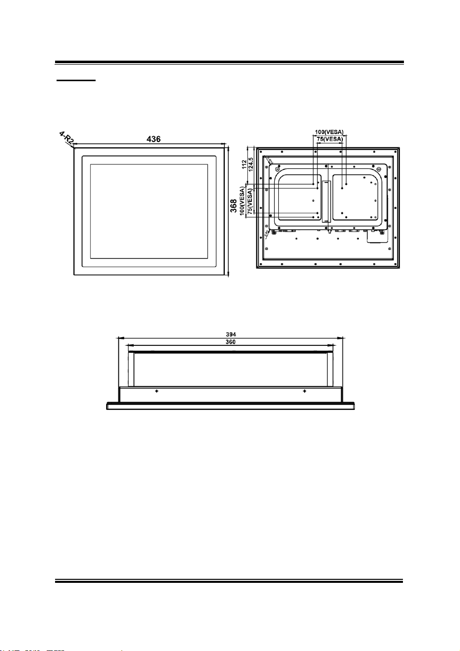
2.2 System Diagrams
Front View
Rear View
Top View
SP-7145
Chapter 2 Getting Started
Unit: mm
Page 16
SP-7145/7147 SERIES USER MANUAL
Page: 2-4
Bottom View
DC-IN: 9 ~ 36V
DC-IN: 12V
Unit: mm
Left Side View
Right Side View
Chapter 2 Getting Started
Page 17

SP-7145/7147 SERIES USER MANUAL
Page: 2-5
Quarter View
Chapter 2 Getting Started
Page 18
SP-7145/7147 SERIES USER MANUAL
Page: 2-6
SP-7147
Front View
Rear View
Top View
Chapter 2 Getting Started
Unit: mm
Page 19
SP-7145/7147 SERIES USER MANUAL
Page: 2-7
Bottom View
DC-IN: 9 ~ 36V
DC-IN: 12V
Left Side View
Right Side View
Chapter 2 Getting Started
Unit: mm
Page 20
SP-7145/7147 SERIES USER MANUAL
Page: 2-8
Quarter View
Chapter 2 Getting Started
Page 21
SP-7145/7147 SERIES USER MANUAL
Page: 2-9
2.3 System Specifications
System
CPU Support
Intel
®
E3845 (Bay Trail-I)/J1900 (Bay Trail-D)
Memory Support
2 x 204-pin DDR3L 1333/1600MHz SO-DIMM
(up to 8GB)
OS Support
Win 7, Win 10, Microsoft Azure,
Linux Ubuntu 14.04
Drive Bay
2 x 2.5” SATAII HDD or SSD
Power Supply
DC-in 9V~36V
Power Adapter
12V, 60W / 24V, 120W
Expansion Slot
1 x half-sized Mini PCIe slot
Mounting Support
Wall mount / VESA 75 / VESA 100 / Panel mount
Net Weight &
Dimension (WxHxD)
SP-7145: 6.8 kg, 408mm x 320mm x 26mm
SP-7147: 7.9 kg, 436mm x 368mm x 27.4mm
Certificate
CE/FCC
I/O Ports
Serial Port
COM1/2/3/4 for RS-232 (COM4 optional)
COM3/4 pin9 5V/12V/RI selectable
COM5/6 for RS-232/422/485 via daughter board
(optional)
COM4/5/6 are not available for optional DC IN 12V
SKU
USB
3 x USB 2.0, 1 x USB 3.0
Display Port
1 x DVI-I
LAN
2 x LAN, RJ-45 (Controller: 2 x Intel I210-IT),
Wake-On-LAN
Audio
1 x Line-out, 1 x Line-in,1 x Mic-in
Digital I/O
4in/4out (optional) (not available for optional DC IN
12V SKU)
Keyboard / Mouse
2 x PS/2 ports
DC-IN
1 x 3-pin terminal block connector on rear I/O
Power On/Off
1 x Power On/Off button and 1 x Remote Switch on rear
I/O
Display
LCD Panel Size
SP-7145: 15” TFT LCD(LED) XGA
(resolution: 1024 x 768)
Chapter 2 Getting Started
Page 22

Chapter 2 Getting Started
SP-7145/7147 SERIES USER MANUAL
Page: 2-10
SP-7147: 17” TFT LCD(LED) SXGA
(resolution: 1280 x 1024)
Touchscreen
Projected resistive / capacitive touch screen
Environment
Operating Temp.
(with airflow)
HDD: 0°C ~ 40°C (32°F ~ 104°F)
SSD: 0°C ~ 45°C (32°F ~ 113°F)
Wide Temperature:
0°C ~50°C SSD (with J1900, Sunlight readable panel)
0°C ~55°C SSD (with J1900)
-20°C ~50°C SSD (with E3845, Sunlight readable panel)
-20°C ~55°C SSD (with E3845)
Storage Temp.
-20°C ~ 80°C (-4°F ~ 176°F)
Humidity
20%~ 90%
Page 23

Chapter 2 Getting Started
SP-7145/7147 SERIES USER MANUAL
Page: 2-11
2.4 Safety Precautions
Before operating this system, read the following information carefully to protect your
systems from damages, and extend the life cycle of the system.
1. Check the Line Voltage
• The operating voltage for the power supply should be within the range of
100V to 240V AC; otherwise the system may be damaged.
2. Environmental Conditions
• Place your SP-7145/7147 on a sturdy, level surface. Be sure to allow
enough space around the system to have easy access needs.
• Avoid installing your SP-7145/7147 system in extremely hot or cold places.
• Avoid direct sunlight exposure for a long period of time (for example, in a
closed car in summer time. Also avoid the system from any heating device.).
Or do not use SP-7145/7147 when it has been left outdoors in a cold winter
day.
• Avoid moving the system rapidly from a hot place to a cold place, and vice
versa, because condensation may occur inside the system.
• Protect your SP-7145/7147 from strong vibrations which may cause hard
disk failure.
• Do not place the system too close to any radio-active device. Radio-active
device may cause signal interference.
• Always shut down the operating system before turning off the power.
3. Handling
• Avoid placing heavy objects on the top of the system.
• Do not turn the system upside down. This may cause the hard drive to
malfunction.
• Do not allow any objects to fall into this device.
• If water or other liquid spills into the device, unplug the power cord
immediately.
4. Good Care
• When the outside case gets stained, remove the stains using neutral washing
agent with a dry cloth.
• Never use strong agents such as benzene and thinner to clean the surface of
the case.
• If heavy stains are present, moisten a cloth with diluted neutral washing
agent or alcohol and then wipe thoroughly with a dry cloth.
• If dust is accumulated on the case surface, remove it by using a special
vacuum cleaner for computers.
Page 24

SP-7145/7147 SERIES USER MANUAL
Page: 3-1
3 System Configuration
This chapter contains helpful information about the
external I/O Ports diagram, and jumper & connector
settings, and component locations for the main board and
daughter board.
The following topics are included:
• External I/O Ports Diagram
• Main Board Jumper Settings and Component
Locations
• How to Set Jumpers
• Setting Main Board Connectors and Jumpers
• Daughter Board Component Locations
• Setting Daughter Board Connectors and Jumpers
Page 25
Chapter 3 Hardware Configuration
SP-7145/7147 SERIES USER MANUAL
Page: 3-2
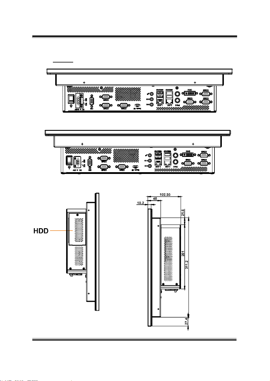
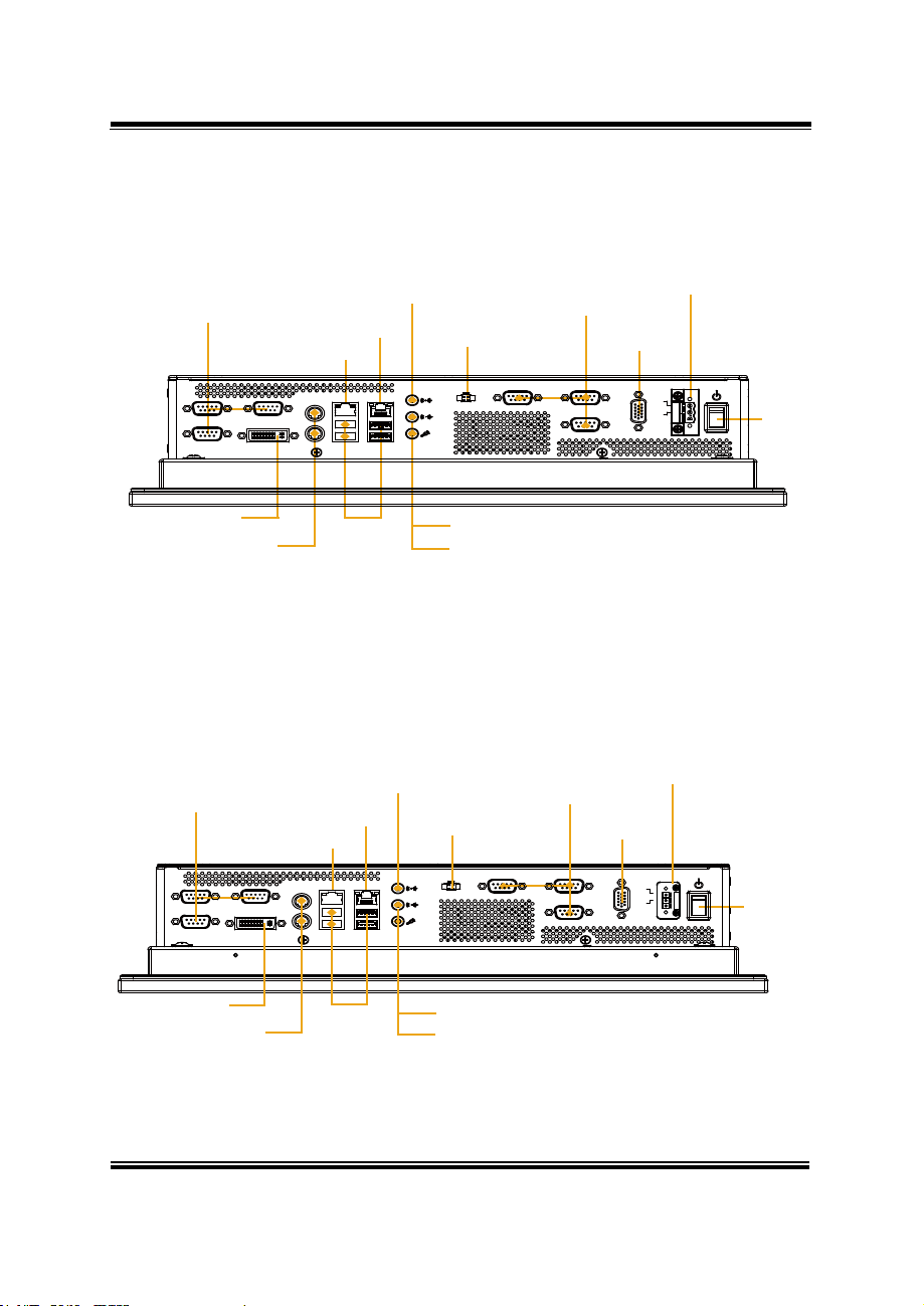
3.1 External I/O Ports Diagrams
3.1.1 Rear I/O Ports Diagram (DC IN: 9 ~ 36V)
COM
COM
Connector
COM2
COM3
COM1
DVI-I
PS/2
LAN1
LAN1
USB2.0/2.0
LAN2
LAN2
USB2.0/3.0
Line-in
Remote
Switch
Remote SW
Connector
(optional)
(optional)
COM4 COM5
COM6
DC IN 9~36V
DIO
DC IN 9~36V
DIO
VCC
GND
Power
Button
DVI-I
PS/2 Mouse/
USB
Connector
Line-out
Mic-in
Keyboard
Connector
3.1.2 Rear I/O Ports Diagram (DC IN: 12V)
COM
COM
Connector
COM2
COM3
DVI-I
PS/2 Mouse/
Keyboard
Connector
COM1
DVI-I
LAN1
LAN1
PS/2
USB2.0/2.0
USB
Connector
LAN2
LAN2
USB2.0/3.0
Line-in
Remote
Switch
Remote SW
Line-out
Mic-in
Connector
(optional)
COM4 COM5
COM6
DC IN 12V
DIO
(optional)
DIO
VCC
GND
DC IN 12V
Power
Button
Page 26

SP-7145/7147 SERIES USER MANUAL
Page: 3-2
JUMPER/CONNECTOR
NAME
LVDS Power Selection
JP4
Backlight Power Selection
JP5
AT/ATX Mode Selection
JP7
Backlight Enable Selection
JP9
VGA/DVI Selection
JP10
LVDS Resolution Selection
JP14, JP15
COM3 Voltage Selection
JP_COM3
COM4 Voltage Selection
JP_COM4
Audio Port
JAUDIO1
Battery Wafer
JBAT1
COM Port
JCOM2_3
COM4 Connector
JCOM4
COM5 Connector
JCOM5
COM6 Connector
JCOM6
DVI-I & COM Port
JCOM_DVII1
FAN Connector
JCPU_FAN1, JSYS_FAN1
DC 12V Connector
JDC_PWR1
DIO Wafer
JDIO1
Front Connector
JFP1
Inverter Wafer
JINV1
KB/MS Port
JKB_MS1
LAN & USB2.0 Port
JLAN_USB1
LAN& USB2.0/3.0 Port
JLAN_USB2
LVDS Connector
JLVDS1
SATA Connector
JSATA1, JSATA2
SATA Power Connector
JSATA_PWR1, JSATA_PWR2
USB Connector
JUSB1
MINI PCIE Connector
M_PCI_E1
PCIE BUS
PCI_E1
LPC Connector
JLPC1
Clear CMOS Data Selection
JP1
3.2 JUMPER & CONNECTOR QUICK REFERENCE TABLE
Chapter 3 Hardware Configuration
Page 27
SP-7145/7147 SERIES USER MANUAL
Page: 3-3
WARNING: Always disconnect the power cord when you are
working with connectors and jumpers on the main board.
Make sure both the system and peripheral devices are turned
OFF as sudden surge of power could damage sensitive
components. Make sure SP-7145/7147 is properly grounded.
Chapter 3 Hardware Configuration
3.3 COMPONENT LOCATIONS
3.3.1 Top View and Jumper Settings of SP-7145/7147
Figure 3-1. Main Board Component Location (Top View)
Page 28
SP-7145/7147 SERIES USER MANUAL
Page: 3-4
CAUTION: Observe precautions while handling electrostatic
sensitive components. Make sure to ground yourself to
prevent static charge while you are working on the
connectors and jumpers. Use a grounding wrist strap and
place all electronic components in any static-shielded
devices.
CAUTION: Always touch the motherboard components by
the edges. Never touch components such as a processor by
its pins. Take special cares while you are holding electronic
circuit boards by the edges only. Do not touch the mainboard
components.
Chapter 3 Hardware Configuration
Page 29
SP-7145/7147 SERIES USER MANUAL
Page: 3-5
Chapter 3 Hardware Configuration
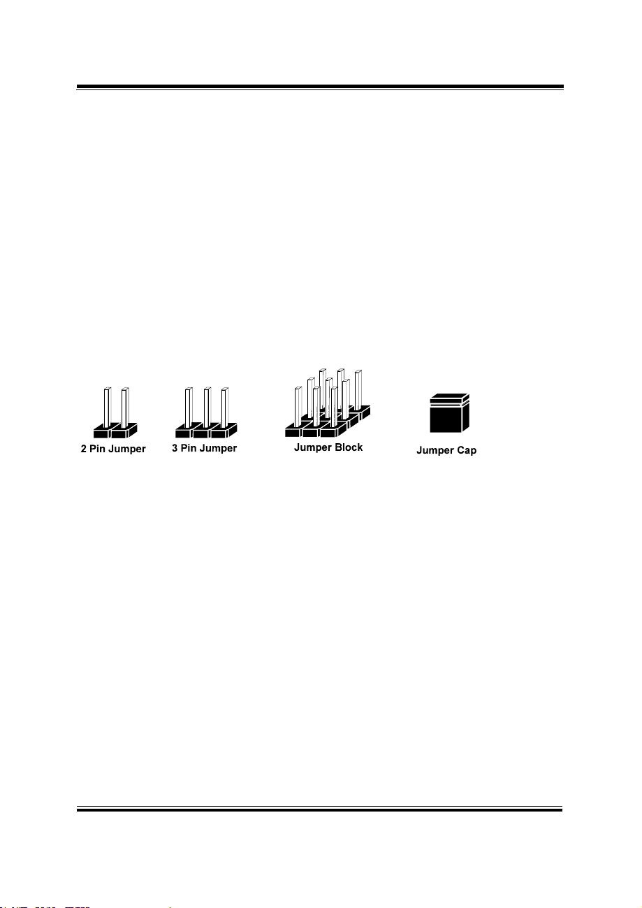
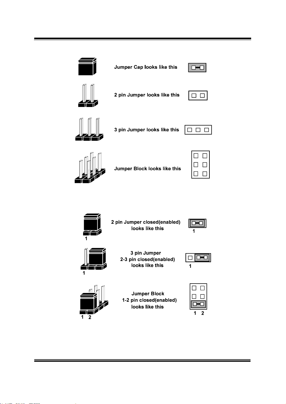
3.4 Setting Jumpers
You can configure your board by setting the jumpers. A jumper consists of two or
three metal pins with a plastic base mounted on the card. By using a small plastic
"cap", also known as the jumper cap (with a metal contact inside), you are able to
connect the pins. So you can configure your hardware settings by "opening" or
"closing" jumpers.
Jumpers can be combined into sets that are called jumper blocks. When jumpers are
all in the block, you have to put them together to set up the hardware configuration.
The figure below shows what this looks like.
Jumpers & Caps
If a jumper has three pins, for example, labeled 1, 2 and 3. You can connect pins 1 and
2 to create one setting and shorting. You can also select to connect pins 2 and 3 to
create another setting. The format of the jumper picture will be illustrated throughout
this manual. The figure below shows different types of jumpers and jumper settings.
Page 30
SP-7145/7147 SERIES USER MANUAL
Page: 3-6
Jumper diagrams
Jumper settings
Chapter 3 Hardware Configuration
Page 31

Chapter 3 Hardware Configuration
SP-7145/7147 SERIES USER MANUAL
Page: 3-7
SELECTION
JUMPTER SETTING
JUMPER ILLUSTRATION
3.3V
1-2
3 1
JP4
5V
2-3
3 1
JP4
3.5 Setting Main Board Connectors and Jumpers
3.5.1 LVDS POWER SELECTION
JP4: LVDS Power Selection
Note: Manufacturing default for SP-7145 is 3.3V.
Manufacturing default for SP-7147 is 5V.
Page 32

Chapter 3 Hardware Configuration
SP-7145/7147 SERIES USER MANUAL
Page: 3-8
SELECTION
JUMPTER SETTING
JUMPER ILLUSTRATION
3.3V
1-2
3
1
JP5
5V
2-3
3
1
JP5
GND
NC
3
1
JP5
3.5.2 BACKLIGHT INVERTER PWM VOLTAGE SELECTION
JP5: Backlight Inverter PWM Voltage Selection
Note: Manufacturing default for SP-7145 is 3.3V.
Manufacturing default for SP-7147 is 5V.
Page 33

Chapter 3 Hardware Configuration
SP-7145/7147 SERIES USER MANUAL
Page: 3-9
SELECTION
JUMPTER SETTING
JUMPER ILLUSTRATION
Auto-on
1-2
1
JP7
Select by BIOS
NC
1
JP7
3.5.3 POWER-ON MODE SELECTION
JP7: Power-On Mode Selection
Note 1: Manufacturing default is Auto-on.
Note 2: Manufacturing default for BS-H292 (SBOX) is "NC".
Note 3: Auto-On means that system will turn on automatically whenever the main
power is restored.
Page 34

SP-7145/7147 SERIES USER MANUAL
Page: 3-10
SELECTION
JUMPTER SETTING
JUMPER ILLUSTRATION
5V
2-3
1
3
JP9
3.3V
1-2
1
3
JP9
Chapter 3 Hardware Configuration
3.5.4 BACKLIGHT ENABLE SELECTION
JP9: BACKLIGHT ENABLE Selection
Note: Manufacturing default for SP-7145 is 3.3V.
Manufacturing default for SP-7147 is 5V.
Page 35

SP-7145/7147 SERIES USER MANUAL
Page: 3-11
SELECTION
JUMPTER SETTING
JUMPER ILLUSTRATION
DVI
(1-3)
(5-6)
5
6
1
2
JP10
VGA
(1-2)
(4-6)
5
6
1
2
JP10
3.5.5 VGA/DVI SELECTION
JP10: VGA/DVI Selection
Note: Manufacturing default is DVI.
Chapter 3 Hardware Configuration
Page 36

SP-7145/7147 SERIES USER MANUAL
Page: 3-12
SELECTION
JUMPTER SETTING
JUMPER ILLUSTRATION
1024x768
1CH/24bit
(for SP-7145)
JP15(4-6)
JP15(3-5)
JP14(2-4)
JP14(3-5)
5
6
1
2
JP14
5
6
1
2
JP15
1280x1024
2CH/24bit
(for SP-7147)
JP15(4-6)
JP15(1-3)
JP14(2-4)
JP14(3-5)
5
6
1
2
JP14
5
6
1
2
JP15
Chapter 3 Hardware Configuration
3.5.6 LVDS RESOLUTION SELECTION
JP14 & JP15: LVDS Resolution Selection
Page 37

SP-7145/7147 SERIES USER MANUAL
Page: 3-13
SELECTION
JUMPTER SETTING
JUMPER ILLUSTRATION
RI
1-2
5
6
1
2
JP_COM3
12V
3-4
5
6
1
2
JP_COM3
5V
5-6
5
6
1
2
JP_COM3
Chapter 3 Hardware Configuration
3.5.7 COM3 PIN9 DEFINITION SELECTION GUIDE
JP_COM3: COM3 Port pin9 RI/5V/12V Selection
Note: Manufacturing default is RI.
Page 38

SP-7145/7147 SERIES USER MANUAL
Page: 3-14
SELECTION
JUMPTER SETTING
JUMPER ILLUSTRATION
RI
1-2
21
65
JP_COM4
12V
3-4
21
65
JP_COM4
5V
5-6
21
65
JP_COM4
Chapter 3 Hardware Configuration
3.5.8 COM4 VOLTAGE SELECTION
JP_COM4: COM4 Voltage Selection
Note 1: Manufacturing default is RI.
Note 2: Manufacturing default for BS-H292 (SBOX)) is 5V (5-6).
Page 39

SP-7145/7147 SERIES USER MANUAL
Page: 3-15
PIN
ASSIGNMENT
32
LINE-IN-L
33
NC
34
NC
35
LINE-IN-R
PIN
ASSIGNMENT
22
LINE-OUT-L
23
NC
24
NC
25
LINE-OUT-R
PIN
ASSIGNMENT
1
GND
2
MIC_L
3
NC 4 NC
5
MIC_R
PIN
ASSIGNMENT
42
NC
43
NC
44
NC
1 2345
22232425
32333435
424344
JAUDIO1
3.5.9 AUDIO PORT
JAUDIO1: Line-In, Line-Out & Microphone
The connector can also support only Microphone.
Line-In:
Line-Out:
Mic-In:
Chapter 3 Hardware Configuration
Others:
Page 40

SP-7145/7147 SERIES USER MANUAL
Page: 3-16
PIN
ASSIGNMENT
1
RTC_BAT
2
GND
PIN
ASSIGNMENT
1
DCD
2
RXD
3
TXD
4
DTR
5
GND
6
DSR
7
RTS
8
CTS 9 RI
JCOM2_3
JBAT1
3.5.10 BATTERY WAFER
JBAT1: Battery Wafer
3.5.11 COM2 and COM3 PORTS
JCOM2_3: COM Port
Chapter 3 Hardware Configuration
Page 41

SP-7145/7147 SERIES USER MANUAL
Page: 3-17
3.5.12 COM4 CONNECTOR
PIN
ASSIGNMENT
PIN
ASSIGNMENT
1
DCD
6
DSR
2
RXD
7
RTS
3
TXD
8
CTS
4
DTR 9 RI 5 GND
10
NC
JCOM4
JCOM4: COM4 Connector
Chapter 3 Hardware Configuration
Page 42

SP-7145/7147 SERIES USER MANUAL
Page: 3-18
PIN
ASSIGNMENT
PIN
ASSIGNMENT
1
DCD
6
DSR
2
RXD
7
RTS
3
TXD
8
CTS
4
DTR 9 RI 5 GND
10
NC
PIN
ASSIGNMENT
PIN
ASSIGNMENT
1
DCD
6
DSR
2
RXD
7
RTS
3
TXD
8
CTS
4
DTR 9 RI 5 GND
10
NC
JCOM6
JCOM5
3.5.13 COM5 CONNECTOR
JCOM5: COM5 Connector
3.5.14 COM6 CONNECTOR
JCOM6: COM6 Connector
Chapter 3 Hardware Configuration
Page 43

SP-7145/7147 SERIES USER MANUAL
Page: 3-19
PIN
ASSIGNMENT
PIN
ASSIGNMENT
1
TMDS_D2-
2
TMDS_D2+
3
GND
4
NC 5 NC
6
DDC_CLK
7
DDC_DATA
8
VSYNC
9
TMDS_D1-
10
TMDS_D1+
11
GND
12
NC
13
NC
14
5V
15
GND
16
HPD
17
TMDS_D0-
18
TMDS_D0+
19
GND
20
NC
21
NC
22
GND
23
TMDS_CLK+
24
TMDS_CLK-
C1
RED
C2
GREEN
C3
BLUE
C4
HSYNC
C5
CND - -
PIN
ASSIGNMENT
1
DCD
2
RXD
3
TXD
4
DTR
5
GND
6
DSR
7
RTS
8
CTS 9 RI
JCOM_DVII1
3.5.15 DVI-I & COM PORT
JCOM_DVII1: DVI-I & COM PORT
DVI-I: DVI Connector
COM1: COM Connector
Chapter 3 Hardware Configuration
Page 44

SP-7145/7147 SERIES USER MANUAL
Page: 3-20
PIN
ASSIGNMENT
1
GND
2
12V
3
FAN_CONTROL
4
FAN_SIGNAL
PIN
ASSIGNMENT
1
12V 2 12V
3
GND
4
GND
JDC_PWR1
JCPU_FAN1/
JSYS_FAN1
3.5.16 FAN CONNECTOR
JCPU_FAN1, JSYS_FAN1: Fan Connector
3.5.17 DC 12V CONNECTOR
JDC_PWR1: DC 12V Connector
Chapter 3 Hardware Configuration
Page 45

SP-7145/7147 SERIES USER MANUAL
Page: 3-21
PIN
ASSIGNMENT
PIN
ASSIGNMENT
1
5V
6
GND
2
DIN0
7
DOUT0
3
DIN1
8
DOUT1
4
DIN2
9
DOUT2
5
DIN3
10
DOUT3
PIN
ASSIGNMENT
PIN
ASSIGNMENT
1
HDD_LED+
7
RESET SWITCH
2
PWR_LED+
8
SPEAKER SIGNAL
3
HDD_LED-
9
POWER BUTTON
4
PWR_LED-
10
SPEAKER SIGNAL
5
GND
11
GND
6
SPK_VCC
12
SPEAKER SIGNAL
JFP1
JDIO1
3.5.18 DIO WAFER (optional)
JDIO1: DIO Wafer
3.5.19 FRONT CONNECTOR
JFP1: Front Connector
Chapter 3 Hardware Configuration
Page 46

SP-7145/7147 SERIES USER MANUAL
Page: 3-22
PIN
ASSIGNMENT
1
12V 2 12V
3
GND
4
PWM SIGNAL
5
GND
6
BACKLIGHT EN
JINV1
3.5.20 INVERTER WAFER
JINV1: Inverter Wafer
Chapter 3 Hardware Configuration
Page 47

SP-7145/7147 SERIES USER MANUAL
Page: 3-23
PIN
ASSIGNMENT
1
DATA
2
NC
3
GND 4 5V 5 CLK 6 NC
PIN
ASSIGNMENT
7
DATA
8
NC
9
GND
10
5V
11
CLK
12
NC
3
12
4
56
9
78
10
1112
MS
KB
JKB_MS1
3.5.21 KB/MS PORT
JKB_MS1: KB/MS Port
Keyboard:
Mouse:
Chapter 3 Hardware Configuration
Page 48

SP-7145/7147 SERIES USER MANUAL
Page: 3-24
PIN
ASSIGNMENT
1
TX_D1+
2
TX_D1-
3
RX_D2+
4
BI_D3+
5
BI_D3-
6
RX_D2-
7
BI_D4+
8
BI_D4-
Yellow Orange/
Green
JLAN_USB1
USB2.0:
PIN
ASSIGNMENT
1
5V 2 D-
3
D+ 4 GND
3.5.22 LAN & USB2.0 PORT
JLAN_USB1: LAN & USB2.0 PORT
LAN:
Chapter 3 Hardware Configuration
Page 49

SP-7145/7147 SERIES USER MANUAL
Page: 3-25
3.5.23 LAN& USB2.0/3.0 PORT
PIN
ASSIGNMENT
1
TX_D1+
2
TX_D1-
3
RX_D2+
4
BI_D3+
5
BI_D3-
6
RX_D2-
7
BI_D4+
8
BI_D4-
PIN
ASSIGNMENT
B1
VBUS
B2
D-
B3
D+
B4
GND
B5
STDA_SSRX-
B6
STDA_SSRX+
B7
GND
B8
STDA_SSTX-
B9
STDA_SSTX+
Yellow Orange/
Green
B1 B4
B9 B5
JLAN_USB2
JLAN_USB2: LAN & USB2.0/3.0 PORT
LAN:
USB2.0:
Chapter 3 Hardware Configuration
Page 50

SP-7145/7147 SERIES USER MANUAL
Page: 3-26
2-28. LVDS CONNECTOR
PIN
ASSIGNMENT
PIN
ASSIGNMENT
1
LVDS_VCC
2
GND
3
LVDS1_CLK-
4
LVDS1_CLK+
5
GND
6
LVDS1_D2-
7
LVDS1_D2+
8
GND
9
LVDS1_D1-
10
LVDS1_D1+
11
LVDS1_D3+
12
LVDS1_D3-
13
LVDS1_D0+
14
LVDS1_D0-
15
GND
16
LVDS0_CLK+
17
LVDS0_CLK-
18
GND
19
LVDS0_D2+
20
LVDS0_D2-
21
GND
22
LVDS0_D1+
23
LVDS0_D1-
24
GND
25
LVDS0_D0+
26
LVDS0_D0-
27
LVDS0_D3+
28
LVDS0_D3-
29
LVDS_VCC
30
LVDS_VCC
2
1 29
30
JLVDS1
JLVDS1: LVDS Connector
Chapter 3 Hardware Configuration
Page 51

Chapter 3 Hardware Configuration
SP-7145/7147 SERIES USER MANUAL
Page: 3-27
PIN
ASSIGNMENT
1
GND
2
TX+
3
TX-
4
GND
5
RX-
6
RX+
7
GND
PIN
ASSIGNMENT
1
5V 2 GND
3
GND
4
12V
71
JSATA1/
JSATA2
1 4
JSATA_PWR1/
JSATA_PWR2
3.5.24 SATA CONNECTOR
JSATA1, JSATA2: Two Serial ATA Connectors
2-30. SATA POWER CONNECTOR
JSATA_PWR1, JSATA_PWR2: SATA Power Connector
Page 52

SP-7145/7147 SERIES USER MANUAL
Page: 3-28
PIN
ASSIGNMENT
PIN
ASSIGNMENT
1
5V 2 5V 3 D- 4 D- 5 D+ 6 D+ 7 GND
8
GND
9
GND
10
GND
JUSB1
3.5.25 USB CONNECTOR
JUSB1: USB Connector
Chapter 3 Hardware Configuration
Page 53

SP-7145/7147 SERIES USER MANUAL
Page: 3-29
PIN
ASSIGNMENT
PIN
ASSIGNMENT
1
WAKE#
2
3.3V
3
NC 4 GND
5
NC 6 1.5V
7
CLKREQ#
8
NC 9 GND
10
NC
11
REFCLK-
12
NC
13
REFCLK+
14
NC
15
GND
16
NC
17
NC
18
GND
19
NC
20
NC
21
GND
22
PERST#
23
PERn0
24
3.3V
25
PERp0
26
GND
27
GND
28
1.5V
29
GND
30
SMB_CLK
31
PETn0
32
SMB_DATA
33
PETp0
34
GND
35
GND
36
USB_D-
37
GND
38
USB_D+
39
3.3V
40
GND
41
3.3V
42
NC
43
GND
44
NC
45
NC
46
NC
47
NC
48
1.5V
49
NC
50
GND
51
NC
52
3.3V
M_PCI_E1
3.5.26 MINI PCIE CONNECTOR
M_PCI_E1: MINI PCIE Connector
Chapter 3 Hardware Configuration
Page 54

SP-7145/7147 SERIES USER MANUAL
Page: 3-30
PIN
ASSIGNMENT
PIN
ASSIGNMENT
A1
NC
B1
12V
A2
12V
B2
12V
A3
12V
B3
12V
A4
GND
B4
GND
A5
NC
B5
SMB_CLK
A6
NC
B6
SMB_DATA
A7
NC
B7
GND
A8
NC
B8
3.3V
A9
3.3V
B9
NC
A10
3.3V
B10
3.3V_SB
A11
PWRGD
B11
WAKE#
A12
GND
B12
NC
A13
REFCLK+
B13
GND
A14
REFCLK-
B14
HSOP0
A15
GND
B15
HSON0
A16
HSIP0
B16
GND
A17
HSIN0
B17
PRSNT#
A18
GND
B18
GND
PCI_E1
3.5.27 PCIE BUS
PCI_E1: PCIE BUS
Chapter 3 Hardware Configuration
Page 55

SP-7145/7147 SERIES USER MANUAL
Page: 3-31
PIN
ASSIGNMENT
PIN
ASSIGNMENT
1
CLK
2
GND
3
FRAME
4
NC 5 RESET
6
VCC5
7
LAD3
8
LAD2
9
VCC3
10
LAD1
11
LAD0
12
GND
13
SMBCLK
14
SMBDATA
15
3VSB
16
SERIRQ
17
GND
18
CLK RUN
19
SUS_TAT
20
DREQ0
1
20
2
19
JLPC1
3.5.28 LPC CONNECTOR
JLPC1: LPC Connector
Chapter 3 Hardware Configuration
Page 56

SP-7145/7147 SERIES USER MANUAL
Page: 3-32
SELECTION
JUMPER SETTINGS
JUMPER ILLUSTRATION
Normal
Open
(Default Setting)
JP1
Clear CMOS
Data
Close
JP1
Chapter 3 Hardware Configuration
3.5.29 CLEAR CMOS DATA SELECTION
Jumper Location: JP1
Description: Clear CMOS Data Selection
Step 1. Remove the main power of the PC.
Step 2. Close JP1 (pins 1-2) for 6 seconds by a cap.
Step 3. Remove the cap which is just used on JP1 (1-2), so that JP1 returns to
“OPEN”.
Step 4. Power on the PC and the PC will then auto-reboot for once in order to set
SoC’s register.
Step 5. Done!
Note: Please make sure the main power is off before you clear CMOS.
Page 57

SP-7145/7147 SERIES USER MANUAL
Page: 3-33
JUMPER
NAME
JP1
RS-485 Auto Flow Control for JCOM1_1 & JCOM1
JP2
RS-232/422/485 Selection for JCOM1_1 & JCOM1
JP3
RS-485 Auto Flow Control for JCOM2_1
JP3
RS-232/422/485 Selection for JCOM2_1
Chapter 3 Hardware Configuration
3.6 DAUGHTER BOARD BR-6062 JUMPER QUICK REFERENCE
TABLE
DAUGHTER BOARD BR-6062: 50 x 89mm Daughter Board with 2UART to
RS-232/422/485 Transceiver
3.7 DAUGHTER BOARD BR-6062 COMPONENT LOCATIONS
3.7.1 BR-6062 Top View
Figure 3-2. Daughter Board BR-6062 Component Location (Top View)
Page 58

SP-7145/7147 SERIES USER MANUAL
Page: 3-34
SELECTION
JUMPTER
SETTING
JUMPER ILLUSTRATION
Normal
(Default)
1-2
3 1
JP1
Auto
2-3
3 1
JP1
Chapter 3 Hardware Configuration
3.8 SETTING DAUGHTER BOARD BR-6062 JUMPERS
3.8.1 RS-485 AUTO FLOW CONTROL FOR JCOM1_1 & JCOM1
JP1: RS-485 Auto Flow Control Selection for JCOM1_1 and JCOM1
Page 59

SP-7145/7147 SERIES USER MANUAL
Page: 3-35
Selection
Jumper Setting
Jumper Illustration
RS-232
(Default)
Open
JP2
RS-422
1-2, 3-4, 9-10
JP2
RS-485
1-2, 5-6, 7-8
JP2
Chapter 3 Hardware Configuration
3.8.2 RS-232/422/485 SELECTION FOR JCOM1_1 & JCOM1
JP2: RS-232/422/485 Selection for JCOM1_1 & JCOM1
Page 60

SP-7145/7147 SERIES USER MANUAL
Page: 3-36
SELECTION
JUMPTER
SETTING
JUMPER ILLUSTRATION
Normal
(Default)
1-2
3 1
JP3
Auto
2-3
3 1
JP3
Chapter 3 Hardware Configuration
3.8.3 RS-485 AUTO FLOW CONTROL FOR JCOM2_1
JP3: RS-485 Auto Flow Control Selection for JCOM2_1
Page 61

SP-7145/7147 SERIES USER MANUAL
Page: 3-37
Selection
Jumper Setting
Jumper Illustration
RS-232
(Default)
Open
JP4
RS-422
1-2, 3-4, 9-10
JP4
RS-485
1-2, 5-6, 7-8
JP4
Chapter 3 Hardware Configuration
3.8.4 RS-232/422/485 SELECTION FOR JCOM2_1
JP4: RS-232/422/485 Selection for JCOM2_1
Page 62

SP-7145/7147 SERIES USER MANUAL
Page: 3-38
JUMPER
NAME
JP1
Run Control Output Selection
JP2/JP3
Pulse Skipping Mode Selection
JP2/JP3
Continuous Mode Selection
CONNECTOR
NAME
VIN
VIN Voltage Selection (+9V ~ +36V)
VOUT
VOUT Voltage Selection (+12V)
Chapter 3 Hardware Configuration
3.9 DAUGHTER BOARD SR-6100 CONNECTOR & JUMPER QUICK
REFERENCE TABLE
DAUGHTER BOARD SR-6100: 50 x 89mm Daughter Board with 2UART to
RS-232/422/485 Transceiver
3.10 DAUGHTER BOARD SR-6100 COMPONENT LOCATIONS
3.10.1 SR-6100 Top View
Figure 3-3. Daughter Board SR-6100 Component Location (Top View)
Page 63

SP-7145/7147 SERIES USER MANUAL
Page: 3-39
PIN
ASSIGNMENT
1
VIN+
2
VIN+
3
GND
4
GND
PIN
ASSIGNMENT
1
GND
2
GND
3
VOUT
4
VOUT
VIN
VOUT
Chapter 3 Hardware Configuration
3.11 SETTING DAUGHTER BOARD SR-6100 CONNECTORS &
JUMPERS
3.11.1 VIN Connector (+9V~+36V)
VIN: VIN Connector
3.11.2 VOUT Connector (+12V)
VIN: VIN Connector
Page 64

SP-7145/7147 SERIES USER MANUAL
Page: 3-40
SELECTION
JUMPTER
SETTING
JUMPER ILLUSTRATION
VIN+
(Turn On)
(Default)
1-2
JP1
GND
(Shut Down)
2-3
JP1
Chapter 3 Hardware Configuration
3.11.3 RUN CONTROL INPUT SELECTION
JP1: Run Control Input Selection
Page 65

Chapter 3 Hardware Configuration
SP-7145/7147 SERIES USER MANUAL
Page: 3-41
SELECTION
JUMPTER
SETTING
JUMPER ILLUSTRATION
Pulse
Skipping
Mode
(Default)
1-2
JP2
NC
Open
JP3
SELECTION
JUMPTER
SETTING
JUMPER ILLUSTRATION
NC
Open
JP2
Continuous
Mode
(Default)
1-2
JP3
3.11.4 PULSE SKIPPING MODE SELECTION
JP2/JP3: Pulse Skipping Mode Selection
3.11.5 CONTINUOUS MODE SELECTION
JP2/JP3: Continuous Mode Selection
Page 66

SP-7145/7147 SERIES USER MANUAL
Page: 4-1
4 Software Utilities
This chapter provides the detailed information that guides
users to install driver utilities for the system. The following
topics are included:
• Installing Intel® Chipset Software Installation Utility
• Installing Intel® Trusted Execution Engine Interface
• Installing Graphics Driver Utility
• Installing LAN Driver Utility
• Installing Intel® USB 3.0 eXtensible Host Controller
Utility
• Installing Sound Driver Utility
• Installing Resistive Touch Driver Utility
• Installing Projected Capacitive Touch Driver Utility
Page 67

Chapter 4 Software Utilities
SP-7145/7147 SERIES USER MANUAL
Page: 4-2
Filename (Assume that
DVD- ROM drive is D:)
Purpose
OS
DOS
Win7/32 bit
D:\Driver\Flash BIOS
For Aptio(EFI) BIOS update
utility
X
D:\Driver\Platform\Main Chip
Intel(R) Chipset Device
Software Installation Utility
X
D:\Driver\Platform\TXE
For Intel Trusted Execution
Engine Interface
X
D:\Driver\Platform\Graphics
Intel HD Graphics
X
D:\Driver\Platform\LAN Chip
Intel I210-IT For LAN Driver
installation
X
D:\Driver\ Platform\
USB3.0
Intel(R) USB 3.0 eXtensible
Host Controller Utility
X
D:\Driver\Platform\Sound
Codec
Realtek ALC888S For
Sound driver installation
X
D:\Driver\Platform\
Windows 7 KMDF
Windows Kernel-Mode
Driver Framework driver
installation
X
D:\Driver\Device\touch driver
Resistive touch driver
installation
X
D:\Driver\Device\touch
driver\WES7
Projected Capacitive touch
driver installation
X
For WES7 only
Filename (Assume that
DVD- ROM drive is D:)
Purpose
OS
DOS
Win7/64 bit
D:\Driver\Flash BIOS
For Aptio (EFI) BIOS
update utility
X
D:\Driver\Platform\Main Chip
Intel(R) Chipset Device
Software Installation Utility
X
D:\Driver\Platform\TXE
For Intel Trusted Execution
Engine Interface
X
4.1 Introduction
Enclosed with the SP-7145/7147 Series package is our driver utilities
contained in a DVD-ROM disk. Refer to the following tables for
driver locations:
X : Not support
: Support
Note: Install the driver utilities immediately after the OS installation is completed.
Page 68

Chapter 4 Software Utilities
SP-7145/7147 SERIES USER MANUAL
Page: 4-3
Filename (Assume that
DVD- ROM drive is D:)
Purpose
OS
DOS
Win7/64 bit
D:\Driver\Platform\Graphics
Intel HD Graphics
X
D:\Driver\Platform\LAN Chip
Intel I210-IT For LAN Driver
installation
X
D:\Driver\ Platform\
USB3
Intel(R) USB 3.0 eXtensible
Host Controller Utility
X
D:\Driver\Platform\Sound
Codec
Realtek ALC888S For
Sound driver installation
X
D:\Driver\Platform\
Windows 7 KMDF
Windows Kernel-Mode
Driver Framework driver
installation
X
D:\Driver\Device\touch driver
Resistive touch driver
installation
X
D:\Driver\Device\touch
driver\WES7
Projected Capacitive touch
driver installation
X
For WES7 only
Filename (Assume that
DVD- ROM drive is D:)
Purpose
OS
DOS
Win10/32 bit
D:\Driver\Flash BIOS
For Aptio(EFI) BIOS update
utility
X
D:\Driver\Platform\Main Chip
Intel(R) Chipset Device
Software Installation Utility
X
D:\Driver\Platform\TXE
For Intel Trusted Execution
Engine Interface
X
D:\Driver\Platform\Graphics
Intel HD Graphics
X
D:\Driver\Platform\LAN Chip
Intel I210-IT For LAN Driver
installation
X
D:\Driver\Platform\Sound
Codec
Realtek ALC888S For
Sound driver installation
X
D:\Driver\Device\touch driver
Resistive touch driver
installation
X
X : Not support
: Support
Note: Install the driver utilities immediately after the OS installation is completed.
X : Not support
: Support
Note: Install the driver utilities immediately after the OS installation is completed.
Page 69

Chapter 4 Software Utilities
SP-7145/7147 SERIES USER MANUAL
Page: 4-4
Filename (Assume that
DVD- ROM drive is D:)
Purpose
OS
DOS
Win10/64 bit
D:\Driver\Flash BIOS
For Aptio (EFI) BIOS
update utility
X
D:\Driver\Platform\Main Chip
Intel(R) Chipset Device
Software Installation Utility
X
D:\Driver\Platform\TXE
For Intel Trusted Execution
Engine Interface
X
D:\Driver\Platform\Graphics
Intel HD Graphics
X
D:\Driver\Platform\LAN Chip
Intel I210-IT For LAN Driver
installation
X
D:\Driver\Platform\Sound
Codec
Realtek ALC888S For
Sound driver installation
X
D:\Driver\Device\touch driver
Resistive touch driver
installation
X
X : Not support
: Support
Note: Install the driver utilities immediately after the OS installation is completed.
Page 70

Chapter 4 Software Utilities
SP-7145/7147 SERIES USER MANUAL
Page: 4-5
4.2 Installing Intel® Chipset Software Installation Utility
4.2.1 Introduction
The Intel® Chipset Software Installation Utility installs the Windows
*.INF files to the target system. These files outline to the operating
system how to configure the Intel chipset components in order to
ensure that the following functions work properly:
• Core PCI and ISAPNP Services
• PCIe Support
• SATA Storage Support
• USB Support
• Identification of Intel
4.2.2 Intel® Chipset Software Installation Utility
®
Chipset Components in the Device Manager
The utility pack is to be installed only for Windows® 7/10 series, and
it should be installed immediately after the OS installation is finished.
Please follow the steps below:
1 Connect the USB DVD-ROM device to SP-7145/7147 and insert
the driver disk.
2 Enter the Main Chip folder where the Chipset driver is located.
3 Select Windows 7 (32/64-bit) / Windows 10 (32/64-bit) for your
OS platform.
4 Click the chipset driver installation file for driver installation.
5 Follow the on-screen instructions to install the driver.
6 Once the installation is completed, shut down the system and
restart SP-7145/7147 for the changes to take effects.
Page 71

Chapter 4 Software Utilities
SP-7145/7147 SERIES USER MANUAL
Page: 4-6
4.3 Intel® Trusted Execution Engine Installation Utility
For Windows 7 only. Pre-install Microsoft's Kernel-Mode Driver
Framework (KMDF) version 1.11 before you install the Intel® Trusted
Execution Engine Installation Utility (TXE) in order to avoid errors in
Device Manager.
Installation Instructions for Kernel-Mode Driver Framework
(KMDF)
To install the Kernel-Mode Driver Framework (KMDF), follow the
steps below:
1 Insert the driver disk into a DVD-ROM device.
2 (For Windows 7 only) Enter the KMDF folder where the
installation driver file is located.
3 (For Windows 7 only) Click the Setup kmdf-1.11.exe file for
driver installation.
Installation Instructions for Intel® Trusted Execution Engine
Installation Utility
1 Connect the USB DVD-ROM device to SP-7145/7147 and insert
the driver disk.
2 Enter the TXE folder where the driver is located.
3 Select Windows 7 (32/64-bit) / Windows 10 (32/64-bit) for your
OS platform.
4 Click SetupTXE.exe file for TXE driver installation.
5 Follow the on-screen instructions to complete the installation.
Page 72

SP-7145/7147 SERIES USER MANUAL
Page: 4-7
Chapter 4 Software Utilities
6 Once the installation is completed, shut down the system and
restart SP-7145/7147 for the changes to take effect.
4.4 Installing Graphics Driver Utility
The graphics interface embedded in SP-7145/7147 can support a
wide range of display types. You can have dual displays via DVI-D
ports and make the system work simultaneously.
To install the Graphics driver utility, follow the steps below:
1 Connect the USB DVD-ROM device to SP-7145/7147 and insert
the driver disk.
2 Enter the Graphics folder where the driver is located.
3 Select Windows 7 (32/64-bit) / Windows 10 (32/64-bit) for your
OS platform.
4 Click the graphics driver installation file for driver installation.
5 Follow the on-screen instructions to complete the installation.
6 Once the installation is completed, shut down the system and
restart SP-7145/7147 for the changes to take effect.
Page 73

SP-7145/7147 SERIES USER MANUAL
Page: 4-8
Chapter 4 Software Utilities
4.5 Installing LAN Driver Utility
Enhanced with LAN function, SP-7145/7147 supports various network
adapters. To install the LAN Driver, follow the steps below:
1 Connect the USB DVD-ROM device to SP-7145/7147 and insert
the driver disk.
2 Enter the LAN folder where the driver is located.
3 Select Windows 7 (32/64-bit) / Windows 10 (32/64-bit) for your
OS platform.
4 Click the LAN driver installation file for driver installation.
5 Follow the on-screen instructions to complete the installation.
6 Once the installation is completed, shut down the system and
restart SP-7145/7147 for the changes to take effects.
For more details on the installation procedure, refer to the
README.txt file that you can find on LAN Driver Utility.
Page 74

SP-7145/7147 SERIES USER MANUAL
Page: 4-9
Chapter 4 Software Utilities
4.6 Intel® USB 3.0 eXtensible Host Controller Utility
(For Windows 7 Only) Intel® USB 3.0 eXtensible Host Controller
Driver supports the following Intel® Chipsets/Processors:
• Intel
• Intel
• Intel
• Intel
• Intel
®
8 Series/C220 series Chipset Family
® 4th
Generation Core
®
C610 series Chipset Family
®
9 Series Chipset Family
®
Pentium® Processor or Intel® Celeron® Processor N- & J-
TM
Processors
Series
• Intel
• Intel
• Intel
• Intel
®
5th generation Intel® CoreTM Processors
®
CoreTM M Processor
®
6th generation Intel® CoreTM processors
®
100 Series Chipset Family
To install the utility, follow the steps below:
1 Insert the driver disk into a DVD-ROM device.
2 Under Windows system, go to the directory where the driver is
located.
3 Run the application with administrative privileges.
Page 75

SP-7145/7147 SERIES USER MANUAL
Page: 4-10
Chapter 4 Software Utilities
4.7 Installing Sound Driver Utility
The sound function enhanced in this system is fully compatible with
Windows® 7/10 series.
To install the Sound Driver, follow the steps below:
1 Connect the USB DVD-ROM device to SP-7145/7147 and insert
the driver disk.
2 Open the Sound folder where the driver is located.
3 Select Windows 7 (32/64-bit) / Windows 10 (32/64-bit) for your
OS platform.
4 Click the Sound driver installation file for driver installation.
5 Follow the on-screen instructions to complete the installation.
6 Once the installation is completed, shut down the system and
restart SP-7145/7147 for the changes to take effect.
4.8 Installing Resistive Touch Driver Utility
To install the Resistive Touch Driver, follow the steps below:
1 Connect the USB DVD-ROM device to SP-7145/7147 and insert
the driver disk.
2 Enter the Touch driver folder where the driver is located.
3 Select Windows 7 (32/64-bit) / Windows 10 (32/64-bit) for your
OS platform.
4 Click the Touch driver installation file for driver installation.
5 Follow the on-screen instructions to complete the installation.
6 Once the installation is completed, shut down the system and
restart SP-7145/7147 for the changes to take effects.
Page 76

SP-7145/7147 SERIES USER MANUAL
Page: 4-11
Chapter 4 Software Utilities
4.9 Installing Projected Capacitive Touch Driver Utility
To install the Projected Capacitive Touch Driver, follow the steps
below:
1 Connect the USB DVD-ROM device to SP-7145/7147 and insert
the driver disk.
2 Enter the Touch driver > WES7 folder where the driver is
located.
3 Select WES 7 (32/64-bit) for your OS platform.
4 Click the Touch driver installation file for driver installation.
5 Follow the on-screen instructions to complete the installation.
6 Once the installation is completed, shut down the system and
restart SP-7145/7147 for the changes to take effects.
Page 77

SP-7145/7147 SERIES USER MANUAL
Page: 5-1
This chapter guides users how to configure the basic
system configurations via the BIOS (Basic Input / Output
System) Setup Utilities. The information of the system
configuration is saved in battery-backed CMOS RAM
and BIOS NVRAM so that the Setup information is
retained when the system is powered off. The BIOS
Setup Utilities consist of the following menu items:
• Accessing Setup Utilities
• Main Menu
• Advanced Menu
• Chipset Menu
• Security Menu
• Boot Menu
• Save & Exit Menu
5 BIOS SETUP
Page 78

SP-7145/7147 SERIES USER MANUAL
Page: 5-2
Chapter 5 BIOS Setup
5.1 Introduction
The SP-7145/7147 System uses an AMI (American Megatrends
Incorporated) Aptio BIOS that is stored in the Serial Peripheral Interface
Flash Memory (SPI Flash) and can be updated. The SPI Flash contains
the built-in BIOS setup program, Power-On Self-Test (POST), PCI
auto-configuration utility, LAN EEPROM information, and Plug and
Play support.
Aptio is AMI’s BIOS firmware based on the UEFI (Unified Extensible
Firmware Interface) specifications and the Intel Platform Innovation
Framework for EFI. The UEFI specification defines an interface
between the operating system and platform firmware. The interface
consists of data tables that contain platform-related information, boot
service calls, and runtime service calls that are available to the
operating system and its loader. These elements have combined to
provide a standard environment for booting the operating system and
running pre-boot applications.
The diagram below shows the Extensible Firmware Interface’s location
in the software stack.
Figure 5-1. Extensible Firmware Interface Diagram
Page 79

Chapter 5 BIOS Setup
SP-7145/7147 SERIES USER MANUAL
Page: 5-3
EFI BIOS provides an user interface that allows you to modify
hardware configuration, e.g. change the system date and time,
enable/disable a system component, determine bootable device priority,
set up personal password, etc., which is convenient for engineers to
perform modifications and customize the computer system and allows
technicians to troubleshoot the occurred errors when the hardware is
faulty.
The BIOS setup menu allows users to view and modify the BIOS
settings for the computer. After the system is powered on, users can
access the BIOS setup menu by pressing <Del> or <Esc> immediately
while the POST message is running before the operating system is
loading.
All the menu settings are described in details in this chapter.
5.2 Accessing Setup Utility
After the system is powered on, BIOS will enter the Power-On
Self-Test (POST) routines and the POST message will be displayed:
Page 80

Chapter 5 BIOS Setup
SP-7145/7147 SERIES USER MANUAL
Page: 5-4
Figure 5-2. POST Screen with AMI Logo
Press <Del> or <Esc> to access the Setup Utility program and the
Main menu of the Aptio Setup Utility will appear on the screen as
below:
Page 81

SP-7145/7147 SERIES USER MANUAL
Page: 5-5
Chapter 5 BIOS Setup
BIOS Setup Menu Initialization Screen
You may move the cursor by <↑> and <↓> keys to highlight the
individual menu items. As you highlight each item, a brief description
of the highlighted selection will appear on the right side of the screen.
The language of the BIOS setup menu interface and help messages are
shown in US English. You may use <↑> or <↓> key to select among the
items and press <Enter> to confirm and enter the sub-menu. The
following table provides the list of the navigation keys that you can use
while operating the BIOS setup menu.
Page 82

SP-7145/7147 SERIES USER MANUAL
Page: 5-6
BIOS Setup
Navigation Key
Description
<←> and <→>
Select a different menu screen (move the
cursor from the selected menu to the left or
right).
<↑> and <↓>
Select a different item (move the cursor from
the selected item upwards or downwards)
<Enter>
Execute the command or select the sub-menu.
<F2>
Load the previous configuration values.
<F3>
Load the default configuration values.
<F4>
Save the current values and exit the BIOS
setup menu.
<Esc>
Close the sub-menu.
Trigger the confirmation to exit BIOS setup
menu.
BIOS Message
Explanation
A first boot or
NVRAM reset
condition has been
detected.
BIOS has been updated or the battery was
replaced.
The CMOS defaults
were loaded.
Default values have been loaded after the
BIOS was updated or the battery was
replaced.
The CMOS battery
is bad or has been
recently replaced.
The battery may be losing power and users
should replace the battery immediately. Also,
this message is displayed once the new battery
is replaced.
Chapter 5 BIOS Setup
BIOS Messages
This section describes the alert messages generated by the board’s
BIOS. These messages would be shown on the monitor when certain
recoverable errors/events occur during the POST stage. The table
bellow gives an explanation of the BIOS alert messages:
Page 83

SP-7145/7147 SERIES USER MANUAL
Page: 5-7
BIOS Setting
Options
Description/Purpose
BIOS Vendor
No changeable options
Displays the BIOS vendor.
Core Version
No changeable options
Displays the current BIOS core version.
Compliancy
No changeable options
Displays the current UEFI version.
Project Version
No changeable options
Displays the version of the BIOS currently
installed on the platform.
Build Date and
Time
No changeable options
Displays the date of current BIOS version.
BayTrail SoC
No changeable options
SoC stepping (BayTrail-I only)
Sec RC Version
No changeable options
Displays the current Sec RC version.
Chapter 5 BIOS Setup
5.3 Main
Menu Path Main
The Main menu allows you to view the BIOS Information, change the system date
and time, and view the user access privilege level. Use tab to switch between date
elements. Use <↑> or <↓> arrow keys to highlight the item and enter the value you
want in each item. This screen also displays the BIOS version (project) and BIOS
Build Date and Time.
Main Screen
Page 84

SP-7145/7147 SERIES USER MANUAL
Page: 5-8
BIOS Setting
Options
Description/Purpose
TXE FW Version
No changeable options
Displays the current TXE Version
System
Language
English
BIOS Setup language.
System Date
Month, day, year
Sets the system date. The format is [Day
Month/ Date/ Year]. Users can directly
enter values or use <+> or <-> arrow keys
to increase/decrease it. The “Day” is
automatically changed.
System Time
Hour, minute, second
Sets the system time. The format is [Hour:
Minute: Second]. Users can directly enter
values or use <+> or <-> arrow keys to
increase/decrease it.
Chapter 5 BIOS Setup
Page 85

Chapter 5 BIOS Setup
SP-7145/7147 SERIES USER MANUAL
Page: 5-9
BIOS Setting
Options
Description/Purpose
Trusted Computing
Sub-Menu
Trusted Computing Parameters.
(BayTrail-I only)
ACPI Settings
Sub-Menu
System ACPI Parameters.
F81866 Super IO
Configuration
Sub-Menu
Super I/O Chip Configuration.
Hardware Monitor
Sub-Menu
Monitor hardware status
F81866 Watchdog
Sub-Menu
F81866 Watchdog Parameters.
CPU Configuration
Sub-Menu
CPU Configuration. Parameters.
IDE Configuration
Sub-Menu
SATA Configuration Parameters.
OS Selection
Sub-Menu
OS Selection (BayTrail-D only).
5.4 Advanced
Menu Path Advanced
This menu provides advanced configurations such as sub-menus of Trusted
Computing, ACPI Settings, F81866 Super IO Configuration, Hardware Monitor,
F81866 Watchdog, CPU Configuration, IDE Configuration, CSM Configuration and
USB Configuration.
Advanced Menu Screen
Page 86

SP-7145/7147 SERIES USER MANUAL
Page: 5-10
BIOS Setting
Options
Description/Purpose
CSM Configuration
Sub-Menu
Configures Option ROM execution, boot
options filters, etc..
USB Configuration
Sub-Menu
USB Configuration Parameters.
BIOS Setting
Options
Description/Purpose
Security Device
Support
- Disabled
- Enabled
Enables or Disables BIOS support for
security device. O.S. will not show
Security Device. TCG EFI Protocol
and INT1A interface will not be
available.
Device Select
- TPM 1.2
- TPM 2.0
TPM 1.2 will restrict support to TPM
1.2 devices.TPM 2.0 will restrict
Chapter 5 BIOS Setup
5.4.1 Advanced – Trusted Computing (BayTrail-I only)
Menu Path Advanced > Trusted Computing
The Trusted Computing allows users to enable/disable BIOS support for security
device. The operating system will not show Security Device. The TCG EFI protocol
and INT1A interface will not be available.
Trusted Computing Configuration Screen (BayTrail-I only)
Page 87

Chapter 5 BIOS Setup
SP-7145/7147 SERIES USER MANUAL
Page: 5-11
BIOS Setting
Options
Description/Purpose
- Auto
support to TPM 2.0 devices. Auto
will support both with the default set
to TPM 2.0 devices if not found, TPM
1.2 devices will be enumerated.
BIOS Setting
Options
Description/Purpose
Enable ACPI Auto
Configuration
- Disabled
- Enabled
Enables or Disables ACPI feature.
Enable Hibernation
- Disabled
- Enabled
Enables or Disables System ability to
Hibernate (OS/S4 Sleep State). This
option may be not effective with
5.4.2 Advanced – ACPI Settings
Menu Path Advanced > ACPI Settings
The ACPI Settings allows users to configure relevant ACPI (Advanced
Configuration and Power Management Interface) settings, such as Enable/Disable
ACPI Auto Configuration, Enable/Disable Hibernation, ACPI Sleep State, lock
legacy resources, etc.
ACPI Settings Screen
Page 88

SP-7145/7147 SERIES USER MANUAL
Page: 5-12
BIOS Setting
Options
Description/Purpose
some OS.
ACPI Sleep State
- Suspend Disabled
- S3 Only (Suspend
to RAM)
Specifies the ACPI sleep state.
• Suspend Disabled disables ACPI
sleep feature.
• S3 allows the platform to enter
Suspend to RAM mode.
Lock Legacy
Resources
- Disabled
- Enabled
Enables or Disables Lock of Legacy
Resources.
BIOS Setting
Options
Description/Purpose
Super IO Chip
No changeable
options
Displays the super IO chip model and its
manufacturer.
Serial Port 1 Configuration
Sub-menu
Sets the parameters of Serial Port 1
(COMA).
Serial Port 2 Configuration
Sub-menu
Sets the parameters of Serial Port 2
Chapter 5 BIOS Setup
5.4.3 Advanced – F81866 Super IO Configuration
Menu Path Advanced > F81866 Super IO Configuration
F81866 Super IO Configuration Screen
Page 89

SP-7145/7147 SERIES USER MANUAL
Page: 5-13
BIOS Setting
Options
Description/Purpose
(COMB).
Serial Port 3 Configuration
Sub-menu
Sets the parameters of Serial Port 3
(COMC).
Serial Port 4 Configuration
Sub-menu
Sets the parameters of Serial Port 4
(COMD).
Serial Port 5 Configuration
Sub-menu
Sets the parameters of Serial Port 5
(COME).
Serial Port 6 Configuration
Sub-menu
Sets the parameters of Serial Port 6
(COMF).
BIOS Setting
Options
Description/Purpose
Serial Port
- Disabled
- Enabled
Enables or Disables Serial
Port 1.
Device Settings
No changeable options
Displays the current settings
of Serial Port 1.
Chapter 5 BIOS Setup
Menu Path Advanced > F81866 Super IO Configuration >
Serial Port 1 Configuration
Serial Port 1 Configuration Screen
Page 90

SP-7145/7147 SERIES USER MANUAL
Page: 5-14
BIOS Setting
Options
Description/Purpose
Change Settings
- IO=3F8h; IRQ=4
- IO=3F8h; IRQ=3,4,5,6,7,9,10,11,12
- IO=2F8h; IRQ=3,4,5,6,7,9,10,11,12
- IO=3E8h;IRQ=3,4,5,6,7,9,10,11,12
- IO=2E8h;IRQ=3,4,5,6,7,9,10,11,12
Allows you to select specific
IO address and IRQ for Serial
Port 1.
BIOS Setting
Options
Description/Purpose
Serial Port
- Disabled
- Enabled
Enables or Disables Serial
Port 2.
Device Settings
No changeable options
Displays the current settings
of Serial Port 2.
Change Settings
- IO=2F8h; IRQ=3
- IO=3F8h; IRQ=3,4,5,6,7,9,10,11,12
- IO=2F8h; IRQ=3,4,5,6,7,9,10,11,12
- IO=3E8h;IRQ=3,4,5,6,7,9,10,11,12
- IO=2E8h;IRQ=3,4,5,6,7,9,10,11,12
Allows you to select specific
IO address and IRQ for Serial
Port 2.
Chapter 5 BIOS Setup
Menu Path Advanced > F81866 Super IO Configuration >
Serial Port 2 Configuration
Serial Port 2 Configuration Screen
Page 91

SP-7145/7147 SERIES USER MANUAL
Page: 5-15
BIOS Setting
Options
Description/Purpose
Serial Port
- Disabled
- Enabled
Enables or Disables Serial
Port 3.
Device Settings
No changeable options
Displays the current settings
of Serial Port 3.
Change Settings
- IO=3E8h; IRQ=10
- IO=3F8h; IRQ=3,4,5,6,7,9,10,11,12
- IO=2F8h; IRQ=3,4,5,6,7,9,10,11,12
- IO=2F0h;IRQ=3,4,5,6,7,9,10,11,12
- IO=2E0h;IRQ=3,4,5,6,7,9,10,11,12
Allows you to select specific
IO address and IRQ for Serial
Port 3.
Chapter 5 BIOS Setup
Menu Path Advanced > F81866 Super IO Configuration >
Serial Port 3 Configuration
Serial Port 3 Configuration Screen
Page 92

SP-7145/7147 SERIES USER MANUAL
Page: 5-16
BIOS Setting
Options
Description/Purpose
Serial Port
- Disabled
- Enabled
Enables or Disables Serial
Port 4.
Device Settings
No changeable options
Displays the current settings
of Serial Port 4.
Change Settings
- IO=2E8h; IRQ=5
- IO=3E8h;IRQ=3,4,5,6,7,9,10,11,12
- IO=2E8h;IRQ=3,4,5,6,7,9,10,11,12
- IO=2F0h;IRQ=3,4,5,6,7,9,10,11,12
- IO=2E0h;IRQ=3,4,5,6,7,9,10,11,12
Allows you to select specific
IO address and IRQ for Serial
Port 4.
Chapter 5 BIOS Setup
Menu Path Advanced > F81866 Super IO Configuration >
Serial Port 4 Configuration
Serial Port 4 Configuration Screen
Page 93

SP-7145/7147 SERIES USER MANUAL
Page: 5-17
BIOS Setting
Options
Description/Purpose
Serial Port
- Disabled
- Enabled
Enables or Disables Serial
Port 5.
Device Settings
No changeable options
Displays the current settings
of Serial Port 5.
Change Settings
- IO=2F0h; IRQ=7
- IO=3E8h;IRQ=3,4,5,6,7,9,10,11,12
- IO=2E8h;IRQ=3,4,5,6,7,9,10,11,12
- IO=2F0h;IRQ=3,4,5,6,7,9,10,11,12
- IO=2E0h;IRQ=3,4,5,6,7,9,10,11,12
Allows you to select specific
IO address and IRQ for Serial
Port 5.
Chapter 5 BIOS Setup
Menu Path Advanced > F81866 Super IO Configuration >
Serial Port 5 Configuration
Serial Port 5 Configuration Screen
Page 94

SP-7145/7147 SERIES USER MANUAL
Page: 5-18
BIOS Setting
Options
Description/Purpose
Use This Device
- Disabled
- Enabled
Enables or Disables Serial
Port 6.
Device Settings
No changeable options
Displays the current settings
of Serial Port 6.
Change Settings
- IO=2E0h; IRQ=7
- IO=3E8h;IRQ=3,4,5,6,7,9,10,11,12
- IO=2E8h;IRQ=3,4,5,6,7,9,10,11,12
- IO=2F0h;IRQ=3,4,5,6,7,9,10,11,12
- IO=2E0h;IRQ=3,4,5,6,7,9,10,11,12
Allows you to select specific
IO address and IRQ for Serial
Port 6.
Chapter 5 BIOS Setup
Menu Path Advanced > F81866 Super IO Configuration >
Serial Port 6 Configuration
Serial Port 6 Configuration Screen
Page 95

SP-7145/7147 SERIES USER MANUAL
Page: 5-19
BIOS Setting
Options
Description/Purpose
Smart CPU FAN
- Auto
- Disabled
- Manual
Adjusts Smart CPU Fan
Start Boundary
Temperature
-20 ~ 60
Adjusts Smart Boundary
Temperature. If set
Boundary=25,Step=10, the boundary
will set 25,35,45,55
Boundary Temperature
Step
-5~10
Adjusts boundary Temperature Step.
Segment Speed Count
-20~60
Adjusts Segment Speed Count.(%)If
set Segment Speed Count=60%,
Step=10%, the segment speed will set
60% , 70%, 80% , 90% , 100%
Chapter 5 BIOS Setup
5.4.4 Advanced – Hardware Monitor
Menu Path Advanced > Hardware Monitor
The Hardware Monitor allows users to monitor the health and status of the system
such as CPU temperature, system temperature and voltage levels in supply.
Hardware Monitor Screen
Page 96

SP-7145/7147 SERIES USER MANUAL
Page: 5-20
BIOS Setting
Options
Description/Purpose
Segment Speed Count
Step
- 5~ 10
Adjust Segment Speed Count
Step(%).
Smart System FAN
- Auto
- Disabled
- Manual
Adjusts Smart System Fan
Start Boundary
Temperature
-20 ~ 60
Adjusts Smart Boundary
Temperature. If set
Boundary=25,Step=10, the boundary
will set 25,35,45,55
Boundary Temperature
Step
-5~10
Adjusts boundary Temperature Step.
Segment Speed Count
-20~60
Adjust Segment Speed Count.(%)If
set Segment Speed Count=60%,
Step=10%, the segment speed will set
60% , 70%, 80% , 90% , 100%
Segment Speed Count
Step
- 5~ 10
Adjust Segment Speed Count
Step(%).
CPU Temperature
No changeable options
Displays the processor's temperature.
System Temperature
No changeable options
Displays the system's temperature.
CPU Fan Speed
No changeable options
Displays the CPU fan's speed.
System Fan Speed
No changeable options
Displays the system fan’s speed
VCORE
No changeable options
Detects and displays the VCORE
CPU voltage.
5VSB
No changeable options
Detects and displays voltage level of
the VSB5V in supply.
VCC5
No changeable options
Detects and displays voltage level of
the VCC5V in supply.
VCC12
No changeable options
Detects and displays voltage level of
the VCC12 in supply.
Chapter 5 BIOS Setup
Page 97

SP-7145/7147 SERIES USER MANUAL
Page: 5-21
BIOS Setting
Options
Description/Purpose
Enable Watchdog
- Enabled
- Disabled
Enables/Disables F81866 Watchdog
timer settings.
Watchdog timer unit
- 1s
- 60s
Selects 1s (second) or 60s (minute) as
the time unit of Watchdog timer.
Count for Timer
(Seconds)
Numeric
(from 1 to 255)
Sets the timeout for Watchdog timer.
(Max. value: 255 seconds or minutes)
Chapter 5 BIOS Setup
5.4.5 Advanced – F81866 Watchdog Configuration
Menu Path Advanced > F81866 Watchdog
If the system hangs or fails to respond, enable the F81866 Watchdog function to
trigger a system reset via the 255-level watchdog timer.
F81866 Watchdog Configuration Screen
Page 98

SP-7145/7147 SERIES USER MANUAL
Page: 5-22
BIOS Setting
Options
Description/Purpose
Socket 0 CPU
Information
Sub-Menu
Reports CPU Information
CPU Speed
No changeable options
Reports the current CPU Speed.
64-bit
No changeable options
Reports if the processor supports Intel
x86-64 (amd64) implementation.
Intel Virtualization
Technology
- Disabled
- Enabled
When enabled, a VMM can utilize the
additional hardware capabilities
provided by Vanderpool Technology
(VT).(BayTrail -D only)
Chapter 5 BIOS Setup
5.4.6 Advanced – CPU Configuration
Menu Path Advanced > CPU Configuration
The CPU Configuration provides advanced CPU settings and some information
about CPU.
CPU Configuration Screen
Page 99

SP-7145/7147 SERIES USER MANUAL
Page: 5-23
BIOS Setting
Options
Description/Purpose
CPU Signature
No changeable options
Reports the CPU Signature
Microcode Patch
No changeable options
Reports the CPU Microcode Patch
Version.
Max CPU Speed
No changeable options
Reports the maximum CPU Speed.
Min CPU Speed
No changeable options
Reports the minimum CPU Speed
Processor Cores
No changeable options
Displays the number of physical cores
in the processor.
Intel HT Technology
No changeable options
Reports if Intel Hyper-Threading
Technology is supported by the
processor
Intel VT-x Technology
No changeable options
Reports if Intel VT-x Technology is
supported by the processor.
L1 Data Cache
No changeable options
Displays L1 Data Cache size.
Chapter 5 BIOS Setup
Menu Path Advanced > CPU Configuration> Socket 0 CPU Information
BayTrail-D SoC J1900
Socket 0 CPU Information Screen
Page 100

SP-7145/7147 SERIES USER MANUAL
Page: 5-24
BIOS Setting
Options
Description/Purpose
L1 Code Cache
No changeable options
Displays L1 Code Cache size.
L2 Cache
No changeable options
Displays L2 Cache size.
L3 Cache
No changeable options
Displays L3 Cache size.
Chapter 5 BIOS Setup
BayTrail-I SoC E3845
 Loading...