

Page 1

USER’S
MANUAL
PMB-892LF
Intel® Socket H2 LGA1155
Mini-ITX Motherboard
With VGA/Sound/2LAN(1G)/4COM
P
MB
-892LF
M
1
Page 2

Copyright Notice
PMB-892LF Intel® Socket H2
Mini-ITX Motherboard
With VGA/ Sound/ 2LAN/ 4COM
COPYRIGHT NOTICE
This user’s manual is meant to assist users in installing and setting up the
system. The information contained in this document is subject to change
without any notice.
This manual is copyrighted May 2012. You may not reproduce or transmit in
any form or by any means, electronic, or mechanical, including photocopying
and recording.
ACKNOWLEDGEMENTS
All trademarks and registered trademarks mentioned herein are the property
of their respective owners.
CE NOTICE
This is a class A product. In a domestic environment this product may cause
radio interference in which case the user may be required to take adequate
measures.
Page 3
Copyright Notice
FCC NOTICE
This equipment has been tested and found to comply with the limits for a Class
A digital device, pursuant to part 15 of the FCC Rules. These limits are
designed to provide reasonable protection against harmful interference when
the equipment is operated in a commercial environment. This equipment
generates, uses, and can radiate radio frequency energy and, if not installed
and used in accordance with the instruction manual, may cause harmful
interference to radio communications. Operation of this equipment in a
residential area is likely to cause harmful interference in which case the user
will be required to correct the interference at his own expense.
You are cautioned that any change or modifications to the equipment not
expressly approve by the party responsible for compliance could void your
authority to operate such equipment.
CAUTION
Danger of explosion if battery is incorrectly replaced.
Replace only with the same or equivalent type recommended by the manufacturer.
Dispose of used batteries according to the manufacturer’s instructions.
Installation only by a trained electrician or only by an electrically trained person who
knows all English Installation and Device Specifications which are to be applied.
Page 4

Contents
TABLE OF CONTENTS
CHAPTER 1 INTRODUCTION
1-1 About This Manual ...................................................... 1-2
1-2 System Specifications .................................................. 1-3
1-3 Safety Precautions ....................................................... 1-6
CHAPTER 2 SYSTEM CONFIGURATION
2-1 Jumper & Connector Quick Reference Table ............... 2-2
2-2 Component Locations ................................................... 2-3
2-3 How to Set the Jumpers ................................................ 2-4
2-4 COM Port Connector ……..………………………….. 2-6
2-5 RS232/422/485(COM2) Selection ................................ 2-8
2-6 COM2 Auto Detect Selection ……..…………………. 2-9
2-7 CPU Selection ............................................................... 2-9
2-8 Keyboard & Mouse Connector ..................................... 2-10
2-9 Reset Connector ............................................................ 2-10
2-10 Hard Disk Drive LED Connector .................................. 2-11
2-11 ATX Power Button …................................................... 2-11
2-12 External Speaker Connector .......................................... 2-11
2-13 PLED Connector ……................................................... 2-12
2-14 Clear CMOS Data Selection …………………………. 2-12
2-15 CPU Fan Connector ………..………………………… 2-13
2-16 System Fan Connector ……………………………….. 2-13
2-17 VGA Connector ………………………………………. 2-14
2-18 Serial ATA Connector ……………………………….. 2-15
2-19 Printer Connector …………………………………….. 2-17
2-20 Universal Serial Bus Connector ……………………… 2-18
2-21 USB & LAN Connector ……………………………… 2-19
2-22 Display Port Connector ………………………………. 2-21
2-23 Digital Input/Output Connector ……………………… 2-21
2-24 ATX Power Connector ………………………………. 2-22
2-25 Sound Connector …………….……………………….. 2-23
Page 5

Contents
CHAPTER 3 SOFTWARE UTILITIES
3-1 Introduction ................................................................. 3-2
3-2 Intel Chipset Software Installation Utility …..……..... 3-3
3-3 VGA Driver Utility ...................................................... 3-4
3-4 LAN Driver Utility ...................................................... 3-5
3-5 Sound Driver Utility .................................................... 3-6
3-6 Intel® ME Driver Utility ................................................
3-7
3-7 USB3.0 Software Installation Utility ............................. 3-8
CHAPTER 4 AMI BIOS SETUP
4-1 Introduction ................................................................. 4-2
4-2 Entering Setup ............................................................ 4-4
4-3 Main …….................................................................... 4-6
4-4 Advanced …………………….........................…........ 4-7
4-5 Chipset …………….................................................... 4-30
4-6 Boot ..………………................................................... 4-37
4-7 Security ……………………………………………… 4-40
4-8 Save & Exit ………………………………………….. 4-43
APPENDIX A EXPANSION BUS
Mini-PCIe Bus Pin Assignment ……………………………… A-2
APPENDIX B TECHNICAL SUMMARY
Block Diagram ........................................................................ B-2
Interrupt Map .......................................................................... B-3
DMA Channels Map ……....................................................... B-8
Memory Map ........................................................................... B-9
I/O Map ................................................................................... B-11
Watchdog Timer Configuration …………..…………………. B-15
Flash BIOS Update ………………………………………….. B-17
Page 6

Page:1-1
INTRODUCTION
This chapter gives you the information for PMB-892LF. It also
outlines the System specification.
Section includes:
About This Manual
System Specifications
Safety Precautions
Experienced users can skip to chapter 2 on page 2-1
for Quick Start.
CHAPTER
1
Page 7

Chapter 1 Introduction
Page: 1-2
PMB-892LF USER′S MANUAL
1-1. ABOUT THIS MANUAL
Thank you for purchasing our Intel® 3rd Gen. Core CPU (Ivy Bridge) MiniITX Motherboard with VGA / Sound / 2LAN / 4COM. PMB-892LF provides
faster processing speed, greater expandability and can handle more task than
before. This manual is designed to assist you how to install and set up the
system. It contains four chapters. The user can apply this manual for
configuration according to the following chapters:
Chapter 1 Introduction
This chapter introduces you to the background of this manual, and the
specifications for this system. The final page of this chapter will indicate
how to avoid damaging this board.
Chapter 2 Hardware Configuration
This chapter outlines the component locations and their functions. In the
end of this chapter, you will learn how to set jumper and how to configure
this card to meet your own needs.
Chapter 3 Software Utilities
This chapter contains helpful information for proper installations of the
VGA utility, LAN utility, and Sound utility.
Chapter 4 AMI BIOS Setup
This chapter indicates you how to set up the BIOS configurations.
Appendix A Expansion Bus
This appendix introduces you the Mini-PCIe expansion bus.
Appendix B Technical Summary
This appendix gives you the information about the Technical maps, Watchdogtimer configuration, and Flash BIOS Update.
Page 8

Chapter 1 Introduction
PMB-892LF USER′S MANUAL
Page: 1-3
1-2. SYSTEM SPECIFICATION
CPU
Intel® 3rd Gen. Core CPU (Ivy Bridge) / Socket H2 (LGA1155)
CHIPSET
Intel® Q77 (PCH)
MEMORY
2×240Pins, Dual channel DDR3-1333/1600MHz up to 16GB
BIOS:
AMI BIOS (UEFI), with VGA BIOS
REAL TIME CLOCK:
Build in PCH
DISPLAY:
Build in processor
Supports VGA, 1 x eDisplay port (Protech Display Port definition)
*
Discrete graphic card is necessary for display if the chosen CPU doesn’t have
integrated graphics support
.
SERIAL PORT:
4 ports (COM1/3/4 for RS232, COM2 for RS232/422/485)
PARALLEL PORT:
1 port (Bi-direction, SPP / EPP / ECP)
USB CONNECTOR:
8 ports
(4x USB3.0 with stack connector on Rear Panel,
4x USB2.0 with box-heater on board.)
LAN ADAPTER:
Dual ports, support 10/100/1000Mbps
LAN1: Intel® 82579V (82579LM)
LAN2: Intel® 82583V
Support Wake-on-LAN.
Page 9

Chapter 1 Introduction
Page: 1-4
PMB-892LF USER′S MANUAL
SATA INTERFACE:
4 ports of S-ATA connector from PCH
SATA1 & SATA2 -- support SATAIII (6.0Gb/s, with Blue color connector)
SATA3 & SATA4 -- support SATAII (3.0Gb/s)
KEYBOARD/MOUSE:
1 x PS/2 port (KB/MS)
BUS SUPPORT:
1 x PCI-e (16X), 1 x MiniPCI-e
SOUND:
High Definition Audio
Realtek ALC888S
Supports Line-in/Line-out/Mic, audio connector on the rear panel
SPEAKER:
Internal buzzer
DIGITAL I/O:
4 in / 4 out
LED INDICATOR:
1 x HDD LED, 1 x Power LED
HARDWARE MONITORING FUNCTION:
Voltage, CPU Temperature and Cooling fan speed (CPU, System), Smart Fan
support.
WATCHDOG:
1~255 Secs.
RAID FUNCTION:
RAID 0, 1, 5, 10
POWER SUPPLY:
ATX 24 pin
Page 10

Chapter 1 Introduction
PMB-892LF USER′S MANUAL
Page: 1-5
TEMPERATURE:
Operation temperature : 0~60°C
Storage temperature :-40~85°C
HUMIDITY:
Operation humidity : 10~90%
Storage temperature : 5~95%
BOARD DIMENSIONS:
170mm x 170mm
BOARD NET WEIGHT:
500 gram
Certificate:
CE/FCC Class A
Page 11

Chapter 1 Introduction
Page: 1-6
PMB-892LF USER′S MANUAL
1-3. SAFETY PRECAUTIONS
Follow the messages below to avoid your systems from damage:
1. Keep your system away from static electricity on all occasions.
2. Prevent electric shock. Don’t touch any components of this card when the card
is power-on. Always disconnect power when the system is not in use.
3. Disconnect power when you change any hardware devices. For instance, when
you connect a jumper or install any cards, a surge of power may damage the
electronic components or the whole system.
Page 12

Page 2-1
HARDWARE
CONFIGURATION
** QUICK START **
CHAPTER
2
Helpful information describes the jumper & connector settings, and
component locations.
Section includes:
Jumper & Connector Quick Reference Table
Component Locations
Configuration and Jumper settings
Connector’s Pin Assignments
Page 13

Chapter 2 Hardware Configuration
Page: 2-2
PMB-892LF USER′S MANUAL
2-1. JUMPER & CONNECTOR QUICK REFERENCE TABLE
CONNECTOR/JUMPER NAME
COM Port Connector COM1, COM2, COM3, COM4
RS232/422/485 (COM2)
Selection
JP8
COM2 Auto Detect Selection JP7
CPU Selection JP9
Keyboard & Mouse Connector KB_MS1
Reset Connector FP1 (5, 7)
Hard Disk Drive LED
Connector
FP1 (1, 3)
ATX Power Button FP1 (9, 11)
External Speaker Connector FP1 (6, 8, 10, 12)
PLED Connector FP1 (2, 4)
Clear CMOS Data Selection JP2
CPU Fan Connector CPU_FAN1
System Fan Connector SYS_FAN1
VGA Connector VGA1
Serial ATA Connector SATA1, SATA2, SATA3, SATA4
Printer Connector LPT1
Universal Serial Bus Connector USB45, USB89
USB & LAN Connector LAN1_USB1, LAN2_USB1
Display Port Connector JDP1
Digital Input/ Output Connector DIO1
ATX Power Connector ATX_PWR1, ATX_PWR2
Sound Connector AUDIO1
Page 14

Chapter 2 Hardware Configuration
PMB-892LF USER′S MANUAL
Page: 2-3
2-2. COMPONENT LOCATIONS
Battery
17
17
1
7
14
13
26
1
1
3
214
3
12
1516
1718
5152
1
9
2
10
1
9
2
10
1 2
10
1
1
9 10
1 2
7 8
1 2
109
1 1
1
1
122
11 12
109
1
4
1
6
9
5
10
15
18
14
20
24
21
16
1
6
11
5
10
15
44
42
3532
25
22
51
2
AUDIO1
LAN2_USB1
1
9
2 10
11
12 13 14
LAN1_USB1
1
9
2 10
11
12
13
14
A1
A9
A4
A5
B9
B5
B4
B1
A1
A9
A4
A5
B9
B5
B4
B1
J1
JD09M1
SYS_F
AN1
LPT1 DIO1
SATA1
SATA2
SATA4
17
SATA3
JP4
JP7
JP8
COM2
USB45
USB89
ATX_PWR2
JP9
FP1
SP1
CPU_FAN1
M_PCIE1
JP1
JP2
PCI-E1
KB_MS1
1
JP10
DIMM1
DIMM2
1
2 20
19
JDP1
ATX_PWR1
REMOVE
Intel
LGA1155
Intel
PCH Q77
4
109
12
11
1 13
12 24
PMB-892LF Connector, Jumper and Component locations
Page 15
Chapter 2 Hardware Configuration
Page: 2-4
PMB-892LF USER′S MANUAL
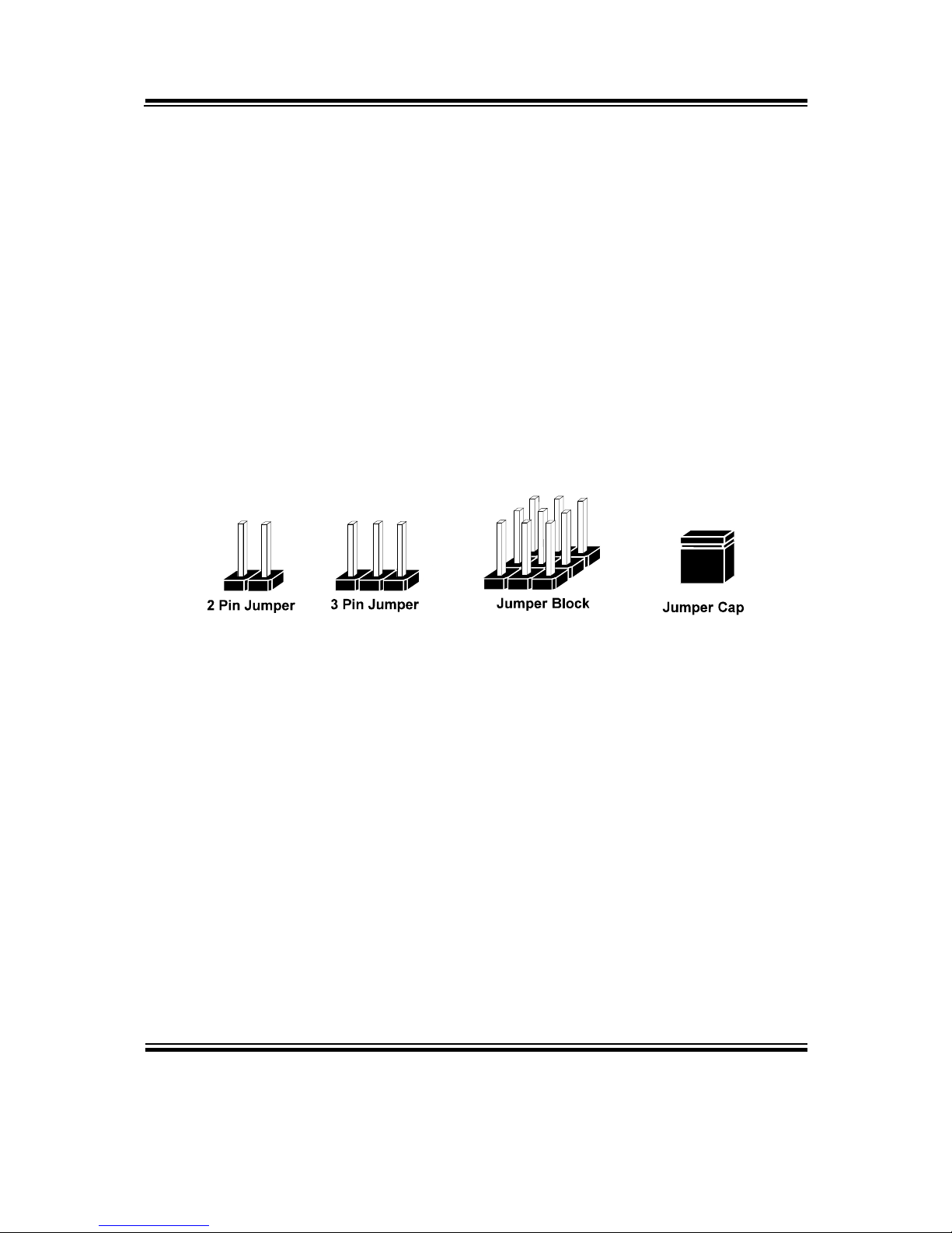
2-3. HOW TO SET THE JUMPERS
You can configure your board by setting jumpers. Jumper is consists of
two or three metal pins with a plastic base mounted on the card, and by
using a small plastic "cap", Also known as the jumper cap (with a metal
contact inside), you are able to connect the pins. So you can set-up your
hardware configuration by "open" or "close" pins.
The jumper can be combined into sets that called jumper blocks. When
the jumpers are all in the block, you have to put them together to set up
the hardware configuration. The figure below shows how this looks like.
JUMPERS AND CAPS
If a jumper has three pins (for examples, labelled PIN1, PIN2, and PIN3),
You can connect PIN1 & PIN2 to create one setting by shorting. You can
either connect PIN2 & PIN3 to create another setting. The same jumper
diagrams are applied all through this manual. The figure below shows
what the manual diagrams look and what they represent.
Page 16
Chapter 2 Hardware Configuration
PMB-892LF USER′S MANUAL
Page: 2-5
JUMPER DIAGRAMS
2 pin Jumper
looks like this
Jumper Cap
looks like this
3 pin Jumper
looks like this
Jumper Block
looks like this
JUMPER SETTINGS
Looks like this
3 pin Jumper
2-3 pin close(enabled)
Looks like this
Jumper Block
1-2 pin close(enabled)
2 pin Jumper close(enabled)
1
1
1
2
1 2
1
1
Looks like this
Page 17
Chapter 2 Hardware Configuration
Page: 2-6
PMB-892LF USER′S MANUAL
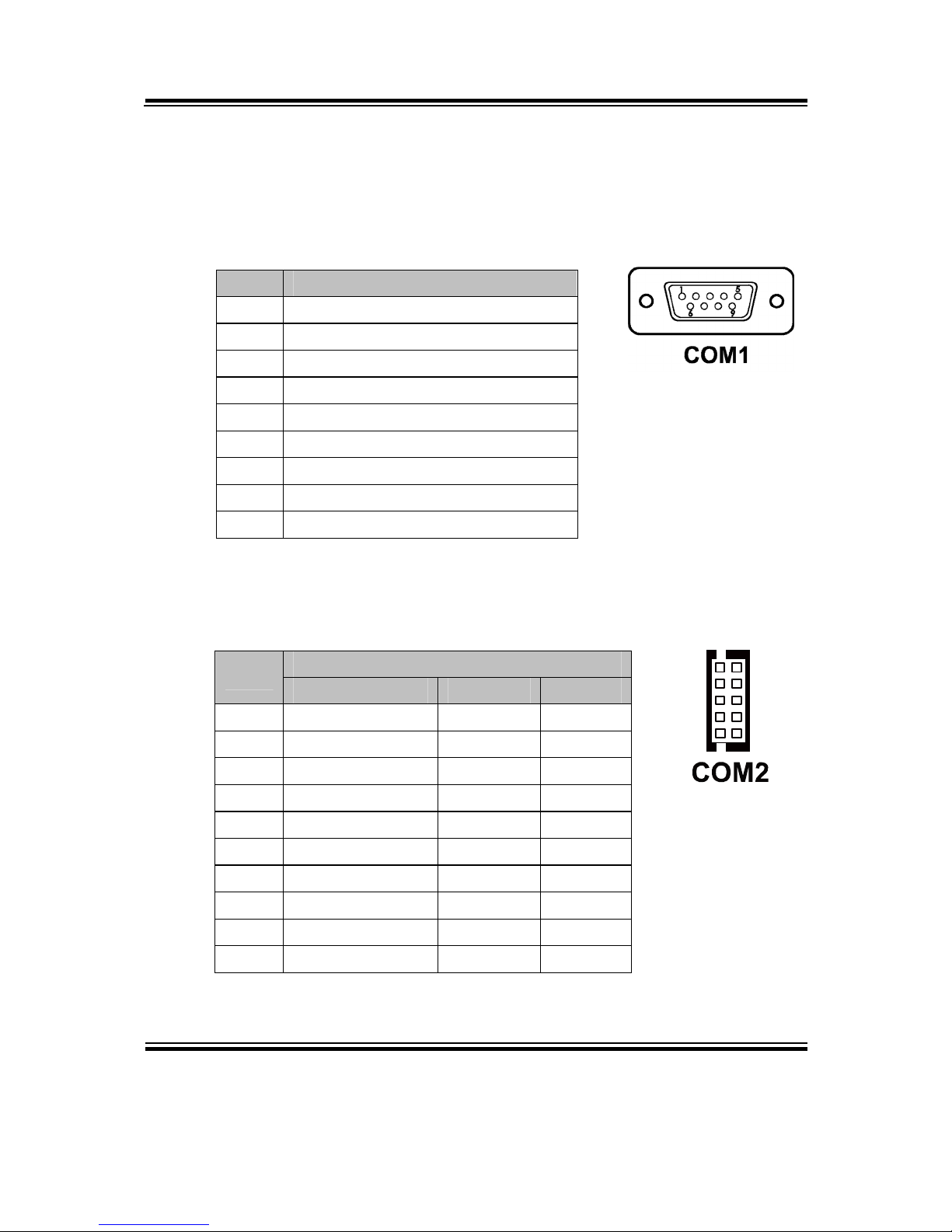
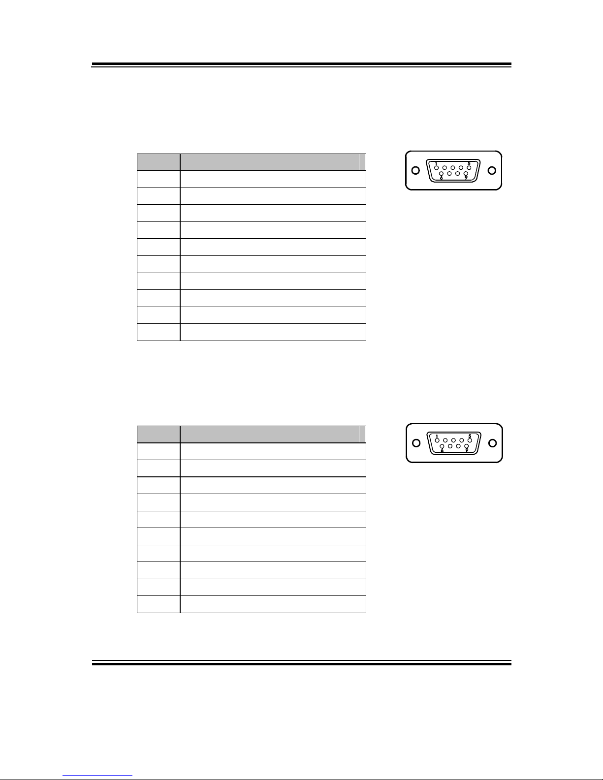
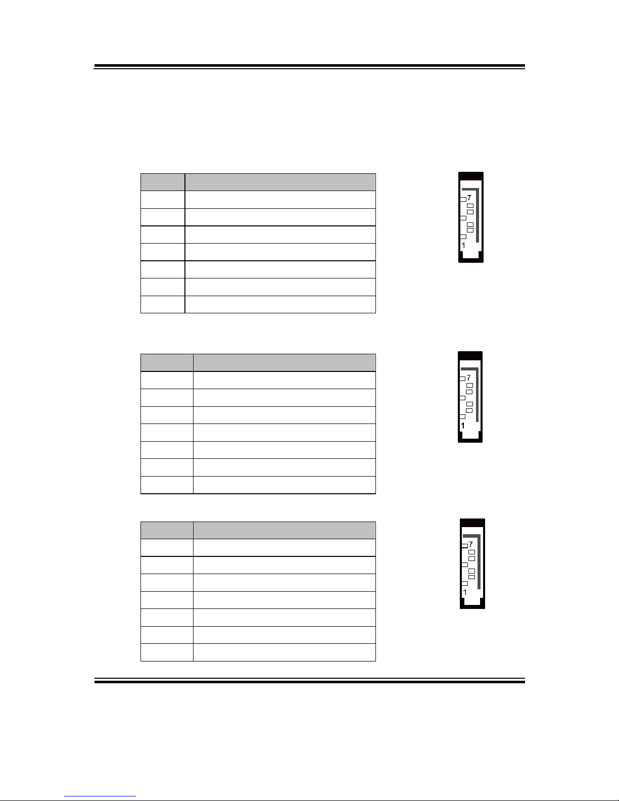
2-4. COM PORT CONNECTOR
COM1: COM1 Connector
COM1 is fixed as RS-232.
The pin assignments are as follows:
PIN ASSIGNMENT
1 COM1_DCD#
2 COM1_RX
3 COM1_TX
4 COM1_DTR#
5 GND
6 COM1_DSR#
7 COM1_RTS#
8 COM1_CTS#
9 COM1_RI#
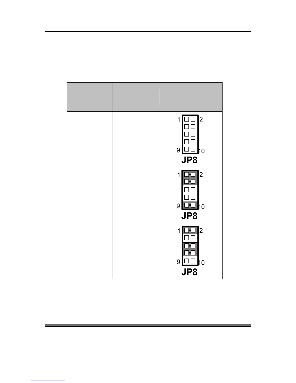
COM2: COM2 Connector
The COM2 is selectable as RS-232/422/485.
The pin assignments are as follows:
ASSIGNMENT
PIN
RS-232 RS-422 RS-485
1 COM2_DCD# TX- 485-
2 COM2_DSR# X X
3 COM2_RX TX+ 485+
4 COM2_RTS# X X
5 COM2_TX RX+ X
6 COM2_CTS# X- X
7 COM2_DTR# RX- X
8 COM2_ RI# X X
9 GND GND GND
10 NC NC NC
9
1
10
2
Page 18
Chapter 2 Hardware Configuration
PMB-892LF USER′S MANUAL
Page: 2-7
COM3: COM3 Connector
COM3 is fixed as RS-232.
The pin assignments are as follows:
PIN ASSIGNMENT
1 COM3_DCD#
2 COM3_RX
3 COM3_TX
4 COM3_DTR#
5 GND
6 COM3_DSR#
7 COM3_RTS#
8 COM3_CTS#
9 COM3_RI#
10 NC
COM4: COM4 Connector
COM4 is fixed as RS-232.
The pin assignments are as follows:
PIN ASSIGNMENT
1 COM4_DCD#
2 COM4_RX
3 COM4_TX
4 COM4_DTR#
5 GND
6 COM4_DSR#
7 COM4_RTS#
8 COM4_CTS#
9 COM4_RI#
10 NC
1
5
6
9
COM3
1
5
6
9
COM4
Page 19
Chapter 2 Hardware Configuration
Page: 2-8
PMB-892LF USER′S MANUAL
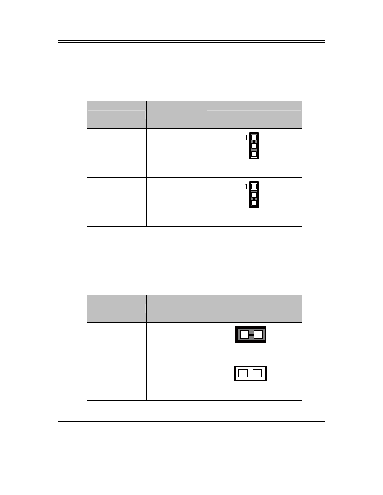
2-5. RS232/422/485 (COM2) SELECTION
JP8: RS232/422/485 (COM2) Selection
This connector is used to set the COM2 function.
The jumper settings are as follows:
COM 2
FUNCTION
JUMPER
SETTINGS
(PIN CLOSED)
JUMPER
ILLUSTRATIONS
RS232 All Open
RS422
1-2
3-4
9-10
RS485
1-2
5-6
7-8
Note: Manufacturing default – RS232
Page 20
Chapter 2 Hardware Configuration
PMB-892LF USER′S MANUAL
Page: 2-9
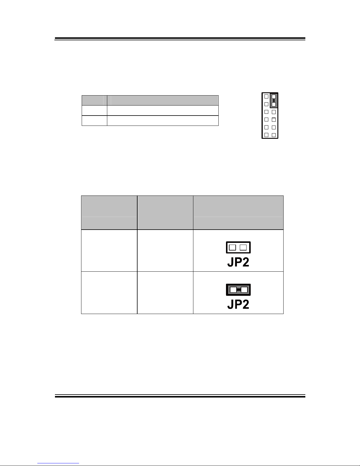
2-6. COM2 AUTO DETECT SELECTION
JP7: COM2 Auto Detect selection
The selections are as follows:
SELECTION
JUMPER
SETTINGS
JUMPER ILLUSTRATION
NORMAL 1-2
JP7
AUTO GATING
2-3
JP7
Note: Manufacturing Default – Normal
2-7. CPU SELECTION
JP9: CPU selection
The selections are as follows:
SELECTION
JUMPER
SETTINGS
JUMPER ILLUSTRATION
Ivy Bridge 1-2
JP9
1
Sandy Bridge open
JP9
1
Note: Manufacturing Default – Ivy Bridge
Page 21
Chapter 2 Hardware Configuration
Page: 2-10
PMB-892LF USER′S MANUAL
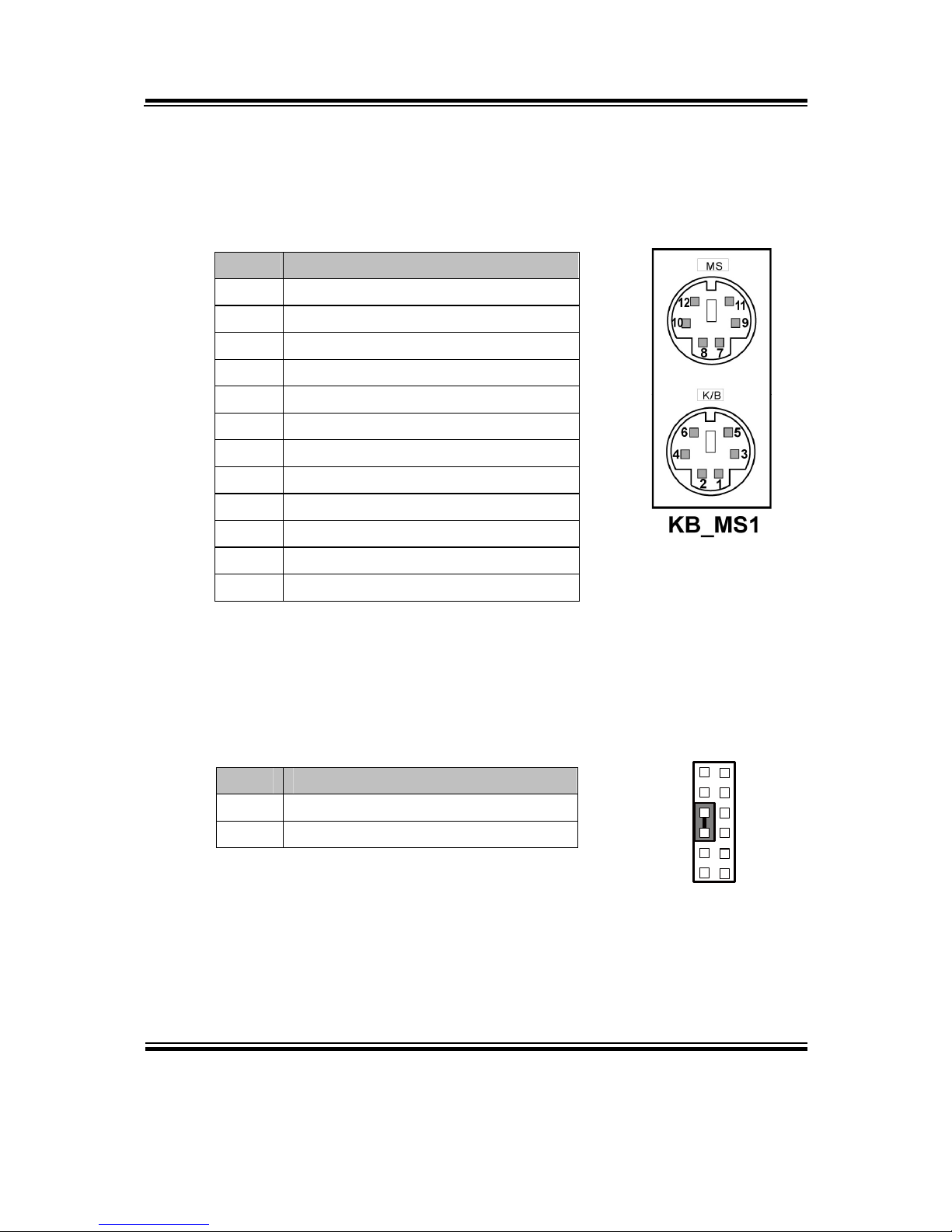
2-8. KEYBOARD & MOUSE CONNECTOR
KB_MS1: Keyboard and PS/2 Mouse Connector
The pin assignments are as follows:
PIN ASSIGNMENT
1 KBDATA
2 NC
3 GND
4 VCC5
5 KBCLK
6 NC
7 MSDATA
8 NC
9 GND
10 VCC5
11 MSCLK
12 NC
2-9. RESET CONNECTOR
FP1 (5, 7): Reset Connector.
The pin assignments are as follows:
PIN ASSIGNMENT
5 GND
7 RST_BTN
1
2
11 12
Reset
FP1
Page 22
Chapter 2 Hardware Configuration
PMB-892LF USER′S MANUAL
Page: 2-11
2-10. HARD DISK DRIVE LED CONNECTOR
FP1 (1, 3): Hard Disk Drive LED Connector
The pin assignments are as follows:
PIN ASSIGNMENT
1 HD_LED+
3 HD_LED-
2-11. ATX POWER BUTTON
FP1 (9, 11): ATX Power Button
The pin assignments are as follows:
PIN ASSIGNMENT
9 PWRBTNSW
11 GND
2-12. EXTERNAL SPEAKER CONNECTOR
FP1 (6, 8, 10, 12): External Speaker Connector
The pin assignments are as follows:
PIN ASSIGNMENT
6 SPK_VCC
8 SPEAKER SIGNAL
10 SPEAKER SIGNAL
12 SPEAKER SIGNAL
1
2
1
1
12
HDDLED
FP1
1 2
11 12
Power
Button
FP1
1
2
1
1
12
Speaker
FP1
Page 23
Chapter 2 Hardware Configuration
Page: 2-12
PMB-892LF USER′S MANUAL
2-13. PLED CONNECTOR
FP1 (2, 4) : PLED Connector
The pin assignments are as follows:
PIN ASSIGNMENT
2 PW_LED+
4 PW_LED-
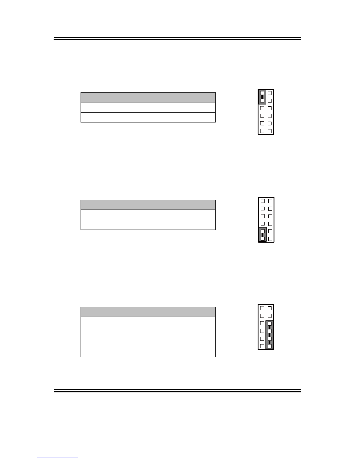
2-14. CLEAR CMOS DATA SELECTION
JP2: Clear CMOS Data Selection
The selections are as follows:
FUNCTION
JUMPER
SETTING
(PIN CLOSED)
JUMPER ILLUSTRATION
Normal Open
1
Clear CMOS* Close
1
Note: Manufacturing Default – Normal
*To clear CMOS data, user must power-off the computer and set the
jumper to “Clear CMOS” as illustrated above. After five to six seconds,
set the jumper back to “Normal” and power-on the computer.
1
2
11 12
Power
LED
FP1
Page 24
Chapter 2 Hardware Configuration
PMB-892LF USER′S MANUAL
Page: 2-13
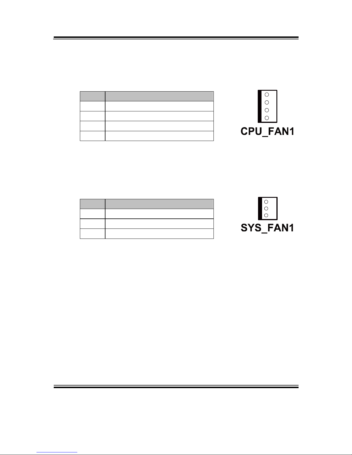
2-15. CPU FAN CONNECTOR
CPU_FAN1: CPU Fan connector
The pin assignments are as follows:
PIN ASSIGNMENT
1 GND
2 VCC12
3 FAN_TAC1
4 FAN_CTL1
2-16. SYSTEM FAN CONNECTOR
SYS_FAN1: System Fan connector
The pin assignments are as follows:
PIN ASSIGNMENT
1 GND
2 VCC12
3 LPC1_FANIO2
1
4
1
3
Page 25
Chapter 2 Hardware Configuration
Page: 2-14
PMB-892LF USER′S MANUAL
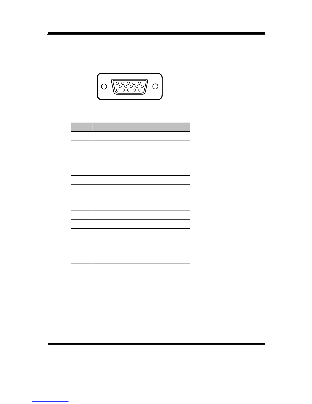
2-17. VGA CONNECTOR
VGA1: VGA Connector
1
5
6
10
11
15
VGA1
PIN ASSIGNMENT
1 CRTRED
2 CRTGREEN
3 CRTBLUE
4 NC
5 GND
6 CRT_ALWAYS_ON
7 GND
8 GND
9 CRTVCC_L
10 GND
11 NC
12 CRTDATA
13 HSYNC
14 VSYNC
15 CRTCLK
Page 26
Chapter 2 Hardware Configuration
PMB-892LF USER′S MANUAL
Page: 2-15
2-18. SERIAL ATA CONNECTOR
SATA1, SATA2, SATA4: Three Serial ATA Connectors
The pin assignments are as follows:
SATA1:
PIN ASSIGNMENT
1 GND
2 SATA_TXPC0
3 SATA_TXNC0
4 GND
5 SATA_RXNC0
6 SATA_RXPC0
7 GND
SATA2:
PIN ASSIGNMENT
1 GND
2 SATA_TXPC1
3 SATA_TXNC1
4 GND
5 SATA_RXNC1
6 SATA_RXPC1
7 GND
SATA3:
PIN ASSIGNMENT
1 GND
2 SATA_TXPC3
3 SATA_TXNC3
4 GND
5 SATA_RXNC3
6 SATA_RXPC3
7 GND
S
ATA1
SATA2
S
AT
A3
Page 27

Chapter 2 Hardware Configuration
Page: 2-16
PMB-892LF USER′S MANUAL
SATA4:
PIN ASSIGNMENT
1 GND
2 SATA_TXPC4
3 SATA_TXNC4
4 GND
5 SATA_RXNC4
6 SATA_RXPC4
7 GND
S
ATA4
Page 28

Chapter 2 Hardware Configuration
PMB-892LF USER′S MANUAL
Page: 2-17
2-19. PRINTER CONNECTOR
LPT1: Printer Connector
As to link the Printer to the card, you need a cable to connect both DB25
connector and parallel port.
The pin assignments are as follow:
LPT1
PIN ASSIGNMENT PIN ASSIGNMENT
1 STB 14 AFD#
2 PDR0 15 ERR#
3 PDR1 16 INIT#
4 PDR2 17 SLIN#
5 PDR3 18 GND
6 PDR4 19 GND
7 PDR5 20 GND
8 PDR6 21 GND
9 PDR7 22 GND
10 ACK# 23 GND
11 BUSY 24 GND
12 PE 25 GND
13 SLCT 26 NC
Page 29
Chapter 2 Hardware Configuration
Page: 2-18
PMB-892LF USER′S MANUAL
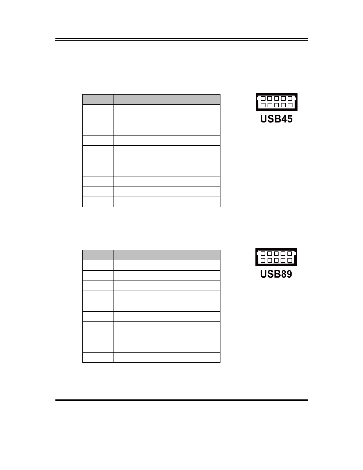
2-20. UNIVERSAL SERIAL BUS CONNECTOR
USB45: Universal Serial Bus Connector
The pin assignments are as follows:
PIN ASSIGNMENT
1 USB_45_VCC5
2 USB_45_VCC5
3 USBN4
4 USBN5
5 USBP4
6 USBP5
7 GND
8 GND
9 GND
10 GND
USB89: Universal Serial Bus Connector
The pin assignments are as follows:
PIN ASSIGNMENT
1 USB_89_VCC5
2 USB_89_VCC5
3 USBN8
4 USBN9
5 USBP8
6 USBP9
7 GND
8 GND
9 GND
10 GND
1
9
2
10
1
9
2
10
Page 30

Chapter 2 Hardware Configuration
PMB-892LF USER′S MANUAL
Page: 2-19
2-21. USB & LAN CONNECTOR
LAN1_USB1: USB & LAN Connector
The pin assignments are as follows:
LAN Signal:
PIN ASSIGNMENT
1 VCC_LAN1
2 LAN1_MDI_0P
3 LAN1_MDI_0N
4 LAN1_MDI_1P
5 LAN1_MDI_1N
6 LAN1_MDI_2P
7 LAN1_MDI_2N
8 LAN1_MDI_3P
9 LAN1_MDI_3N
10 COM_LAN1
LAN LED Indicator:
Left Side LED
RED Color On Giga LAN Speed Indicator
Off No LAN switch/ hub connected.
Right Side LED
Orange Color Blinking LAN Message Active
Off No LAN Message Active
USB Signal:
PIN ASSIGNMENT PIN ASSIGNMENT
A1 VCCUSB1 B1 VCCUSB1
A2 USBP0N B2 USBP1N
A3 USBP0P B3 USBP1P
A4 GND B4 GND
A5 USB3_RX1_DN B5 USB3_RX2_DN
A6 USB3_RX1_DP B6 USB3_RX2_DP
A7 GND B7 GND
A8 USB3_TX1_DN B8 USB3_TX2_DN
A9 USB3_TX1_DP B9 USB3_TX2_DP
Yellow
Gree
n
B1 B4
B9 B5
A1 A4
A9 A5
10 1
Page 31

Chapter 2 Hardware Configuration
Page: 2-20
PMB-892LF USER′S MANUAL
LAN2_USB1: USB & LAN Connector
The pin assignments are as follows
:
LAN Signal:
PIN ASSIGNMENT
1 VCC_LAN2
2 LAN2_MDI_0P
3 LAN2_MDI_0N
4 LAN2_MDI_1P
5 LAN2_MDI_1N
6 LAN2_MDI_2P
7 LAN2_MDI_2N
8 LAN2_MDI_3P
9 LAN2_MDI_3N
10 COM_LAN2
LAN LED Indicator:
Left Side LED
RED Color On Giga LAN Speed Indicator
Off No LAN switch/ hub connected.
Right Side LED
Orange Color Blinking
LAN Message Active
Off No LAN Message Active
USB Signal:
PIN ASSIGNMENT PIN ASSIGNMENT
A1 VCCUSB2 B1 VCCUSB2
A2 USBP2N B2 USBP3N
A3 USBP2P B3 USBP3P
A4 GND B4 GND
A5 USB3_RX3_DN B5 USB3_RX4_DN
A6 USB3_RX3_DP B6 USB3_RX4_DP
A7 GND B7 GND
A8 USB3_TX3_DN B8 USB3_TX4_DN
A9 USB3_TX3_DP B9 USB3_TX4_DP
Yellow
Gree
n
B1 B4
B9 B5
A1 A4
A9 A5
10 1
Page 32

Chapter 2 Hardware Configuration
PMB-892LF USER′S MANUAL
Page: 2-21
2-22. DISPLAY PORT CONNECTOR
JDP1: Display Port Connector
The pin assignments are as follows:
PIN ASSIGNMENT PIN ASSIGNMENT
1 DP_C_DATA0+ 2 GND
3 DP_C_DATA0- 4 DP_C_DATA1+
5 GND 6 DP_C_DATA1-
7 DP_C_DATA2+ 8 GND
9 DP_C_DATA2- 10 DP_C_DATA3+
11 GND 12 DP_C_DATA3-
13 DP_C_AUX_ENJ 14 GND
15 DP_C_AUX+ 16 DP_C_HPD
17 DP_C_AUX- 18 DP_VCC3_3
19 DP_VCC5 20 DP_VCC3_3
2-23. DIGITAL INPUT/OUTPUT CONNECTOR
DIO1: Digital I/O Connector
The pin assignments are as follows:
PIN ASSIGNMENT PIN ASSIGNMENT
1 VCC5 2 GND
3 DIN0 4 DOUT0
5 DIN1 6 DOUT1
7 DIN2 8 DOUT2
9 DIN3 10 DOUT3
1 2
109
DIO1
Page 33

Chapter 2 Hardware Configuration
Page: 2-22
PMB-892LF USER′S MANUAL
2-24. ATX POWER CONNECTOR
ATX_PWR1: ATX Power Connector
The pin assignments are as follows:
PIN ASSIGNMENT PIN ASSIGNMENT
1 +3.3V 13 +3.3V
2 +3.3V 14 -12V
3 GND 15 GND
4 +5V 16 PSON
5 GND 17 GND
6 +5V 18 GND
7 GND 19 GND
8 POK 20 -5V
9 5VSB 21 +5V
10 +12V 22 +5V
11 +12V 23 +5V
12 +3.3V 24 GND
ATX_PWR2: ATX Power Connector
The pin assignments are as follows:
PIN ASSIGNMENT
1 GND
2 GND
3 +12V
4 +12V
A
TX_PWR1
ATX_PWR2
Page 34

Chapter 2 Hardware Configuration
PMB-892LF USER′S MANUAL
Page: 2-23
2-25. SOUND CONNECTOR
AUDIO1: Sound Connector, including Line-In, Line-Out & Mic. Also
can support only MIC connector. The pin assignments are as follows:
Line-In
PIN ASSIGNMENT
32 HD_LINE-L
33 GND
34 GND
35 HD_LINE-R
Line-Out
PIN ASSIGNMENT
22 HD_OUT-L
23 NC
24 NC
25 HD_OUT-R
MIC-In
PIN ASSIGNMENT
1 GND
2 HD_MIC1
3 HD_MIC_GND
4 NC
5 HD_MIC_VCC
SPDIF (Optional, the same port with Line-In)
PIN ASSIGNMENT
42 GND
43 VCC_AUD
44 SPDIF OUT
AUDIO1
1 2345
22232425
32333435
424344
Page 35

Page: 3-1
SOFTWARE
UTILITIES
This chapter comprises the detailed information of VGA driver,
LAN driver, and Sound driver.
Section includes:
Intel® Chipset Software Installation Utility
VGA Driver Utility
LAN Driver Utility
SOUND Driver Utility
CHAPTER
3
Page 36

Chapter 3 Software Utilities
Page:3-2
PMB-892LF USER′S MANUAL
3-1. INTRODUCTION
Enclosed with our PMB-892LF package, you will find a CD ROM disk
containing all types of drivers we have. As a PMB-892LF user, you will only
need the some of files contained in the CD ROM disk, please take note of the
following chart:
FILE NAME
(Assume that CD ROM drive is D:)
PURPOSE
D:\Driver\FLASH For Aptio (EFI) BIOS update utility
D:\Driver\Utility Intel® Chipset Device Software
Installation Utility
D:\Driver\VGA Intel® HD Graphics Family for VGA
driver installation
D:\Driver\LAN Intel® 82579LM and 82583V for
LAN driver installation
D:\Driver\Sound Realtek® ALC888S for Sound driver
installation
D:\Driver\ME
For Intel® Management Engine
Interface
D:\Driver\USB3
Intel® USB 3.0 eXtensible Host
Controller
D:\Driver\Intel® RST
Intel® Matrix Storage Manager
Utility.
D:\Driver\F6Floppy Intel® F6 Floppy Utility.
Note: Remember to install the Utility right after the OS is fully installed.
Page 37

Chapter 3 Software Utilities
PMB-892LF USER′S MANUAL
Page:3-3
3-2. INTEL® CHIPSET SOFTWARE INSTALLATION UTILITY
3-2-1. Introduction
The Intel® Chipset Device Software installs Windows* INF files to the
target system. These files outline to the operating system how to
configure the Intel® chipset components in order to ensure that the
following features function properly:
- PCIe Support
- SATA Storage Support
- USB Support
- Identification of Intel® Chipset Components in the Device Manager
3-2-2. Installation of Utility for Windows XP/Vista/7
The Utility Pack is to be installed only for Windows XP, Windows Vista,
and Windows 7 program.
It should be installed right after the OS installation, kindly follow the
following steps:
1. Insert the Utility Disk into Floppy Disk Drive A/B or CD ROM
drive.
2. Under Windows system, go to the directory where Utility Disc is
located. e.g. :\DRIVER\UTILITY\infinst_autol.exe
3. Click infinst_autol.exe file for utility installation.
4. Follow the instructions on the screen to complete the installation.
5. Once installation is completed, shut down the system and restart in
order for the changes to take effect.
Page 38

Chapter 3 Software Utilities
Page:3-4
PMB-892LF USER′S MANUAL
3-3. VGA DRIVER UTILITY
The VGA interface is embedded with our PMB-892LF system to support CRT
display. The following illustration briefly shows you the content of VGA
driver in D:\Driver\VGA.
3-3-1. Installation of VGA Driver
1. Start the computer (Win XP/Vista/7).
2. Insert the Utility Disk into the CD ROM drive or drive A/B.
3. Open the VGA folder, for your system to choose an appropriate folder, and
double-click "exe" file to install. e.g. D:\DRIVER\VGA\Your system\
***.exe
(If D is not your CD-ROM drive, substitute D with the correct drive letter.)
4. Follow the Wizard's on-screen instructions to complete the installation.
Page 39

Chapter 3 Software Utilities
PMB-892LF USER′S MANUAL
Page:3-5
3-4. LAN DRIVER UTILITY
3-4-1. Introduction
The PMB-892LF is enhanced with LAN function that can support
various network adapters. The content of the LAN driver is found as
follows:
1. Win XP program
2. Win Vista program
3. Win 7 program
For more details on Installation procedure, please refer to Readme.txt
file found on LAN DRIVER UTILITY.
Page 40

Chapter 3 Software Utilities
Page:3-6
PMB-892LF USER′S MANUAL
3-5. SOUND DRIVER UTILITY
3-5-1. Introduction
The Audio chip enhanced in this system is fully compatible with
Windows XP, Windows Vista and Windows 7. Below, you will find the
content of the Sound driver:
3-5-2. Installation Procedure for Windows XP/Vista/7
1. Open the SOUND folder. For your system to choose an appropriate folder,
and Run the setup.exe program to start the installation.
e.g. D:\DRIVER\SOUND\Your system\setup.exe
(If D is not your CD-ROM drive, substitute D with the correct drive letter.)
2. Click on [Next] to continue the procedure. If the Windows popup
"Windows can't verify the publisher of this driver software" message, press
"Install this driver software anyway" to continue the installation.
3. Finally, select to restart the system and press [Finish] to complete the
installation.
Page 41

Chapter 3 Software Utilities
PMB-892LF USER′S MANUAL
Page:3-7
3-6. INTEL® ME DRIVER UTILITY
3-6-1. Introduction
The Intel® ME components including the Intel® Management and Security
Status Application. The content of the ME driver is found as follows:
For more details on Installation procedure, please refer to Readme.txt
file found on ME DRIVER UTILITY.
Page 42

Chapter 3 Software Utilities
Page:3-8
PMB-892LF USER′S MANUAL
3-7. USB3.0 SOFTWARE INSTALLATION UTILITY
3-7-1. Installation of Utility for Windows XP
General Installation Notes:
1. The operating system must be installed prior to the installation of the driver.
2. This installation procedure is specific only to the version of driver and
installation file included in this release.
3. This procedure assumes that all of the software associated with this release is
located in the same directory.
For more details on Installation procedure, please refer to Readme.txt
file found on Intel USB 3.0 DRIVER UTILITY.
Page 43

Page: 4-1
AMI
BIOS SETUP
This chapter shows how to set up the AMI BIOS.
Section includes:
Introduction
Entering Setup
Main
Advanced
Chipset
Boot
Security
Save & Exit
CHAPTER
4
Page 44

Chapter 4 AMI BIOS Setup
Page: 4-2
PMB-892LF USER′S MANUAL
4-1. INTRODUCTION
The board PMB-892LF uses an AMI Aptio BIOS that is stored in the Serial
Peripheral Interface Flash Memory (SPI Flash) and can be updated. The SPI
Flash contains the BIOS Setup program, Power-on Self-Test (POST), the PCI
auto-configuration utility, LAN EEPROM information, and Plug and Play
support.
Aptio is AMI’s BIOS firmware based on the UEFI (Unified Extensible Firmware
Interface) Specifications and the Intel Platform Innovation Framework for EFI.
The UEFI specification defines an interface between an operating system and
platform firmware. The interface consists of data tables that contain platformrelated information, boot service calls, and runtime service calls that are available
to the operating system and its loader. These provide standard environment for
booting an operating system and running pre-boot applications.
Following illustration shows Extensible Firmware Interface’s position in the
software stack.
Page 45

Chapter 4 AMI BIOS Setup
PMB-892LF USER′S MANUAL
Page: 4-3
EFI BIOS provides an user interface allow users the ability to modify hardware
configuration, e.g. change system date and time, enable or disable a system
component, decide bootable device priorities, setup personal password, etc.,
which is convenient for modifications and customization of the computer system
and allows technicians another method for finding solutions if hardware has any
problems.
The BIOS Setup program can be used to view and change the BIOS settings for
the computer. The BIOS Setup program is accessed by pressing the <Del> or
<F2> key after the POST memory test begins and before the operating system
boot begins. The settings are shown below.
Page 46

Chapter 4 AMI BIOS Setup
Page: 4-4
PMB-892LF USER′S MANUAL
4-2. ENTERING SETUP
When the system is powered on, the BIOS will enter the Power-On Self Test
(POST) routines and the following message will appear on the lower screen:
POST screen
As long as this message is present on the screen you may press the <Del>
key (the one that shares the decimal point at the bottom of the number
keypad) to access the Setup program. In a moment, the main menu of the
Aptio Setup Utility will appear on the screen:
Page 47

Chapter 4 AMI BIOS Setup
PMB-892LF USER′S MANUAL
Page: 4-5
Setup program initial screen
You may move the cursor by up/down keys to highlight the individual menu items.
As you highlight each item, a brief description of the highlighted selection will
appear at the bottom of the screen.
Page 48

Chapter 4 AMI BIOS Setup
Page: 4-6
PMB-892LF USER′S MANUAL
4-3. Main
Main screen
BIOS Setting Options Description/Purpose
BIOS Vendor No changeable options Displays the BIOS vendor.
Core Version No changeable options Displays the current BIOS core version.
Compliancy No changeable options Displays the current UEFI version.
Project Version No changeable options Displays the version of the BIOS
currently installed on the platform.
Build Date No changeable options Displays the date of current BIOS
version.
System Date month, day, year Specifies the current date.
System Time hour, minute, second Specifies the current time.
Access Level No changeable options Displays the current user level.
Page 49

Chapter 4 AMI BIOS Setup
PMB-892LF USER′S MANUAL
Page: 4-7
4-4. Advanced
Advanced screen
BIOS Setting Options Description/Purpose
ACPI Settings Sub-Menu System ACPI Parameters.
CPU Configuration Sub-Menu CPU Configuration. Parameters.
SATA Configuration Sub-Menu SATA Configuration Parameters.
USB Configuration Sub-Menu USB Configuration Parameters.
W83627UHG Super
IO Configuration
Sub-Menu System Super IO Chip Parameters.
W83627UHG HW
Monitor
Sub-Menu Monitor hardware status
WatchDog
Configuration
Sub-Menu Set System WatchDog Parameters.
CPU PPM
Configuration
Sub-Menu CPU PPM Configuration
Page 50

Chapter 4 AMI BIOS Setup
Page: 4-8
PMB-892LF USER′S MANUAL
4-4-1. Advanced – APCI Subsystems Settings
ACPI Settings screen
BIOS Setting Options Description/Purpose
Enable
Hibernation
- Disabled
- Enabled
Enables or Disables System ability to Hibernate
(OS/S4 Sleep State). This option may be not
effective with some OS.
ACPI Sleep
State
- Suspend
Disabled
- S1 (CPU Stop
Clock)
- S3 (Suspend to
RAM)
- Both S1 and S3
available
for OS to
choose from
Specifies the ACPI sleep state.
Suspend Disabled disables ACPI sleep feature.
S1 mode allows the CPU enter Stop Clock
mode to stop executing instructions.
S3 allows the platform to enter Suspend to
RAM mode.
Both S1 and S3 available for OS to choose
from allows the OS to choose the sleep state
type.
Page 51

Chapter 4 AMI BIOS Setup
PMB-892LF USER′S MANUAL
Page: 4-9
4-4-2. Advanced – CPU Configuration
CPU Configuration screen
BIOS Setting Options Description/Purpose
CPU Signature No changeable options Reports the CPU Signature
Microcode Patch No changeable options Reports the CPU Microcode Patch
Version.
Max CPU Speed No changeable options Reports the Max CPU Speed.
Min CPU Speed No changeable options Reports the Min CPU Speed
Processor Cores No changeable options Displays number of physical cores in
processor.
Intel HT
Technology
No changeable options Reports if Intel Hyper-Threading
Technology is supported by processor
Intel VT-x
Technology
No changeable options Reports if Intel VT-x Technology is
supported by processor.
Intel SMX No changeable options Reports if Intel SMX Technology is
Page 52

Chapter 4 AMI BIOS Setup
Page: 4-10
PMB-892LF USER′S MANUAL
BIOS Setting Options Description/Purpose
Technology supported by processor.
L1 Data Cache No changeable options Displays size of L1 Data Cache
L1 Code Cache No changeable options Displays size of L1 Code Cache
L2 Cache No changeable options Displays size of L2 Cache.
L3 Cache No changeable options Displays size of L3 Cache.
Hyper-threading - Disabled
- Enabled
Enable or disable Hyper-Threading
technology.
Active Processor
Cores
- All
- 1
- 2
- 3
Indicates the number of cores to enable
in processor.
Limit CPUID
Maximum
- Disabled
- Enabled
Enables for legacy operating systems to
boot processors with extended CPUID
functions.
Intel Virtualization
Technology
-Disabled
-Enabled
When enabled, a VMM can utilize the
additional hardware capabilities
provided by Vander pool Technology.
Page 53

Chapter 4 AMI BIOS Setup
PMB-892LF USER′S MANUAL
Page: 4-11
4-4-3. Advanced – SATA Configuration
SATA Configuration screen
BIOS Setting Options Description/Purpose
SATA
Controller(s)
- Disabled
- Enabled
Enable or disable SATA Device.
SATA Mode
Selection
- IDE
- AHCI
- RAID
Configures SATA as IDE, AHCI or RAID
mode.
SATA 1~4 [drive] Displays the drive installed on this SATA
port. Shows [Empty] if no drive is installed.
mSATA [drive] Displays the drive installed on this mSATA
port. Shows [Empty] if no drive is installed.
Note: Please configure the Mini PCI-E
function as “mSATA” for this function.
Page 54

Chapter 4 AMI BIOS Setup
Page: 4-12
PMB-892LF USER′S MANUAL
Select [AHCI] mode and there are some more items as below:
SATA Configuration - RAID Mode screen
BIOS Setting Options Description/Purpose
Aggressive LPM
Support
- Disabled
- Enabled
Enable PCH to aggressively enter link
power state.
SATA Controller
Speed
- Gen1
- Gen2
- Gen3
Indicates the maximum speed the SATA
controller can support.
Software Feature
Mask Configuration
Sub-menu RAID OROM/RST driver will refer to the
SWFM configuration to enable or disable
the storage features.
Port 0 - 5 - Disabled
- Enabled
Enables or disable SATA port.
Hot Plug - Disabled
- Enabled
Designates this port as Hot Pluggable.
Page 55

Chapter 4 AMI BIOS Setup
PMB-892LF USER′S MANUAL
Page: 4-13
BIOS Setting Options Description/Purpose
External SATA - Disabled
- Enabled
External SATA Support.
SATA Device Type - Hard Disk Driver
- Solid State Drive
Identify the SATA port is connected to
Solid State Drive or Hard Disk Drive.
Spin Up Device - Disabled
- Enabled
On an edge detect from 0 to 1, the PCH
starts a COMRESET initialization
sequence to the device.
Page 56

Chapter 4 AMI BIOS Setup
Page: 4-14
PMB-892LF USER′S MANUAL
SATA Configuration - AHCI Mode - Software Feature Mask Configuration screen
BIOS Setting Options Description/Purpose
RAID0 - Disabled
- Enabled
Enable or disable RAID 0 feature.
RAID1 - Disabled
- Enabled
Enable or disable RAID 1 feature.
RAID10 - Disabled
- Enabled
Enable or disable RAID 10 feature.
RAID5 - Disabled
- Enabled
Enable or disable RAID 5 feature.
Page 57

Chapter 4 AMI BIOS Setup
PMB-892LF USER′S MANUAL
Page: 4-15
Select [RAID] mode it have some more items as below:
SATA Configuration - RAID Mode screen
BIOS Setting Options Description/Purpose
Aggressive LPM
Support
- Disabled
- Enabled
Enable PCH to aggressively enter link
power state.
SATA Controller
Speed
- Gen1
- Gen2
- Gen3
Indicates the maximum speed the SATA
controller can support.
Software Feature
Mask Configuration
Sub-menu RAID OROM/RST driver will refer to the
SWFM configuration to enable or disable
the storage features.
Alternate ID - Enabled
- Disabled
Report alternate Device ID
Page 58

Chapter 4 AMI BIOS Setup
Page: 4-16
PMB-892LF USER′S MANUAL
BIOS Setting Options Description/Purpose
Port 0 - 5 - Disabled
- Enabled
Enables or disable SATA port.
Hot Plug - Disabled
- Enabled
Designates this port as Hot Pluggable.
External SATA - Disabled
- Enabled
External SATA Support.
SATA Device Type - Hard Disk Driver
- Solid State Drive
Identify the SATA port is connected to
Solid State Drive or Hard Disk Drive.
Spin Up Device - Disabled
- Enabled
On an edge detect from 0 to 1, the PCH
starts a COMRESET initialization sequence
to the device.
Page 59

Chapter 4 AMI BIOS Setup
PMB-892LF USER′S MANUAL
Page: 4-17
4-4-4. Advanced – USB Configuration
USB Configuration Screen
BIOS Setting Options Description/Purpose
USB Devices No changeable options Displays number of available USB
devices.
Legacy USB
Support
- Enabled
- Disabled
- Auto
Enables support for legacy USB.
USB 3.0 Support - Enabled
- Disabled
Enable/Disable USB3.0 (XHCI)
controller support.
XHCI Hand-off - Enabled
- Disabled
This is a workaround for OSes without
XHCI hand-off support.
EHCI Hand-off - Disabled
- Enabled
This is a workaround for OSes w/o
EHCI hand-off support.
Page 60

Chapter 4 AMI BIOS Setup
Page: 4-18
PMB-892LF USER′S MANUAL
4-4-5. Advanced – W83627UHG Super IO Configuration
W83627UHG Super IO Configuration Screen
BIOS Setting Options Description/Purpose
W83627UHG
Super IO Chip
No changeable options Displays the super IO chip model and
its manufacturer.
COM 1 Sub-menu Set Parameters for COM 1
COM 2 Sub-menu Set Parameters for COM 2
COM 3 Sub-menu Set Parameters for COM 3
COM 4 Sub-menu Set Parameters for COM 4
Parallel Port
Configuration
Sub-menu Set Parameters for Parallel Port.
Page 61

Chapter 4 AMI BIOS Setup
PMB-892LF USER′S MANUAL
Page: 4-19
W83627UHG Super IO Configuration - Serial Port 0 Configuration screen
BIOS Setting Options Description/Purpose
Serial Port - Disabled
- Enabled
Enable/Disable COM 1.
Device Settings No changeable options Reports the current COM 1 setting.
Change Settings - Auto
- IO=3F8h; IRQ=4
- IO=3F8h;
IRQ=3,4,5,6,7,10,11,12
- IO=2F8h;
IRQ=3,4,5,6,7,10,11,12
- IO=3E8h;
IRQ=3,4,5,6,7,10,11,12
- IO=2E8h;
IRQ=3,4,5,6,7,10,11,12
Specifies the base I/O address and
interrupt request for the serial port 0
if enabled.
Page 62

Chapter 4 AMI BIOS Setup
Page: 4-20
PMB-892LF USER′S MANUAL
W83627UHG Super IO Configuration - Serial Port 1 Configuration
BIOS Setting Options Description/Purpose
Serial Port -Disabled
-Enabled
Enable/Disable COM 2.
Device Settings No changeable options Reports the current COM 2 setting.
Change Settings - Auto
- IO=2F8h; IRQ=3
- IO=3F8h;
IRQ=3,4,5,6,7,10,11,12
- IO=2F8h;
IRQ=3,4,5,6,7,10,11,12
- IO=3E8h;
IRQ=3,4,5,6,7,10,11,12
- IO=2E8h;
IRQ=3,4,5,6,7,10,11,12
Specifies the base I/O address and
interrupt request for the serial port 1 if
enabled.
Page 63

Chapter 4 AMI BIOS Setup
PMB-892LF USER′S MANUAL
Page: 4-21
W83627UHG Super IO Configuration - Serial Port 2 Configuration screen
BIOS Setting Options Description/Purpose
Serial Port -Disabled
-Enabled
Enable/Disable COM 3.
Device Settings No changeable options Reports the current COM 3 setting.
Change Settings - Auto
- IO=3E8h; IRQ=7
- IO=3F8h;
IRQ=3,4,5,6,7,10,11,12
- IO=2F8h;
IRQ=3,4,5,6,7,10,11,12
- IO=3E8h;
IRQ=3,4,5,6,7,10,11,12
- IO=2E8h;
IRQ=3,4,5,6,7,10,11,12
Specifies the base I/O address and
interrupt request for the serial port 2
if enabled.
Page 64

Chapter 4 AMI BIOS Setup
Page: 4-22
PMB-892LF USER′S MANUAL
W83627UHG Super IO Configuration - Serial Port 3 Configuration screen
BIOS Setting Options Description/Purpose
Serial Port -Disabled
-Enabled
Enable/Disable COM 4.
Device Settings No changeable options Reports the current COM 4 setting.
Change Settings - Auto
- IO=2E8h; IRQ=10
- IO=3F8h;
IRQ=3,4,5,6,7,10,11,12
- IO=2F8h;
IRQ=3,4,5,6,7,10,11,12
- IO=3E8h;
IRQ=3,4,5,6,7,10,11,12
- IO=2E8h;
IRQ=3,4,5,6,7,10,11,12
Specifies the base I/O address and
interrupt request for the serial port 3 if
enabled.
Page 65

Chapter 4 AMI BIOS Setup
PMB-892LF USER′S MANUAL
Page: 4-23
W83627UHG Super IO Configuration - Parallel Port Configuration screen
BIOS Setting Options Description/Purpose
Parallel Port - Disabled
- Enabled
Configures the parallel port.
Device Settings No changeable options Reports the current parallel port setting.
Change Settings - Auto
- IO=378h; IRQ=5
- IO=378h;
IRQ=5,6,7,10,11,12
- IO=278h;
IRQ=5,6,7,10,11,12
- IO=3BCh;
IRQ=5,6,7,10,11,12
- IO=378h;
- IO=278h;
- IO=3BCh;
Specifies the base I/O address and
interrupt request for the parallel port if
enabled.
Page 66

Chapter 4 AMI BIOS Setup
Page: 4-24
PMB-892LF USER′S MANUAL
BIOS Setting Options Description/Purpose
Device Mode - STD Printer Mode
- SPP Mode
- EPP-1.9 and SPP
Mode
- EPP-1.7 and SPP
Mode
- ECP Mode
- ECP and EPP 1.9
Mode
- ECP and EPP 1.7
Mode
Selects the mode for the parallel port.
Not available if the parallel port is
disabled.
SPP is Standard Parallel Port mode, a
bi-directional mode for printers.
EPP is Enhanced Parallel Port mode, a
high-speed bi-directional mode for nonprinter peripherals.
ECP is Enhanced Capability Port mode,
a high-speed bi-directional mode for
printers and scanners.
Page 67

Chapter 4 AMI BIOS Setup
PMB-892LF USER′S MANUAL
Page: 4-25
4-4-6. Advanced – HW Monitor
HW Monitor Screen
BIOS Setting Options Description/Purpose
Smart Fan Mode
Configuration
Sub-menu Smart Fan Mode select.
System
Temperature
No changeable options Displays temperature in the remote
thermal sensor zone.
CPU Temperature No changeable options Displays processor's temperature.
SysFan Speed No changeable options Displays fan speed of the chassis fan.
CpuFan Speed No changeable options Displays fan speed of the CPU fan.
Vcore No changeable options Displays voltage level of the +Vcore in
supply.
+12V No changeable options Displays voltage level of the +12V in
Page 68

Chapter 4 AMI BIOS Setup
Page: 4-26
PMB-892LF USER′S MANUAL
BIOS Setting Options Description/Purpose
supply.
+1.5V No changeable options Displays voltage level of the +1.5V in
supply.
+1.05V No changeable options Displays voltage level of the +1.05V in
supply.
AVCC No changeable options Displays voltage level of the +5V in
supply.
5Vcc No changeable options Displays voltage level of the +5V in
supply.
5VSB No changeable options Displays voltage level of the +5V in
supply.
VBAT No changeable options Displays voltage level of the backup
CMOS battery.
Page 69

Chapter 4 AMI BIOS Setup
PMB-892LF USER′S MANUAL
Page: 4-27
H/W Monitor screen
BIOS Setting Options Description/Purpose
CPU Fan Mode - Manual Mode
- Thermal CruiseTM Mode
- SmartFan TM III Mode
Smart Fan Mode select.
CPU Fan Target
Temp
multiple options ranging
from 0 to 100
CPU fan target temperature.
CPU Fan
Tolerance
multiple options ranging
from 0 to 10.
CPU fan tolerance temperature.
CPU Fan Output
step
multiple options ranging
from 0 to 5
CPU Fan output step.
Page 70

Chapter 4 AMI BIOS Setup
Page: 4-28
PMB-892LF USER′S MANUAL
4-4-7. Advanced – WatchDog Configuration
WatchDog Configuration screen
BIOS Setting Options Description/Purpose
WatchDog Count
Mode
- Second Set the watchdog count mode.
WatchDog
TimeOut Value
Multiple options
ranging from 0 to 255
Sets the desired value (seconds) for
watchdog timer.
Page 71

Chapter 4 AMI BIOS Setup
PMB-892LF USER′S MANUAL
Page: 4-29
4-4-8. Advanced – CPU PPM Configuration
CPU PPM Configuration Screen
BIOS Setting Options Description/Purpose
EIST - Disabled
- Enabled
Enable/Disable Intel Speedstep.
Turbo Mode - Disabled
- Enabled
Enable/Disable Turbo Mode.
Page 72

Chapter 4 AMI BIOS Setup
Page: 4-30
PMB-892LF USER′S MANUAL
4-5. Chipset
Chipset screen
BIOS Setting Options Description/Purpose
PCH-IO
Configuration
Sub-menu Sets Parameter for Panther Point (South
Bridge) configuration.
System Agent (SA)
Configuration
Sub-menu Sets Parameter for Ivy Bridge (North
Bridge) configuration.
Page 73

Chapter 4 AMI BIOS Setup
PMB-892LF USER′S MANUAL
Page: 4-31
4-5-1. Chipset – PCH - IO Configuration
PCH - IO Configuration screen
BIOS Setting Options Description/Purpose
Intel PCH RC
Version
No changeable options Displays the PCH source code module
version
Intel PCH SKU
Name
No changeable options Displays PCH product SKU name.
Intel PCH Rev ID No changeable options Displays onboard PCH chip revision.
PCI Express
Configuration
Sub-menu PCI Express Configuration settings.
PCH Azalia
Configuration
Sub-menu PCH Azalia Configuration settings.
Restore AC Power
Loss
- Power off
- Power on
- Last State
Select AC power state when power is
re-applied after a power failure.
Page 74

Chapter 4 AMI BIOS Setup
Page: 4-32
PMB-892LF USER′S MANUAL
PCI Express Configuration screen
BIOS Setting Options Description/Purpose
Mini PCI-E
function
- Mini PCI-E
- mSATA
Set the mini PCI-E interface as Mini
PCI-E or mSATA function.
Page 75

Chapter 4 AMI BIOS Setup
PMB-892LF USER′S MANUAL
Page: 4-33
PCH Azalia Configuration screen
BIOS Setting Options Description/Purpose
Azalia Internal
HDMI Codec
- Enabled
- Disabled
Enable or disable internal HDMI codec
for Azalia.
Azalia HDMI
codec Port D
- Enabled
- Disabled
Enable or disable internal HDMI codec
Port for Azalia.
Page 76

Chapter 4 AMI BIOS Setup
Page: 4-34
PMB-892LF USER′S MANUAL
4-5-2. Chipset – System Agent (SA) Configuration
SA Configuration screen
BIOS Setting Options Description/Purpose
System Agent
Bridge Name
No changeable options Displays the system bridge name..
System Agent RC
version
No changeable options Displays the IVB source code module
version
Graphics
Configuration
Sub-menu Configure Graphic Settings.
Memory
Configuration
Sub-menu Memory Configuration Parameters
Page 77

Chapter 4 AMI BIOS Setup
PMB-892LF USER′S MANUAL
Page: 4-35
SA Configuration – Graphics Configuration screen
BIOS Setting Options Description/Purpose
IGFX VBIOS
Version
No changeable options Displays the VBIOS version of
integrated graphic controller.
IGfx Frequency No changeable options Displays the frequency integrated
graphic controller.
Primary Display - AUTO
- IGFX
- PEG
- SG
Select which of IGFX/PEG Graphics
device should be Primary Display Or
select SG for Switchable Gfx.
Internal Graphics - AUTO
- Disabled
- Enabled
Keep IGD enabled based on the setup
options.
Page 78

Chapter 4 AMI BIOS Setup
Page: 4-36
PMB-892LF USER′S MANUAL
SA Configuration – Memory Configuration screen
BIOS Setting Options Description/Purpose
Memory
Information
No changeable option
lists.
Displays the detail DRAM information
on platform.
Memory
Frequency
- AUTO
- 1067
- 1033
- 1600
Maximum memory frequency selection
in Mhz.
Page 79

Chapter 4 AMI BIOS Setup
PMB-892LF USER′S MANUAL
Page: 4-37
4-6. Boot
Boot screen
BIOS Setting Options Description/Purpose
Setup Prompt
Timeout
Numeric Number of seconds to wait for setup
activation key.
Bootup NumLock
Status
- On
- Off
Specifies the power-on state of the
NumLock Key.
Quiet Boot - Disabled
- Enabled
Enable/Disable Quiet Boot Options
CSM16 Module
Version
No changeable options Displays the current Compatibility
Support Module version.
Boot Option
#1~#3
- [Drive(s)]
- Disabled
Allows setting boot option listed in
Hard Drive BBS Priorities.
Page 80

Chapter 4 AMI BIOS Setup
Page: 4-38
PMB-892LF USER′S MANUAL
CSM parameters screen
BIOS Setting Options Description/Purpose
Boot option filter - UEFI and Legacy
- Legacy only
- UEFI only
Allows the system run the boot option
rom type.
Page 81

Chapter 4 AMI BIOS Setup
PMB-892LF USER′S MANUAL
Page: 4-39
Hard Drive BBS Priorities screen
BIOS Setting Options Description/Purpose
Boot Option
#1~#3
- [Drive(s)]
- Disabled
Allows setting the boot order of
available drive(s).
Page 82

Chapter 4 AMI BIOS Setup
Page: 4-40
PMB-892LF USER′S MANUAL
4-7. Security
Security screen
BIOS Setting Options Description/Purpose
Administrator
Password
Password can be 3-20
alphanumeric
characters.
Specifies the administrator password.
User Password Password can be 3-20
alphanumeric
characters.
Specifies the user password.
HDD Security
Configuration:
Sub-menu Set HDD password.
Page 83

Chapter 4 AMI BIOS Setup
PMB-892LF USER′S MANUAL
Page: 4-41
HDD 0: [drive] screen
BIOS Setting Options Description/Purpose
Security
Supported
No changeable options Reports if there is security feature
available.
Security Enabled No changeable options Reports if there is security feature
enabled.
Security Locked No changeable options Reports if there is security feature
locked.
Security Frozen No changeable options Reports if there is security feature
frozen.
HDD User Pwd
Status
No changeable options Reports if there is HDD User
Password installed.
HDD Master Pwd
Status
No changeable options Reports if there is HDD Master
Password installed.
Page 84

Chapter 4 AMI BIOS Setup
Page: 4-42
PMB-892LF USER′S MANUAL
BIOS Setting Options Description/Purpose
Set User Password Password can be up to
32 alphanumeric
characters.
Specifies the user password. (Need
TPM module)
Set Master
Password
Password can be up to
32 alphanumeric
characters.
Specifies the master password.
Page 85

Chapter 4 AMI BIOS Setup
PMB-892LF USER′S MANUAL
Page: 4-43
4-8. Save & Exit
Save & Exit screen
BIOS Setting Options Description/Purpose
Save Changes and
Exit
No changeable options Exits and saves the changes in NVRAM.
Discard Changes
and Exit
No changeable options Exits without saving any changes made
in BIOS settings.
Save Changes and
Reset
No changeable options Saves the changes in NVRAM and
resets.
Discard Changes
and Reset
No changeable options Resets without saving any changes made
in BIOS settings.
Restore Defaults No changeable options Loads the optimized defaults for BIOS
settings.
Boot Override - [Drive(s)] Forces to boot from selected [drive(s)].
Page 86

Page: A-1
EXPANSION BUS
This appendix indicates the pin assignments.
Section includes:
Mini-PCI-e BUS Pin Assignment
APPENDIX
A
Page 87

Appendix A Expansion Bus
Page: A-2
PMB-892LFUSER′S MANUAL
MINI-PCI-e BUS CONNECTOR PIN ASSIGNMENT
There is a Mini-PCI-e connector in PMB-892LF.
The pin assignments are as follows:
PIN ASSIGNMENT PIN ASSIGNMENT
1 WAKE# 2 +3.3V
3 Reserved 4 GND
5 Reserved 6 +1.5V
7 CLKREQ# 8 Reserved
9 GND 10 Reserved
11 REFCLK- 12 Reserved
13 REFCLK+ 14 Reserved
15 GND 16 Reserved
17 Reserved 18 GND
19 Reserved 20 Reserved
21 GND 22 PERST#
23 PERn0 24 +3.3Vaux
25 PERp0 26 GND
27 GND 28 +1.5V
29 GND 30 SMB_CLK
31 PETn0 32 SMB_DATA
33 PETp0 34 GND
35 GND 36 USB_D-
37 GND 38 USB_D+
39 +3.3V 40 GND
41 +3.3V 42 Reserved
43 GND 44 Reserved
45 CLINK_CLK_WLAN 46 Reserved
47 CLINK_DATA_WLAN 48 +1.5V
49 CLINK_RST_WlAN 50 GND
51 Reserved 52 +3.3V
Page 88

Page: B-1
TECHNICAL
SUMMARY
This section introduce you the maps concisely.
Section includes:
Block Diagram
Interrupt Map
DMA Channels Map
Memory Map
I/O Map
Watchdog Timer Configuration
Flash BIOS Update
APPENDIX
B
Page 89

Appendix B Technical Summary
Page: B-2
PMB-892LFUSER′S MANUAL
BLOCK DIAGRAM
128Mbit
ALC 888S-VD2
DIMM DRAM Modules
PCI-E 1X BUS
USB2.0
DISPLAY PORT
Connector x 1
INTEL 82583V
CRT
ISL6364CR
Connector
USB 2.0 x 4
CRT
USB 3.0 x 4
PCI-E X 16
VRD12
PCI-E 1X BUS
SLOT
PCI-E 1X BUS
High Definition Codec
DDR3 1066/1333
PCI-E X16
SATA
Panther Point
USB3.0
INTEL PHY-82579LM
Keyboard
Mouse
W83627UHG
GIGA LAN1
FAN
Connector
FDI
DUAL CHANNEL
MINI PCI-E
WINBOND
LPC SIO
SATA Connector
x 4
GIGA LAN2
PCI-E BUS
80 PORT for Debug
DDR3 1066/1333
DIO 4I/4O
SPI Flash ROM
Serial 2
DMI
Serial 1/3/4
Parallel
Connector
SLOT *2
LOW PIN COUNT
SLOT
SPI
eDP(DDP port-D)
Ivy Bridge
LGA 1155Socket H2
Page 90

Appendix B Technical Summary
PMB-892LF USER′S MANUAL
Page: B-3
INTERRUPT MAP
IRQ ASSIGNMENT
0 System timer
1 Standard PS/2 Keyboard
3 Communications Port (COM2)
4 Communications Port (COM1)
7 Communications Port (COM3)
8 System CMOS/real time clock
10 Communications Port (COM4)
11 Intel® 7 Series/C216 Chipset Family SMBus Host Controller -
1E22
12 Microsoft PS/2 Mouse
13 Numeric data processor
16 Intel® 7 Series/C216 Chipset Family USB Enhanced Host
Controller - 1E2D
16 Intel® Management Engine Interface
6 Intel® 7 Series/C216 Chipset Family PCI Express Root Port 1 -
1E10
17 Intel® 7 Series/C216 Chipset Family PCI Express Root Port 2 -
1E12
19 Intel® 7 Series/C216 Chipset Family 4 port Serial ATA Storage
Controller - 1E00
19 Intel® 7 Series/C216 Chipset Family 2 port Serial ATA Storage
Controller - 1E08
19 Intel® Active Management Technology - SOL (COM5)
22 High Definition Audio Controller
23 Intel® 7 Series/C216 Chipset Family USB Enhanced Host
Controller - 1E26
81 Microsoft ACPI-Compliant System
82 Microsoft ACPI-Compliant System
83 Microsoft ACPI-Compliant System
84 Microsoft ACPI-Compliant System
85 Microsoft ACPI-Compliant System
86 Microsoft ACPI-Compliant System
Page 91

Appendix B Technical Summary
Page: B-4
PMB-892LFUSER′S MANUAL
IRQ ASSIGNMENT
87 Microsoft ACPI-Compliant System
88 Microsoft ACPI-Compliant System
89 Microsoft ACPI-Compliant System
90 Microsoft ACPI-Compliant System
91 Microsoft ACPI-Compliant System
92 Microsoft ACPI-Compliant System
93 Microsoft ACPI-Compliant System
94 Microsoft ACPI-Compliant System
95 Microsoft ACPI-Compliant System
96 Microsoft ACPI-Compliant System
97 Microsoft ACPI-Compliant System
98 Microsoft ACPI-Compliant System
99 Microsoft ACPI-Compliant System
100 Microsoft ACPI-Compliant System
101 Microsoft ACPI-Compliant System
102 Microsoft ACPI-Compliant System
103 Microsoft ACPI-Compliant System
104 Microsoft ACPI-Compliant System
105 Microsoft ACPI-Compliant System
106 Microsoft ACPI-Compliant System
107 Microsoft ACPI-Compliant System
108 Microsoft ACPI-Compliant System
109 Microsoft ACPI-Compliant System
110 Microsoft ACPI-Compliant System
111 Microsoft ACPI-Compliant System
112 Microsoft ACPI-Compliant System
113 Microsoft ACPI-Compliant System
114 Microsoft ACPI-Compliant System
115 Microsoft ACPI-Compliant System
116 Microsoft ACPI-Compliant System
117 Microsoft ACPI-Compliant System
118 Microsoft ACPI-Compliant System
119 Microsoft ACPI-Compliant System
Page 92

Appendix B Technical Summary
PMB-892LF USER′S MANUAL
Page: B-5
IRQ ASSIGNMENT
120 Microsoft ACPI-Compliant System
121 Microsoft ACPI-Compliant System
122 Microsoft ACPI-Compliant System
123 Microsoft ACPI-Compliant System
124 Microsoft ACPI-Compliant System
125 Microsoft ACPI-Compliant System
126 Microsoft ACPI-Compliant System
127 Microsoft ACPI-Compliant System
128 Microsoft ACPI-Compliant System
129 Microsoft ACPI-Compliant System
130 Microsoft ACPI-Compliant System
131 Microsoft ACPI-Compliant System
132 Microsoft ACPI-Compliant System
133 Microsoft ACPI-Compliant System
134 Microsoft ACPI-Compliant System
135 Microsoft ACPI-Compliant System
136 Microsoft ACPI-Compliant System
137 Microsoft ACPI-Compliant System
138 Microsoft ACPI-Compliant System
139 Microsoft ACPI-Compliant System
140 Microsoft ACPI-Compliant System
141 Microsoft ACPI-Compliant System
142 Microsoft ACPI-Compliant System
143 Microsoft ACPI-Compliant System
144 Microsoft ACPI-Compliant System
145 Microsoft ACPI-Compliant System
146 Microsoft ACPI-Compliant System
147 Microsoft ACPI-Compliant System
148 Microsoft ACPI-Compliant System
149 Microsoft ACPI-Compliant System
150 Microsoft ACPI-Compliant System
151 Microsoft ACPI-Compliant System
152 Microsoft ACPI-Compliant System
Page 93

Appendix B Technical Summary
Page: B-6
PMB-892LFUSER′S MANUAL
IRQ ASSIGNMENT
153 Microsoft ACPI-Compliant System
154 Microsoft ACPI-Compliant System
155 Microsoft ACPI-Compliant System
156 Microsoft ACPI-Compliant System
157 Microsoft ACPI-Compliant System
158 Microsoft ACPI-Compliant System
159 Microsoft ACPI-Compliant System
160 Microsoft ACPI-Compliant System
161 Microsoft ACPI-Compliant System
162 Microsoft ACPI-Compliant System
163 Microsoft ACPI-Compliant System
164 Microsoft ACPI-Compliant System
165 Microsoft ACPI-Compliant System
166 Microsoft ACPI-Compliant System
167 Microsoft ACPI-Compliant System
168 Microsoft ACPI-Compliant System
169 Microsoft ACPI-Compliant System
170 Microsoft ACPI-Compliant System
171 Microsoft ACPI-Compliant System
172 Microsoft ACPI-Compliant System
173 Microsoft ACPI-Compliant System
174 Microsoft ACPI-Compliant System
175 Microsoft ACPI-Compliant System
176 Microsoft ACPI-Compliant System
177 Microsoft ACPI-Compliant System
178 Microsoft ACPI-Compliant System
179 Microsoft ACPI-Compliant System
180 Microsoft ACPI-Compliant System
181 Microsoft ACPI-Compliant System
182 Microsoft ACPI-Compliant System
183 Microsoft ACPI-Compliant System
184 Microsoft ACPI-Compliant System
185 Microsoft ACPI-Compliant System
Page 94

Appendix B Technical Summary
PMB-892LF USER′S MANUAL
Page: B-7
IRQ ASSIGNMENT
186 Microsoft ACPI-Compliant System
187 Microsoft ACPI-Compliant System
188 Microsoft ACPI-Compliant System
189 Microsoft ACPI-Compliant System
190 Microsoft ACPI-Compliant System
4294967291 Intel® 82583V Gigabit Network Connection
4294967292 Intel® 82579LM Gigabit Network Connection
4294967293 Intel® USB 3.0 eXtensible Host Controller
4294967294 Intel® HD Graphics 4000
Page 95

Appendix B Technical Summary
Page: B-8
PMB-892LFUSER′S MANUAL
DMA CHANNELS MAP
TIMER CHANNEL ASSIGNMENT
Channel 4 Direct memory access controller
Page 96

Appendix B Technical Summary
PMB-892LF USER′S MANUAL
Page: B-9
MEMORY MAP
MEMORY MAP ASSIGNMENT
0xFED00000-0xFED003FF High precision event timer
0xF7D39000-0xF7D39FFF Intel® Active Management Technology - SOL
(COM5)
0xF7C00000-0xF7CFFFFF Intel® 7 Series/C216 Chipset Family PCI Express
Root Port 2 - 1E12
0xF7C00000-0xF7CFFFFF Intel® 82583V Gigabit Network Connection
0xF7D30000-0xF7D33FFF High Definition Audio Controller
0xF7800000-0xF7BFFFFF Intel® HD Graphics 4000
0xE0000000-0xEFFFFFFF Intel® HD Graphics 4000
0xF7D35000-0xF7D350FF Intel® 7 Series/C216 Chipset Family SMBus Host
Controller - 1E22
0xFED40000-0xFED44FFF System board
0xFED1C000-0xFED1FFFF Motherboard resources
0xFED10000-0xFED17FFF Motherboard resources
0xFED18000-0xFED18FFF Motherboard resources
0xFED19000-0xFED19FFF Motherboard resources
0xF8000000-0xFBFFFFFF Motherboard resources
0xFED20000-0xFED3FFFF Motherboard resources
0xFED90000-0xFED93FFF Motherboard resources
0xFED45000-0xFED8FFFF Motherboard resources
0xFF000000-0xFFFFFFFF Motherboard resources
0xFF000000-0xFFFFFFFF Intel® 82802 Firmware Hub Device
0xFEE00000-0xFEEFFFFF Motherboard resources
0xF7D00000-0xF7D1FFFF Intel® 82579LM Gigabit Network Connection
0xF7D38000-0xF7D38FFF Intel® 82579LM Gigabit Network Connection
0xF7D36000-0xF7D363FF Intel® 7 Series/C216 Chipset Family USB
Enhanced Host Controller - 1E26
Page 97

Appendix B Technical Summary
Page: B-10
PMB-892LFUSER′S MANUAL
MEMORY MAP ASSIGNMENT
0xF7C20000-0xF7C23FFF Intel® 82583V Gigabit Network Connection
0xF7D37000-0xF7D373FF Intel® 7 Series/C216 Chipset Family USB
Enhanced Host Controller - 1E2D
0xF7D20000-0xF7D2FFFF Intel® USB 3.0 eXtensible Host Controller
0xF7D3B000-0xF7D3B00F Intel® Management Engine Interface
0xA0000-0xBFFFF PCI bus
0xA0000-0xBFFFF Intel® HD Graphics 4000
0xD0000-0xD3FFF PCI bus
0xD4000-0xD7FFF PCI bus
0xD8000-0xDBFFF PCI bus
0xDC000-0xDFFFF PCI bus
0xE0000-0xE3FFF PCI bus
0xE4000-0xE7FFF PCI bus
0x20000000-0x201FFFFF System board
0x3DA00000-0xFEAFFFFF PCI bus
0x3DA00000-0xFEAFFFFF Motherboard resources
0x40004000-0x40004FFF System board
Page 98

Appendix B Technical Summary
PMB-892LF USER′S MANUAL
Page: B-11
I/O MAP
I/O MAP ASSIGNMENT
0x00000000-0x0000001F Direct memory access controller
0x00000000-0x0000001F PCI bus
0x00000010-0x0000001F Motherboard resources
0x00000020-0x00000021 Programmable interrupt controller
0x00000022-0x0000003F Motherboard resources
0x00000024-0x00000025 Programmable interrupt controller
0x00000028-0x00000029 Programmable interrupt controller
0x0000002C-0x0000002D Programmable interrupt controller
0x0000002E-0x0000002F Motherboard resources
0x00000030-0x00000031 Programmable interrupt controller
0x00000034-0x00000035 Programmable interrupt controller
0x00000038-0x00000039 Programmable interrupt controller
0x0000003C-0x0000003D Programmable interrupt controller
0x00000040-0x00000043 System timer
0x00000044-0x0000005F Motherboard resources
0x0000004E-0x0000004F Motherboard resources
0x00000050-0x00000053 System timer
0x00000060-0x00000060 Standard PS/2 Keyboard
0x00000061-0x00000061 Motherboard resources
0x00000062-0x00000063 Motherboard resources
0x00000063-0x00000063 Motherboard resources
0x00000064-0x00000064 Standard PS/2 Keyboard
0x00000065-0x0000006F Motherboard resources
0x00000065-0x0000006F Motherboard resources
0x00000067-0x00000067 Motherboard resources
Page 99

Appendix B Technical Summary
Page: B-12
PMB-892LFUSER′S MANUAL
I/O MAP ASSIGNMENT
0x00000070-0x00000077 System CMOS/real time clock
0x00000070-0x00000077 Motherboard resources
0x00000072-0x0000007F Motherboard resources
0x00000080-0x00000080 Motherboard resources
0x00000080-0x00000080 Motherboard resources
0x00000081-0x00000091 Direct memory access controller
0x00000084-0x00000086 Motherboard resources
0x00000088-0x00000088 Motherboard resources
0x0000008C-0x0000008E Motherboard resources
0x00000090-0x0000009F Motherboard resources
0x00000092-0x00000092 Motherboard resources
0x00000093-0x0000009F Direct memory access controller
0x000000A0-0x000000A1 Programmable interrupt controller
0x000000A2-0x000000BF Motherboard resources
0x000000A4-0x000000A5 Programmable interrupt controller
0x000000A8-0x000000A9 Programmable interrupt controller
0x000000AC-0x000000AD Programmable interrupt controller
0x000000B0-0x000000B1 Programmable interrupt controller
0x000000B2-0x000000B3 Motherboard resources
0x000000B4-0x000000B5 Programmable interrupt controller
0x000000B8-0x000000B9 Programmable interrupt controller
0x000000BC-0x000000BD Programmable interrupt controller
0x000000C0-0x000000DF Direct memory access controller
0x000000E0-0x000000EF Motherboard resources
0x000000F0-0x000000FF Numeric data processor
0x00000200-0x0000020F Motherboard resources
0x00000290-0x00000297 Motherboard resources
Page 100

Appendix B Technical Summary
PMB-892LF USER′S MANUAL
Page: B-13
I/O MAP ASSIGNMENT
0x000002E8-0x000002EF Communications Port (COM4)
0x000002F8-0x000002FF Communications Port (COM2)
0x00000378-0x0000037F Printer Port (LPT1)
0x000003B0-0x000003BB Intel® HD Graphics 4000
0x000003C0-0x000003DF Intel® HD Graphics 4000
0x000003E8-0x000003EF Communications Port (COM3)
0x000003F8-0x000003FF Communications Port (COM1)
0x00000400-0x00000453 Motherboard resources
0x00000454-0x00000457 Motherboard resources
0x00000458-0x0000047F Motherboard resources
0x000004D0-0x000004D1 Motherboard resources
0x000004D0-0x000004D1 Programmable interrupt controller
0x00000500-0x0000057F Motherboard resources
0x00000680-0x0000069F Motherboard resources
0x00000D00-0x0000FFFF PCI bus
0x0000164E-0x0000164F Motherboard resources
0x0000E000-0x0000EFFF
Intel® 7 Series/C216 Chipset Family PCI Express
Root Port 2 - 1E12
0x0000F000-0x0000F03F Intel® HD Graphics 4000
0x0000F040-0x0000F05F
Intel® 7 Series/C216 Chipset Family SMBus Host
Controller - 1E22
0x0000F080-0x0000F08F
Intel® 7 Series/C216 Chipset Family 2 port Serial
ATA Storage Controller - 1E08
0x0000F090-0x0000F09F
Intel® 7 Series/C216 Chipset Family 2 port Serial
ATA Storage Controller - 1E08
0x0000F0A0-0x0000F0A3
Intel® 7 Series/C216 Chipset Family 2 port Serial
ATA Storage Controller - 1E08
0x0000F0B0-0x0000F0B7
Intel® 7 Series/C216 Chipset Family 2 port Serial
ATA Storage Controller - 1E08
 Loading...