

Page 1

USER’S
MANUAL
Page 2

Copyright Notice
PC-680 P-II/!!! EMBEDDED CARD
WITH VGA/SCSI/SSD
OPERATION MANUAL
COPYRIGHT NOTICE
This operation manual is meant to assist both Embedded Computer manufacturers and end users in installing and setting up the system. The information contained in this document is subject to change without any prior
notice.
This manual is copyrighted June 2000. You may not reproduce or transmit
in any form or by any means, electronic or mechanical, including
photocopying and recording.
ACKNOWLEDGEMENTS
All trademarks and registered trademarks mentioned herein are the
property of their respective owners.
Page 3

Contents
TABLE OF CONTENTS
CHAPTER 1 INTRODUCTION
1-1 About This Manual ....................................................... 1-2
1-2 System Specifications .................................................... 1-3
1-3 Safety Precautions ......................................................... 1-6
CHAPTER 2 HARDWARE CONFIGURATION
2-1 Jumper & Connector Quick Reference Table ............... 2-2
2-2 Component Locations ................................................... 2-3
2-3 How to Set the Jumpers ................................................ 2-4
2-4 CPU Type & Clock Selection ....................................... 2-6
2-4-1 Intel P-II 233/266/300/333 CPU Type & Clock Jumper Settings .........
2-4-2 Intel P-II 350/400/450 CPU Type & Clock Jumper Settings .............
2-4-3 Intel P-III 450/500/550/600 CPU Type & Clock Jumper Settings .....
2-4-4 Intel P-III 650/700/750/800 CPU Type & Clock Jumper Settings .....
2-5 RS232/422/485 (COM2) Selection ............................... 2-10
2-6 SSD Memory Mapping Selection ................................. 2-11
2-7 AT Keyboard / PS2 Mouse Selection ........................... 2-12
2-8 COM1 Connector .......................................................... 2-12
2-9 COM2 Connector .......................................................... 2-13
2-10 Keyboard or PS/2 Mouse Connector ............................ 2-13
2-11 External Keyboard Connector ....................................... 2-14
2-12 Reset Connector ............................................................ 2-14
2-13 CPU Fan Connector ...................................................... 2-14
2-14 Floppy Disk Drive Connector ....................................... 2-15
2-15 Hard Disk Drive Connector .......................................... 2-16
2-16 Hard Disk Drive LED Connector .................................. 2-18
2-17 Power LED & Keylock Connector ............................... 2-18
2-18 Panel Inverter Delay-power Connector ......................... 2-18
2-19 LCD Panel Connector ................................................... 2-19
2-20 VGA CRT Connector ................................................... 2-20
2-21 External Speaker Connector .......................................... 2-20
2-22 Printer Connector .......................................................... 2-21
2-23 Power Supply Fan Connector ....................................... 2-21
2-24 SCSI Connector ............................................................ 2-22
2-25 System Fan Connector .................................................. 2-24
2-26 Green Function Connector ............................................ 2-24
2-27 Universal Serial Bus Connector .................................... 2-24
2-6
2-7
2-8
2-9
Page 4

Contents
2-28 Solid-State Disk Socket ................................................ 2-25
2-29 Memory Installation ...................................................... 2-26
CHAPTER 3 SOFTWARE UTILITIES
3-1 Introduction …………................................................... 3-2
3-2 VGA Driver Utility ....................................................... 3-2
3-3 Flash BIOS Update ....................................................... 3-5
3-4 SCSI Driver Utilities ..................................................... 3-7
3-5 Watchdog Timer Configuration .................................... 3-8
CHAPTER 4 GREEN PC FUNCTION
4-1 Power Saving Block Diagram ....................................... 4-2
4-2 CPU Doze Mode ........................................................... 4-2
4-3 System Standby Mode .................................................. 4-2
4-4 System Suspend Mode .................................................. 4-3
CHAPTER 5 AWARD BIOS SETUP
5-1 Introduction ................................................................... 5-2
5-2 Entering Setup ............................................................... 5-3
5-3 The Standard CMOS Setup Menu ................................ 5-4
5-4 The BIOS Features Setup Menu ................................... 5-8
5-5 Chipset Feature Setup ................................................... 5-11
5-6 Power Management Setup ............................................ 5-14
5-7 PNP/PCI Configuration ................................................ 5-16
5-8 Load BIOS Defaults ...................................................... 5-17
5-9 Load Setup Defaults ...................................................... 5-17
5-10 Integrated Peripherals ................................................... 5-18
5-11 Password Setting ........................................................... 5-19
5-12 IDE HDD Auto Detection ............................................. 5-20
5-13 Save & Exit Setup ......................................................... 5-23
APPENDIX A EXPANSION BUS
PC-104 Connector Pin Assignment .......................................... A-2
ISA Bus Pin Assignment .......................................................... A-3
PCI Bus Pin Assignment .......................................................... A-4
Page 5

Contents
APPENDIX B TECHNICAL SUMMARY
Block Diagram ......................................................................... B-2
Interrupt Map ............................................................................ B-3
RTC & CMOS RAM Map ....................................................... B-4
Timer & DMA Channels Map .................................................. B-5
I/O & Memory Map ................................................................. B-6
APPENDIX C TROUBLE SHOOTING
Trouble Shooting for Error Messages ...................................... C-2
Trouble Shooting for POST Codes .......................................... C-4
Page 6

INTRODUCTION
This chapter gives you the information for PC-680. It also outlines
the System specifications.
Sections include:
! About This Manual
! System Specifications
! Safety precautions
Experienced users can skip to chapter 2 on page 2-1
for a Quick Start.
CHAPTER
1
Page:1-1
Page 7

Chapter 1 Introduction
1-1. ABOUT THIS MANUAL
Thank you for purchasing our PC-680 P-II/P-III Embedded Card with
SCSI/VGA/SSD, which is fully PC / AT compatible. The PC-680 provides
faster processing speed, greater expandability and can handle more task
than before. This manual is designed to assist you how to install and set up
the system. It contains five chapters. The user can apply this manual for
configuration according to the following chapters :
Chapter 1 Introduction
This chapter introduces you to the background of this manual, and the
specifications for this system. The final page of this chapter will indicates
you how to avoid damaging this Embedded Card.
Chapter 2 Hardware Configuration
This chapter outlines the component locations and their functions. In the
end of this chapter, you will learn how to set the jumpers and how to
configure the system to meet your own needs.
Chapter 3 Software Utilities
The chapter contains helpful informations about the proper installation of
the VGA driver, SCSI driver and Flash BIOS update. It also describes the
Watchdog-timer function.
Chapter 4 Green PC Function
This chapter explains the Green PC functions concisely.
Chapter 5 Award BIOS Setup
This chapter indicates how to set up the BIOS configurations.
Appendix A Expansion Bus
This Appendix introduces you the expansion bus for PC-104 and ISA BUS
Appendix B Technical Summary
This section gives you the information about the Technical maps.
Appendix C Trouble Shooting
This section outlines the error messages and offers you the methods to
solve the problems.
Page: 1-2
PC-680 USER
′
S MANUAL
Page 8

1-2. SYSTEM SPECIFICATIONS
!!!!
CPU :
Intel
Pentium II, Pentium III.
233/266/300/333/350/400/450/500/550MHz clock generator.
Auto detect voltage regulator.
!!!!
MEMORY :
Up to 512MB, SDRAM
Four 168pin DIMMs socket on board.
!!!!
CACHE :
L1 Cache (depended on CPU type).
L2 Cache Built-in CPU
!!!!
REAL-TIME CLOCK / CALENDAR :
CMOS data back up from BIOS set or BIOS default.
Dallas DS 12887 Real Time Clock.
!!!!
BIOS :
Award, Flash BIOS for plug & play functi on.
Easy update 256KB flash EEPROM.
Support Green Function .
Support S/IO Setup.
!!!!
KEYBOARD / MOUSE CONNECTOR :
DIN connector on board, supports AT Keyboard or PS/2 Mouse by
jumper selection.
5 pin External keyboard connector.
!!!!
BUS SUPPORT :
External ISA/PCI BUS.
Internal PCI Bus, for VGA IDE & SCSI.
PC-104 BUS.
Chapter 1 Introduction
PC-680 USER′S MANUAL
Page: 1-3
Page 9

Chapter 1 Introduction
!!!!
DISPLAY :
Support SVGA for CRT & Panel.
Support 32bits PCI Local Bus.
VGA BIOS combines in 256KB flash ROM together with system BIOS.
Support 15 pin connector 1024 x 768 (256 colors) resolution on SVGA
Monitor.
Support 2 MB Video memory (1 MB optional).
Support 41 pin connector 640 x 480, 800 x 600 resolutions on LCD
Panel.
Panel support Color STN, TFT, EL.
SVGA & Panel Display simultaneously.
!!!!
WATCHDOG :
I / O port 0443H to Enable watchdog.
I / O port 0441H to Disable watchdog.
Time-out timing select 0 / 8 / 16 / 24 / 32 / 40 / 48 / 56 / 64 / 72 / 80 / 88
/ 96 / 104 / 112 / 120 sec +/- 25%.
!!!!
IDE INTERFACE :
Two IDE ports, support Ultra DMA-33, four enhanced IDE devices.
!!!!
FLOPPY DISK DRIVER INTERFACE :
Support up to two Floppy Disk Drives, 3.5" and 5.25" (360K / 720K /
1.2M / 1.44M / 2.88M / LS-120).
!!!!
SCSI INTERFACE :
Two connectors, one for SCSI 50pin connector and one 68pin ULTRA
(40MB/S) wide SCSI connector.
!!!!
SOLID STATE DISK SOCKET :
Supports up to 144MB disk-on-chip.
!!!!
USB CONNECTOR :
USB Connector on board, support 2 USB ports.
!!!!
SERIAL PORT :
Two high speed 16550 Compatible UARTs with Send / Receive 16 Byte
FIFOs.
MIDI Compatible.
Programmable Band Rate Generator.
Page: 1-4
PC-680 USER
′
S MANUAL
Page 10

!!!!
PARALLEL PORT :
SPP, ECP, EPP Function.
Bi-directional parallel port.
!!!!
GREEN FUNCTION :
Software support by BIOS setup.
Hardware support by switch control.
!!!!
LED INDICATOR :
System power.
Hard Disk access.
Turbo and green function mode.
!!!!
PC-104 BUS EXPANSION & SPEED :
ISA 8MHz
PC-104 8MHz
PCI Bus 33Mhz
USB 12Mbit/sec
!!!!
DMA CONTROLLER :
82C37 x 2
!!!!
DMA CHANNELS :
7
!!!!
INTERRUPT CONTROLLERS :
82C59 x 2
!!!!
INTERRUPT LEVELS :
15
!!!!
OPERATING TEMPERATURE :
0 to 60°C.
!!!!
SYSTEM POWER REQUIREMENT :
DC Voltage: +5V, minimum +4.75V, maximum 5.25V.
DC Ampere: 15A.
DC Voltage: +12V, minimum +11.4V, maximum 12.6V.
DC Ampere: 500mA.
Chapter 1 Introduction
PC-680 USER′S MANUAL
Page: 1-5
Page 11

Chapter 1 Introduction
!!!!
BOARD DIMENSION :
338.5mm x 122mm
!!!!
BOARD NET WEIGHT :
0.4 Kg.
1-3. SAFETY PRECAUTIONS
Follow the messages below to avoid your systems from damage:
1. Keep your system away from static electricity on all occasions.
2. Stay safe from the electric shock. Don‘t touch any components of this
card when the card is on. Always disconnect power when the system is
not in use.
3. Disconnect power when you change any hardware devices. For instance,
when you connect a jumper or install any cards, a surge of power may
damage the electronic components or the whole system.
Page: 1-6
PC-680 USER
′
S MANUAL
Page 12

HARDWARE
CONFIGURATION
** QUICK START **
Helpful information details you the jumper & connector settings, and
component locations.
Section includes:
z Jumper & Connector Quick Reference Table
z Component Locations
z Configuration and Jumper settings
z Connector Pin Assignments
CHAPTER
2
Page 2-1
Page 13

Chapter 2 Hardware Configuration
2-1 JUMPER & CONNECTOR QUICK REFERENCE TABLE
CPU Type & Clock Selection ................................ SW1
RS232/422/485 (COM2) Selection ........................ JP2
AT Keyboard / PS/2 Mouse Selection ................... JP1
SSD Memory Maping Selection ............................ JP6, JP7
COM1 Connector ................................................... COM1
COM2 Connector ................................................... COM2
Keyboard / PS2 Mouse Connector ........................ DIN
External Keyboard Connector ............................... EXKB
Reset Connector ..................................................... RST
CPU Fan Connector ............................................... CPUFAN
Floppy Disk Drive Connector ................................ FDD
Hard Disk Drive Connector ................................... IDE1, IDE2
Hard Disk Drive LED Connector .......................... HDL
Power LED & KeyLock Connector ....................... KBL
Panel Inverter Delay-power Connector ................. JP5
LCD Panel Connector ............................................ LCD
VGA CRT Connector ............................................ VGA
External Speaker Connector .................................. SPK
Printer Connector ................................................... PRT
Power Supply Fan Connector ................................ PSFAN
SCSI Connector ..................................................... SCSI1,ULTRA
System Fan Connector ........................................... SYSFAN
Green Function Connector ..................................... GRN
Universal Serial Bus Connector ............................. USB
Disk-on-chip Socket .............................................. SSD
Memory Installation ...............................................
................................................
DIMM1, DIMM2
DIMM3, DIMM4
Page: 2-2
PC-680 USER
’
S MANUAL
Page 14
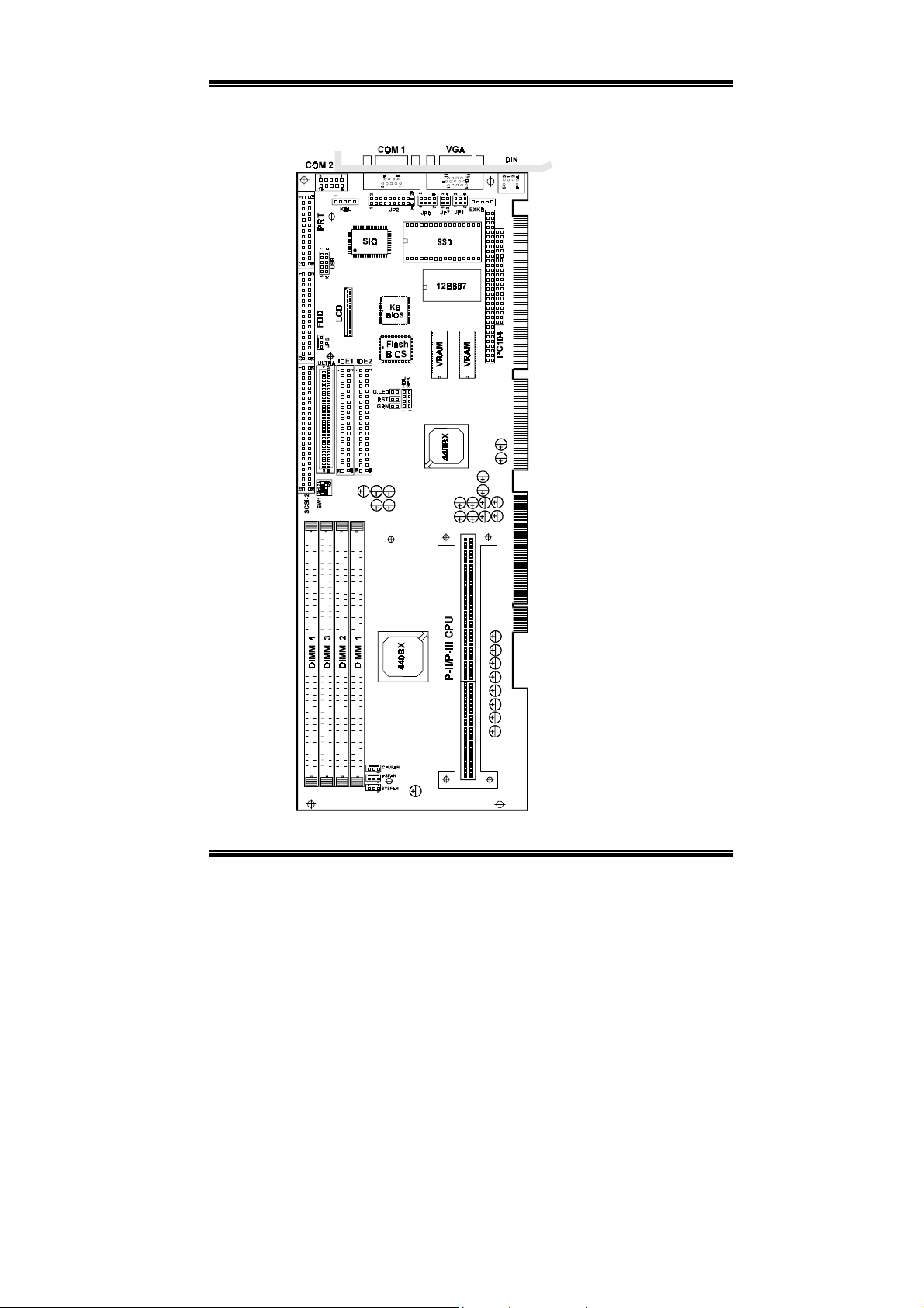
2-2 COMPONENT LOCATIONS
Chapter 2 Hardware Configuration
PC-680 Connector, Jumper and Component locations
PC-680 USER’S MANUAL
Page: 2-3
Page 15
Chapter 2 Hardware Configuration
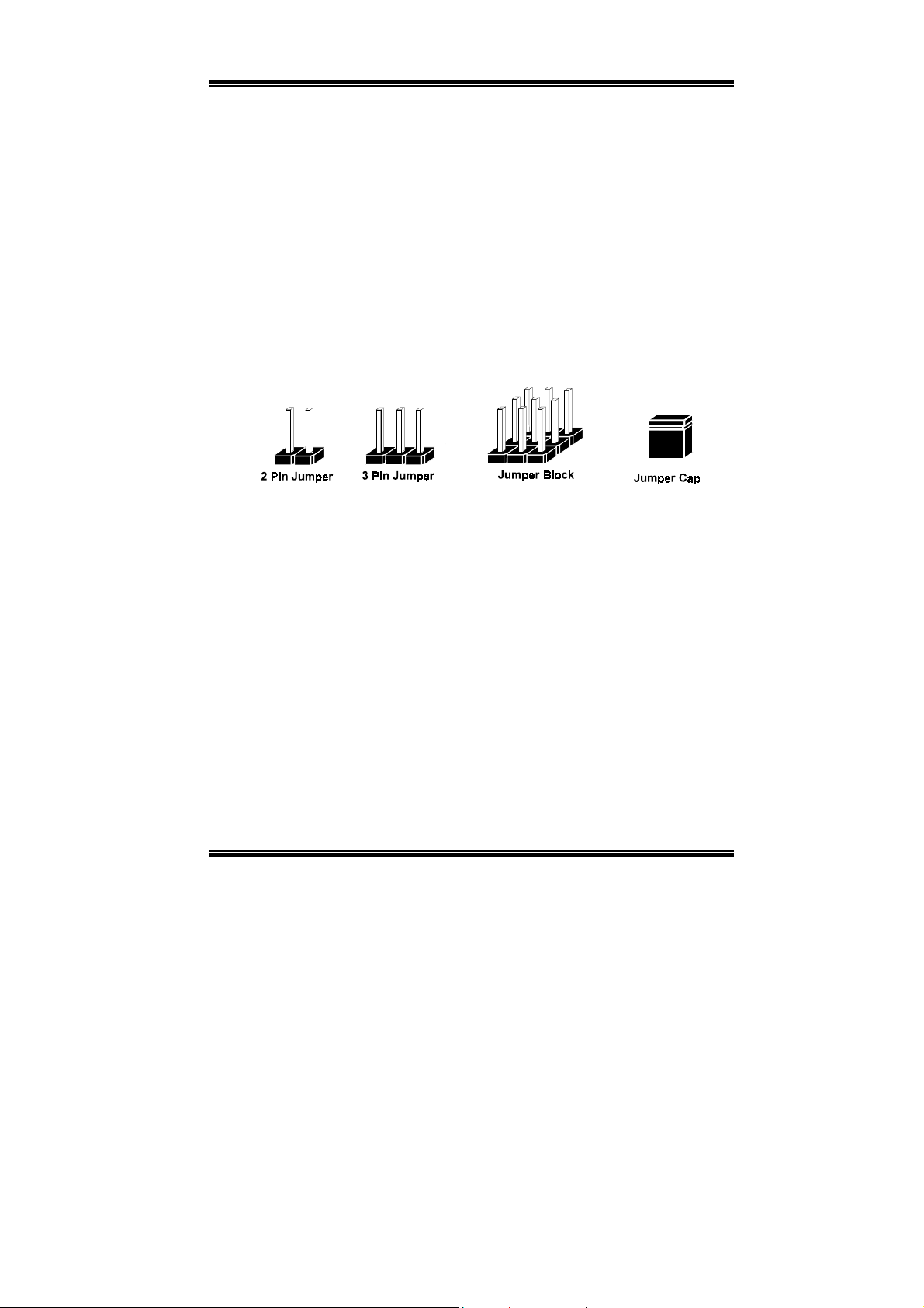
2-3 HOW TO SET THE JUMPERS
You can configure your board by setting the jumpers. A jumper consists of
two or three metal pins with a plastic base mounted on the card, and a
small plastic "cap"( with a metal contact inside) to connect the pins. So you
can set up your har dware configurati on by "opening" or "closing" the pins.
The jumper can be combined into sets which called jumper blocks. When
the jumpers are all in the block, you have to put them together to set up the
hardware configuration. The figure below shows how this loo ks.
JUMPERS AND CAPS
For example, if a jumper has three pins, labelled PIN1, PIN2, and PIN3.
You can connect PIN1 & PIN2 to create one setting and shorting. You can
either connect PIN2 & PIN3 to create another setting. The same jumper
diagrams are applied all t hrough this manual. The figure belo w shows what
the manual diagrams look and what they represent.
Page: 2-4
PC-680 USER
’
S MANUAL
Page 16

JUMPER DIAGRAMS
Chapter 2 Hardware Configuration
JUMPER SETTINGS
PC-680 USER’S MANUAL
Page: 2-5
Page 17

Chapter 2 Hardware Configuration
2-4 CPU TYPE & CLOCK SELECTION
CPU type and Bus Ratio Selection
SW1 :
SW1A5:
The jumper settings are as follows :
2-4-1 Intel P-II 233/266/300/333 CPU type & clock Jumper settings
Intel
P-II
233Mhz
Intel
P-II
266Mhz
Intel
P-II
300Mhz
Intel
P-II
333Mhz
*** Manufactory default -- Intel P-II 266Mhz
CPU Clock Selection
CPU
TYPE
CPU
CLOCK
66Mhz
66Mhz
66Mhz
66Mhz
Jumper Settings
A1 A2 A3 A4 A5
ON
ON
ON
ON
OFF
ON
OFF
ON
SW1
OFF
ON
ON
OFF
ON
OFF
OFF
OFF
ON
ON
ON
ON
ILLUSTRATION
JUMPER
Page: 2-6
PC-680 USER
’
S MANUAL
Page 18

Chapter 2 Hardware Configuration
2-4-2 Intel P-II 350/400/450 CPU type & clock Jumper settings
CPU
TYPE
Intel
P-II
350Mhz
Intel
P-II
400Mhz
Intel
P-II
450Mhz
CPU
CLOCK
100Mhz
100Mhz
100Mhz
Jumper Settings
A1 A2 A3 A4 A5
ON
ON
ON
OFF
ON
OFF
SW1
OFF
ON
ON
ON
OFF
OFF
OFF
OFF
OFF
JUMPER
ILLUSTRATION
PC-680 USER’S MANUAL
Page: 2-7
Page 19

Chapter 2 Hardware Configuration
2-4-3 Intel P-III 450/500/550/600 CPU type & clock Jumper settings
CPU
TYPE
Intel
P-III
450Mhz
Intel
P-III
500Mhz
Intel
P-III
550Mhz
Intel
P-III
600Mhz
CPU
CLOCK
100Mhz
100Mhz
100Mhz
100Mhz
Jumper Settings
A1 A2 A3 A4 A5
ON
ON
ON
OFF
OFF
ON
OFF
ON
SW1
ON
OFF
OFF
ON
OFF
OFF
OFF
ON
OFF
OFF
OFF
OFF
ILLUSTRATION
JUMPER
Page: 2-8
PC-680 USER
’
S MANUAL
Page 20

Chapter 2 Hardware Configuration
2-4-4 Intel P-III 650/700/750/800 CPU type & clock Jumper settings
CPU
TYPE
Intel
P-III
650Mhz
Intel
P-III
700Mhz
Intel
P-III
750Mhz
Intel
P-III
800Mhz
CPU
CLOCK
100Mhz
100Mhz
100Mhz
100Mhz
Jumper Settings
A1 A2 A3 A4 A5
OFF
OFF
OFF
OFF
OFF
ON
OFF
ON
SW1
ON
OFF
OFF
ON
ON
ON
ON
OFF
OFF
OFF
OFF
OFF
ILLUSTRATION
JUMPER
PC-680 USER’S MANUAL
Page: 2-9
Page 21

Chapter 2 Hardware Configuration
2-5 RS232/422/485 (COM2) SELECTION
RS-232/422/485 Selection
JP2 :
COM1 is fixed for RS-232 function only.
COM2 is selectable for RS-232, 422, 485 function.
The jumper settings are as follows :
COM 2
Function
Jumper
settings
(pins closed)
Jumper
illustration
RS-232
Open
RS-422
1-2
5-6
7-8
9-10
11-12
13-14
15-16
17-18
19-20
RS-485
1-3
4-6
7-8
9-10
11-12
13-14
15-16
17-18
19-20
*** Manufactory default --- RS-232.
Page: 2-10
PC-680 USER
’
S MANUAL
Page 22

Chapter 2 Hardware Configuration
2-6 SSD MEMORY MAPPING SELECTION
JP6, JP7 :
A 32-pin SSD socket supports Disk-on-Chip up to 144MB. This PnP Flash
ROM SSD can be installed as one of user‘s hard disk drive. And if set as
Drive C, it can be used to boot up the computer with MS-DOS installed.
The SSD Memory Mapping is as follows:
SSD Memory Map
CC000h-CDFFFh
D0000h-D1FFFh
D4000h-D5FFFh
D8000h-D9FFFh
DC000h-DDFFFh
SSD Memory Mapping Selection
JUMPER SETTINGS
(pins closed)
JP6 JP7
1-2
3-4
3-4
1-2
3-4
3-4
5-6
1-2
5-6
3-4
JUMPER
ILLUSTRATION
E0000h-E1FFFh
*** Manufactory default --- CC000h-CDFFFh
PC-680 USER’S MANUAL
7-8
1-2
Page: 2-11
Page 23

Chapter 2 Hardware Configuration
2-7 AT KEYBOARD / PS2 MOUSE SELECTION
AT Keyboard / PS2 Mouse Selection
JP1 :
The jumper settings are as follows:
AT KEYBOARD
DEVICE
TYPE
JUMPER SETTINGS
(pins closed)
JP1
3-5
4-6
JUMPER
ILLUSTRATION
PS/2 MOUSE
1-3
2-4
*** Manufactory default -- AT Keyboard
2-8 COM1 CONNECTOR
COM1 :
The COM1 Connector assignments are as follows :
COM1 Connector, DB9 male connector
PIN ASSIGNMENT
1 DCD
2 RX
3 TX
4 DTR
5 GND
6 DSR
7 RTS
8 CTS
9 RI
Page: 2-12
PC-680 USER
’
S MANUAL
Page 24

Chapter 2 Hardware Configuration
2-9 COM2 CONNECTOR
COM2 :
COM2 Connector
The COM2 Connector assignments are as follows :
PIN ASSIGNMENT
RS-232 RS-422 RS-485
1 DCD TX- TX2 RX TX+ TX+
3 TX RX+ RX+
4 DTR RX- RX5 GND GND GND
6 DSR RTS- NC
7 RTS RTS+ NC
8 CTS CTS+ NC
9 RI CTS- NC
10 NC NC NC
2-10 KEYBOARD OR PS/2 MOUSE CONNECTOR
Keyboard or PS/2 Mouse Connector
DIN :
The pin assignments are as follows :
PIN
ASSIGNMENT
1 KBDATA MSDATA
2 NC NC
3 GND GND
4 VCC VCC
5 KBCLK MSCLK
6 NC NC
Note: To select keyboard or mouse, user should set the right device
type described on JP1.
PC-680 USER’S MANUAL
Page: 2-13
Page 25

Chapter 2 Hardware Configuration
2-11 EXTERNAL KEYBOARD CONNECTOR
EXKB :
External Keyboard Connector
The pin assignments are as follows :
PIN ASSIGNMENT
1 KBCLK
2 KBDATA
3 NC
4 GND
5 Vcc
2-12 RESET CONNECTOR
Reset Connector.
RST :
The pin assignments are as follows :
PIN ASSIGNMENT
1 Reset
2 Ground
2-13 CPU FAN CONNECTOR
CPUFAN :
The pin assignments are as follows:
PIN ASSIGNMENT
1 GND
2 +12V
3 CPUFAN
CPU Fan connector
Page: 2-14
PC-680 USER
’
S MANUAL
Page 26

Chapter 2 Hardware Configuration
2-14 FLOPPY DISK DRIVE CONNECTOR
Floppy Disk Drive Connector
FDD :
You can use a 34-pin daisy-chain cable to connect two-FDDs. On one end
of this cable is a 34-pin flat cable attach to the FDD connector on the board,
and the other side is attaches to two FDDs.
The pin assignments are as follows :
PIN ASSIGNMENT PIN ASSIGNMENT
1 GND 2 RPM
3 GND 4 NC
5 GND 6 NC
7 GND 8 INDEX
9 GND 10 MTR0
11 GND 12 DRV1
13 GND 14 DRV0
15 GND 16 MTR1
17 GND 18 DIR
19 GND 20 STEP
21 GND 22 WDATA
23 GND 24 WGATE
25 GND 26 TRK0
27 GND 28 WRPRT
29 GND 30 RDATA
31 GND 32 SEL
33 GND 34 DSKCHG
PC-680 USER’S MANUAL
Page: 2-15
Page 27

Chapter 2 Hardware Configuration
2-15 HARD DISK DRIVE CONNECTOR
Hard Disk Drive Connector
IDE1:
The PC-680 possesses two HDD connectors, IDE1 and IDE2. The pin
assignments are as follows:
PIN ASSIGNMENT PIN ASSIGNMENT
1 IDERST 21 IDEREQ0
2 GND 22 GND
3 IDED7 23 IDEIOW
4 IDED8 24 GND
5 IDED6 25 IDEIOR
6 IDED9 26 GND
7 IDED5 27 IDERDY
8 IDED10 28 PULL HI
9 IDED4 29 IDEACK0
10 IDED11 30 GND
11 IDED3 31 IRQ14
12 IDED12 32 IOCS16
13 IDED2 33 IDEA1
14 IDED13 34 GND
15 IDED1 35 IDEA0
16 IDED14 36 IDEA2
17 IDED0 37 IDECS1P
18 IDED15 38 IDECS3P
19 GND 39 IDELEDP
20 N.C. 40 GND
Page: 2-16
PC-680 USER
’
S MANUAL
Page 28

Hard Disk Drive Connector
IDE2:
The pin assignments are as follows:
PIN ASSIGNMENT PIN ASSIGNMENT
1 IDERST 21 IDEREQ1
2 GND 22 GND
3 IDED7 23 IDEIOW
4 IDED8 24 GND
5 IDED6 25 IDEIOR
6 IDED9 26 GND
7 IDED5 27 IDERDY
8 IDED10 28 PULL HI
9 IDED4 29 IDEACK1
10 IDED11 30 GND
11 IDED3 31 IDESIRQ
12 IDED12 32 IOCS16
13 IDED2 33 IDEA1
14 IDED13 34 GND
15 IDED1 35 IDEA0
16 IDED14 36 IDEA2
17 IDED0 37 IDECS1S
18 IDED15 38 IDECS3S
19 GND 39 IDELEDS
20 N.C. 40 GND
Chapter 2 Hardware Configuration
PC-680 USER’S MANUAL
Page: 2-17
Page 29
Chapter 2 Hardware Configuration
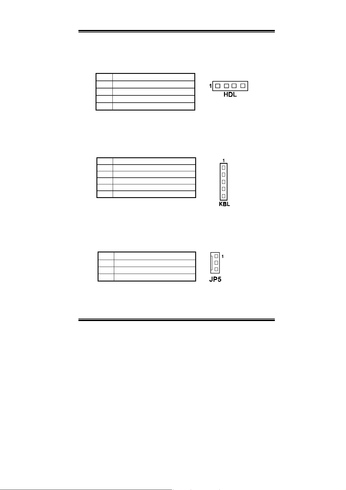
2-16 HARD DISK DRIVE LED CONNECTOR
Hard Disk Drive LED Connector
HDL :
The pin assignments are as follows :
PIN ASSIGNMENT
1 Vcc
2 HDD Active Signal
3 HDD Active Signal
4 HDD Active Signal
2-17 POWER LED & KEYLOCK CONNECTOR
Power LED & Keylock Connector
KBL :
The pin assignments are as follows :
PIN ASSIGNMENT
1 Power LED
2 NC
3 Ground
4 Keyboard INT
5 Ground
2-18 PANEL INVERTER DELAY-POWER CONNECTOR
Panel Invert er Delay-power Conne ctor
JP5 :
This Connector acts as an inverter to supply proper power to LCD panel.
The pin assignments are as follows :
1 LCD +12V
2 GND
3 LCD VDD(+5V)
Page: 2-18
PC-680 USER
’
S MANUAL
Page 30

Chapter 2 Hardware Configuration
2-19 LCD PANEL CONNECTOR
: LCD Panel Connector
LCD
The connector LCD is a 41-pin, dual-in-line header used for Flat Panel
displays.
The pin assignments are as follows :
PIN ASSIGNMENT PIN ASSIGNMENT
1 P20 2 GND
3 P16 4 Vcc
5 P21 6 P0
7 P17 8 P8
9 P22 10 P1
11 P18 12 P9
13 P23 14 P2
15 P19 16 P10
17 Vcc 18 P3
19 FLM 20 P11
21 MDE 22 P4
23 LP 24 P12
25 SHFCLK 26 P5
27 3.3V 28 P13
29 3.3V 30 P6
31 ENABKL 32 P14
33 LCDVDD 34 P7
35 ENVEE 36 P15
37 GND 38 LCD+12V
39 GND 40 LCD+12V
41 NC
PC-680 USER’S MANUAL
Page: 2-19
Page 31
Chapter 2 Hardware Configuration
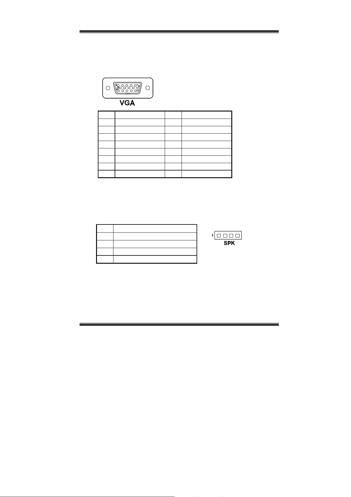
2-20 VGA CRT CONNECTOR
VGA CRT Connector
VGA :
The pin assignments are as follows:
PIN ASSIGNMENT PIN ASSIGNMENT
1 RED 9 NC
2 GREEN 10 GND
3 BLUE 11 NC
4 NC 12 NC
5 GND 13 HSYNC
6 GND 14 VSYNC
7 GND 15 NC
8 GND
2-21 EXTERNAL SPEAKER CONNECTOR
External Speaker Connector
SPK :
The pin assignments are as follows :
1 Vcc
2 Speaker Signal
3 Speaker Signal
4 Speaker Signal
Page: 2-20
PC-680 USER
’
S MANUAL
Page 32

Chapter 2 Hardware Configuration
2-22 PRINTER CONNECTOR
Printer Connector
PRT :
As to link the Printer to the card, you need a cable to connect both DB25
connector and parallel port. The pin assignments are as follows :
PIN ASSIGNMENT PIN ASSIGNMENT
1 STB 14 AUTFE
2 P0 15 ERROR
3 P1 16 INIT
4 P2 17 SLCTIN
5 P3 18 GND
6 P4 19 GND
7 P5 20 GND
8 P6 21 GND
9 P7 22 GND
10 ACK 23 GND
11 BUSY 24 GND
12 PE 25 GND
13 SLCT 26 NC
2-23 POWER SUPPLY FAN CONNECTOR
PSFAN :
The pin assignments are as follows:
PIN ASSIGNMENT
Power Supply Fan connector
1 GND
2 +12V
3 PSFAN
PC-680 USER’S MANUAL
Page: 2-21
Page 33

Chapter 2 Hardware Configuration
2-24 SCSI CONNECTOR
SCSI II Connector
SCSI:
ULTRA:
Ultra wide SCSI Connector
The PC-680 equips with two SCSI Connectors on board, SCSI and
ULTRA. The SCSI is a 50 pins dual-in-line header, ULTRA is a 68 pins
dual-in-line header.The pin assignments are as follows :
PIN ASSIGNMENT PIN ASSIGNMENT PIN ASSIGNMENT
1 GND 18 GND 35 GND
2 GND 19 GND 36 GND
3 GND 20 GND 37 GND
4 GND 21 GND 38 TRMPWR
5 GND 22 GND 39 GND
6 GND 23 GND 40 GND
7 GND 24 GND 41 SATTN8 GND 25 GND 42 GND
9 GND 26 SCD0 43 SBSY10 GND 27 SCD1 44 SACK11 GND 28 SCD2 45 SRST12 GND 29 SCD3 46 SMSG13 GND 30 SCD4 47 SSEL14 GND 31 SCD5 48 SCD15 GND 32 SCD6 49 SREQ16 GND 33 SCD7 50 SIO17 GND 34 SCDPL
Page: 2-22
PC-680 USER
’
S MANUAL
Page 34

ULTRA :
The pin assignments are as follows:
SCSI Connector for Ultra wide SCSI HDD.
Chapter 2 Hardware Configuration
PIN ASSIGNMENT PIN ASSIGNMENT PIN ASSIGNMENT
1 GND 24 GND 47 SCD7
2 GND 25 GND 48 SCDPL
3 GND 26 GND 49 GND
4 GND 27 GND 50 GND
5 GND 28 GND 51 TRMPWR
6 GND 29 GND 52 TRMPWR
7 GND 30 GND 53 NC
8 GND 31 GND 54 GND
9 GND 32 GND 55 SATTN10 GND 33 GND 56 GND
11 GND 34 GND 57 SBSY12 GND 35 SCD12 58 SACK13 GND 36 SCD13 59 SRST14 GND 37 SCD14 60 SMSG15 GND 38 SCD15 61 SSEL16 GND 39 SCDPH 62 SCD17 GND 40 SCD0 63 SREQ18 GND 41 SCD1 64 SIO19 NC 42 SCD2 65 SCD8
20 GND 43 SCD3 66 SCD9
21 GND 44 SCD4 67 SCD10
22 GND 45 SCD5 68 SCD11
23 GND 46 SCD6
0The SCSI function of this CPU Card is designed based on PCI Bus
Master, that means that one of th e PCI Bus Master is occupied. (The
SCSI Bus Master (DRQ3) is same as 4th PCI Slot on the backplane
(DRQ3).
backplane would fail even if SCSI function is di sabled.
When the SCSI chipset is on-board, the 4th PCI slot on
PC-680 USER’S MANUAL
Page: 2-23
Page 35

Chapter 2 Hardware Configuration
2-25. SYSTEM FAN CONNECTOR
SYSFAN :
System Fan Connector
The pin assignments are as follows:
PIN ASSIGNMENT
1 GND
2 +12V
3 SYSFAN
2-26. GREEN FUNCTION CONNECTOR
Green Function Co nnector
GRN:
The pin assignments are as follows:
PIN ASSIGNMENT
1 EXTSMI2 GND
2-27. UNIVERSAL SERIAL BUS CONNECTOR
Universal Serial Bus Connector
USB:
The pin assignments are as follows:
PIN ASSIGNMENT
1 VCC
2
3
4 GND
5 GND
6 VCC
7
8 USBP1+
9 GND
10 GND
USBP∅−
USBP∅+
USBP1−
Page: 2-24
PC-680 USER
’
S MANUAL
Page 36

Chapter 2 Hardware Configuration
2-28. SOLID-STATE DISK SOCKET
SSD: 32pin Solid State Disk Socket
The pin assignments are as follows:
PIN ASSIGNMENT PIN ASSIGNMENT
1 NC 17 SD3
2 NC 18 SD4
3 NC 19 SD5
4 SA12 20 SD6
5 SA7 21 SD7
6 SA6 22 CE
7 SA5 23 SA10
8 SA4 24 OE
9 SA3 25 SA11
10 SA2 26 SA9
11 SA1 27 SA8
12 SA0 28 NC
13 SD0 29 NC
14 SD1 30 VCC
15 SD2 31 WE
16 GND 32 VCC
PC-680 USER’S MANUAL
Page: 2-25
Page 37

Chapter 2 Hardware Configuration
2-29. MEMORY INSTALLATION
The PC-680 P-II/P-III Embedded Computer can support 4 SDRAM banks.
Note:
(168pin x 32bit x 4)
DRAM BANK CONFIGURATION
DIMM 1 DIMM 2 DIMM 3 DIMM 4 TOTAL MEMORY
DIMM 1,2,3,4 for double Bank SDRAM module
32M 32M
32M 32M 64M
32M 32M 32M 96M
32M 32M 32M 32M 128M
32M 64M 96M
32M 64M 32M 128M
32M 64M 64M 64M 224M
32M 64M 128M 64M 288M
32M 128M 128M 64M 352M
64M 64M
64M 64M 128M
64M 64M 64M 192M
64M 32M 32M 64M 192M
64M 64M 64M 64M 256M
64M 32M 64M 64M 224M
64M 128M 192M
64M 128M 128M 320M
64M 64M 64M 128M 320M
64M 32M 64M 128M 288M
64M 128M 128M 128M 448M
128M 128M
128M 128M 256M
128M 32M 64M 128M 352M
128M 64M 128M 320M
128M 128M 128M 384M
128M 128M 128M 32M 416M
128M 64M 128M 128M 448M
128M 128M 128M 128M 512M
Page: 2-26
PC-680 USER
’
S MANUAL
Page 38

SOFTWARE
CHAPTER
3
UTILITIES
This chapter comprises the detailed information of VGA driver, SCSI
driver, and BIOS update. It also describes how to configure the
Watchdog Timer.
Section includes:
z VGA Driver Utilities
z Flash BIOS Update
z SCSI Driver Utilities
z Watchdog Timer Configuration
Page: 3-1
Page 39

Chapter 3 Software Configuration
3-1. INTRODUCTION
Enclosed with our PC-680 package is our driver utility, which may comes
in a form of a CD ROM disc or floppy diskettes. For CD ROM disc user,
you will only need some of the files contained in the CD ROM disc, please
kindly refer to the following chart:
File name
(Assume that CD ROM drive is D:)
D:\VGA\C&T\CT6555x For VGA driver installation
D:\Flash\Awdflash.exe For BIOS update
D:\SCSI\AIC7880 For SCSI driver installation
3-2. VGA DRIVER UTILITY
The VGA interface embedded with our PC-680 can support a wide range
of display mode, such as SVGA, STN, TFT, EL,.....etc. You can display
CRT and LCD Panel simultaneously on this board, but make sure that the
modes for CRT and LCD Panel are the same. If not, only one of them
can be displayed.
Purpose
Page:3-2
′
PC-680 USER
S MANUAL
Page 40

3-2-1. Installation of VGA Driver for PCI
1. Install VGA Driver to Windows 3.1
(1). To install VGA driver to Windows 3.1, please insert Utility
Disk into floppy disk drive A/B or CD ROM drive under
your Windows 3.1 system, and go to directory where VGA
driver is located.
(2). Click Setup.exe file for VGA driver installation directly.
Follow the instructions on the screen and complete the
installation.
(3). Once installation is completed, you must shut down system
and restart in order for changes to take effect.
2. Install VGA Driver to Windows 95
(1). Click START, SETTINGS, then CONTROL PANEL.
(2). On CONTROL PANEL, click the DISPLAY icon and enter
the SETTINGS tab of the DISPLAY PROPERTIES
window.
(3). Select the SETTINGS page, push the CHANGE DISPLAY
TYPE button. Click the CHANGE button in the “Adaper
Type” area.
(4). Push the “HAVE DISK BUTTON” and press OK.
(5). Specify the path for the new driver and press the <Enter>
key. The “Select Device” dialog box will appear. Select
the “Chips and Tech 65550 PCI”.
(6). Follow the remaining instructions that appear on the screen
to complete the rest of the installation, and then restart your
computer.
3. Install VGA driver to Windows NT 3.5x/4.0
(1). To install VGA drivers to Windows 3.5x/4.0 is as you
normally would. Click START, then SETTINGS, then
CONTROL PANEL of the operating system.
(2). Select the DISPLAY icon to start the DISPLAY
PROPERTIES window, then choose the SETTING tab,
then DISPLAY TYPE.
(3). In the CHANGE DISPLAY TYPE window, click on the
CHANGE button in the ADAPTER TYPE, this will bring
up the SELECT DEVICE window.
Chapter 3 Software Configuration
PC-680 USER′S MANUAL
Page:3-3
Page 41

Chapter 3 Software Configuration
(4). In the CHANGE DISPLAY window, click on Have Disk.
Follow the instructions appearing on the screen until you
complete the whole installation.
(5). Once installation is completed, the system must be shut
down and restarted for the new drivers to take effect.
4. Install VGA driver to OS/2 Warp Operation System
(1) Preliminary Steps:
(i) OS/2 DOS Support must be installed.
(ii) If you previously installed SVGA support, you must reset
the system to VGA mode. VGA is the default video mode
enable when OS/2 is to be installed.
(iii) To resto re VGA mode, Use SELECTIVE INSTALL and
select VGA for PRIMARY DISPLAY. For more
information on this procedure, see the section on
Changing Display Adapter Support in the OS/2 User’s
Guide.
(2) Start Driver installation
(i) Open an OS/2 full screen or windowed session.
(ii) Place into Drive A/B the Utility Disk, which contains the
65550 Display Driver.
(iii) At the OS/2 command prompt , type the following
commands to copy the files to the OS/2 drive:
T ype A: and press ENT E R to make this the default drive.
Type Setup A: C: and press ENTER
When the setup Program is completed, you will need to
perform a shut down and then restart the system in order for
changes to take effect.
(iv) After restarting the system, first open the OS/2 System
folder.
(v) Then open the System Setup folder.
(vi) Open the Display Driver Install Object.
(vii) When the Display Driver Install window appears, select
PRIMARY DISPLAY, and click OK.
(viii) When the Primary Display Driver List window appears,
select “Chips and Technologies 65550” from the list of
Adapter types, then select OK to install the video driver.
Page:3-4
′
PC-680 USER
S MANUAL
Page 42

Chapter 3 Software Configuration
(ix) When installation is complete, you should shut down and
restart the system for the changes to take effect. And also
make sure to remove the install Utility Disk before
restarting system.
3-3. FLASH BIOS UPDATE
3-3-1. System BIOS Update:
Users of PC-680 can use the program “Awdflash.exe” contained in
the Utility Disk for system BIOS and VGA BIOS update.
3-3-2. To update VGA BIOS for LCD Flat Panel Display:
As PC-680 user, you have to update the VGA BIOS for your specific
LCD flat panel you are going to use. For doing this, you need two
files. One is the “Awdflash.exe” file and the other is the VGA BIOS
C&T 65550 file for LCD panel display. Both file must be provided by
the vendor or manufacturer. When you get these two files ready,
follow the following steps for updating your VGA BIOS:
1. Install “Awdflash.exe” from Utility Disk to Drive C.
2. Insert the VGA BIOS file you have obtained from the vendor.
3. Type the path to Awdflash.exe and execute the VGA BIOS update
with file 680xxxxx.bin
C:\UTIL\AWDFLASH>AWDFLASH 680xxxxx.bin
4. The screen will display the table below:
FLASH MEMORY WRITER v7.XX
(C) Award Software 1999 All Rights Reserved
For i440BX-SMC669-2A69KP69C-0 DATE: 12/12/1999
Error Messa ge : Do You W ant To Save BIOS (Y/N)
If you want to save up the original BIOS, enter "Y" and press < Enter
> . If you choose "N", the following table will appear on screen.
PC-680 USER′S MANUAL
Flash Type: MXIC 28F2000PPC/12V
File Name to Program: 680xxxxx.bin
Checksum: XXXXX
Page:3-5
Page 43

Chapter 3 Software Configuration
FLASH MEMORY WRITER v7.XX
(C) Award Software 1999 All Rights Reserved
For i440BX-SMC669-2A69KP69C-0 DATE: 12/12/1999
Flash Type: MXIC 28F2000PPC/12V
File Name to Program: F60xxxxx.bin
Checksum: XXXXX
Error Message : Are You Sure To Program (Y/N)
Select "Y", and the BIOS will be renewed. When you are refreshing
the BIOS, do not turn off or reset the system, or you will damage the
BIOS. After you have completed all the programming, the screen
displays the table below:
FLASH MEMORY WRITER v7.XX
(C) Award Software 1999 All Rights Reserved
For i440BX-SMC669-2A69KP69C-0 DATE: 12/12/1999
Flash Type: MXIC 28F2000PPC/12V
File Name to Program: F60xxxxx.bin
Checksum: XXXXX
Page:3-6
Reset System or Power off to
F1: Reset F10: Exit
accomplish update process!
Please reset or power off the system, and then the Flash BIOS is fully
implemented.
′
PC-680 USER
S MANUAL
Page 44

3-4. SCSI DRIVER UTILITY
3-4-1. Introduction
PC-680 is embedded with SCSI Adaptec 7880 can support SCSI II
and Ultra-wide SCSI. Installation programs are provided as follows:
Chapter 3 Software Configuration
Details on Installation procedure is found in the README.TXT
file found on SCSI DRIVER UTILITY.
PC-680 USER′S MANUAL
Page:3-7
Page 45

Chapter 3 Software Configuration
3-5. WATCHDOG TIMER CONFIGURATION
The watchdog timer can reset the system automatically. It is defined at I/O
port
port
function, write I/O port
the Watchdog function.
The PC-680 watchdog function, You must write your program so when it
writes I/O port address 0443 for enable watchdog and write I/O port
address 0441 for disable watchdog. The timer's intervals have a tolerance of
25% so you should program an instruction that will refresh the timer about
every second.
The following program shows you how to program the watch timer in your
program.
Watchdog enable program:
MOV AX, 000FH (choose the values you need; start from 0)
MOV DX, 0443H
OUT DX, AX
Watchdog disable program:
MOV AX, 000FH (this value can be ignored)
MOV DX, 0441H
OUT DX, AX
The Watchdog Timer control table is as follow:
Level Value Time/sec Level Value Time/sec
. When you want to enable the watchdog timer, please write I/O
0443H
, then the system will reset itself. When you want to disable the
0443H
, the system will run the command to stop
0441H
1 F 0 9 7 64
2 E 8 10 6 72
3 D 16 11 5 80
4 C 24 12 4 88
5 B 32 13 3 96
6 A 40 14 2 104
7 9 48 15 1 112
8 8 56 16 0 120
Page:3-8
′
PC-680 USER
S MANUAL
Page 46

CHAPTER
GREEN PC
FUNCTION
This chapter gives you the concise information for Green PC Function.
Section includes:
! Power Saving Block Diagram
! CPU Doze Mode
! System STANDBY Mode
! System SUSPEND Mode
4
Page: 4-1
Page 47

Chapter 4 Green PC Function
4-1. POWER SAVING BLOCK DIAGRAM
4-2. CPU DOZE MODE
1. After timing out, CPU clock slows down to 8MHz.
2. Flash LED to indicate power saving status.
3. Monitor Activity, according to the setting of Advanced Setup.
4. Any activity occurs, system will exit from Doze mode to On mode.
4-3. SYSTEM STANDBY MODE
1. After timing out, CPU clock slows down to 8MHz.
2. Flash LED to indicate power saving status.
3. Level 1 cache are disabled.
4. VGA monitor displays blank screen.
5. Fixed disk driver motor will be spin off.
6. Any activity occurs, system will exit from Standby mode to On mode.
Page: 4-2
PC-680 USER
′
S MANUAL
Page 48

Chapter 4 Green PC Function
4-4 SYSTEM SUSPEND MODE
1. After timing out, CPU clock is slow down to 8MHz, if you use Intel
Pentium or Cyrix (SMI) CPU, then CPU clock will be stopped.
2. Three 3 beep sounds.
3. Flash LED to indicate power saving status.
4. Level 2 cache are disabled.
5. VGA monitor displays blank screen.
6. Fixed disk driver motor will be spin off.
7. Monitor activity according to the setting of Advanced Setup.
8. When system in Suspend mode, only Keyboard / Mouse / Alarm resume
can wakeup system.
PC-680 USER′S MANUAL
Page: 4-3
Page 49

Chapter 4 Green PC Function
Page: 4-4
′
PC-680 USER
S MANUAL
Page 50

AWARD
BIOS SETUP
This chapter states out how to set up the Award BIOS.
This section includes:
! Introduction
! Entering Setup
! The Standard CMOS Setup
! The BIOS Features Setup
! The Chipset Features Setup
! Power Management Setup
! PNP/PCI Configuration
! Load BIOS defaults
! Integrated Peripherals
! IDE HDD Auto Detection
! Save Setup and Exit Setup
CHAPTER
5
Page: 5-1
Page 51

Chapter 5 Award BIOS Setup
5-1. INTRODUCTION
This chapter will show you the function of a BIOS in managing the
features of your system. The PC-680 P-II/P-III Embedded Card is
equipped with the BIOS for system chipset from Award Software Inc. This
page briefl y explains the function of a BIOS in managing t he special
features of your system. T he following pages de scribe how to use the
BIOS for system chipset Setup menu.
Your application programs (such as word processing, spreadsheets, and
games) rely on an operating system such as DOS or OS/2 to manage such
things as keyboard, monitor, disk drives, and memory.
The operating system relies on a BIOS (Basic Input and Output system), a
program stored on a ROM (Read-only Memory) chip, to initialize and
configure your computer's hardware. As the interface between the
hardware and the operating system, the BIOS enables you to make basic
changes to your system's hardware without having to write a new operating
system.
The following diagram illustrates the interlocking relationships between the
system hardware, BIOS, operating system, and application program:
Page: 5-2
′
PC-680 USER
S MANUAL
Page 52

Chapter 5 Award BIOS Setup
5-2 ENTERING SETUP
When the system is powered on, the BIOS will enter the Power-On Self
Test (POST) routines and the following message will appear on the lower
screen.
As long as this message is present on the screen you may press the <Del>
key (the one that shares the decimal point at bottom of the number keypad)
to access the Setup program. In a moment, the main menu of the Award
SETUP program will appear on the screen:
You may use the cursor up/down keys to highlight the individual menu
items. As you highlight each item, a brief description of that item's function
appears in the lower window. If you have a color monitor you can use the
Shift F2 keys to scroll through the various co l or combinations available.
PC-680 USER′S MANUAL
PRESS <DEL> TO ENTER SETUP, ESC TO SKIP MEMORY TEST
ROM / PCI / ISA BIOS (2A69KP69)
CMOS SETUP UTILITY
AWARD SOFT WARE, INC.
STANDARD CMOS SETUP
BIOS FEATURES SETUP
CHIPSET FEATURES SETUP
POWER MANAGEMENT SETUP
PNP/PCI CINFIGURATION
LOAD BIOS DEFAULTS
INTEGRATED PERI PHERALS
SUPERVISOR PASSWORD
USER PASSWORD
IDE HDD AUTO DETECTION
SAVE & EXIT SETUP
EXIT WITHOUT SAVING
LOAD SETUP DEFAULTS
Esc : Quit
↑↓→←
:SELECT ITEM
F10 : Save & Exit Setup (Shift)F2 : Change Color
Time, Date, Hard Disk Type.........
Setup program initial screen
Page: 5-3
Page 53

Chapter 5 Award BIOS Setup
5-3 THE STANDARD CMOS SETUP MENU
Highlight〝STANDARD CMOS SETUP〞and press < ENTER > and the
screen will display the following table:
ROM PCI / ISA BIOS (2A69KP69)
STANDARD CMOS SETUP
AWARD SOFT WARE, INC.
Date (mm:dd:yy) : Tue, Jul 14 1998
Time (hh:mm:ss) : 10 : 19 : 9
Type SIZE
Primary Master : Auto
Primary Slave
Secondary Master : Auto
Secondary Slave
: Auto
: Auto
Drive A : 1.44M , 3.5 in.
Drive B : None
Video : EGA/VGA
Halt On
: All, But keyboard
Esc : Quit
F1 : Help (Shift) F2 : Change Color
In the above table the base memory size and the extended memory size are
displayed. This is automatically read from your systems, and you do not
need to set these parameters. The screen shows a calendar. The week
display will depend on the date set in your system clock and the flashing
indicating the current date. Since you have not yet set the time and date, the
date displayed is probably incorrect. The description on each item are as
follows:
Date:
< Month >, < Date > and <Year >. Ranges for each value are in the CMOS
Setup Screen, and the week-day will skip automatically.
CYLS. HEADS PRECOMP LANDZONE SECTORS MODE
0 0 0
0 0 0
0 0 0
0 0 0
0 0 0 AUTO
0 0 0 AUTO
0 0 0 AUTO
0 0 0 AUTO
Base Memory: 640K
Extended Memory: 1300484K
Other Memory: 384K
----------------------------------Total Memory: 131072K
:Select Item Pu/Pd/+/- : Modify
↑↓→←
CMOS setup screen
Page: 5-4
′
PC-680 USER
S MANUAL
Page 54

Chapter 5 Award BIOS Setup
Time:
< Hour >, < Minute >, and < Second >. Use 24 hour clock format, i.e., for
PM numbers, add 12 to the hour. For examples, 4: 30 P.M. You should
enter the time as 16:30:00.
Primary Master/Primary Slave/Secondary Master/Secondary Slave :
The categories identify the types of 2 channels that have been installed in
the computer. There are 45 predefined types and 4 user definable types are
for Enhanced IDE BIOS. Type 1 to Type 45 are predefined. Type User is
user-definable.
Press PgUp / <+> or PgDn / <-> to select a numbered hard disk type or
type the number and press < Enter >. Note that the specifications of your
drive must match with the drive table. The hard disk will not work
properly if you enter improper information for this category. If your hard
disk drive type is not matched or listed, you can use Type User to define
your own drive type manuall y.
If you select Type User, related information is asked to be entered to the
following items. Enter the information directly from the keyboard and
press < Enter >. This information should be provided in the documentation
from your hard disk vendor or the system manufacturer.
If the controller of HDD interface is ESDI, the selection shall be
"Type 1".
If the controller of HDD interface is SCSI, the selection shall be "None"
If the controller of HDD interface is CD-ROM, the selection shall be
"None"
TYPE:
This is the number designation for a drive with certain identification
parameters.
CYLS.:
This is the number of cylinders found in the specified drive type.
HEADS:
This is the number of heads found in the specified drive type.
PC-680 USER′S MANUAL
Page: 5-5
Page 55

Chapter 5 Award BIOS Setup
PRECOMP:
Precomp is the read delay circuitry which takes into account the timing
differences between the inner and outer edges of the surface of the disk
platter. The number designates the starting cylinder of the signal.
LANDZONE:
Landzone is the landing zone of the heads. This number determines the
cylinder location where the heads will normally park when the system is
shut down.
SIZE (CAPACITY):
This is the formatted capacity of the drive based on the following formula:
(# of heads) X (# of cylinders) X (# of sets) X ( 512bytes/sects)
SECTORS :
This is the number of sectors per track. MFM drives have 17 sectors per
track. RLL drives have 26 sectors per track. ESDI drives have 34 sectors
per track. SCSI and IDE drive may have even more sectors per track.
DRIVE A AND DRIVE B:
The option are 360KB 5.25in, 1.2KB 5.25in, 720KB 3.5in, 1.44MB 3.5in,
2.88MB 3.5in and None. Not Installed could be used as an option for
diskless workstations.
VIDEO:
This category selects the type of video adapter used for the primary
system monitor. Although secondary monitors are supported, you do
not have to select the type in Setup. Available options are EGA/VGA,
CGA 40, CGA 80, and MONO.
HALT ON:
This category allows user to choose whether the computer will stop if an
error is detected during power up. The available options are “All errors”,
“No errors”, “All, But keyboard”, “All, But Diskette”, and “All But
Disk/Key”.
Page: 5-6
′
PC-680 USER
S MANUAL
Page 56

HARD DISK ATTRIBUTES:
Type Cylinders Heads V-P comp LZone Sect Capacity
1 306 4 128 305 17 10
2 615 4 300 615 17 20
3 615 6 300 615 17 30
4 940 8 512 940 17 62
5 940 6 512 940 17 46
6 615 4 65535 615 17 20
7 642 8 256 511 17 30
8 733 5 65535 733 17 30
9 900 15 65535 901 17 112
10 820 3 65535 820 17 20
11 855 5 65535 855 17 35
12 855 7 65535 855 17 49
13 306 8 128 319 17 20
14 733 7 65535 733 17 42
15 000 0 0000 000 00 00
16 612 4 0000 663 17 20
17 977 5 300 977 17 40
18 977 7 65535 977 17 56
19 1024 7 512 1023 17 59
20 733 5 300 732 17 30
21 733 7 300 732 17 42
22 733 5 300 733 17 30
23 306 4 0000 336 17 10
24 977 5 65535 976 17 40
25 1024 9 65535 1023 17 76
26 1224 7 65535 1223 17 71
27 1224 11 65535 1223 17 111
28 1224 15 65535 1223 17 152
29 1024 8 65535 1023 17 68
30 1024 11 65535 1023 17 93
31 918 11 65535 1023 17 83
32 925 9 65535 926 17 69
33 1024 10 65535 1023 17 85
34 1024 12 65535 1023 17 102
35 1024 13 65535 1023 17 110
36 1024 14 65535 1023 17 119
37 1024 2 65535 1023 17 17
38 1024 16 65535 1023 17 136
39 918 15 65535 1023 17 114
40 820 6 65535 820 17 40
41 1024 5 65535 1023 17 42
42 1024 5 65535 1023 26 65
43 809 6 65535 852 17 40
44 809 6 65535 852 26 61
45 776 8 65335 775 33 100
47 AUTO
Chapter 5 Award BIOS Setup
Award Hard Disk Type Table
PC-680 USER′S MANUAL
Page: 5-7
Page 57

Chapter 5 Award BIOS Setup
5-4 THE BIOS FEATURES SETUP MENU
Choose the〝BIOS FEATURES SETUP〞in the main menu, the screen
shown as below.
ROM PCI/ISA BIOS (2A69KP69)
BIOS FEATURES SETUP
Virus Warning
CPU Internal Cache
External Cache
CPU L2
Quick Power On Self Test
Boot Sequence
Swap Floppy Drive
Boot Up Floppy Seek
Boot Up Numlock Status
Gate A20 Option
Typematic Rate Setting
Typematic Rate (Chars/Sec)
Typematic Delay (Msec)
Security Option
PCI/VGA Palette snoop
OS Select For DRAM > 64Mb
Report No FDD For WIN 95
Cache
ECC
The BIOS FEATURES SETUP allows you find true certain features
supported by the chipset and Award BIOS. It also includes support for
shadow RAM under which the contents of the ROM BIOS can be copied
into memory at boot up, enhancing performance. When you change any of
the setting, you may recall the default settings at any time from the main
menu.
To get help on each item, highlight the relevant item and press the F1 key.
A Windows will appear on your screen detailing the various options
available for each item.
A brief introduction of each setting in the BIOS FEATURES SETUP
program is given on next page.
AWARD SOFT WARE, INC.
: Disabled
: Enabled
: Enabled
: Enabled
: Disabled
: A,C, SCSI
: Disabled
: Enabled
: On
: Fast
: Disabled
: 6
: 250
: Setup
: Disabled
: Non-OS2
: No
Checking
BIOS Features Setup
Video BIOS Shadow
C8000-CBFFF Shadow
CC000-CFFFF Shadow
D0000-D3FFF Shadow
D4000-D7FFF Shadow
D8000- DBFFF Shadow
DC000-DFFFF Shadow
Esc : Quit
F1 : Help Pu/Pd/+/- : Modify
F5 : Old Values (Shift)F2 : Color
F6 : Load BIOS Defaults
F7 : Load Setup Defaults
↑↓→←
: Enabled
: Disabled
: Disabled
: Disabled
: Disabled
: Disabled
: Disabled
: Select Item
Page: 5-8
′
PC-680 USER
S MANUAL
Page 58

VIRUS WARNING:
When enabled, the BIOS will supervise the boot sector and partition
table of the hard disk drive for any attempt for modification.
CPU INTERNAL CACHE:
This item should always be Enable, If your system has 486CPU or above.
Even if you have installed the external cache. If you have no external cache
installed this item should be enabled to allow use of the internal cache in
the CPU.
EXTERNAL CACHE:
Enable or disable this function according to whether you want external
cache enabled or disabled.
QUICK POWER ON SELF TEST:
You can enable or disable this item to speed up Power On Self Test (POST)
after you power on the computer. If it is set to Enable, BIOS will shorten or
skip some check items during POST.
BOOT SEQUENCE:
You may define whether the system will look first at drive A: and then at
drive C: when boot ing up, or vice versa.
BOOT UP FLOPPY SEEK:
You may enable / disable this item to define whether the system will look
for a floppy disk drive to boot at power-on, or directly to the hard disk
drive.
BOOT UP NUMLOCK STATUS:
Use this item to enable / disable the NumLock on your keyboard
automatically at power-on.
BOOT UP SYSTEM SPEED:
Select High to configure your system in the turbo speed mode at boot up,
select Low to configure your system in normal speed mode. Whichever
setting you choose you will still be able to use the turbo switch to toggle
between the tow modes during use.
Chapter 5 Award BIOS Setup
PC-680 USER′S MANUAL
Page: 5-9
Page 59

Chapter 5 Award BIOS Setup
MEMORY PARITY CHECK:
Enable or Disable this item according to whether you wish the system to
check the memory parity during boot up or not. If you disable this item
even if the BIOS encounters a parity error it will be ignored. We
recommend that you always enable the item in order to ensure that the
memory is good each time you turn your PC on.
GATE 20A OPTION:
When you set this category as Fast. The A20 signal is controlled by chipset
specific method.
TYPEMATIC RATE SETTING:
Enable this item if you wish to be able to configure the characteristics of
your keyboard. Typematic refers to the way in which characters are entered
repeatedly if a key is held down. For example, if you press and hold down
the "A" key, the letter "a" will repeatedly appear on your screen on your
screen until you release the key.
TYPEMATIC RATE (CHARS-SEC):
You can use this item to define the typematic rate delay of your keyboard,
i.e. the rate at which characters will be repeated when a key held down.
TYPEMATIC DELAY (MSEC):
You can use this item to define the period after which the typematic
function become active i.e. how long after you press a key the characters
will be repeated.
SECURITY OPTION:
This category allows you to limit access to the system and Setup, or just to
Setup. To disable security, select PASSWORD SETTING at Main Menu
and then you will be asked to enter password. Do not type anything and just
press <Enter>, it will disable security. Once the security is disabled, the
system will boot and you can enter Setup freely.
Page: 5-10
′
PC-680 USER
S MANUAL
Page 60

5-5 CHIPSET FEATURE SETUP
Choose the〝CHIPSET FEATURES SETUP〞from the main menu, the
screen shown as below.
ROM PCI/ISA BIOS (2A69KP69)
CHIPSET FEATURES SETUP
Auto Configuration
EDO DRAM Speed Selection
EDO CASx# MA Wait State
EDO RASx# Wait State
SDRAM
RAS-to-CAS Delay
SDRAM
RAS Precharge Time
SDRAM CAS latency Time
SDRAM Precharge Control
DRAM Data Integrity Mode
System BIOS Cacheable
Video BIOS Cacheable
Video RAM Cacheable
8 Bit I/O Recovery Time
16 Bit I/O Recovery Time
Memory Hole At 15M-16M
Passive Release
Delayed Transaction
AGP Aperture S ize (M B)
By moving cursor to the desired selection and pressing < F1 > key, the all
options for the desired selection will be displayed for choice. User has to
use select the desired option.
The parameters in this screen are for system designers, service personnel,
and technically competent users only. Do not reset these values unless you
fully understand the consequences of your changes.
AUTO CONFIGURATION FUNCTION:
Auto Configuration selects predetremined optimal values of chipset
parameters. When disabled, chipset parameters revert to setup information
stored in CMOS. Many fields in this screen are not available when Auto
Configuration is Enabled.
AWARD SOFT WARE, INC.
: Enable
: 60 ns
: 2
: 2
: 3
: 3
: 3
: Disabled
Non-ECC
:
: Disabled
: Disabled
: Disabled
: 1
: 1
: Disabled
: Enabled
: Disabled
: 64
Chipset Features Setup
Chapter 5 Award BIOS Setup
Auto Detect DIMM/PCI Clk
Spread Spectrum Modulated
CPU Host Clock
Esc : Quit
F1 : Help Pu/Pd/+/- : Modify
F5 : Old Values (Shift)F2 : Color
F6 : Load BIOS Defaults
F7 : Load Setup Defaults
↑↓→←
: Enabled
: Disabled
: Default
: Select Item
PC-680 USER′S MANUAL
Page: 5-11
Page 61

Chapter 5 Award BIOS Setup
EDO DRAM SPEED SELECTION:
The DRAM timing is controlled by the DRAM Timing Registers. The
timings programmed into this register are dependent on the system design.
Slower rates may be required in certain system designs to support loosse
layouts or slower memory.
EDO CASx# MA WAIT STATE:
You can select the timing control type of EDO DRAM CAS MA. (memory
address bus)
The choice: 1,2.
EDO RASx# WAIT STATE:
You can select the timing control type of EDO DRAM RAS MA (memory
address bus).
SDRAM RAS-to-CAS DELAY:
You can select RAS to CAS Delay time in HCLKs of 2/2 or 3/3. The
system board designer should set the values in this field, depending on the
DRAM installed. Do not change the values in this field unless you change
specifications of the installed DRAM or the installed CPU.
SDRAM RAS PRECHARGE TIME:
Defines the length of time for Row Address Strobe is allowed to precharge.
SDRAM CAS LATENCY TIME:
You can select CAS latency time in HCLKs of 2/2 or 3/3. The system board
designer should set the values in this field, depending on the DRAM
installed. Do not change the values in this filed unless you change
specifications of the installed DRAM or the installed CPU.
DRAM DATA INTEGRITY MODE:
Select parity or ECC (error-correcting code), according to the type of
installed DRAM.
SYSTEM BIOS CACHEABLE :
Select Enabled allows caching of the system BIOS ROM at F000h-FFFFFh,
resulting for a better system performance. However, if any program writes
to this memory area, a system error may result.
Page: 5-12
′
PC-680 USER
S MANUAL
Page 62

VIDEO BIOS CACHEABLE:
Select Enabled allows caching of the video BIOS ROM at C0000h-F7FFFh,
resulting in better video performance. However, if any program writes to
this memory area, a system error may result.
VIDEO RAM CACHEABLE:
Select Enabled allows caching of the video RAM, resulting in better system
performance. However, if any program writes to this memory area, a system
error may result.
8 BIT I/O RECOVERY TIME:
The recovery time is the length of time, measured in CPU clocks, which the
system will delay after the completion of an input/output request. This
delay takes place becaue the CPU is operating so much faster than the
input/output bus that the CPU must be delayed to allow fro the completion
of the I/O. This item allows you to determine the recovery time allowed for
8bit I/O.
16 BIT I/O RECOVERY TIME:
This item allows you to determine the recovery time allowed for 16bit I/O.
MEMORY HOLE AT 15-16M:
In order to improve performance, certain space in memory can be reserved
for ISA cards. This memory must be mapped into the memory space below
16MB.
PASSIVE RELEASE:
When Enabled, CPU to PCI bus accesses are allowed during passive
release. Otherwise, the arbiter only accepts another PCI master access to
local DRAM.
DELAYED TRANSACTION:
The chipset has an embedded 32-bit posted write buffer to support delay
transactions cycles. Select Enabled to support compliance with PCI
specification version 2.1.
AGP APERTURE SIZE (MB):
Select the size of the Accelerated Graphics Port (AGP) aperture. The
aperture is a portion of the PCI memory address range dedicated for
graphics memory address space. Host cycles that hit the aperture range are
forwarded to the AGP without any translation.
Chapter 5 Award BIOS Setup
PC-680 USER′S MANUAL
Page: 5-13
Page 63

Chapter 5 Award BIOS Setup
5-6 POWER MANAGEMENT SETUP
Choose〝POWER MANAGEMENT SETUP〞option on the main menu, a
display will be shown on screen as below :
ROM PCI/ISA BIOS (2A69KP69)
POWER MANAGEMENT SETUP
Power Management
PM Control by APM
Video Off Method
Video Off After
MODEM Use IRQ
Doze Mode
Standby Mode
Suspend Mode
HDD Powe r Down
Throttle Duty Cycle
VGA Active Monitor
Resume by Ring
IRQ 8 Break Suspend
This category determines how much power consumption for system after
selecting below items. Default value is Disable. Having made all the
settings above, press < Esc > to return to the main menu.
POWER MANAGEMENT:
This option allows you to select the type (or degree) of power saving for
Doze, Standby, HDD Power Down and Suspend Modes. The available
choices are Disable, Min Power Saving, Max Power Saving, and User
Defined.
PM CONTROL BY APM:
When set to “YES”, an Advanced Power Management device will be
activated to enhance the Max. Power Saving mode and stop the CPU
internal clock. If the Max. Power Saving is not enabled, this will be preset
to “No”.
AWARD SOFT WARE, INC.
: User Define
: Yes
: DPMS
: Standby
: 3
: Diabled
: Disable
: Disable
: Disable
: 62.5%
: Disabled
: Enabled
: Disabled
** Reload Global Timer
IRQ (3-7, 9-15), NMI
Primary IDE 0
Primary IDE 1
Secondary IDE 0
Secondary IDE 1
Floppy Disk
Serial Port
Parallel Port
Esc : Quit
F1 : Help Pu/Pd/+/- : Modify
F5 : Old Values (Shift)F2 : Color
F6 : Load BIOS Defaults
F7 : Load Setup Defaults
Power Management Setup
↑↓→←
Events **
: Disabled
: Disabled
: Disabled
: Disabled
: Disabled
: Disabled
: Enabled
: Disabled
: Select Item
Page: 5-14
′
PC-680 USER
S MANUAL
Page 64

DOZE MODE :
When enabled and after the set time of system inactivity, the CPU clock
will run at slower speed while all other devices still operate at full speed.
STANDBY MODE :
When enabled and after the set time of system inactivity, the fixed disk
drive and the video would be shut off while all other devices still operate at
full speed.
SUSPEND MODE :
When enabled and after the set time of system inactivity, all devices except
the CPU will be shut off.
HDD POWER DOWN :
When enabled and after the set time of system inactivity, the hard disk drive
will be powered down while all other devices remain active.
MODEM USE IRQ:
Name the interrupt reques (IRQ) line assigned to the modem (if any) on
your system. Activity of the selected IRQ always awakens the system.
VIDEO OFF METHOD :
This item determines the manner in which the monitor is blanked.
V/H SYNC+Blank This selection will cause the system to turn off the
Blank Screen This option only writes blanks to the video buffer.
DPMS Initial display power management signaling.
VIDEO OFF AFTER :
When enabled, this feature allows the VGA adapter to operate in a power
saving mode.
N/A Monitor will remain on during power saving modes.
Suspend Monitor blanked when the system enters the Suspend
Standby Monitor blanked when the system enters the Standby
Doze Monitor blanked when the system enters any power
Chapter 5 Award BIOS Setup
vertical and horizontal synchronization ports and
write blanks to the video buffer.
mode.
mode
saving mode.
PC-680 USER′S MANUAL
Page: 5-15
Page 65

Chapter 5 Award BIOS Setup
5-7 PNP/PCI CONFIGURATION
Choose 〝PNP/PCI CONFIGURATION〞 from the main menu, a display
will be shown on screen as below:
ROM PCI/ISA BIOS (2A69KP69)
PNP/PCI CONFIGURATION
PNP OS Installed
Resources Controlled by
Reset Configuration Data
IRQ-3 assigned to
IRQ-4 assigned to
IRQ-5 assigned to
IRQ-7 assigned to
IRQ-9 assigned to
IRQ-10 assigned to
IRQ-11 assigned to
IRQ-12 assigned to
IRQ-14 assigned to
IRQ-15 assigned to
DMA-0 assigned to
DMA-1 assigned to
DMA-3 assigned to
DMA-5 assigned to
DMA-6 assigned to
DMA-7 assigned to
You can manually configur ate the PnP/ PCI Device‘s IR Q. Highlight the
selected item and pressing <F1> key, the all options for the desired
selection will be displayed for choice. User has to use select the desired
options. Having made all the above setting according to your configuraton.
Press <Esc> to return to the main menu.
AWARD SOFT WARE, INC.
: No
: Manual
: Disabled
: PCI/ISA PnP
: PCI/ISA PnP
: PCI/ISA PnP
: PCI/ISA PnP
: PCI/ISA PnP
: PCI/ISA PnP
: PCI/ISA PnP
: PCI/ISA PnP
: PCI/ISA PnP
: PCI/ISA PnP
: PCI/ISA PnP
: PCI/ISA PnP
: PCI/ISA PnP
: PCI/ISA PnP
: PCI/ISA PnP
: PCI/ISA PnP
PNP/PCI CONFIGURATION
Used MEM base addr : N/A
Esc : Quit
F1 : Help Pu/Pd/+/- : Modify
F5 : Old Values (Shift)F2 : Color
F6 : Load BIOS Defaults
F7 : Load Setup Defaults
↑↓→←
: Select Item
Page: 5-16
′
PC-680 USER
S MANUAL
Page 66

Chapter 5 Award BIOS Setup
5-8 LOAD BIOS DEFAULTS
AUTO CONFIGURATION WITH BIOS DEFAULTS
"LOAD BIOS DEFAULTS" loads the default BIOS values. When the
diagnostic aid of your system becomes unusable, c hoose this option and
the following message appears :
Load BIOS Default ( Y / N ) ? Y
To use the BIOS defaults, change the prompt to "Y" and press < Enter >,
the CMOS is load automatically when you power on the PC-680.
5-9 LOAD SETUP DEFAULTS
AUTO CONFIGURATION WITH SETUP DEFAULTS
This Main Menu item uses the default SETUP values. Use this option as a
diagnostic aid of your system behaves erratically. Choose this item and the
following message appears:
Load SETUP Default (Y/N)?Y
To use the SETUP defaults, change the prompt to "Y" and press <Enter>
The CMOS is load automatically form SETUP default values:
PC-680 USER′S MANUAL
Page: 5-17
Page 67

Chapter 5 Award BIOS Setup
5-10 INTEGRATED PERIPHERALS
Choose〝INTEGRATED PERIPHERALS〞from the main menu, a display
will be shown on screen as below:
ROM PCI/ISA BIOS (2A69KP69)
INTEGRATED PERI PHERALS
IDE HDD Block Mode
IDE Primary Master PIO
IDE Primary Slave PIO
IDE Secondary Master PIO
IDE Secondary Slave PIO
IDE Primary Master
IDE Primary Slave
IDE Secondary Master UDMA
IDE Secondary Slave UDMA
UDMA
On-Chip Primary PCI IDE
On-Chip Secondary
Onboard PCI SCSI Chip
USB Keyboard Support
Init Display First
Onboard FDC Controller
Onboard UART 1
Onboard UART 2
OnBoar UART 2 Mode
By moving cursor to the desired selection and pressing <F1> key, the all
options for the desired selection will be displayed for choice. User has to
use select the desired option. Having made all the setting according to your
selections. Press <Esc> to return to the Main Menu.
AWARD SOFT WARE, INC.
: Enabled
: Auto
Onboard Parallel Port
Parallel Port Mode
: Auto
: Auto
: Auto
UDMA
: Auto
: Auto
: Auto
: Auto
: Enabled
PCI IDE
: Enabled
: Enabled
: Disabled
: PCI Slot
: Enabled
: Auto
: Auto
: Standard
Esc : Quit
F1 : Help Pu/Pd/+/- : Modify
F5 : Old Values (Shift)F2 : Color
F6 : Load BIOS Defaults
F7 : Load Setup Defaults
INTEGRATED PERIPHERALS
: Select Item
↑↓→←
: 378/IRQ7
: Normal
Page: 5-18
′
PC-680 USER
S MANUAL
Page 68

5-11 PASSWORD SETTING
You may choose to select to set either supervisor or user password, or
both of them. The differences is that the supervisor password can enter
and change options of the setup menus while user password can only
enter setup menu but d oes not have any rights to change any settings.
TO SET A PASSWORD
If you want to enable this item you should choose the〝PASSWORD
SETTING〞option from the main menu, the following message will
appear at the center of the screen to assist you in creating a password.
Enter Password:
Type the password up to eight characters, and press the < Enter > key.
You will be asked to confirm the password. Type the password again
and press < Enter >. You may also press < Esc > to abort the selection
and not enter a password.
To change the original password, enter CMOS setup Menu again, you
will be asked to enter the original password, then select
〝PASSWORD SETTING〞and press enter. The system will asked
you to enter a password, then you may enter new password and re-type
new password for confirmation.
User should bear in mind that when a password is set, you will be
"
ask to enter the password whenever you enter CMOS setup Menu.
This can prevent an unauthorized person from changing any part of
your system configuration.
You may determine when the password is required within the BIOS
Features Setup Menu and its Security Option. If the Security Option
is set to “System”, the password will be required both at boot and at
entry to Setup. If set to “Setup”, prompting only occurs when trying
to enter Setup.
Chapter 5 Award BIOS Setup
PC-680 USER′S MANUAL
Page: 5-19
Page 69

Chapter 5 Award BIOS Setup
TO DISABLE THE PASSWORD
Upon entering the CMOS setup Menu, the system will ask you to enter
the original password. Type the original password, select
〝PASSWORD SETTING〞 and you will be prompted to enter a
password. Instead of typing a new password, press the enter key and a
message will appear at the center of the screen.
Password Disabled!!!
Press any key to continue...
Press < Enter > and the password will be disabled. Once the password
is disabled, you can enter Setup freely.
5-12 IDE HDD AUTO DETECTION
Choose the〝IDE HDD AUTO DETECTION〞option . The screen will
be shown as below.
ROM PCI / ISA BIOS (2A69KP69)
STANDARD CMOS SETUP
AWARD SOFT WARE, INC.
Primary Master : ( Mb) 0 0 0 0 0 ------Primary Slave :
Secondary Master :
Secondary Slave :
Option Size Cyls Heads Precomp Landzone Sectors Mode
______________________________________________________________
2(Y) 540 524 32 0 1048 63 LBA
1 541 1049 16 65535 1048 63 Normal
3 540 524 32 65535 1048 63 LARGE
Note: Some Oses (like SCO-UNIX) must use “Normal” for installation
Type Size CYLS. HEADS PRECOMP LANDZONE SECTORS MODE
Select Secondary Slave Option (N=Skip) : N
Esc : Skip
IDE HDD AUTO DETECTION Screen
Page: 5-20
′
PC-680 USER
S MANUAL
Page 70

AUTO DETECTION
BIOS setup will display all possible modes that supported by the HDD
including NORMAL, LBA, & LARGE.
If HDD does not support LBA mode, ‘LBA’ option will be shown.
If no of cylinders is less then or equal to 1024, no ‘LARGE’ option will be
shown.
User can select a mode which is appropriate for then.
HDD MODE
The Award BIOS supports 3 HDD mode: NORMAL, LBA, & LARGE
NORMAL mode:
Generic access mode in which neither the BIOS nor the IDE controller will
make any transformations during accessing.
The maximum number of cylinders, heads & sectors for NORMAL mode
are 1024, 16, &63.
no. Cylinder (1024)
x no. Head ( 16)
x no. Sector ( 63)
x no. Per sector ( 512)
-------------------------------------- Total: 528 Mega byte
If user set his HDD to NORMAL mode, the maximum accessible HDD size
will be 528 Megabytes even though its physical size may be greater than
that.
Chapter 5 Award BIOS Setup
PC-680 USER′S MANUAL
Page: 5-21
Page 71

Chapter 5 Award BIOS Setup
LBA (logical Block Addressing) mode:
A new HDD accessing method to overcome the 528 Megabyte bottleneck.
The number of cylinders. head & sectors shown in setup may not be the
number physically contained in the HDD.
During HDD accessing, The IDE controller will transform the logical
address described by sector, head & cylinder number into its own physical
address inside the HDD.
The maximum HDD size supported by LBA mode is 136 Gigabyte.
LARGE mode:
Some IDE HDDs contain more than 1024 cylinder without LBA support
(in some cases, user do not want LBA). The BIOS provides another
alternative to support these kinds of HDD.
CYLS HEADS SECTOR MODE
---------------------------------------------------------------- 1120 16 59 NORMAL
560 32 59 LARGE
BIOS tricks DOS (or other OS) that the number of cylinder is less than
1024 by dividing it by 2. At the same time, the number of heads is
multiplied by 2. A reverse transformation process will be made inside INT
13h in order to access the right HDD address the right HDD address.
Maximum HDD size:
no. Cylinder (1024)
x no. Head ( 32)
x no. Sector ( 63)
x no. Per sector ( 512)
-------------------------------------- Total: 1 Giga byte
REMARKS
To support LBA or LARGE mode of HDDs, there must be some softwares
involved. All these softwares are located in the Award HDD Service
Routine (INT 13h). It may be failed to access a HDD with LBA(LARGE)
mode selected if you are running under a Operating System which replaces
the whole INT 13h.
Page: 5-22
:
′
PC-680 USER
S MANUAL
Page 72

5-13 SAVE & EXIT SETUP
When you have completed adjusting all the settings as required, you must
have these setting into the CMOS RAM. Select “SAVE & EXIT SETUP”
and press<Enter>, as the display shown on below:
ROM / PCI / ISA BIOS (2A69KP69)
CMOS SETUP UTILITY
AWARD SOFT WARE, INC.
STANDARD CMOS SETUP
BIOS FEATURES SETUP
CHIPSET FEATURES SETUP
POWER MANAGEMENT SETUP
PNP/PCI CONF
LOAD BIOS DE
LOAD SETUP DEFAULTS
Esc : Quit
F10 : Save & Exit Setup (Shift)F2 : Change Color
When you confirm that you wish to save the settings your machine will be
automatically rebooted and the changes you have made will be
implemented. You may call up the setup program at any time to adjust any
of the individual items by pressing the <Del> key during boot up.
SAVE to CMOS and EXIT (Y/N)? N
Save Data to CMOS & Exit SETUP
Chapter 5 Award BIOS Setup
INTEGRATED PERI PHERALS
SUPERVISOR PASSWORD
USER PASSWORD
IDE HDD AUTO DETECTION
ETUP
SAVING
↑↓→←
:Select Item
PC-680 USER′S MANUAL
Page: 5-23
Page 73

Chapter 5 Award BIOS Setup
If wish to cancel any changes you have made, select “EXIT WITHOUT
SAVING” and the original setting stored in the CMOS will be retained.
The screen will be shown as below:
ROM / PCI / ISA BIOS (2A69KP69)
CMOS SETUP UTILITY
AWARD SOFT WARE, INC.
STANDARD CMOS SETUP
BIOS FEATURES SETUP
CHIPSET FEATURES SETUP
POWER MANAGEMENT SETUP
PNP/PCI CONF
LOAD BIOS DE
Quit Without Saving (Y/N) ? Y
LOAD SETUP DEFAULTS
Esc : Quit
F10 : Save & Exit Setup (Shift)F2 : Change Color
Abadon all Datas & Exit SETUP
INTEGRATED PERI PHERALS
SUPERVISOR PASSWORD
USER PASSWORD
IDE HDD AUTO DETECTION
ETUP
SAVING
↑↓→←
:SELECT ITEM
Page: 5-24
′
PC-680 USER
S MANUAL
Page 74

EXPANSION
BUS
This appendix indicates you the pin assignments.
Sections include:
! PC-104 Connector Pin Assignment
! ISA BUS Pin Assignment
! PCI BUS Pin Assignment
APPENDIX
A
Page: A-1
Page 75

Appendix A EXPANSION BUS
PC-104 CONNECTOR PIN ASSIGNMENT
104AB, 104CD : PC-104 Connector
The PC-104 can support multi-pieces of PC-104 modules. This card has
two connectors : one (104AB) consists of 64 pin; the other one (104CD)
consists of 40 pin, both of them are dual-in-line headers.
The pin assignments for connector 104AB & 104CD are as follow:
ASSIGNMENT
PIN
A1 IOCHK B1 GND C1 GND D1 GND
A2 D7 B2 REST C2 SBHE D2 MEMCS16
A3 D6 B3 VCC C3 LA23 D3 IOCS16
A4 D5 B4 IRQ9 C4 LA22 D4 IRQ10
A5 D4 B5 -5V C5 LA21 D5 IRQ11
A6 D3 B6 DRQ2 C6 LA20 D6 IRQ12
A7 D2 B7 -12V C7 LA19 D7 IRQ15
A8 D1 B8 OWS C8 LA18 D8 IRQ14
A9 D0 B9 +12V C9 LA17 D9 DACK0
A10 IOCHRDY B10 GND C10 MEMR D10 DRQ0
A11 AEN B11 SMEMW C11 MEMW D11 DACK5
A12 A19 B12 SMEMR C12 D8 D12 DRQ5
A13 A18 B13 IOW C13 D9 D13 DACK6
A14 A17 B14 IOR C14 D10 D14 DRQ6
A15 A16 B15 DACK3 C15 D11 D15 DACK7
A16 A15 B16 DRQ3 C16 D12 D16 DRQ7
A17 A14 B17 DACK1 C17 D13 D17 VCC
A18 A13 B18 DRQ1 C18 D14 D18 MASTER
A19 A12 B19 REFRESH C19 D15 D19 GND
A20 A11 B20 CLK C20 KEY PIN D20 GND
A21 A10 B21 IRQ7
A22 A9 B22 IRQ6
A23 A8 B23 IRQ5
A24 A7 B24 IRQ4
A25 A6 B25 IRQ3
A26 A5 B26 DACK2
A27 A4 B27 TC
A28 A3 B28 BALE
A29 A2 B29 VCC
A30 A1 B30 OSC
A31 A0 B31 GND
A32 GND B32 GND
104AB 104CD
PIN
ASSIGNMENT
PIN
ASSIGNMENT
PIN
ASSIGNMENT
Page: A-2
′
PC-680 USER
S MANUAL
Page 76

Appendix A EXPANSION BUS
ISA BUS PIN ASSIGNMENT
There are two edge connector (called “gold fingers“) on this CPU Card, on the
right hand is the ISA Bus connector, followed up by PCI BUS connector. The
ISA-bus connector is divided into two sets : one consists of 62 pins; the other
consists of 36 pins. The pin assignments are as follows:
B A D C
PIN ASSIGNMENT PIN ASSIGNMENT PIN ASSIGNMENT PIN ASSIGNMENT
B1 GND A1 -I/O CH CHK D1 -MEMCS16 C1 SBHE
B2 RESET A2 SD07 D2 -I/OCS16 C2 LA23
B3 +5V A3 SD06 D3 IRQ10 C3 LA22
B4 IRQ9 A4 SD05 D4 IRQ11 C4 LA21
B5 -5V A5 SD04 D5 IRQ12 C5 LA20
B6 DRQ2 A6 SD03 D6 IRQ15 C6 LA19
B7 -12V A7 SD02 D7 IRQ14 C7 LA18
B8 OWS A8 SD01 D8 -DACK0 C8 LA17
B9 +12V A9 SD00 D9 DRQ0 C9 -MEMR
B10 GND A10 -I/O CH RDY D10 -DACK5 C10 -MEMW
B11 -SMEMW A11 AEN D11 DRQ5 C11 SD08
B12 -SMEMR A12 SA19 D12 -DACK6 C12 SD09
B13 -IOW A13 SA18 D13 DRQ6 C13 SD10
B14 -IOR A14 SA17 D14 -DACK7 C14 SD11
B15 -DACK3 A15 SA16 D15 DRQ7 C15 SD12
B16 -DRQ3 A16 SA15 D16 +5V C16 SD13
B17 -DACK1 A17 SA14 D17 -MASTER C17 SD14
B18 -DRQ1 A18 SA13 D18 GND C18 SD15
B19 -REFRESH A19 SA12
B20 BCLK A20 SA11
B21 IRQ7 A21 SA10
B22 IRQ6 A22 SA09
B23 IRQ5 A23 SA08
B24 IRQ4 A24 SA07
B25 IRQ3 A25 SA06
B26 -DACK2 A26 SA05
B27 T/C A27 SA04
B28 BALE A28 SA03
B29 +5V A29 SA02
B30 OSC A30 SA01
B31 GND A31 SA00
PC-680 USER′S MANUAL
Page: A-3
Page 77

Appendix A EXPANSION BUS
PCI BUS PIN ASSIGNMENT
Like ISA-BUS connector, the PCI-BUS edge connector is also divided into two
sets : one consists of 98 pins; the other consists of 22 pins. The standard of
PICMG 32-bit PCI-ISA connector contains 218 pins in total.
The pin assignments is as follow :
PIN ASSIGNMENT PIN ASSIGNMENT PIN ASSIGNMENT PIN ASSIGNMENT
F E F E
F1 -12V E1 TRST# F31 +3.3V E31 AD18
F2 TCK E2 +12V F32 AD17 E32 AD16
F3 GND E3 TMS F33 C/BE2# E33 +3.3V
F4 TDO E4 TDI F34 GND E34 FRAME#
F5 +5V E5 +5V F35 IRDY# E35 GND
F6 +5V E6 INTA# F36 +3.3V E36 TRDY#
F7 INTB# E7 INTC# F37 DEVSEL# E37 GND
F8 INTD# E8 +5V F38 GND E38 STOP#
F9 REQ3# E9 CLKC F39 LOCK# E39 +3.3V
F10 REQ1# E10 +5V(I/O) F40 PERR# E40 SDONE
F11 GNT3# E11 CLKD F41 +3.3V E41 SB0#
F12 GND E12 GND F42 SERR# E42 GND
F13 GND E13 GND F43 +3.3V E43 PAR
F14 CLKA E14 GNT1# F44 C/BE1# E44 AD15
F15 GND E15 RST# F45 AD14 E45 +3.3V
F16 CLKB E16 +5V(I/O) F46 GND E46 AD13
F17 GND E17 GNT0# F47 AD12 E47 AD11
F18 REQ0# E18 GND F48 AD10 E48 GND
F19 +5V(I/O) E19 REQ2# F49 GND E49 AD09
F20 AD31 E20 AD30 F52 AD08 E52 C/BE0#
F21 AD29 E21 +3.3V F53 AD07 E53 +3.3V
F22 GND E22 AD28 F54 +3.3V E54 AD06
F23 AD27 E23 AD26 F55 AD05 E55 AD04
F24 AD25 E24 GND F56 AD03 E56 GND
F25 +3.3V E25 AD24 F57 GND E57 AD02
F26 C/BE3# E26 GNT2# F58 AD01 E58 AD00
F27 AD23 E27 +3.3V F59 +5V(I/O) E59 +5V(I/O)
F28 GND E28 AD22 F60 ACK64# E60 REQ64#
F29 AD21 E29 AD20 F61 +5V E61 +5V
F30 AD19 E30 GND F62 +5V E62 +5V
Page: A-4
′
PC-680 USER
S MANUAL
Page 78

TECHNICAL
SUMMARY
This section introduce you the maps concisely.
Section includes:
! Block Diagram
! Interrupt Map
! RTC & CMOS RAM Map
! Timer & DMA Channels Map
! I / O & Memory Map
APPENDIX
B
Page: B-1
Page 79
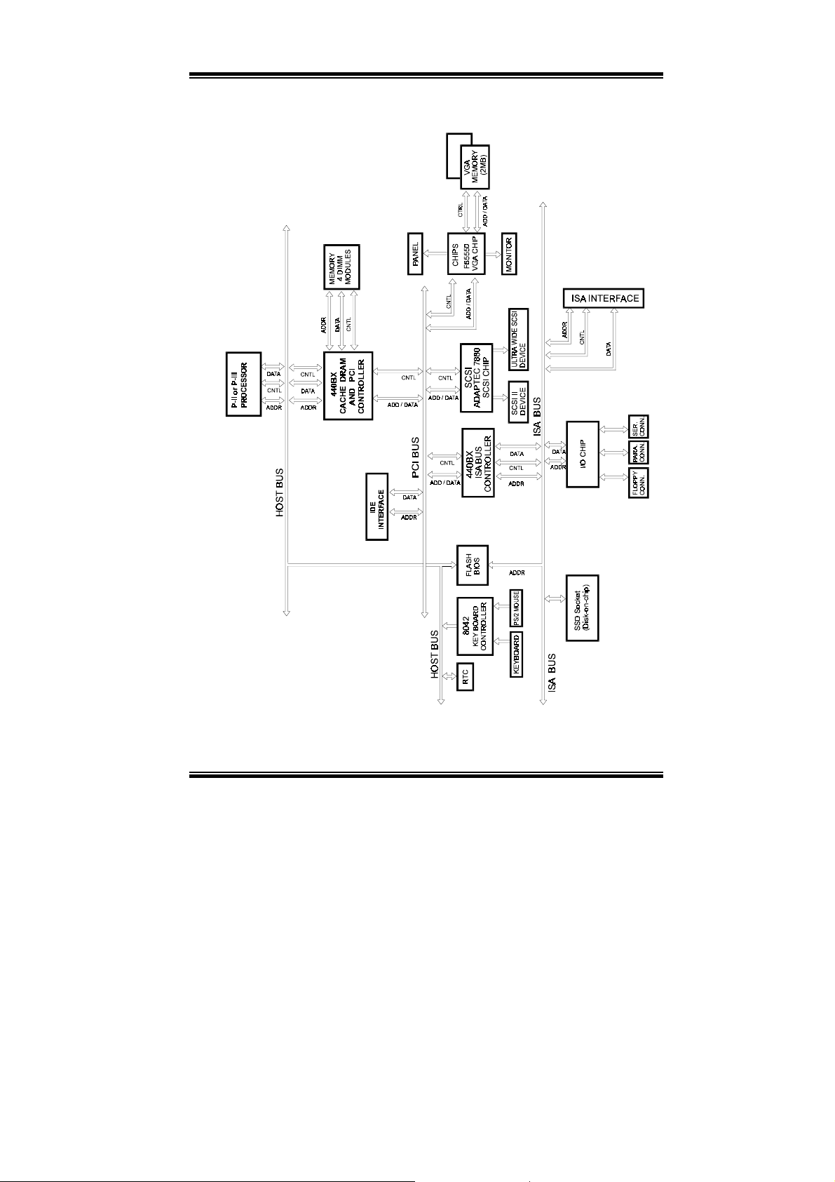
Appendix B Technical Summary
BLOCK DIAGRAM
Page: B-2
′
PC-680 USER
S MANUAL
Page 80

INTERRUPT MAP
IRQ ASSIGNMENT
0 System TIMER interrupt from TIMER-0
1 Keyboard output buffer full
2 Cascade for IRQ 8-15
3 Serial port 2
4 Serial port 1
5 Parallel port 2
6 Floppy Disk adapter
7 Parallel port 1
8 RTC clock
9 Available
10 Available
11 Available
12 Available
13 Math coprocessor
14 Hard Disk adapter
15 Available
Appendix B TECHNICAL SUMMARY
PC-680 USER′S MANUAL
Page: B-3
Page 81

Appendix B Technical Summary
RTC & CMOS RAM MAP
CODE ASSIGNMENT
00 Seconds
01 Second alarm
02 Minutes
03 Minutes alarm
04 Hours
05 Hours alarm
06 Day of week
07 Day of month
08 Month
09 Year
0A Status register A
0B Status register B
0C Status register C
0D Status register D
0E Diagnostic status byte
0F Shutdown byte
10 Floppy Disk drive type byte
11 Reserve
12 Hard Disk type byte
13 Reserve
14 Equipment byte
15 Base memory low byte
16 Base memory high byte
17 Extension memory low byte
18 Extension memory high byte
30 Reserved for extension memory low byte
31 Reserved for extension memory high byte
32 Date Century byte
33 Information Flag
34-3F Reserve
40-7f Reserved for Chipset Setting Data
Page: B-4
′
PC-680 USER
S MANUAL
Page 82

Appendix B TECHNICAL SUMMARY
TIMER & DMA CHANNELS MAP
Timer Channel Map
Timer Channel Assignment
0 System timer interrupt
1 DRAM Refresh request
2 Speaker tone gene rator
DMA Channel Map
DMA Channel Assignment
0 Available
1 IBM SDLC
2 Floppy Disk adapter
3 Channel-3 Available
4 Cascade for DMA controller 1
5 Available
6 Available
7 Available
:
:
PC-680 USER′S MANUAL
Page: B-5
Page 83

Appendix B Technical Summary
I/O & MEMORY MAP
Memory Map :
MEMORY MAP ASSIGNMENT
0000000-009FFFF System memory used by DOS and
application
00A0000-00BFFFF Display buffer memory for VGA/ EGA /
CGA / MONOCHROME adapter
00C0000-00DFFFF Reserved for I/O device BIOS ROM or
RAM buffe r.
00E0000-00EFFFF Reserved for PCI device ROM
00F0000-00FFFFF System BIOS ROM
0100000-FFFFFFF System extension memory
I/O Map :
I/O MAP ASSIGNMENT
000-01F DMA controller (Master)
020-021 Interrupt controller (Master)
022-023 Chipset controller registers I/O ports.
040-05F Timer control regsiters.
060-06F Keyboard interface controller (8042)
070-07F RTC ports & CMOS I/O ports
080-09F DMA register
0A0-0BF Interrupt controller (Slave)
0C0-0DF DMA controller (Slave)
0F0-0FF Math coprocessor
1F0-1F8 Hard Disk controller
278-27F Parallel port-2
2B0-2DF Graphics adapter controller
2F8-2FF Serial port-2
360-36F Net work ports
378-37F Parallel port-1
3B0-3BF Monochrome & Printer adapter
3C0-3CF EGA adapter
3D0-3DF CGA adapter
3F0-3F7 Floppy disk controller
3F8-3FF Serial port-1
Page: B-6
′
PC-680 USER
S MANUAL
Page 84

TROUBLE
SHOOTING
This section outlines the error messages that may occur when you
operate the system. It also gives you the suggestions on solving the
problems.
Sections include:
! Trouble Shooting for Error Messages
! Trouble Shooting for POST Code
APPENDIX
C
Page: C-1
Page 85

Appendix C Trouble Shooting
TROUBLE SHOOTING FOR ERROR MESSAGES
The following information inform you the error messages and the trouble
shooting. Please adjust your systems according to the messages below.
And make sure all the components and connectors are in proper position
and firmly attached. If the errors still encountered, please contact with your
distributor for maintenance.
POST BEEP :
Currently there are two kind of beep codes in BIOS. The one code indicates that a video error has occurred and the BIOS cannot initialize the
video screen to display any additional information. This beep code consists
of a single long beep followed by three short beeps. The other one code
indicates that your DRAM error has occurred. This beep code consists of a
single long beep repeatedly.
CMOS BATTERY FAILURE :
When the CMOS battery is out of work or has run out, the user has to
replace the whole unit.
CMOS CHECKSUM ERROR :
This error inform you that the CMOS is corrupted. When the battery runs
weak, this situation might happen. Please check the battery and change a
new one when necessary.
DISPLAY SWITCH IS SET INCORRECTLY :
Display switch on the motherboard can be set to either monochrome or
color. This indicates the switch is set to a different setting than indicated in
Setup. Determine which setting is correct, and then either turn off the
system and change the jumper, or enter Setup and change the video
selection.
DISK BOOT FAILURE:
When you can‘t find the boot device, insert a system disk into Drive A and
press < Enter >. Make sure both the controller and cables are all in proper
positions, also make sure the disk is formatted correct device. Then reboot
the system.
Page: C-2
PC-680 USER
′
S MANUAL
Page 86

Appendix C Trouble Shooting
DISKETTE DRIVES OR TYPES MISMATCH ERROR :
When the diskette drive type is different from CMOS, please run setup or
configure the drive again.
ERROR ENCOUNTERED INITIALIZING HARD DRIVE :
When you can‘t initialize the hard drive. Assure the adapter is installed
correctly and all cables are correctly and firmly attached. Also be sure the
correct hard drive type is selected in Setup.
ERROR INITIALIZING HARD DISK CONTROLLER :
When this error occurs. Be sure the cord is exactly installed in the bus.
Make sure the correct hard drive type is selected in Setup. Also check
whether all of the jumpers are set correctly in the hard drive.
FLOPPY DISK CONTROLLER ERROR OR
NO CONTROLLER PRESENT :
When you cannot find or initialize the floppy drive controller, please check
the controller whether in proper Setup. If there are no floppy drive
installed, Ensure the Diskette Drive selection in Setup is set to NONE.
KEYBOARD ERROR OR NO KEYBOARD PRESENT
When this situation happens, please check keyboard attachment and no
keys being pressed during the boot. If you are purposely configuring the
system without a keyboard, set the error halt condition in Setup to HALT
ON ALL, BUT KEYBOARD. This will cause the BIOS to ignore the
missing keyboard and continue the boot.
MEMORY ADDRESS ERROR :
When the memory address indicates error. You can use this location along
with the memory map for your system to find and replace the bad memory
chips.
MEMORY SIZE HAS CHANGED :
Memory has been added or removed since the last boot. In EISA mode use
Configuration Utility to reconfigure the memory configuration. In ISA
mode enter Setup and enter the new memory size in the memory fields.
:
PC-680 USER′S MANUAL
Page: C-3
Page 87

Appendix C Trouble Shooting
MEMORY VERIFYING ERROR :
It indicates an error verifying a value already written to memory. Use the
location along with your system's memory map to locate the bad chip.
OFFENDING ADDRESS MISSING :
This message is used in connection with the I/O CHANNEL CHECK and
RAM PARITY ERROR messages when the segment that has caused the
problem cannot be isolated.
REBOOT ERROR :
When this error occurs that requires you to reboot.. Press any key and the
system will reboot.
SYSTEM HALTED :
Indicates the present boot attempt has been aborted and the system must be
rebooted. Press and hold down the CTRL and ALT keys and press DEL.
TROUBLE SHOOTING FOR POST CODES
When you power on your PC, and the screen display nothing. You have to
insert the POST Card for test. The address for ISA POST port is 80h. Make
sure the card is in correct slot. The lists below indicate you the error
messages. Please follow the instruction to adjust your system. If the error
still occurred, please contact with your distributor for maintenance.
Turn off OEM specific cache, shadow.....
C0 :
Initialize all the standard devices with default values Standard devices
03 :
includes :
DMA controller (8237).
Programmable Interrupt Controller (8259).
Programmable Interval Timer (8254).
RTC chip.
1.Keyboard Controller Self-Test.
05 :
2.Enable Keyboard Interface.
Verifies CMOS‘s basic R/W functionality.
07 :
Page: C-4
PC-680 USER
′
S MANUAL
Page 88

Appendix C Trouble Shooting
Program defaults values into chipset according to the MODBINable
BE :
Chipset Default Table.
Auto-detection of onboard DRAM & Cache.
C1 :
Copy the BIOS from ROM into E0000-FFFFF shadow RAM so that POST
C5 :
will go faster.
Test the first 256K DRAM.
08 :
1. Program the configuration register of Cyrix CPU according to the
09 :
MODBINable Cyrix Register Table.
2. OEM specific cache initialization (if needed).
1. Initialize the first 32 interrupt vectors with corresponding Interrupt
0A :
handlers Initialize INT no from 33-120 with Dummy(Spurious) Interrupt
Handler.
2. Issue CPUID instruction to identify CPU type.
3. Early Power Management initialization (OEM specific).
1.Verify the RTC time is valid or not.
0B :
2. Detect bad battery.
3. Read CMOS data into BIOS stack area.
4. PnP initializations including (PnP BIOS only).
-Assign CSN to PnP ISA card.
-Create resource map from ESCD.
5. Assign I/O & Memory for PCI devices (PCI BIOS only).
Initialization of the BIOS Data Area (40 : 0N-40:FF).
0C :
1. Program some of the Chipset‘s value according to Setup. (Early Setup
0D :
Value Program).
2. Measure CPU speed for display & decide the system clock speed.
3. Video initialization including Monochrome ,CGA, EGA/VGA. If no
display device found, the speaker will beep.
PC-680 USER′S MANUAL
Page: C-5
Page 89

Appendix C Trouble Shooting
1. Initialize the APIC (Multi-Processor BIOS only).
0E :
2. Test video RAM (If Monochrome display device found).
3. Show messages including :
-Award Logo, Copyright string, BIOS Date code & Part No.
-OEM specific sign on messages.
-Energy Star Loge (Green BIOS only).
-CPU brand, type & speed.
-Test system BIOS checksum (Non-compress Version only).
DMA channel 0 test.
0F :
DMA channel 1 test.
10 :
DMA page registers test.
11 :
Test 8254 Timer 0 Counter2.
14 :
Test 8259 interrupt mask bits for channel 1.
15 :
Test 8259 interrupt mask bits for channel 2.
16 :
Test 8259 functionality.
19 :
Detect Base Memory & Extended Memory Size.
30 :
1. Test Base Memory from 256K to 640K.
31 :
2. Test Extended Memory from 1M to the top of memory.
1.Display the Award Plug & Play BIOS Extension message (PnP BIOS
32 :
only).
2.Program all onboard super I/O chips (if any) including COM ports, LPT
ports, FDD port....according to setup value.
Set flag to allow users to enter CMOS Setup Utility.
3C :
1 Initialize Keyboard.
3D :
2 Install PS2 mouse.
Page: C-6
PC-680 USER
′
S MANUAL
Page 90

Appendix C Trouble Shooting
Try to turn on Level 2 cache.
3E :
Note : Some chipset may need to turn on the L2 cache in this stage. But
usually, the cache is turn on later in POST 61h.
1. Program the rest of the Chipset‘s value according to Setup. (Later Setup
BF :
Value Program).
2. If auto-configuration is enabled, programmed the chipset with predefined value in the MODBINable Auto-Table.
Initialize floppy disk drive controller.
41 :
Initialize Hard drive controller.
42 :
If it is a PnP BIOS, initialize serial & parallel ports.
43 :
Initialize math coprocessor.
45 :
If there is any error detected (such as video, kb....), show all the error
4E :
messages the screen & wait for user to press <F1> key.
1. If password is needed, ask for password.
4F :
2. Clear the Energy Star Logo (Green BIOS only).
Write all CMOS values currently in the BIOS stack area back into the
50 :
CMOS.
1.Initialize all ISA ROMs.
52 :
2 . Later PCI initializations (PCI BIOS o nly).
-assign IRQ to PCI devices.
-initialize all PCI ROMs.
3 . PnP Initializations (PnP BIOS only).
-assign I/O, Memory, IRQ & DMA TO PnP ISA devices.
-initialize all PnP ISA ROMs.
4. Program shadows RAM according to Setup settings.
5 . Program parity according to Setup setting.
6. Power Management Initialization.
-Enable/Disable global PM.
-APM interface initialization.
PC-680 USER′S MANUAL
Page: C-7
Page 91

Appendix C Trouble Shooting
1.If it is NOT a PnP BIOS, initialize serial & parallel ports.
53 :
2. Initialize time value in BIOS data area by translate the RTC time value
into a timer tick value.
Setup Virus Protection (Boot Sector Protection) functionality according to
60 :
Setup setting.
1. Try to turn on Level 2 cache.
61 :
Note : if L2 cache is already turned on in POST 3D, this part will be
skipped.
2. Set the boot up speed according to Setup setting.
3. Last chance for Chipset initialization.
4. Last chance for Power Management initialization (Green BIOS only).
5. Show the system configuration table.
1.Setup daylight saving according to Setup value.
62 :
2.Program the NumLock, typematic rate & typematic speed according to
Setup setting.
1. If there is any changes in the hardware configuration, update the ESCD
63 :
information (PnP BIOS only).
2. Clear memory that have been used.
3. Boot system via INT 19H.
System Booting. this means that the BIOS already pass the control right to
FF :
the operating system.
Page: C-8
PC-680 USER
′
S MANUAL
Page 92

Appendix C Trouble Shooting
PC-680 USER′S MANUAL
Page: C-9
Page 93

Appendix C Trouble Shooting
Page: C-10
PC-680 USER
′
S MANUAL
Page 94

Appendix C Trouble Shooting
PC-680 USER′S MANUAL
Page: C-11
Page 95

Appendix C Trouble Shooting
Page: C-12
PC-680 USER
′
S MANUAL
Page 96

Appendix C Trouble Shooting
PC-680 USER′S MANUAL
Page: C-13
Page 97

Appendix C Trouble Shooting
PRINTED IN TAIWAN
Page: C-14
PC-680 USER
′
S MANUAL
 Loading...