

Page 1

USER’S
MANUAL
PA-6980 Series
POS System Powered by
Intel® 6th / 7th Gen. Core,
Pentium
®
, Celeron® Processor
PA-6980 Series M5
Page 2

PA-6980 Series POS System
With LCD / Touchscreen
COPYRIGHT NOTICE & TRADEMARK
All trademarks and registered trademarks mentioned herein are the property of their
respective owners.
This manual is copyrighted in May, 2017. You may not reproduce or transmit in any
form or by any means, electronic, or mechanical, including photocopying and
recording.
DISCLAIMER
This user’s manual is meant to assist users in installing and setting up the system. The
information contained in this document is subject to change without any notice.
CE NOTICE
This is a class A product. In a domestic environment this product may cause radio
interference in which case the user may be required to take adequate measures.
Page 3

FCC NOTICE
This equipment has been tested and found to comply with the limits for a Class A
digital device, pursuant to part 15 of the FCC Rules. These limits are designed to
provide reasonable protection against harmful interference when the equipment is
operated in a commercial environment. This equipment generates, uses, and can
radiate radio frequency energy and, if not installed and used in accordance with the
instruction manual, may cause harmful interference to radio communications.
Operation of this equipment in a residential area is likely to cause harmful interference
in which case the user will be required to correct the interference at his own expense.
You are cautioned that any change or modifications to the equipment not expressly
approve by the party responsible for compliance could void your authority to operate
such equipment.
CAUTION! Danger of explosion if battery is incorrectly replaced. Replace only with the same
or equivalent type recommended by the manufacturer. Dispose of used batteries according
to the manufacturer’s instructions.
WARNING! Some internal parts of the system may have high electrical voltage. And
therefore we strongly recommend that qualified engineers can open and disassemble the
system. The LCD and Touchscreen are easily breakable, please handle them with extra
Page 4

Contents
TABLE OF CONTENTS
CHAPTER 1 INTRODUCTION
1-1 About This Manual…........................................................
1-2
1-2 POS System Illustration….................................................
1-3
1-2-1 Panel PC………………………………………...
1-3
1-2-2 Normal Stand……………………………………
1-4
1-2-3 Printer Stand…………………………………….
1-5
1-2-4 Rear I/O View…………………………………...
1-7
1-3 System Specifications…....................................................
1-8
1-4 Safety Precautions….........................................................
1-13
CHAPTER 2 SYSTEM CONFIGURATION
2-1 Jumper & Connector Quick Reference Table…................
2-2
2-2 Main Board Component Locations…...............................
2-4
2-3 How to Set the Jumpers….................................................
2-6
2-4 Main Board Connectors and Jumpers……………………
2-8
2-4-1 COM Port & VGA Connector…………………
2-8
2-4-2 COM Port RI and Voltage Selection…………..
2-11
2-4-3 i-Button Connector…………………………….
2-11
2-4-4 i-Button Function Selection…………………...
2-12
2-4-5 LAN & USB Port………………..……..……...
2-13
2-4-6 Internal USB 2.0 Connector…………………...
2-14
2-4-7 USB 3.0 Connector……………………………
2-15
2-4-8 Cash Drawer Connector………………………..
2-16
2-4-9 Cash Drawer Selection………………………...
2-17
2-4-10 Cash Drawer Power Selection…………………
2-21
2-4-11 2nd Display Power Port………………………..
2-22
2-4-12 Printer Power Port (option)……………….........
2-22
2-4-13 LED Connector………………...........................
2-23
2-4-14 System / CPU Fan Connector……………….....
2-24
2-4-15 Power Input Connector………………………...
2-25
2-4-16 Power Connector………………………............
2-26
2-4-17 Power Switch Connector………………………
2-27
2-4-18 External Speaker Connector…………………...
2-28
2-4-19 Speaker Selection…………………...................
2-29
2-4-20 Inverter Connector…………………..................
2-30
2-4-21 LVDS Connector…………………....................
2-31
Page 5

Contents
2-4-22 LVDS Power Selection…………………...........
2-32
2-4-23 LVDS Backlight Type Selection………………
2-33
2-4-24 MSR / Card Reader Connector………………...
2-34
2-4-25 SATA & SATA Power Connector……………..
2-35
2-4-26 Touch Panel Connector………………………..
2-36
2-4-27 Touch Panel and USB9-1 Selection…………...
2-37
2-4-28 LVDS Output Resolution Selection…………...
2-38
2-4-29 Mini-PCIe / SATA Connector…………………
2-39
2-4-30 Mini-PCIe and USB6 Selection……………….
2-40
2-4-31 Embedded Display Port (EDP) Connector
(option)…………………………………………
2-41
2-4-32 Configuration / Recovery Selection……………
2-42
2-4-33 VCCIO / REFIN Selection…………………….
2-43
2-4-34 Clear CMOS Data Selection…………………..
2-44
2-4-35 GPIO Connector………………….....................
2-45
2-4-36 Audio Jack…………………..............................
2-45
2-5 Printer Board: PDAC-3100……………………………...
2-46
2-5-1 Power Supply Connector………………………
2-48
2-5-2 RS-232 Interface Connector…………………...
2-48
2-5-3 Auto-Cutter Connector…………………...........
2-49
2-5-4 USB Connector…………………......................
2-49
2-5-5 Thermal Head/Motor/Sensor Connector……….
2-50
2-5-6 Terminal Assignment Connector………………
2-52
2-6 Printer Board: MB-1030 series………………………….
2-53
2-6-1 Power Supply Connector………………………
2-55
2-6-2 RS-232 Interface Connector…………………...
2-55
2-6-3 Thermal Head/Motor/Sensor Connector………
2-56
2-6-4 Auto-Cutter Connector………………………...
2-58
2-6-5 Paper-Near-END Sensor Connector…………...
2-58
2-6-6 USB Interface Connector…………....................
2-59
2-6-7 Terminal Assignment Connector…………........
2-59
2-7 Printer Board: MB-1011 & MB-1013…………………...
2-60
2-7-1 Power Supply Connector………………………
2-62
2-7-2 RS-232 Interface Connector…………………...
2-62
2-7-3 Auto-Cutter Connector…………………...........
2-63
2-7-4 Thermal Head/Motor/Sensor Connector……….
2-63
2-7-5 Terminal Assignment Connector………………
2-66
2-7-6 USB Interface Connector………………………
2-66
2-8 VFD Board: MB-4103, LD720………………….............
2-67
2-8-1 Power Switch Selection………………………..
2-69
2-8-2 RS-232 Serial Interface Connector…………….
2-70
Page 6

Contents
2-9 MSR Board: ID TECH…………………..........................
2-71
2-9-1 Main Connector………………………………..
2-71
2-10 MSR Board: MB-3012…………………........................
2-72
2-10-1 Information Button Reader…………………...
2-72
2-10-2 Output Connector………………….................
2-72
CHAPTER 3 SOFTWARE UTILITIES
3-1 Driver…............................................................................
3-2
3-1-1 Introduction……………………………………
3-2
3-1-2 Intel® Chipset Software Installation Utility……
3-3
3-1-3 VGA Driver Utility…………………………….
3-4
3-1-4 LAN Driver Utility…………………………….
3-5
3-1-5 Sound Driver Utility…………………………...
3-6
3-1-6 Touch Screen Driver Utility……………………
3-7
3-1-7 Fingerprint Driver Utility (Optional)………......
3-8
3-2 Peripheral Devices…........................................................
3-9
3-3 API…........................................................ ........................
3-75
3-4 API Functions…................................................................
3-81
CHAPTER 4 AMI BIOS SETUP
4-1 Introduction…...................................................................
4-2
4-2 Entering Setup…...................................................... .........
4-4
4-3 Main……..........................................................................
4-6
4-4 Advanced ……..................................................................
4-8
4-5 Chipset….…………………………….............................
4-33
4-6 Security….........................................................................
4-46
4-7 Boot….……......................................................................
4-47
4-8 Save & Exit…...................................................................
4-51
APPENDIX A SYSTEM ASSEMBLY
Easy Maintenance – HDD…………............................................
A-3
Easy Maintenance – Back Cover………………………………..
A-4
Easy Maintenance – CPU and Memory…………........................
A-6
Exploded Diagrams for 5-wire Analog Resistive Touch Panel:
Exploded Diagram for PA-6980 POS Open & Close…………...
A-7
Exploded Diagram for PA-6980 POS Stand……………………
A-8
Exploded Diagram for PA-6980 120W Power Adapter………
A-9
Exploded Diagram for PA-6980 PPC Open & Close…………...
A-10
Exploded Diagram for PA-6980 Mainboard……………………
A-12
Exploded Diagram for PA-6980 LCD Holder…………………..
A-14
Exploded Diagram for PA-6980 LCD Assembly………………..
A-16
Page 7

Contents
Exploded Diagram for PA-6980 Touch Panel Assembly……….
A-17
Exploded Diagram for PA-6980 HDD Module…………………
A-18
Exploded Diagram for PA-6980 Metal Back Cover…………….
A-19
Exploded Diagram for PA-6980 2.5” SATA HDD……………..
A-20
Exploded Diagrams for Projected Capacitive Touch Panel:
Exploded Diagram for PA-6980 POS Open & Close…………...
A-21
Exploded Diagram for PA-6980 POS Stand……………………
A-22
Exploded Diagram for PA-6980 120W Power Adapter………
A-23
Exploded Diagram for PA-6980 PPC Open & Close…………...
A-24
Exploded Diagram for PA-6980 Mainboard…………………….
A-26
Exploded Diagram for PA-6980 LCD Holder…………………..
A-28
Exploded Diagram for PA-6980 LCD Assembly………………..
A-30
Exploded Diagram for PA-6980 Touch Panel Assembly……….
A-31
Exploded Diagram for PA-6980 HDD Module…………………
A-32
Exploded Diagram for PA-6980 Metal Back Cover…………….
A-33
Exploded Diagram for PA-6980 2.5” SATA HDD……………..
A-34
Exploded Diagram for PA-6980 Printer Module………………..
A-35
Exploded Diagram for PA-6980 MSR Module…………………
A-46
Exploded Diagram for PA-6980 2nd Display…………………...
A-47
Exploded Diagram for PA-6980 VFD Module………………….
A-48
APPENDIX B TECHNICAL SUMMARY
Block Diagram…..........................................................................
B-2
Interrupt Map…............................................................................
B-3
DMA Channels Map….................................................................
B-9
I/O Map…....................................................................................
B-10
Watchdog Timer Configuration…................................................
B-13
Flash BIOS Update………...........................................................
B-16
Page 8

Page:1-1
INTRODUCTION
This chapter gives you the information for the PA-6980. It also outlines
the system specifications.
The following sections are included:
About This Manual
POS System Illustration
- Panel PC
- Normal Stand
- Printer Stand
- Rear I/O View
System Specifications
Safety Precautions
Experienced users can jump to chapter 2 on page 2-1
for a quick start.
CHAPTER
1
Page 9

Chapter 1 Introduction
PA-6980 SERIES USER
S MANUAL
Page: 1-2
1-1. ABOUT THIS MANUAL
Thank you for purchasing our PA-6980 Series System. The PA-6980 is an updated
system designed to be comparable with the highest performance of IBM AT personal
computers. The PA-6980 provides faster processing speed, greater expandability and
can handle more tasks than before. This manual is designed to assist you how to install
and set up the whole system. It contains four chapters and two appendixes. Users can
configure the system according to their own needs.
Chapter 1 Introduction
This chapter introduces you to the background of this manual. It also includes
illustrations and specifications for the whole system. The final section of this chapter
indicates some safety reminders on how to take care of your system.
Chapter 2 System Configuration
This chapter outlines the location of motherboard components and their function. You
will learn how to set the jumper and configure the system to meet your own needs.
Chapter 3 Software Utilities
This chapter contains helpful information for proper installations of the Intel Utility,
VGA Utility, LAN Utility, Sound Utility, Touch Screen Utility and Fingerprint Utility
(Optional).
Chapter 4 AMI BIOS Setup
This chapter indicates you how to change the BIOS configurations.
Appendix A System Assembly
This appendix gives you the exploded diagrams and part numbers of the PA-6980.
Appendix B Technical Summary
This appendix gives you the information about the allocation maps for the system
resources, Watchdog Timer Configuration, and Flash BIOS Update.
Page 10

Chapter 1 Introduction
PA-6980 SERIES USERS MANUAL
Page: 1-3
1-2. POS SYSTEM ILLUSTRATION
Unit: mm
1-2-1. Panel PC
367.49
281.95
74.88
30.43
Page 11

Chapter 1 Introduction
PA-6980 SERIES USER
S MANUAL
Page: 1-4
1-2-2. Normal Stand
1-
Adjustable angle 0-68 degree
87.38
74.88
30.43
280.02
261.65
63.40°
Page 12

Chapter 1 Introduction
PA-6980 SERIES USERS MANUAL
Page: 1-5
1-1-2-3. Printer Stand
367.49
87.38
74.88
30.43
298.42
281.95
60°
398.88
Page 13

Chapter 1 Introduction
PA-6980 SERIES USER
S MANUAL
Page: 1-6
Caution:
Please refer to the picture below to close the printer door properly.
Page 14
Chapter 1 Introduction
PA-6980 SERIES USERS MANUAL
Page: 1-7
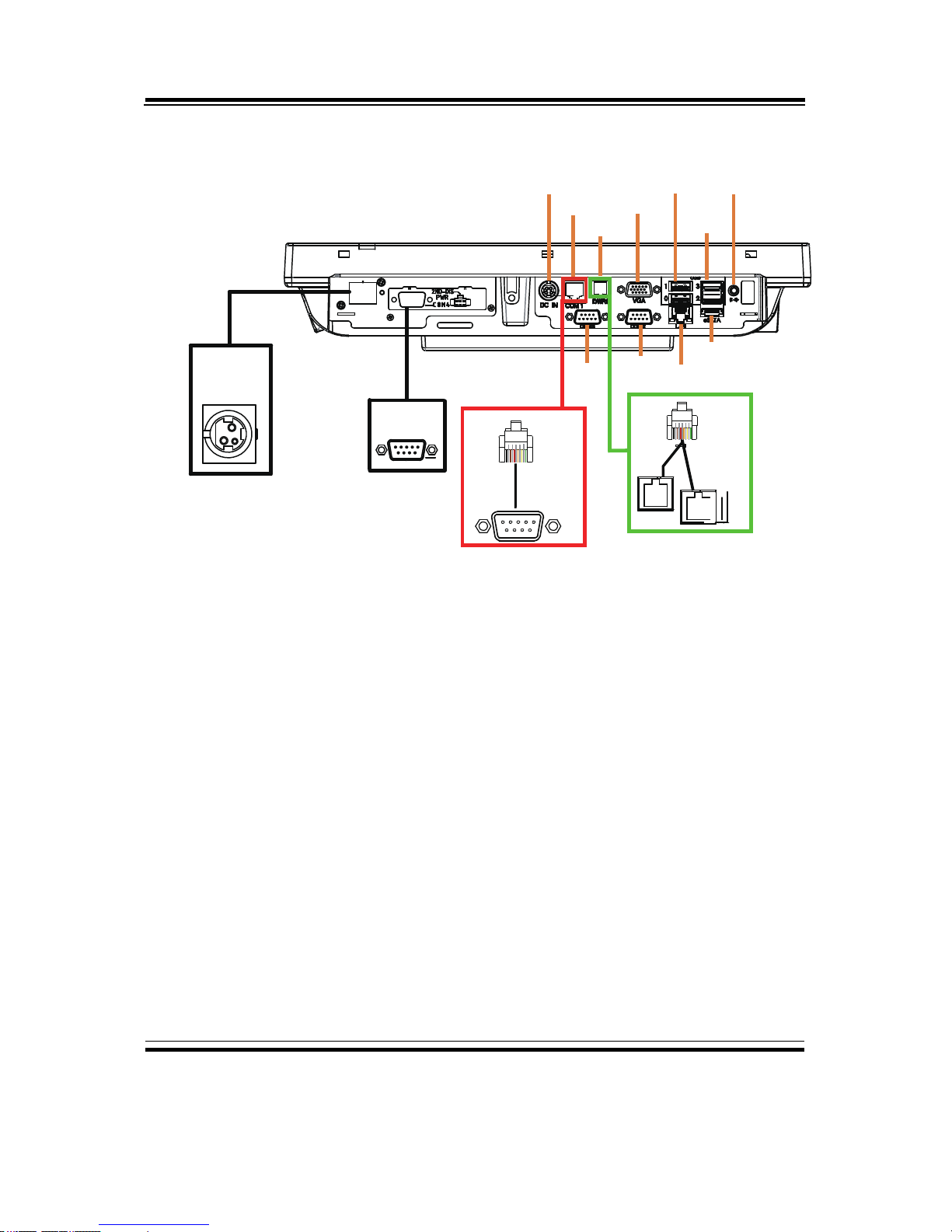
1-2-4. Rear I/O View
PRINT
PWR
COM4
DC IN
RJ11
DRW1-1
DRW
1-2
RJ45
COM
COM1
DRW1
VGA
USB1
USB0
USB2
USB3
LINE-OUT
COM3
COM2
LAN
eSATA
option
option
Page 15

Chapter 1 Introduction
PA-6980 SERIES USER
S MANUAL
Page: 1-8
1-3. SYSTEM SPECIFICATIONS
MAINBOARD (PB-6980)
System
CPU support
6th Gen Skylake 7th Gen Kabylake
• Intel® Core™ i5-6500
• Intel® Core™ i3-6100
• Intel® Pentium® G4400
• Intel® Celeron® G3900
• Intel® Core™ i7-7700
• Intel® Core™ i5-7500
• Intel® Core™ i3-7101E
• Intel® Pentium®
G4560
• Intel® Celeron®
G3930E
Core Logic
Intel® H110 Chipset
Memory
2 x DDR4 SO-DIMM slot (up to 32GB)
Network 10/100/1000Mbps Base-T Fast Ethernet
OS Support • Windows 7 Pro for
Embedded Systems
• Windows Embedded
POSReady 7
• Windows Embedded 8.1
Industry Pro
• Windows 10 IOT
Enterprise
• Windows 10 IOT
Enterprise for Retail or
Thin Client
• Windows 10
• Windows 10 IOT
Enterprise
• Windows 10 IOT
Enterprise for Retail or
Thin Client
BIOS AMI SPI BIOS, 8Mbits with VGA BIOS
Power Supply 120 Watt power inside
System Weight 6.6 kg (POS), 5.3 kg (PPC)
Dimension (W x H x D) • 367.49 x 281.95 x 303.04mm (Normal Stand POS)
• 367.49 x 281.95 x 205.08mm (Printer Stand POS)
• 367.49 x 281.95 x 74.88mm (PPC)
Certificate FCC/CE
Page 16

Chapter 1 Introduction
PA-6980 SERIES USERS MANUAL
Page: 1-9
I/O Ports
USB
• 2 x USB 2.0 ports
• 2 x USB 3.0 ports
eSATA
(external SATA)
• 1 x eSATA port
Serial Port
• 3 x DB-9 (COM 2/3/4(option))
• 1 x RJ-45 (COM1)
• +5V/12V selectable
LAN
1 x RJ-45
VGA
1 x DB-15 VGA Interface
Cash Drawer
1 x RJ-11 (+12V/+24V selectable, default: +12V)
DC IN
1 x 4-pin DC Power Jack
Line-Out
1 x phone jack
Storage
HDD
1 x 2.5” SATA HDD
SSD
1 x 2.5” SATA SSD (Optional)
Display
15” TFT XGA LCD
Max. Resolution: 1024 x 768
Signal Interface: LVDS (18/24bit)
Touchscreen
5-wire Analog resistive or Projected Capacitive
Brightness
• Resistive Touchscreen:
Minimum
160 cd/m2
• Projected Capacitive Touchscreen:
Minimum
180 cd/m2
Tilt Angle
• 0-68 degree with normal stand
• 0-50 degree with printer stand
Page 17

Chapter 1 Introduction
PA-6980 SERIES USER
S MANUAL
Page: 1-10
Environment
Operating Temperature
0˚C ~35˚C (32˚F ~95˚F)
Storage Temperature
-20˚C ~60˚C (-4˚F ~140˚F)
Humidity
20%~90%
Optional Accessories
Printer
2” or 3” easy loading thermal printer with Auto
cutter
MSR & iButton
JIS-I or II, ISO Track1+2+3 (PS/2 interface)
2nd Display
• 8” LCD (Resolution: 800 x 600)
• 10.4” LCD (Resolution: 800 x 600)
• 15” LCD (Resolution: 1024 x 768)
Customer Display
• Interface: RS-232C Baud Rate: 9600/19200 bps
Placement: 20 columns and 2 lines, each column
is 5 x 7 dots
• Standard Code
CP-437, Katakana, CP-737, CP-850, CP-852,
CP-857, CP-860, CP-862, CP-863,CP-865, CP866, CP-1250, CP-1251, CP-1252, CP-1253,
CP-1254, CP-1255, CP-1257
• International Characters
USA, FRANCE, GERMANY, UK, DENMARK
I, SWDEN, ITALY, SPAIN I, JAPAN,
NORWAY, DENMARK II, SPAIN II, LATIN,
KOREA, RUSSIA, SLAVONIC
Page 18

Chapter 1 Introduction
PA-6980 SERIES USERS MANUAL
Page: 1-11
Printer
2” or 3” easy loading thermal printer with autocutter
Printer:
Items
Specifications
Printing method
Thermal dot line printing
Printing accuracy
1mm /5M
Paper feed pitch
0.0625 mm
Maximum Paper-Roll
thickness
80mm
Total dots per line &
Printable dots per
line
2inch 432 dots;
3inch 576 dots
Maximum print
speed
2inch 200 mm/s;
3inch 170 mm/s
Print width
2inch 54 mm;
3inch 72mm
Paper width
2inch 58 +0/-1 mm;
3inch 80 +0/-1 mm
Page 19

Chapter 1 Introduction
PA-6980 SERIES USER
S MANUAL
Page: 1-12
Auto-cutter:
Items
Specifications
Paper cutting method
Slide cutting
Type of paper cutting
Full cut and Partial cut
(1.5 ± 0.5 mm tab left at
the center)
Paper curling
tendency
Fixed blade side and
Movable blade side
Minimum paper core
diameter
φ8 mm (paper thickness:
75μm or thin)
φ18 (paper thickness:
thicker than 75μm)
Minimum paper
cutting length
10 mm
Cutting processing
time
Approx. 0.5 s/cycle
Cutting frequency
1 cut/2 s max.
• Standard Code
CP-437, CP-850, CP-857, CP-737, CP-852, CP860,CP-862, CP-863, CP-865, CP-866, CP1250,CP-1251, CP-1252, CP-1253, CP-1254,
CP-1257, Katakana
• KANJI
JAPANESE (SHIFT-JIS) Code,
TRADITIONAL CHINESE Code
• International Characters
USA, FRANCE, GERMANY, UK, DENMARK
I, SWDEN, ITALY, SPAIN I, JAPAN,
NORWAY, DENMARK II, SPAIN II, LATIN
AMERICA, KOREA, RUSSIA, SLAVONIC
Fingerprint
8-bit grayscale reader
Page 20

Chapter 1 Introduction
PA-6980 SERIES USERS MANUAL
Page: 1-13
1-4. SAFETY PRECAUTIONS
The following messages are safety reminders on how to protect your systems from
damages, and extending the life cycle of the system.
1. Check the Line Voltage
(1) The operating voltage for the power supply should be within the range of
100V to 240V AC; otherwise, the system may be damaged.
2. Environmental Conditions
(1) Place your PA-6980 on a sturdy, level surface. Be sure to allow enough
space around the system to have easy access needs.
(2) Avoid installing your PA-6980 Series POS system in extremely hot or cold
places.
(3) Avoid exposure to sunlight for a long period of time (for example, in a
closed car in summer time. Also avoid the system from any heating device.).
Or do not use the PA-6980 when it has been left outdoors in a cold winter
day.
(4) Bear in mind that the operating ambient temperature is between 0˚C and
35˚C (32˚F and 95˚F).
(5) Avoid moving the system rapidly from a hot place to a cold place, and vice
versa, because condensation may occur inside the system.
(6) Protect your PA-6980 against strong vibrations, which may cause hard disk
failure.
(7) Do not place the system too close to any radio-active device. Radio-active
device may cause signal interference.
(8) Always shut down the operating system before turning off the power.
3. Handling
(1) Avoid placing heavy objects on the top of the system.
(2) Do not turn the system upside down. This may cause the hard drive to
malfunction.
(3) Do no allow any objects to fall into this product.
(4) If water or other liquid spills into the product, unplug the power cord
immediately.
Page 21

Chapter 1 Introduction
PA-6980 SERIES USER
S MANUAL
Page: 1-14
4. Good Care
(1) When the outside case gets stained, remove the stains using neutral washing
agent with a dry cloth.
(2) Never use strong agents such as benzene and thinner to clean the surface of
the case.
(3) If heavy stains are present, moisten a cloth with diluted neutral washing
agent or alcohol and then wipe thoroughly with a dry cloth.
(4) If dust is accumulated on the case surface, remove it by using a special
vacuum cleaner for computers.
Page 22

Page 2-1
SYSTEM
CONFIGURATION
Helpful information that describes the jumper and connector settings,
and component locations.
The following sections are included:
Jumper & Connector Quick Reference Table
Main Board Component Locations
Main Board Configuration and Jumper settings
Main Board Connector Pin Assignments
Printer Board Component Locations & Pin Assignment
Setting Printer Board Connectors and Jumpers
PDAC-3100
MB-3010
MB-1011 & MB-1013
Setting VFD Board Connectors and Jumpers
CHAPTER
2
Page 23

Chapter 2 System Configuration
PA-6980 SERIES USER’S MANUAL
Page: 2-2
2-1. JUMPER & CONNECTOR QUICK REFERENCE TABLE
JUMPER / CONNECTOR
NAME
COM Port and VGA Connector
COM1, COM2, VGA, COM3, COM4 (Option),
COM3_1, COM4_1, COM5
COM Port RI and Voltage
Selection
JP_COM1, JP_COM2, JP_COM3, JP_COM4
i-Button Connector
I-BUT
i-Button Function Selection
JP22, JP23, JP24
LAN & USB Port
LAN, USB0, USB1
Internal USB 2.0 Connector
USB6, USB7, USB8, USB9-1, USB4_1
USB 3.0 Connector
USB2, USB3
eSATA Connector
eSATA
Cash Drawer Connector
DRW1
Cash Drawer Selection
JP17
Cash Drawer Power Selection
JP16
2nd Display Power Port
2nd DIS PWR
Printer Power Port PRINT PWR (option)
LED Connector
PWR_LED, HDD_LED (option)
System / CPU Fan Connector
SYS_FAN1, CPU_FAN1
Power Input Connector
PWR_IN1, PWR_IN2
Power Connector
DC24V, DC12V, DC5V
Power Switch Connector
SW1 (option), SW2
External Speaker Connector
SPK1, SPK2
Speaker Selection
JP13
Inverter Connector
JINV1
LVDS Connector
LVDS1
LVDS Power Selection
JP25
LVDS Backlight Type Selection
JP26
MSR/Card Reader Connector
PS2_1
SATA & SATA Power Connector
SATA1, SATA2, SATA_PWR1, SATA_PWR2
Touch Panel Connector
TOUCH1
Touch Panel and USB9-1
Selection
JP18, JP19
LVDS Output Resolution Selection
JP8, JP9
Mini-PCIe/mSATA Connector
M_PCIE1, M_PCIE2 (option)
Page 24

Chapter 2 System Configuration
PA-6980 SERIES USER’S MANUAL
Page: 2-3
JUMPER / CONNECTOR
NAME
Mini-PCIe and USB6 Selection
JP21
EDP Connector (option)
EDP
Configuration / Recovery Selection
JP11
VCCIO / REFIN Selection
JP10
Clear CMOS Data Selection
JCMOS1
General Purpose Input / Output
(GPIO) Connector
GPIO1
Audio Jack
LINE_OUT1
Page 25

Chapter 2 System Configuration
PA-6980 SERIES USER’S MANUAL
Page: 2-4
2-2. MAIN BOARD COMPONENT LOCATIONS
M/B: PB-6980
PB-6980 Front Connector, Jumper and Component Locations
COM1
COM3
PWR_IN1
PWR_IN2
DRW1
SPK1
JINV1
COM_VGA_
M_PCIE1
ESATA
LAN
D7
3
1
4
1
1
1
5
2
5
1
2
1
1
4
1
2
3
3
5
1
1
5
1
1
3
1
6
6
9
2
1
2
2
4
1
2
5
6
10
6
6
5
10
9
2
5
5
10
5
1
1
3
2
11
20
24
1
2
1
5
6
3
3
6
1
3
29
30
3
2
1
2
1
3
15
5
16
21
1
3
6
5
6
5
1
10
A4
B4
1
2
35
1
8
45
1
1
A5
A4
B4
B5
21
1
1
2
1
10
9
B1
A1
5
5
10
5
6
BE
AU
AA
L
1
A
7
7
12
2
1
2
1
52
6
5
2
6
5
1
3
A9
A1
4
B9
B1
1
2
1
1
1
39
15
17
3
2
40
1
JP23
JP24
JP22
JP16
JP_COM3
JP_COM4
COM3_1
COM4_1
JP_COM1
JP_COM2
COM2
VGA
COM3
DRW1/COM1
LAN
USB0
USB1
eSATA
USB2
PWR_IN1
USB3
LINE-OUT1
DC24V DC5V DC12V
JP11
JCMOS1
JP13
1
4
CPU_FAN1
SW1
EDP
JP21
COM5
SPK1 USB7 PS2_1
I-BUT
USB6
JP26
JINV1
JP25
LVDS
JP8
JP9
SATA1
SATA2
SATA_PWR1
SATA_PWR2
JP10
USB8
USB9-1
JP18
JP19
TOUCH1
SW2
HDD_LED SPK2
GPIO1
M_PCIE1
Intel
H110
REMOVE
Gen. Core™
Intel
®
6th / 7
th
CPU Socket
3
SYS_FAN1
PWR_LED
2
259
145146
143
260
1
SO-DIMM2
(option)
2
1
SO-DIMM1
260
259
144
146
144
145
143
PWR_IN2
BATTERY
1
3
2
JP17
Page 26

Chapter 2 System Configuration
PA-6980 SERIES USER’S MANUAL
Page: 2-5
M_PCIE2 (option)
PB-6980 Rear Connector, Jumper and Component Locations
Page 27

Chapter 2 System Configuration
PA-6980 SERIES USER’S MANUAL
Page: 2-6
2-3. HOW TO SET THE JUMPERS
You can configure your board by setting the jumpers. A jumper consists of two or three
metal pins with a plastic base mounted on the card, and by using a small plastic "cap",
also known as the jumper cap (with a metal contact inside), you are able to connect the
pins. So you can set-up your hardware configuration by "opening" or "closing" pins.
Jumpers can be combined into sets that called jumper blocks. When jumpers are all in
the block, you have to put them together to set up the hardware configuration. The
figure below shows what this looks like.
JUMPERS AND CAPS
If a jumper has three pins for example, labelled PIN1, PIN2, and PIN3. You can
connect PIN1 & PIN2 to create one setting and shorting. You can either connect PIN2
& PIN3 to create another setting. The same jumper diagrams are applied all through
this manual. The figure below shows what the manual diagrams look and what they
represent.
Page 28

Chapter 2 System Configuration
PA-6980 SERIES USER’S MANUAL
Page: 2-7
JUMPER DIAGRAMS
JUMPER SETTINGS
Page 29

Chapter 2 System Configuration
PA-6980 SERIES USER’S MANUAL
Page: 2-8
2-4. MAIN BOARD CONNECTORS AND JUMPERS
2-4-1. COM PORT & VGA CONNECTOR
There are multiple COM ports enhanced in this board namely: COM1, COM2, VGA
Port, COM3, COM3_1, COM4 (option), COM4_1 and COM5.
COM1: COM1 Connector
The pin assignments are as follows:
PIN
ASSIGNMENT
PIN
ASSIGNMENT
1
COM1_DCDJ_I
6
COM1_DSRJ_I
2
COM1_RX_I
7
COM1_RTSJ_I
3
COM1_TX_I
8
COM1_CTSJ_I
4
COM1_DTRJ_I
9
COM1_RI_SEL
5
GND
10
NC
COM2, VGA: COM2 & D-Sub 15-pin VGA Connector
The pin assignments are as follows:
PIN
ASSIGNMENT
PIN
ASSIGNMENT
1
RED
13
HSYNC
2
GREEN
14
VSYNC
3
BLUE
15
DDCA CLK
4
NC
16
DCD2
5
GND
17
RXD2
6
GND
18
TXD2
7
GND
19
DTR2
8
GND
20
GND
9
+5V
21
DSR2
10
GND
22
RTS2
11
NC
23
CTS2
12
DDCA DATA
24
RI/+5V/+12
selectable
COM1
COM2/
VGA
Page 30

Chapter 2 System Configuration
PA-6980 SERIES USER’S MANUAL
Page: 2-9
COM3/COM4 (Option): COM3, COM4 Connector
The pin assignments are as follows:
PIN
ASSIGNMENT
PIN
ASSIGNMENT
1
COM3_DCDJ_I
6
COM3_DSRJ_I
2
COM3_RX_I
7
COM3_RTSJ_I
3
COM3_TX_I
8
COM3_CTSJ_I
4
COM3_DTRJ_I
9
RI / +5V / +12V
selectable
5
GND
-
-
COM3 and COM3_1 can't be used simultaneously.
COM4 and COM4_1 can't be used simultaneously.
COM3_1: COM3_1 Connector
The pin assignments are as follows:
PIN
ASSIGNMENT
PIN
ASSIGNMENT
1
COM3_DCDJ_I
6
COM3_DSRJ_I
2
COM3_RX_I
7
COM3_RTSJ_I
3
COM3_TX_I
8
COM3_CTSJ_I
4
COM3_DTRJ_I
9
COM3_RI_SEL
5
GND
10
NC
COM4_1: COM4_1 Connector
The pin assignments are as follows:
PIN
ASSIGNMENT
PIN
ASSIGNMENT
1
COM4_DCDJ_I
6
COM4_DSRJ_I
2
COM4_RX_I
7
COM4_RTSJ_I
3
COM4_TX_I
8
COM4_CTSJ_I
4
COM4_DTRJ_I
9
COM4_RI_SEL
5
GND
10
NC
COM3/
COM4
(Option)
1
10
5
6
COM3_1
1
10
5
6
COM4_1
Page 31

Chapter 2 System Configuration
PA-6980 SERIES USER’S MANUAL
Page: 2-10
COM5: COM5 Connector
The pin assignments are as follows:
PIN
ASSIGNMENT
PIN
ASSIGNMENT
1
COM5_DCDJ_I
6
COM5_DSRJ_I
2
COM5_RX_I
7
COM5_RTSJ_I
3
COM5_TX_I
8
COM5_CTSJ_I
4
COM5_DTRJ_I
9
COM5_RI_SEL
5
GND
10
NC
1
10
5
6
COM5
Page 32

Chapter 2 System Configuration
PA-6980 SERIES USER’S MANUAL
Page: 2-11
2-4-2. COM PORT RI & VOLTAGE SELECTION
JP_COM1 , JP_COM2, JP_COM3, JP_COM4: COM Port RI & Voltage Selection,
pin-headers on board. The voltage of COM1, COM2, COM3 and COM4 is made to
control by the jumpers on board.
The jumper settings are as follows:
SELECTION
JUMPER SETTING
JUMPER ILLUSTRATION
RI
1-2
VCC12
3-4
VCC
5-6
Note: Manufacturing Default is RI.
2-4-3. i-BUTTON CONNECTOR
I-BUT: i-Button Connector
The pin assignments are as follows:
PIN
ASSIGNMENT
1
COM3_DTR_R_I
2
COM3_RXD_R_I
I-BUT
Page 33

Chapter 2 System Configuration
PA-6980 SERIES USER’S MANUAL
Page: 2-12
2-4-4. i-BUTTON FUNCTION SELECTION
JP22, JP23, JP24: i-Button Function Selection
The jumper settings are as follows:
SELECTION
JUMPER SETTING
JUMPER ILLUSTRATION
COM2
1-2
1
JP22/JP23/JP24
i-Button*
2-3
1
JP22/JP23/JP24
Note: Manufacturing Default is COM2.
*When these jumpers are set as ‘i-Button’, the COM3_1 connector will not function.
Page 34

Chapter 2 System Configuration
PA-6980 SERIES USER’S MANUAL
Page: 2-13
2-4-5. LAN & USB PORT
LAN & USB0, USB1 Connector
The pin assignments are as follows:
USB0 and USB1: USB 2.0 Connector, USB Type A ports
PIN
ASSIGNMENT
PIN
ASSIGNMENT
A1
VCC5
B1
VCC5
A2
USB0-
B2
USB1-
A3
USB0+
B3
USB1+
A4
GND
B4
GND
LAN: a Giga LAN RJ-45 port (rear I/O)
PIN
ASSIGNMENT
PIN
ASSIGNMENT
1
LAN1_MDI0_DP
5
LAN1_MDI2_DP
2
LAN1_MDI0_DN
6
LAN1_MDI2_DN
3
LAN1_MDI1_DP
7
LAN1_MDI3_DP
4
LAN1_MDI1_DN
8
LAN1_MDI3_DN
Left Side LAN LED Indicator
Orange Color Blinking
LAN Message Active
Off
No LAN Message Active
Right Side LAN LED Indicator
Green Color On
10/100Mbps LAN Speed Indicator
Orange Color On
Giga LAN Speed Indicator
Off
No LAN switch / hub connected
LAN/
USB0/
USB1
Page 35

Chapter 2 System Configuration
PA-6980 SERIES USER’S MANUAL
Page: 2-14
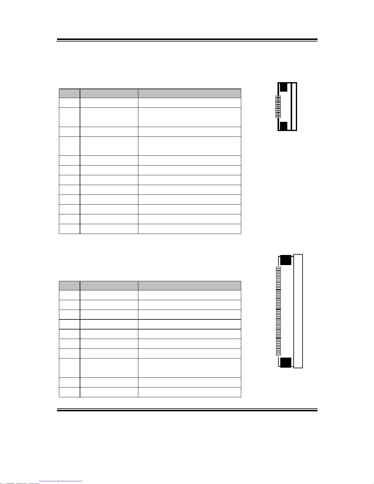
2-4-6. Internal USB 2.0 CONNECTOR
USB6, USB7, USB9-1: Internal USB 2.0 connector
The pin assignments are as follows:
PIN
ASSIGNMENT
1
5V (Maximum current: 0.5A)
2
D- 3 D+ 4 GND
5
GND
Note:
USB6 signal is shared from "MINI-PCIE" port.
USB6 could be functioned when JP21 are set 1-3, 2-4 [short].
USB9-1 signal is shared from "MINI-PCIE" port.
USB9-1 could be functioned when JP18, JP19 are set 1-2 [short].
USB6/
USB7
USB9-1
Page 36

Chapter 2 System Configuration
PA-6980 SERIES USER’S MANUAL
Page: 2-15
2-4-7. USB 3.0 CONNECTOR
USB2: USB 3.0 connector
The pin assignments are as follows:
PIN
ASSIGNMENT
PIN
ASSIGNMENT
1
VCC5
6
RX2_DP
2
USBP3N
7
GND
3
USBP3P
8
TX3_DN
4
GND
9
TX3_DP
5
RX2_DN
10
-
USB3: USB 3.0 connector
The pin assignments are as follows:
PIN
ASSIGNMENT
PIN
ASSIGNMENT
1
VCC5
6
BP_RX_DP
2
USBP4N
7
GND
3
USBP4P
8
BP_TX_DN
4
GND
9
BP_TX_DP
5
BP_RX_DN
10
-
eSATA (external SATA): a combo eSATA/USB 3.0 connector
The pin assignments are as follows:
PIN
ASSIGNMENT
PIN
ASSIGNMENT
1
GND
5
SATA_RXN_2_C
2
SATA_TXP_2_C
6
SATA_RXP_2_C
3
SATA_TXN_2_C
7
GND
4
GND
-
-
eSATA (external Serial Advanced Technology Attachment) is a 7-wire/7-pin
technology. The maximum cable length is 6 1/2 feet (2 meters). eSATA and SATA
have the same number of wires/pins and their signal formats are the same
USB2/
USB3
Page 37

Chapter 2 System Configuration
PA-6980 SERIES USER’S MANUAL
Page: 2-16
2-4-8.CASH DRAWER CONNECTOR
DRW1: RJ-11 Cash Drawer Connector (+12V/+24V selectable, default: +12V).
DRW1 is used by default.
The pin assignments are as follows:
PIN
ASSIGNMENT
1
DRW2 Sense
2
GPIO1 / DRW1
3
DRW1 Sense
4
12V/24V (Max. current 1A)
5
GPIO2 / DRW2
6
GND
1 6
DRW1
Page 38

Chapter 2 System Configuration
PA-6980 SERIES USER’S MANUAL
Page: 2-17
2-4-9. CASH DRAWER SELECTION
JP17: DRW1, DRW1-1, DRW1-2
DRW1 port is used by default. You can add a
second port via either of the methods below:
Method 1:
DRW1 includes two groups of GPIO pins.
The second group is normally unused but can be
enabled by the jumper. Set the pin header jumper
JP17 as 1-2 connected if necessary.
Method 2:
You can split DRW1 into two channels of DRW1-1 & DRW1-2 using the Y-Cable
(option).
JP17: Cash Drawer 2 Selection
SELECTION
JUMPER SETTING
JUMPER ILLUSTRATION
Casher
Drawer 2
1-2
JP17
Casher
Drawer1
2-3
JP17
Note: Manufacturing Default is Cash Drawer 1.
Page 39

Chapter 2 System Configuration
PA-6980 SERIES USER’S MANUAL
Page: 2-18
Step 3.
DRW1, DRW1-1, DRW1-2 shares the same power source.
(Default: 12V).
SIO Address
Cash drawer 1
LDN 06, 0xA1 bit 4
Cash drawer 2
LDN 06, 0xA1 bit 5
Cash Drawer Configuration
The I/O port address of the cash drawer is 2E (hex) and 2F (hex). 2E (hex) is
the address port. 2F (hex) is the data port. User must first assign the address of
register by writing address value into address port 2E (hex), then write/read
data to/from the assigned register through data port 2F (hex).
Configuration Sequence
To program F81866 configuration registers, the following configuration
sequence must be followed:
(1) Enter the extended function mode
(2) Configure the configuration registers
(3) Exit the extended function mode
(1) Enter the extended function mode
To place the chip into the Extended Function Mode, two successive writes of
0x87 must be applied to Extended Function Enable Registers (EFERs, i.e. 2Eh
or 4Eh).
RJ11
DRW1-1
DRW
1-2
Page 40

Chapter 2 System Configuration
PA-6980 SERIES USER’S MANUAL
Page: 2-19
(2) Configure the configuration registers
The chip selects the Logical Device and activates the desired Logical Devices
through Extended Function Index Register (EFIR) and Extended Function Data
Register (EFDR). The EFIR is located at the same address as the EFER, and
the EFDR is located at address (EFIR+1). First, write the Logical Device
Number (i.e. 0x06) to the EFIR and then write the number of the desired Logical
Device to the EFDR. If accessing the Chip (Global) Control Registers, this step
is not required. Secondly, write the address of the desired configuration register
within the Logical Device to the EFIR and then write (or read) the desired
configuration register through the EFDR.
(3) Exit the extended function mode
To exit the Extended Function Mode, writing 0xAA to the EFER is required.
Once the chip exits the Extended Function Mode, it is in the normal running
mode and is ready to enter the configuration mode.
Code example for open the cash drawer 1
;------ Enter to extended function mode -----------------------------------------------------
mov dx, 2eh
mov al, 87h
out dx, al
out dx, al
;------ Select Logical Device 6 of Cash drawer --------------------------------------------
mov al, 07h
out dx, al
inc dx
mov al, 06h
out dx, al
dec dx
;------ Open Cash drawer 1 --------------------------------------------
mov al, A1h
out dx, al
inc dx
in al, dx
or al, 10h
out dx, al
;------ Close Cash drawer 1 --------------------------------------------
in al, dx
and al, EFh
out dx, al
Page 41

Chapter 2 System Configuration
PA-6980 SERIES USER’S MANUAL
Page: 2-20
;------ Exit the extended function mode -----------------------------------------------------
dec dx
mov al, 0aah
out dx, al
Note:
The DRW2 Port can function only when the optional "Printer Kit" is installed on PA-
6980. The DRW2 signals from the printer board (MB-1030, MB-1011, MB-1013,
PDAC-3100) can be controlled via relevant commands. The DRW2 port is located at
the bottom of the Printer Stand connected with a cable (optional) as shown below:
Printer Stand Bottom View
PIN
ASSIGNMENT
PIN
ASSIGNMENT
1
GND
4
+24V
2
Drawer Open
5
NC 3 Drawer Sense
6
GND
Control Codes
Hexadecimal
Codes
Function
<DLE EOT>
10 04
Real-time status
transmission
<DLE DC4>
10 14
Real-time output of the
specified pulse
DRW2
Page 42

Chapter 2 System Configuration
PA-6980 SERIES USER’S MANUAL
Page: 2-21
2-4-10. CASH DRAWER POWER SELECTION
JP16: Cash Drawer Power Selection
The jumper settings are as follows:
SELECTION
JUMPER SETTING
JUMPER ILLUSTRATION
24V
1-2
1
JP16
12V
2-3
1
JP16
Note: Manufacturing Default is 12V.
Page 43

Chapter 2 System Configuration
PA-6980 SERIES USER’S MANUAL
Page: 2-22
2-4-11. 2nd Display Power Port
2nd DIS PWR: DC12V power supply for 2nd display.
PIN
ASSIGNMENT
PIN
ASSIGNMENT
1
VCC12
3
NC
2
GND
-
-
2-4-12. Printer Power Port (Option)
PRINT PWR: DC24V power supply for the stand-printer.
PIN
ASSIGNMENT
P1 P2
+24V
P3
2nd DIS
PWR
PRINTER
POWER
(Option)
GND
+24V
Page 44

Chapter 2 System Configuration
PA-6980 SERIES USER’S MANUAL
Page: 2-23
2-4-13. LED CONNECTOR
PWR_LED: Power indication LED Connector
The pin assignments are as follows:
PIN
ASSIGNMENT
1
VCC5
2
GND
HDD_LED (option): HDD indication LED Connector
The pin assignments are as follows:
PIN
ASSIGNMENT
1
VCC3_3
2
PCH_SATA_LED_N
PWR_LED
HDD_LED
(option)
Page 45

Chapter 2 System Configuration
PA-6980 SERIES USER’S MANUAL
Page: 2-24
2-4-14. SYSTEM / CPU FAN CONNECTOR
SYS_FAN1: System Fan Connector 1
The pin assignments are as follows:
PIN
ASSIGNMENT
1
GND
2
VCC12
3
SYS_FANIN
4
SYS_FANOUT
CPU_FAN1: CPU Fan Connector 1
PIN
ASSIGNMENT
1
GND
2
VCC12
3
CPU_FANIN
4
CPU_FANOUT
4
1
SYS_FAN1
CPU_FAN1
Page 46

Chapter 2 System Configuration
PA-6980 SERIES USER’S MANUAL
Page: 2-25
2-4-15. POWER INPUT CONNECTOR
PWR_IN1: Power Input Connector 1
The pin assignments are as follows:
PIN
ASSIGNMENT
1
GND
2
GND
3
24VIN
4
24VIN
PWR_IN2: Power Input Connector 2
The pin assignments are as follows:
PIN
ASSIGNMENT
1
GND
2
24VIN
3
24VIN
4
GND
PWR_IN1
PWR_IN2
Page 47

Chapter 2 System Configuration
PA-6980 SERIES USER’S MANUAL
Page: 2-26
2-4-16. POWER CONNECTOR
DC24V: Power for Thermal Printer Connector
The pin assignments are as follows:
DC12V: DC 12Voltage Provider Connector
The pin assignments are as follows:
PIN
ASSIGNMENT
1
VCC12_GT
2
NC 3 GND
DC5V: DC 5Voltage Provider Connector
The pin assignments are as follows:
PIN
ASSIGNMENT
1
V_5P0_A
2
GND
PIN
ASSIGNMENT
1
24VIN
2
24VIN
3
GND
4
GND
DC24V
DC5V
1 3
DC12V
Page 48

Chapter 2 System Configuration
PA-6980 SERIES USER’S MANUAL
Page: 2-27
2-4-17. POWER SWITCH CONNECTOR
SW1: Power Switch Connector 1
The pin assignments are as follows:
PIN
ASSIGNMENT
1
GND
2
LPC_PWRBTNJ
3
GND
4
GND
SW2: Power Switch Connector 2
The pin assignments are as follows:
PIN
ASSIGNMENT
1
LPC_PWRBTNJ
2
GND
SW2
SW1
(option)
Page 49

Chapter 2 System Configuration
PA-6980 SERIES USER’S MANUAL
Page: 2-28
2-4-18. EXTERNAL SPEAKER CONNECTOR
SPK1: External Speaker Connector
The pin assignments are as follows:
PIN
ASSIGNMENT
1
HD_FRONT-OUT1-R
2
HD_FRONT-OUT1-L
SPK2 (option): External Speaker Connector
The pin assignments are as follows:
PIN
ASSIGNMENT
1
HD_FRONT-OUT2-R
2
HD_FRONT-OUT2-L
1
2
SPK1/
SPK2
(option)
Page 50

Chapter 2 System Configuration
PA-6980 SERIES USER’S MANUAL
Page: 2-29
2-4-19. SPEAKER SELECTION
JP13: SPK1/SPK2 Selection
The jumper settings are as follows:
SELECTION
JUMPER SETTING
JUMPER ILLUSTRATION
SPK1&SPK2
1-2
1
JP13
Only SPK1
Open
JP13
Note: Manufacturing Default is SPK1&SPK2.
Page 51

Chapter 2 System Configuration
PA-6980 SERIES USER’S MANUAL
Page: 2-30
2-4-20. INVERTER CONNECTOR
JINV1: Inverter Connector
The pin assignments are as follows:
PIN
ASSIGNMENT
1
GND
2
VCC12
3
VCC12
4
VCC12
5
GND
6
LED_PWM
7
GND
8
PANLE_BKLTEN
1
8
JINV1
Page 52

Chapter 2 System Configuration
PA-6980 SERIES USER’S MANUAL
Page: 2-31
2-4-21. LVDS CONNECTOR
LVDS1: LVDS Connector
The pin assignments are as follows:
PIN
ASSIGNMENT
PIN
ASSIGNMENT
1
LVDS_VCC
16
LVDS_CLKAP
2
GND
17
LVDS_CLKAM
3
LVDS_CLKBM
18
GND
4
LVDS_CLKBP
19
LVDS_YAP2
5
GND
20
LVDS_YAM2
6
LVDS_YBM2
21
GND
7
LVDS_YBP2
22
LVDS_YAP1
8
GND
23
GND
9
LVDS_YBM1
24
GND
10
LVDS_YBP1
25
LVDS_YAP0
11
LVDS_YBP3
26
LVDS_YAM0
12
LVDS_YBM3
27
LVDS_YAP3
13
LVDS_YBP0
28
LVDS_YAM3
14
LVDS_YBM0
29
LVDS_VCC
15
GND
30
LVDS_VCC
Page 53

Chapter 2 System Configuration
PA-6980 SERIES USER’S MANUAL
Page: 2-32
2-4-22. LVDS POWER SELECTION
JP25: LVDS Power Selection
The jumper settings are as follows:
SELECTION
JUMPER SETTING
JUMPER ILLUSTRATION
3.3V
1-2
1
JP25
5V
2-3
1
JP25
Note: Manufacturing Default is 3.3V.
Page 54

Chapter 2 System Configuration
PA-6980 SERIES USER’S MANUAL
Page: 2-33
2-4-23. LVDS BACKLIGHT TYPE SELECTION
JP26: LVDS Backlight Type Selection
The jumper settings are as follows:
SELECTION
JUMPER SETTING
JUMPER ILLUSTRATION
3.3V
1-2
JP26
5V
2-3
JP26
Note: Manufacturing Default is 3.3V.
Page 55

Chapter 2 System Configuration
PA-6980 SERIES USER’S MANUAL
Page: 2-34
2-4-24. MSR/CARD READER CONNECTOR
PS2_1: MSR/Card Reader Connector
The pin assignments are as follows:
PIN
ASSIGNMENT
1
KCLK_KB (Output)
2
KCLK_C (Input)
3
KDAT_C (Input)
4
KDAT_KB (Output)
5
+5V
6
GND
PS2_1
Page 56

Chapter 2 System Configuration
PA-6980 SERIES USER’S MANUAL
Page: 2-35
2-4-25. SATA & SATA POWER CONNECTOR
SATA1, SATA2 (option): Serial ATA Connectors
The pin assignments are as follows:
PIN
ASSIGNMENT
1
G1 2 TX+
3
TX-
4
G2 5 RX-
6
RX+
7
G3
SATA_PWR1, SATA_PWR 2 (option): Serial ATA Power Connectors
The pin assignments are as follows:
PIN
ASSIGNMENT
1
VCC
2
GND
3
GND
4
VCC12
SATA1/
SATA2
(option)
SATA_PWR1
SATA_PWR2
(option)
Page 57

Chapter 2 System Configuration
PA-6980 SERIES USER’S MANUAL
Page: 2-36
2-4-26. TOUCH PANEL CONNECTOR
TOUCH1: Touch Panel Connector
The pin assignments are as follows:
PIN
ASSIGNMENT
1
L+ 2 L-
3
COM
4
U+
5
U-
TOUCH1
Page 58

Chapter 2 System Configuration
PA-6980 SERIES USER’S MANUAL
Page: 2-37
2-4-27. TOUCH PANEL & USB9-1 SELECTION
JP18, JP19: Touch Panel and USB9-1 Selection
The jumper settings are as follows:
SELECTION
JUMPER SETTING
JUMPER ILLUSTRATION
USB9-1
Connector
(Capacitor Panel
Selection)
1-2
1
JP18/JP19
USB Interface
(Resistor Panel
Selection)
2-3
1
JP18/JP19
Note: Manufacturing Default is USB interface.
Page 59

Chapter 2 System Configuration
PA-6980 SERIES USER’S MANUAL
Page: 2-38
2-4-28. LVDS OUTPUT RESOLUTION SELECTION
JP8 & JP9: LVDS Output Resolution Selection
SELECTION
JUMPTER
SETTING
JUMPER ILLUSTRATION
1024x768
(24 bit)
JP8(3-5)
JP8(2-4)
JP9(3-5)
JP9 (4-6)
JP8
JP9
1024x768
(18 bit)
JP8(1-3)
JP8(4-6)
JP9(3-5)
JP9(4-6)
JP8
JP9
800x600
(18 bit)
JP8(3-5)
JP8(4-6)
JP9(3-5)
JP9(4-6)
JP8
JP9
Page 60

Chapter 2 System Configuration
PA-6980 SERIES USER’S MANUAL
Page: 2-39
2-4-29. Mini-PCIe/mSATA CONNECTOR
M_PCIE1, M_PCIE2(option):
MINI PCIE/mSATA Connector.
The pin assignments are as follows:
PIN
ASSIGNMENT
PIN
ASSIGNMENT
1
WAKE#
27
GND
2
+3.3V
28
+1.5V
3
Reserved
29
GND
4
GND
30
SMB_CLK
5
Reserved
31
PETn2
6
+1.5V
32
SMB_DATA
7
CLKREQ#
33
PETp2
8
Reserved
34
GND
9
GND
35
GND
10
Reserved
36
USB D-
11
REFCLK1-
37
GND
12
Reserved
38
USB D+
13
REFCLK1+
39
+3.3V
14
Reserved
40
GND
15
GND
41
+3.3V
16
Reserved
42
Reserved
17
Reserved
43
GND
18
GND
44
Reserved
19
Reserved
45
NC
20
Reserved
46
Reserved
21
GND
47
NC
22
PERST#
48
+1.5V
23
PERn0
49
NC
24
+3.3SB
50
GND
25
PERp0
51
Reserved
26
GNd
52
+3.3V
M_PCIE1/
M_PCIE2(option)
Page 61

Chapter 2 System Configuration
PA-6980 SERIES USER’S MANUAL
Page: 2-40
2-4-30. Mini-PCIe and USB6 Selection
JP21: Mini-PCIe and USB6 Selection
The selection is as follows:
SELECTION
JUMPER SETTING
JUMPER ILLUSTRATION
USB signal to
USB6 wafer
1-3, 2-4
JP21
USB6
(Disabled)
signal to
mini-PCIe
3-5, 4-6
JP21
Note: Manufacturing Default is USB6 (Disabled) signal to mini-PCIe.
Page 62

Chapter 2 System Configuration
PA-6980 SERIES USER’S MANUAL
Page: 2-41
2-4-31. Embedded Display Port (EDP) CONNECTOR (option)
EDP: EDP Connector
The pin assignments are as follows:
PIN
ASSIGNMENT
PIN
ASSIGNMENT
1
NC
21
VCC3_3
2
GND
22
NC 3 EDP_TX3_DN
23
GND
4
EDP_TX3_DP
24
GND
5
GND
25
GND
6
EDP_TX2_DN
26
GND
7
EDP_TX2_DP
27
EDP_LVDS_HPD
8
GND
28
GND
9
EDP_TX1_DN
29
GND
10
EDP_TX1_DP
30
GND
11
GND
31
GND
12
EDP_TX0_DN
32
EDP_BKLTEN
13
EDP_TX0_DP
33
EDP_BKLTCTL
14
GND
34
NC
15
EDP_AUX_DP_C
35
NC
16
EDP_AUX_DN_C
36
VCC12
17
GND
37
VCC12
18
VCC3_3
38
VCC12
19
VCC3_3
39
VCC12
20
VCC3_3
40
NC
eDP (Embedded DisplayPort) was developed to be used specifically in embedded
display applications, such as Notebook and Notepad PCs. eDP is based on the VESA
DisplayPort Standard. It aims to define a standardized display panel interface for
internal connections; e.g., graphics cards to notebook display panels. It has advanced
power-saving features including seamless refresh rate switching. It has become the new
mainstream display panel interface for LCD panels with the realized higher resolution.
EDP
Page 63

Chapter 2 System Configuration
PA-6980 SERIES USER’S MANUAL
Page: 2-42
2-4-32. CONFIGURATION / RECOVERY SELECTION
JP11: Configuration / Recovery Selection
The jumper settings are as follows:
SELECTION
JUMPER SETTING
JUMPER ILLUSTRATION
Normal
1-2
JP11
Configure
2-3
JP11
Recovery
Open
JP11
Page 64

Chapter 2 System Configuration
PA-6980 SERIES USER’S MANUAL
Page: 2-43
2-4-33. VCCIO / REFIN SELECTION
JP10: VCCIO / Refine Selection
The jumper settings are as follows:
SELECTION
JUMPER SETTING
JUMPER ILLUSTRATION
1.0V
1-2
JP10
0.95V
2-3
JP10
1.0V
Open
JP10
Note: Manufacturing Default is 1.0V.
Page 65

Chapter 2 System Configuration
PA-6980 SERIES USER’S MANUAL
Page: 2-44
2-4-34. CLEAR CMOS DATA SELECTION
JCMOS1: Clear CMOS Data Selection
SELECTION
JUMPTER
SETTING
JUMPER ILLUSTRATION
Normal
Open
JCMOS1
Clear CMOS
Data
1-2
JCMOS1
Note 1: Manufacturing Default is Normal.
Note 2: To clear CMOS data, users must power off the computer and set the jumper to
“Clear CMOS Data” as shown above. After five to six seconds, set the jumper
back to “NC” and power on the computer.
Page 66

Chapter 2 System Configuration
PA-6980 SERIES USER’S MANUAL
Page: 2-45
2-4-35. GPIO CONNECTOR
GPIO1: General Purpose Input / Output Connector
The pin assignments are as follows:
PIN
ASSIGNMENT
1
3.3V(Maximum current: 0.5A)
2
GND
3
GPIO
2-4-36. AUDIO JACK
LINE_OUT1: External audio phone jack port
The pin assignments are as follows:
PIN
ASSIGNMENT
1
HD_GND
2
LINE-OUT-R
3
NC 4 VCC_AUD
5
LINE-OUT-L
1
3
GPIO1
LINE_OUT1
Page 67

Chapter 2 System Configuration
PA-6980 SERIES USER’S MANUAL
Page: 2-46
Printer Board Component Locations & Pin Assignment
2-5. Printer Board: PDAC-3100 (Option)
CN5
CN8
CN7
CN6
CN3
CN1
14
1
1
13
7
1
12
CN2
1
50
1
5
1
4
Figure 2-1. PDAC-3100 Printer Board Component Locations
Page 68

Chapter 2 System Configuration
PA-6980 SERIES USER’S MANUAL
Page: 2-47
Jumper & Connector Quick Reference Table
Jumper / Connector
NAME
Power Supply Connector
CN1
RS-232 Interface Connector
CN7
Auto-Cutter Connector
CN3
USB Connector
CN8
Thermal Head/Motor/Sensor Connector
CN2
Terminal Assignment Connector
CN5
Page 69

Chapter 2 System Configuration
PA-6980 SERIES USER’S MANUAL
Page: 2-48
Setting Printer Board Connectors and Jumpers: PDAC-3100
2-5-1. Power Supply Connector
CN1: Power supply wafer
PIN
ASSIGNMENT
1
+24V
2
+24V
3
GND
4
GND
2-5-2. RS-232 Interface Connector
CN7: RS-232 interface connector
PIN
ASSIGNMENT
PIN
ASSIGNMENT
1
TXD
5
DTR
2
RXD
6
DSR
3
RTS
7
GND
4
CTS
-
-
4
1
CN1
1
7
CN7
Page 70

Chapter 2 System Configuration
PA-6980 SERIES USER’S MANUAL
Page: 2-49
2-5-3. Auto-Cutter Connector
CN3: Auto-cutter wafer
PIN
ASSIGNMENT
FUNCTION
1
NC
Unused
2
Vcs
Power supply of the Home
position sensor
3
GND
GND of the Home position
sensor
4
CUTS
Signal of the Home position
sensor
5
2B-1
Auto-cutter motor drive signal
6
2B-2
Auto-cutter motor drive signal
7
2A-1
Auto-cutter motor drive signal
8
2A-2
Auto-cutter motor drive signal
9
1B-1
Auto-cutter motor drive signal
10
1B-2
Auto-cutter motor drive signal
11
1A-1
Auto-cutter motor drive signal
12
1A-2
Auto-cutter motor drive signal
2-5-4. USB Connector
CN8: USB Connector
PIN
ASSIGNMENT
PIN
ASSIGNMENT
1
Vbus
4
NC 2 D-
5
GND
3
D+ - -
1
5
CN8
1
12
CN3
Page 71

Chapter 2 System Configuration
PA-6980 SERIES USER’S MANUAL
Page: 2-50
2-5-5. Thermal Head/Motor/Sensor Connector
CN2: Thermal head/motor/sensor connector
PIN
ASSIGNMENT
FUNCTION
1
24V
Head drive power
2
24V
Head drive power
3
24V
Head drive power
4
24V
Head drive power
5
24V
Head drive power
6
24V
Head drive power
7
DAT
Print data output
8
CLK
Synchronizing signal for print
data transfer
9
GND
Head GND
10
GND
Head GND
11
GND
Head GND
12
GND
Head GND
13
GND
Head GND
14
GND
Head GND
15
NC
Unused
16
DST4
Head strobe signal
17
DST3
Head strobe signal
18
3.3V
Logic Power
19
GND
Thermistor GND
20
GND
Thermistor GND
21
TH
Thermistor signal
22
NC
Unused
23
DST2
Head strobe signal
24
DST1
Head strobe signal
25
GND
Head GND
26
GND
Head GND
27
GND
Head GND
28
GND
Head GND
29
GND
Head GND
1
50
CN2
Page 72

Chapter 2 System Configuration
PA-6980 SERIES USER’S MANUAL
Page: 2-51
PIN
ASSIGNMENT
FUNCTION
30
GND
Head GND
31
LATCH
Print data latch
32
24V
Head drive power
33
24V
Head drive power
34
24V
Head drive power
35
24V
Head drive power
36
24V
Head drive power
37
24V
Head drive power
38
NC
Unused
39
PS
Signal of the out-of-paper
sensor
40
Vps
Power supply of the out-ofpaper sensor
41
GND
GND of the platen position/
out-of-paper sensor
42
HS
Signal of the platen position
sensor
43
NC
Unused
44
FG
Frame GND
45
FG
Frame GND
46
NC
Unused
47
2A
Motor drive signal
48
1B
Motor drive signal
49
1A
Motor drive signal
50
2B
Motor drive signal
Page 73

Chapter 2 System Configuration
PA-6980 SERIES USER’S MANUAL
Page: 2-52
2-5-6. Terminal Assignment Connector
CN5: Terminal assignment connector
PIN
ASSIGNMENT
FUNCTION
1
FEED
Feed signal
2
RESET
Reset signal
3
GND
GND
4
ST1
Status signal
5
ST2
Status signal
6
ST3
Status signal
7
ST4
Status signal
8
GND
GND
9
DRS
Drawer sensor signal
10
DSW
Drawer switch signal
11
Vdu
Drive terminal for the drawer
(Vp side)
12
GNDdu
Drive terminal for the drawer
(GND side)
13
GND
GND
14
NC
Unused
14
1
CN5
Page 74

Chapter 2 System Configuration
PA-6980 SERIES USER’S MANUAL
Page: 2-53
2-6. Printer Board: MB-1030 series (Option)
1
1
5
13
4
CN3
CN2
4
14
1
1
1
50
12
1
1
9 10
2
CN1
CUT_CN1
PRINT_CN1
COM1
USB_CN1
24V_CN1
Figure 2-2. MB-1030 Printer Board Component Locations
Page 75

Chapter 2 System Configuration
PA-6980 SERIES USER’S MANUAL
Page: 2-54
Jumper & Connector Quick Reference Table
Jumper / Connector
NAME
Power Supply Connector
24V_CN1
RS-232 Interface Connector
COM1
Thermal Head/Motor/Sensor Connector
PRINT_CN1
Auto-Cutter Connector
CUT_CN1
Paper-Near-END Sensor Connector
CN2
USB Interface Connector
USB_CN1
Terminal Assignment Connector
CN1
Page 76

Chapter 2 System Configuration
PA-6980 SERIES USER’S MANUAL
Page: 2-55
Setting Printer Board Connectors and Jumpers: MB-3010
2-6-1. Power Supply Connector
24V_CN1: Power Supply Wafer
PIN
ASSIGNMENT
1
GND
2
GND
3
+24V
4
+24V
2-6-2. RS-232 Interface Connector
COM1: RS-232 Interface Connector
PIN
ASSIGNMENT
PIN
ASSIGNMENT
1
NC 6 DSR /CTS
2
RXD
7
RTS
3
TXD
8
CTS
4
DTR /RTS
9
NC 5 GND
10
NC
4
1
24V_CN1
1
9 10
2
COM1
Page 77

Chapter 2 System Configuration
PA-6980 SERIES USER’S MANUAL
Page: 2-56
2-6-3. Thermal Head/Motor/Sensor Connector
PRINT_CN1: Thermal head/motor/sensor connector
PIN
ASSIGNMENT
FUNCTION
1
24V
Head drive power
2
24V
Head drive power
3
24V
Head drive power
4
24V
Head drive power
5
24V
Head drive power
6
24V
Head drive power
7
DAT
Print data output
8
CLK
Synchronizing signal for print
data transfer
9
GND
Head GND
10
GND
Head GND
11
GND
Head GND
12
GND
Head GND
13
GND
Head GND
14
GND
Head GND
15
NC
Unused
16
DST4
Head strobe signal
17
DST3
Head strobe signal
18
3.3V
Logic Power
19
GND
Thermistor GND
20
GND
Thermistor GND
21
TH
Thermistor signal
22
NC
Unused
23
DST2
Head strobe signal
24
DST1
Head strobe signal
25
GND
Head GND
26
GND
Head GND
27
GND
Head GND
28
GND
Head GND
29
GND
Head GND
1
50
PRINT_CN1
Page 78

Chapter 2 System Configuration
PA-6980 SERIES USER’S MANUAL
Page: 2-57
PIN
ASSIGNMENT
FUNCTION
30
GND
Head GND
31
LATCH
Print data latch
32
24V
Head drive power
33
24V
Head drive power
34
24V
Head drive power
35
24V
Head drive power
36
24V
Head drive power
37
24V
Head drive power
38
NC
Unused
39
PS
Signal of the out-of-paper
sensor
40
Vps
Power supply of the out-ofpaper sensor
41
GND
GND of the platen position/
out-of-paper sensor
42
HS
Signal of the platen position
sensor
43
NC
Unused
44
FG
Frame GND
45
FG
Frame GND
46
NC
Unused
47
2A
Motor drive signal
48
1B
Motor drive signal
49
1A
Motor drive signal
50
2B
Motor drive signal
Page 79

Chapter 2 System Configuration
PA-6980 SERIES USER’S MANUAL
Page: 2-58
2-6-4. Auto-Cutter Connector
CUT_CN1: Auto-cutter Connector
PIN
ASSIGNMENT
FUNCTION
1
NC
Unused
2
Vcs
Power supply of the Home
position sensor
3
GND
GND of the Home position sensor
4
CUTS
Signal of the Home position
sensor
5
2B-1
Auto-cutter motor drive signal
6
2B-2
Auto-cutter motor drive signal
7
2A-1
Auto-cutter motor drive signal
8
2A-2
Auto-cutter motor drive signal
9
1B-1
Auto-cutter motor drive signal
10
1B-2
Auto-cutter motor drive signal
11
1A-1
Auto-cutter motor drive signal
12
1A-2
Auto-cutter motor drive signal
2-6-5. Paper-Near-END Sensor Connector
CN2: Paper-near-end sensor connector
PIN
ASSIGNMENT
FUNCTION
1
Vns
Power supply of the near end
sensor
2
NS
Signal of the near end sensor
3
GND
GND of the near end sensor
12
1
CUT_CN1
13
CN2
Page 80

Chapter 2 System Configuration
PA-6980 SERIES USER’S MANUAL
Page: 2-59
2-6-6. USB Interface Connector
USB_CN1: USB interface connector
PIN
ASSIGNMENT
PIN
ASSIGNMENT
1
Vbus
4
GND
2
D- 5 GND
3
D+ - -
2-6-7. Terminal Assignment Connector
CN1: Terminal assignment connector
PIN
ASSIGNMENT
FUNCTION
1
FEED
Feed signal
2
RESET
Reset signal
3
GND
GND
4
ST1
Status signal
5
ST2
Status signal
6
ST3
Status signal
7
ST4
Status signal
8
GND
GND
9
DRS
Drawer sensor signal
10
DSW
Drawer switch signal
11
Vdu
Drive terminal for the drawer
(Vp side)
12
GNDdu
Drive terminal for the drawer
(GND side)
13
GND
GND
14
NC
Unused
1
5
USB_CN1
14
1
CN1
Page 81

Chapter 2 System Configuration
PA-6980 SERIES USER’S MANUAL
Page: 2-60
2-7. Printer Board: MB-1011 & MB-1013 (Option)
Figure 2-3. MB-1011 & MB-1013 Printer Board Component Locations
Page 82

Chapter 2 System Configuration
PA-6980 SERIES USER’S MANUAL
Page: 2-61
Jumper & Connector Quick Reference Table
Jumper / Connector
NAME
Power Supply Connector
CN1
RS-232 Interface Connector
CN7
Auto-Cutter Connector
CN3
Thermal Head/Motor/Sensor Connector
CN2
Terminal Assignment Connector
CN5
USB Interface Connector
CN8
Page 83

Chapter 2 System Configuration
PA-6980 SERIES USER’S MANUAL
Page: 2-62
Setting Printer Board Connectors and Jumpers: MB-1011 & MB-1013
2-7-1. Power Supply Connector
CN1: Power supply wafer
PIN
ASSIGNMENT
1
GND
2
GND
3
+24V
4
+24V
2-7-2. RS-232 Interface Connector
CN7: RS-232 interface connector
PIN
ASSIGNMENT
PIN
ASSIGNMENT
1
TXD
5
DTR
2
RXD
6
DSR
3
RTS
7
GND
4
CTS
-
-
4
1
CN1
1
7
CN7
Page 84
Chapter 2 System Configuration
PA-6980 SERIES USER’S MANUAL
Page: 2-63
2-7-3. Auto-Cutter Connector
CN3: Auto-cutter Connector
PIN
ASSIGNMENT
FUNCTION
1
NC
Unused
2
Vcs
Power supply of the Home
position sensor
3
GND
GND of the Home position sensor
4
CUTS
Signal of the Home position
sensor
5
2B-1
Auto-cutter motor drive signal
6
2B-2
Auto-cutter motor drive signal
7
2A-1
Auto-cutter motor drive signal
8
2A-2
Auto-cutter motor drive signal
9
1B-1
Auto-cutter motor drive signal
10
1B-2
Auto-cutter motor drive signal
11
1A-1
Auto-cutter motor drive signal
12
1A-2
Auto-cutter motor drive signal
2-7-4.Thermal Head/Motor/Sensor Connector
CN2: Thermal head/motor/sensor connector
PIN
ASSIGNMENT
FUNCTION
1
24V
Head drive power
2
24V
Head drive power
3
24V
Head drive power
4
24V
Head drive power
5
24V
Head drive power
6
24V
Head drive power
7
DAT
Print data output
8
CLK
Synchronizing signal for print
data transfer
9
GND
Head GND
10
GND
Head GND
12
1
CN3
1
50
CN2
Page 85

Chapter 2 System Configuration
PA-6980 SERIES USER’S MANUAL
Page: 2-64
PIN
ASSIGNMENT
FUNCTION
11
GND
Head GND
12
GND
Head GND
13
GND
Head GND
14
GND
Head GND
15
NC
Unused
16
DST4
Head strobe signal
17
DST3
Head strobe signal
18
3.3V
Logic Power
19
GND
Thermistor GND
20
GND
Thermistor GND
21
TH
Thermistor signal
22
NC
Unused
23
DST2
Head strobe signal
24
DST1
Head strobe signal
25
GND
Head GND
26
GND
Head GND
27
GND
Head GND
28
GND
Head GND
29
GND
Head GND
30
GND
Head GND
31
LATCH
Print data latch
32
24V
Head drive power
33
24V
Head drive power
34
24V
Head drive power
35
24V
Head drive power
36
24V
Head drive power
37
24V
Head drive power
38
NC
Unused
39
PS
Signal of the out-of-paper
sensor
40
Vps
Power supply of the out-ofpaper sensor
41
GND
GND of the platen position/
out-of-paper sensor
Page 86

Chapter 2 System Configuration
PA-6980 SERIES USER’S MANUAL
Page: 2-65
PIN
ASSIGNMENT
FUNCTION
42
HS
Signal of the platen position
sensor
43
NC
Unused
44
FG
Frame GND
45
FG
Frame GND
46
NC
Unused
47
2A
Motor drive signal
48
1B
Motor drive signal
49
1A
Motor drive signal
50
2B
Motor drive signal
Page 87

Chapter 2 System Configuration
PA-6980 SERIES USER’S MANUAL
Page: 2-66
2-7-5. Terminal Assignment Connector
CN5: Terminal assignment connector
PIN
ASSIGNMENT
FUNCTION
1
FEED
Feed signal
2
RESET
Reset signal
3
GND
GND
4
ST1
Status signal
5
ST2
Status signal
6
ST3
Status signal
7
ST4
Status signal
8
GND
GND
9
DRS
Drawer sensor signal
10
DSW
Drawer switch signal
11
Vdu
Drive terminal for the drawer
(Vp side)
12
GNDdu
Drive terminal for the drawer
(GND side)
13
GND
GND
14
NC
Unused
2-7-6. USB Interface Connector
CN8: USB interface connector
PIN
ASSIGNMENT
1
Vbus
2
D-
3
D+
4
GND
5
GND
1
5
CN8
14
1
CN5
Page 88

Chapter 2 System Configuration
PA-6980 SERIES USER’S MANUAL
Page: 2-67
VFD Board Component Locations & Pin Assignment
2-8. VFD Board: MB-4103, LD720 (Option)
JP12V
CN1
1
1
16
Figure 2-4. MB-4103 & LD720 VFD Board Component Locations
Page 89

Chapter 2 System Configuration
PA-6980 SERIES USER’S MANUAL
Page: 2-68
Jumper & Connector Quick Reference Table
Jumper / Connector
NAME
Power Switch Selection
JP12V
RS-232 Serial Interface Connector
CN1
Page 90

Chapter 2 System Configuration
PA-6980 SERIES USER’S MANUAL
Page: 2-69
Setting MB-4103 & LD720 VFD Board Connectors and Jumpers
2-8-1. Power Switch Selection
JP12V: Power Switch Selection
SELECTION
JUMPER SETTING
JUMPER ILLUSTRATION
OFF
1-2
3
1
JP12V
ON
(Default)
2-3
3
1
JP12V
Page 91

Chapter 2 System Configuration
PA-6980 SERIES USER’S MANUAL
Page: 2-70
2-8-2. RS-232 Serial Interface Connector
CN1: RS-232 serial interface wafer
PIN
ASSIGNMENT
PIN
ASSIGNMENT
1
GND
9
NC
2
TXD
10
NC
3
RXD
11
NC
4
DTR
12
NC
5
DSR
13
NC
6
RTS
14
NC
7
CTS
15
NC
8
+12V/+5V
16
NC
1
16
CN1
Page 92

Chapter 2 System Configuration
PA-6980 SERIES USER’S MANUAL
Page: 2-71
MSR Board Component Locations & Pin Assignment
2-9. MSR Board: ID TECH (Option)
1
7
CN
ID-TECH MSR Board Component Locations
2-9-1. Main Connector
CN:
PIN
ASSIGNMENT
PIN
ASSIGNMENT
1
Chassis Ground
5
K-CLK
(Computer connections)
2
P-CLK
(Keyboard connections)
6
K-DATA
(Computer connections)
3
P-DATA
(Keyboard connections)
7
GND
4
+5V Vcc
-
-
1
7
CN
Page 93

Chapter 2 System Configuration
PA-6980 SERIES USER’S MANUAL
Page: 2-72
2-10. MSR Board: MB-3012 (Option)
IO1
I_BUTTON1
1 12
1
2
Figure 2-5. MB-3012 MSR Board Component Locations
2-10-1. Information Button Reader
I_BUTTON1: Information button reader
PIN
ASSIGNMENT
1
I_B1
2
GND
2-10-2. Output Connector
IO1: Output wafer
PIN
ASSIGNMENT
PIN
ASSIGNMENT
1
CLK_KB
7
RX_MSR
2
CLK_PC
8
TX_MSR
3
DATA_KB
9
GND
4
DATA_PC
10
USB_D+_R
5
+5V
11
USB_D-_R
6
CHASSIS GND
12
GND
1
2
I_BUTTON1
1 12
IO1
Page 94

PA-6980 SERIES USER MANUAL
Page: 3-1
SOFTWARE
UTILITIES
This chapter provides the detailed information users need to install
driver utilities for the system.
The following sections are included:
Driver
- Intel® Chipset Software Installation Utility
- VGA Driver Utility
- LAN Driver Utility
- Sound Driver Utility
- Touch Screen Driver Utility
Embedded Peripheral Devices
- Printer
- VFD
- MSR
API
CHAPTER
3
Page 95

Chapter 3 Software Utilities
PA-6980 SERIES USER MANUAL
Page: 3-2
3-1. DRIVER
3-1-1. INTRODUCTION
Enclosed with the PA-6980 Series package is our driver utilities, which comes in a
DVD-ROM disc. See the following table for driver locations.
FILE NAME
(Assume that DVD-ROM drive is D:)
PURPOSE
D:\Driver\Platform\Win7 (32/64-bit)\Main
Chip
D:\Driver\Platform\Win8.1 (64-bit)\Main
Chip
D:\Driver\Platform\Win10 (64-bit)\Main Chip
Intel® Chipset Software Installation
Utility
D:\Driver\Platform\ Win7 (32/64-bit)\ME
D:\Driver\Platform\ Win8.1 (64-bit)\ME
D:\Driver\Platform\ Win10 (64-bit)\ME
Intel® Management Engine Driver
Installation
D:\Driver\Platform\ Win7(32/64-bit)\KMDF
Intel® Kernel-Mode Driver
Framework Driver Installation
D:\Driver\Platform\ Win7 (32/64-bit)\VGA
D:\Driver\Platform\ Win8.1(64-bit)\VGA
D:\Driver\Platform\ Win10 (64-bit)\VGA
Intel® HD Graphics 530 Driver
installation
D:\Driver\Platform\ Win7 (32/64-bit)\LAN
D:\Driver\Platform\ Win8.1 (64-bit)\LAN
D:\Driver\Platform\ Win10 (64-bit)\LAN
Intel® Ethernet connection I219-V
for LAN Driver Installation
D:\Driver\Platform\ Win7 (32/64-bit)\Sound
D:\Driver\Platform\ Win8.1 (64-bit)\Sound
D:\Driver\Platform\ Win10 (64-bit)\Sound
Realtek® ALC888S for Sound
Driver Installation
D:\Driver\Device\Platform\ Win7(32/64-bit)\
USB3.0
For USB3.0 Driver Installation
D:\Driver\Device
Driver installation for Touch
screen, wireless devices, MSR,
Printer, etc.
D:\Driver\FLASH
Driver installation for BIOS update
utility (AMI)
Note: Be sure to install the driver utilities right after the OS is fully installed.
Page 96

Chapter 3 Software Utilities
PA-6980 SERIES USER MANUAL
Page: 3-3
3-1-2. INTEL® CHIPSET SOFTWARE INSTALLATION UTILITY
Introduction
The Intel® Chipset Software Installation Utility installs to the target system the
Windows* INF files that outline to the operating system how the chipset
components will be configured. This is required for the following features to
function properly:
• Core PCI and ISAPNP Services
• AGP Support
• SATA Storage Support
• USB Support
• Identification of Intel
®
Chipset Components in Device Manager
Installation of Intel® Chipset Driver
The utility pack is to be installed only for Windows 7 (32/64-bit), Windows 8.1/10
(64-bit only) series, and it should be installed right after the OS installation. Please
follow the steps below:
1. Connect the USB DVD-ROM device to PA-6980 and insert the driver disk
inside.
2. Enter the “Main Chip” folder where the Chipset driver is located (depending on
your OS platform).
3. Click Setup.exe file for driver installation.
4. Follow the on-screen instructions to complete the installation.
5. Once the installation is completed, shut down the system and restart the PA-6980
for the changes to take effect.
Page 97

Chapter 3 Software Utilities
PA-6980 SERIES USER MANUAL
Page: 3-4
3-1-3. VGA DRIVER UTILITY
The VGA interface embedded with the PA-6980 series can support a wide range of
display types. You can have dual displays via CRT and LVDS interfaces work
simultaneously.
Installation of VGA Driver
To install the VGA Driver, follow the steps below:
1. Connect the USB DVD-ROM device to PA-6980 and insert the driver disk
inside.
2. Enter the “VGA” folder where the VGA driver is located (depending on your OS
platform).
3. Click Setup.exe file for driver installation.
4. Follow the on-screen instructions to complete the installation.
5. Once the installation is completed, shut down the system and restart the PA-6980
for the changes to take effect.
Page 98

Chapter 3 Software Utilities
PA-6980 SERIES USER MANUAL
Page: 3-5
3-1-4. LAN DRIVER UTILITY
The PA-6980 Series is enhanced with LAN function that can support various network
adapters. Installation platform for the LAN driver is listed as follows:
For more details on the Installation procedure, please refer to the Readme.txt file
found on LAN Driver Utility.
Installation of LAN Driver
To install the LAN Driver, follow the steps below:
1. Connect the USB DVD-ROM device to PA-6980 and insert the driver disk inside.
2. Enter the “LAN” folder where the LAN driver is located (depending on your OS
platform).
3. Click Setup.exe file for driver installation.
4. Follow the on-screen instructions to complete the installation.
5. Once the installation is completed, shut down the system and restart the PA-6980
for the changes to take effect.
Page 99

Chapter 3 Software Utilities
PA-6980 SERIES USER MANUAL
Page: 3-6
3-1-5. SOUND DRIVER UTILITY
The sound function enhanced in this system is fully compatible with Windows 7
(32/64-bit), Windows 8.1/10 (64-bit only) series. Below you will find the content of
the Sound driver.
Installation of Sound Driver
To install the Sound Driver, refer to the readme.txt file on the driver disc
(:\Sound\Realtek\Readme.txt).
1. Connect the USB DVD-ROM device to PA-6980 and insert the driver disk inside.
2. Enter the “Sound” folder where the Sound driver is located (depending on your OS
platform).
3. Click Setup.exe file for driver installation.
4. Follow the on-screen instructions to complete the installation.
5. Once the installation is completed, shut down the system and restart the PA-6980
for the changes to take effect.
Page 100

Chapter 3 Software Utilities
PA-6980 SERIES USER MANUAL
Page: 3-7
3-1-6. TOUCH SCREEN DRIVER UTILITY
The touch screen driver utility can only be installed on a Windows platform (Windows
7 (32/64-bit), Windows 8.1/10 (64-bit only) series), and it should be installed right
after the OS installation.
Installation of Touch Screen Driver
To install the Touch Screen Driver, follow the steps below:
1. Connect the USB DVD-ROM device to PA-6980 and insert the driver disk inside.
2. Enter the “Device/Touchscreen” folder where the Touch Screen Driver is located.
3. Click Setup.exe file for driver installation.
4. Follow the on-screen instructions to complete the installation.
5. Once the installation is completed, shut down the system and restart the PA-6980
for the changes to take effect.
 Loading...