

Pro-Log STD 7000 User Manual
STD
7801
7000
808SA
Processor
USER'S
Card
MANUAL
•
7801
808SA Processor Card
e
USER'S
MANUAL
•
AU
MPm?*,
44444444M,
MP
$
4¥4A4¥Gq;
A
9/81
• l.
•
==
=e;.UOMC.4$iapapntiu"",*n=w#li
<Ii:;;;.,;,;;;. n 111.,;
gin"",".;
...
o
o
o
------------'---
7801
USER'S
MANUAL
•
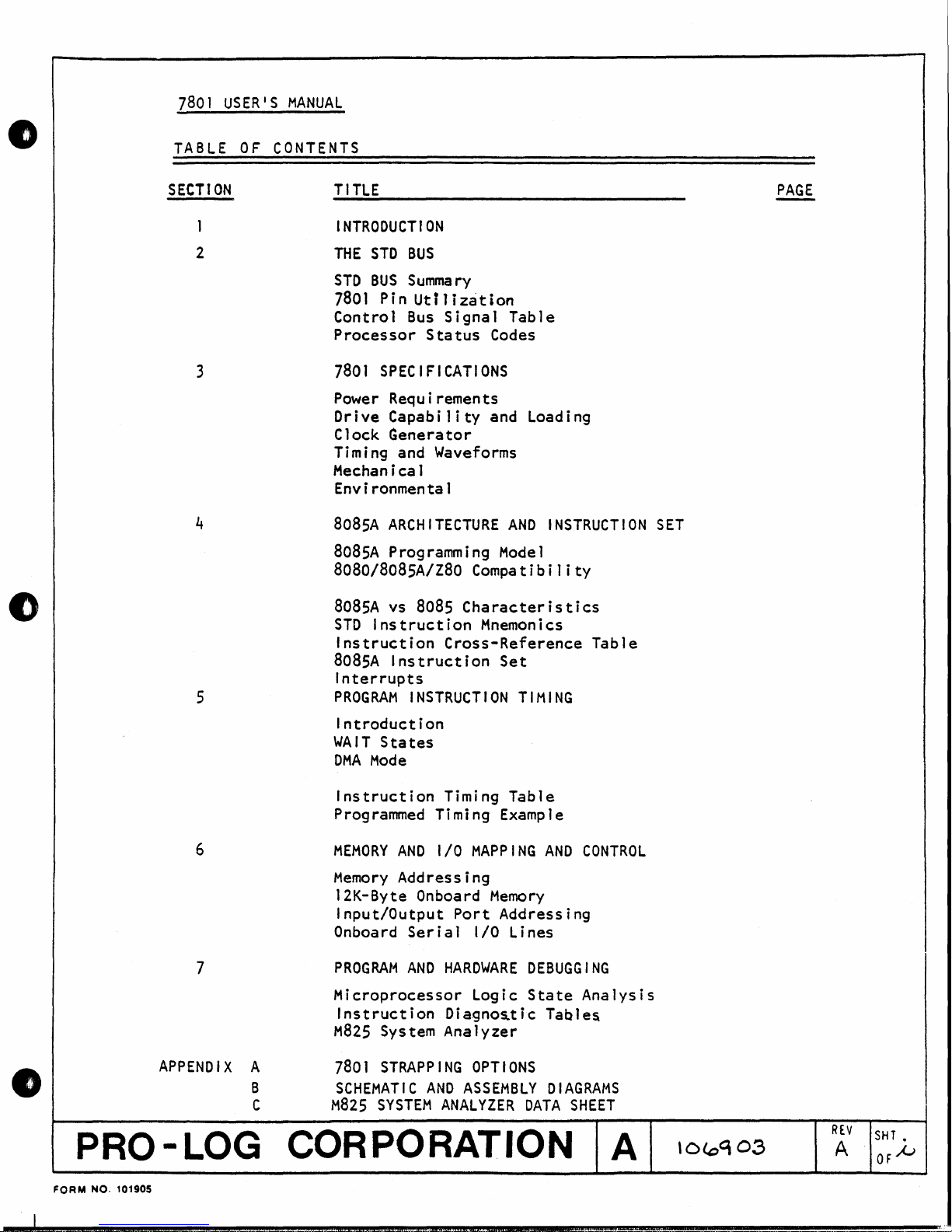
TABLE
SECTION
1
2
3
4
OF
CONTENTS
TITLE
INTRODUCTION
THE
STD
BUS
STD
BUS
Summary
7801
Pin
Ut
i 1 i
za
Bus
Control
Processor
7801
SPECIFICATIONS
Power
Drive
Clock
Timing and
Mechanical
Environmental
80SSA
SOSSA
SOSO/SOSSA/Z80
Requirements
Capability
Generator
ARCHITECTURE
Programming
Signal Table
Status
Waveforms
t ion
Codes
and Loading
AND
INSTRUCTION
Model
Compatibility
PAGE
SET
5
6
7
808SA
STO
Instruction
SOSSA
Interrupts
PROGRAM
Introduction
WAIT
DMA
Instruction
Programmed
MEMORY
Memory
12K-Byte
Input/Output
Onboard
PROGRAM
Microprocessor Logic
Instruction
M82S
vs
S08S
Characteristics
Instruction
Instruction
INSTRUCTION
States
Mode
AND
Addressing
Onboard
Serial
AND
System Analyzer
Mnemonics
Cross-Reference
Timing Table
Timing Example
I/O
MAPPING
Memory
Port
I/O Lines
HARDWARE
Dia9no~tic
Set
Addressing
Table
TIMING
AND
CONTROL
DEBUGGING
State
Analysis
Tables
APPENDIX
A
B
C
•
PRO-LOG
FORM
NO.
101905
CORPORATION
7801
STRAPPING
SCHEMATIC
MS2S
SYSTEM
OPTIONS
AND
ASSEMBLY
ANALYZER
WMiiF
,$liCea:
,,::"U,;===,
DIAGRAMS
DATA
SHEET
_'"x,,;
it
A
"A#II
'Ii
X==';;4M&4NMUiI&iM_
\c<cG\
03
REV
A
SECTION
ONE
PRODUCT
OVERVIEW
I
I
I
I
SOSSA
This card
808SA
PROM sockets.
The
7801
up
to 4K. and sockets
EPROM. An STO BUS system using the
can be expanded to
capability
disabled
PROCESSOR
combines a buffered
microprocessor
includes
The
7801
for
OMA •
withonboard
1 K
byte
for
up
full 808SA
STO BUS interface may be
CARD
and fully expandable
of
RAM
with
to
8K bytes
memory
FEATURES
• 80SSA
• 4096 bytes RAM
• 1024 bytes RAM
• 8192 bytes ROM
• 3 State Address, Data,
Processor
capacity
included
capacity
Control
onboard
(211
4 L
onboard
Buses
type)
(2716
•
• Power-on· reset
• Five
• Serial
•
•
.7801:
interrupts
1/0
All
lC~s.-socket.ct
Single
+5V
6_25
.7801-1:
•
External
or
lines
operation
MHz
6_
144MHz
clock
pushbutton
crystal,
crystal,
input
option
reset
input
320ns time
325.5ns time
RAM and
sockets
of
ROM
7801
card
and I/O':
type)
10
I
for
or
states
states
o
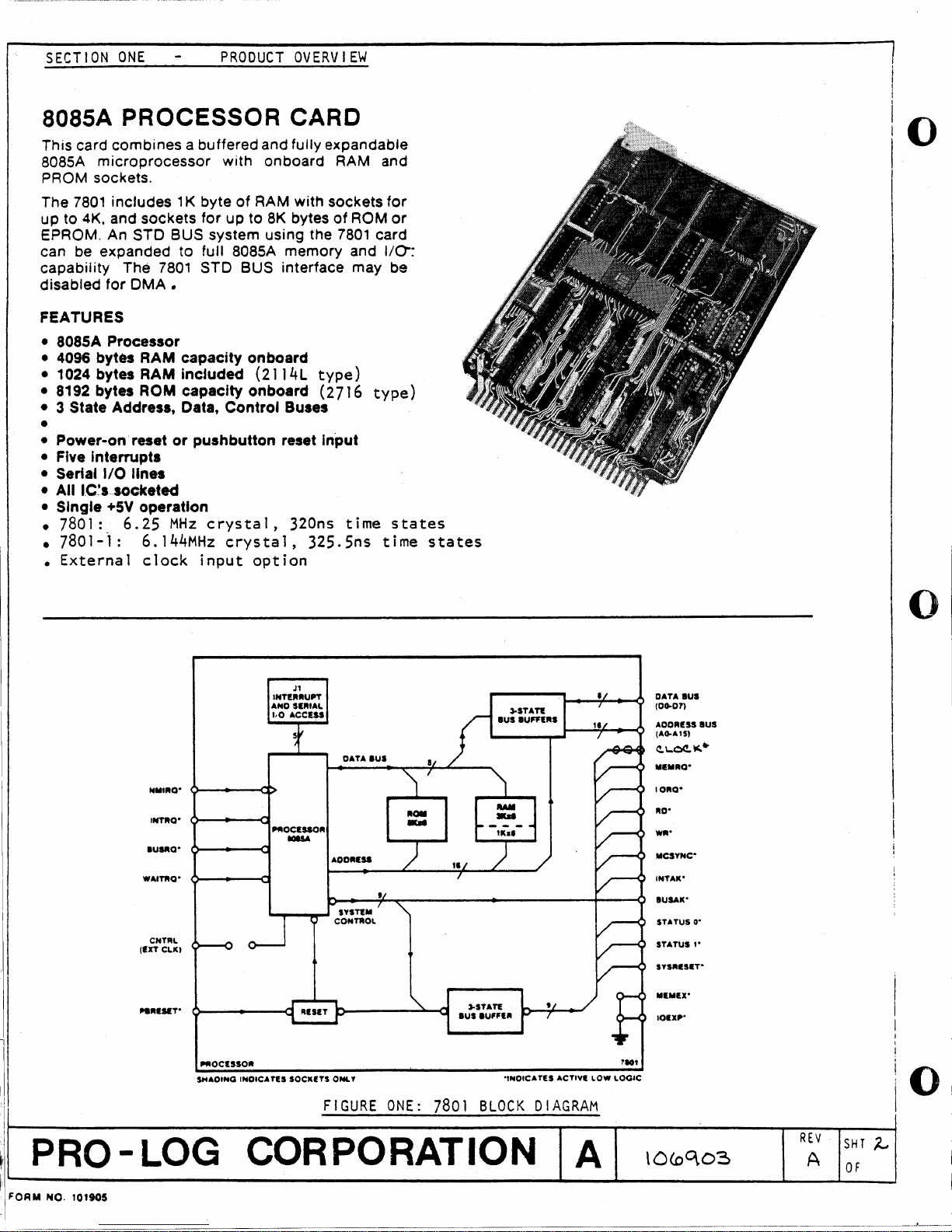
J1
INTIRRUPT
AND SIR.AL.
',0
ACCESS
DATA
IUS
..
M.RO-
INTRa"
IUMO-
WAITRO'
CNTRl.
(IXT CLKI
I
,I
SHADING INOICATIS SOCKETS
I
",OCIISOR
IOI5A
ADORIIS
ONU
FIGURE
ONE:
IUS
7801
IUS
loSTATt
IU"U
'INDICATES ACTIVI
BLOCK
loSTATI
IU,.,'RS
DIAGRAM
,.
LOW
I~----------------------------------------------------------~----~~------~--------~----~----~
II
PRO-LOG
I'II---------------------------'-------~
FOAM
NO. 101905
CORPORATION
A
DATA
IUS
(00007)
AOORISS
IUS
(AOoA1S'
~l..o<!.\IC."
MIMRO-
lORa-
WR'
MCSYNC-
INTAK'
IIUSAIC'
STATUS
O'
STATUS
l'
STSRn_TO
M'MlX'
10UIt·
7101
l.OGIC
REV
A
_
_L_
SHT
OF
_
'),.,
__l

o
SECTION
The
microprocessor
The
cards,
to
to
a bussed motherboard
As
for
TWO -THE
STO
BUS
standardizes
STO
BUS
the
the
with
app1
all
ication.
system
maintaining
card
is
dedicated
external
processor
the
STO
BUS
the
physical
systems,
providing a dedicated,
to
internal
communication
The
standardized
that
allows
and primary system
signal
functionality
and
electrical
aspects
orderly
communication and power
made
via
I/O
connectors
any
pinout
card
and
to
control
defined
56-pin
work in any
card,
by
the
STO
of
modular
interconnect
distribution
which
connector
slot.
the
7801
BUS
standard.
a-bit
are
lends
is
responsible
scheme.
between
suitable
itself
A complete copy
TECHNICAL
California
STO
BUS
The
56-pin
Figure
and
signal
LOGIC
POWER
BUS
DATA
BUS
MANUAL,
93940.
Summary
STO
, shows
flow
PIN
MNEMONIC
1
3
5
7
9
11
13
of
the
available
BUS
is
1.
2.
3.
4.
5.
the
relative
·SV
G~O
-5V
03
02
01
DO
STO
BUS
standard
from Pro
organized
Logic Power
Oata
Address
Control
Aux
Bus
Bus
Bus
i 1 a ry Power
organization
to
the
COMPONENT
SIGNAL
FLOW
In
In Digital
InlOut
InlOut
InlOut
InlOut
SIDE
+S
-S
Volts DC
Low
Low
Low
Low
is
contained
Log
Corporation,
into
five
Bus
and
7801
Volts
Processor
DESCRIPTION PIN
DC
(Bussed)
Ground
Order Data Bus
Order
Data Bus
Order
Data Bus
Order
Data Bus
functional
pins
pins
pins
pins
pins
pinout
(Bussed)
1-6
7-14
15-30
31-52
53-56
of
the
card:
MNEMONIC
2
4
6
8
10
12
14
in
2411
groups
STO
BUS
·SV
GNO
-5V
07
06
OS
04
the
SERIES
7000
STO
Garden Road, Monterey,
of
with
CIRCUIT
SIGNAL
FLOW
In
In
InlOut
InlOut
InlOut
InlOut
backplane
mnemonic
SIDE
·S
Volts
Digital
-5 Volts DC
High
High
High
High
signals:
function
DESCRIPTION
DC
Bussed)
Grol.;~C
Order
::Ja:a
Order
Ca:a Bus
Order
Cata Bus
Order
Ca~a
BUS
Bussed)
Bus
Bus
15
17
19
ADDRESS
BUS
CONTROL
BUS
•
FORM
NO. 101905
: t
AM#.
WM¥4#¥W
·Low
POWER
BUS
L.evet
21
23
25
27
29
31
33
35
37
39
41
43
45
47
49
51
53
55
Active
Indicator
AMMM4¥AN4¢4fTM
A7
A6
AS
A4
A3
A2
Al
AO
WR·
lORa·
10EXp·
REFRESH·
STATUS
WAITRO" In
SYSRESET"
AUXGNO
BUSAK"
INTAKo
CLOCK"
peo
AUX+V
1·
P¥
gp4M¥4QM44¢
Out
Out
Out
Out
Out
Out
Out
Out
Out
Out
Out
Out
Out
Out
Out
Out
Out
Low
Order
Low
Order
Low
Order
Low
Order
Low Order Address Bus
Low
Order
Low
Order Address Bus
Low Order Address Bus
Write to
I/O
110
Refresh
CPU Status
Bus
Interrupt
Walt ReQuest
System Reset
Clock
Priority Chain
AUX
AUX POSitive
AA
4M4hP4\#¥4#MMii#
Memory
Address Select
ExpanSion
Timing
Acknowledge
Acknowledge
from Processor 50
Ground
Wf#4¥MA
Address Bus
Address Bus
Address Bus
Address Bus
Address Bus
or
I/O
'.
Out
(BUSSed)
(-12
Volts DC)
_-2.---:
16
18
20
22
24
26
28
30
32
34
36
38
40
42
44
46
48
52
54
56
A15
Al
..
A13
A12
All
A10
A9
A8
RD·
MEMROMEMEX·
MCSYNC·
STATUS
BUSRO·
INTRO"
NMIRO'
PBRESET'
CNTRl·
PCI
AUXGND
AUX-V
4T\
A
A¥4A
Out
Out
Out
Out
Out
Out
Out
Out
Out
Out
'Out
Out
O·
Out
In
In
In
In
In
In
-rl\l.
\O~~
AWPW¥M4P4%?44I
High
Order
High
High
High
High
High
High
High
Read to
Memory Address Select
Memory ExpanSIon
CPU MaChIne
CPU Status
Bus ReQuest
Interrupt ReOuest
Non-MaskaOI~
Push Button
AUX TimIng
PriorIty Cha,'"
AUX
AUX NegatIve
Srp
WM,
A-:dress
Order
Ao:lo:lress
Order
AIjClress
Order AOdress Bus
Order Address Bus
Order
Address Bus
Order
Address Bus
Order
Adljress
Memory
Grouna
~U
A%#i,4
Cycle
~eset
In
8'.Jssea)
-'2
P#
4%4
or
I nterru pt
Volts
S
P P
Bus
Bus
Bus
Bus
I.
0
Sync
#4
DC,
4 r
STO
BUS
Pin
Utilization
by
7801
Since
pins
of
capability.,
The
1. Logic Power Bus:
2. Data Bus:
the
STO
be
used,
the
microprocessor
its
8085A
allocation
power
shown
peripheral
memory
With
direction
signal
high
by
Data Bus.;
Data
to
in
sockets,
the
outputs~
impedance
the
7801. Note
Bus
BUS
the
microprocessor,
The
b~ffers
of
the
7801.
Pins
Figure
cards
exception
of
data
AO-A7
when
BUSAK*
standard
timing
type
decrease
STO
BUS
+5V
Pins
7 through
2 High
over
this
data
of
flow
Peripheral
state
except
that
appear
is
does
and
signal
used.
with
lines
(pins
5 and 6
14
this
also
Direct
with
the
on
00-07
active
not
specify
allocation
The
LSTTL
memory
for
the
1,2)
and Logic Ground
are
form an
level
bus.
cards
when
active
When
appears
Memory
its
I1EHRQ,r"
addressed
low-order
while
in
response
timing
assumes
characteristics
buffering
and I/O
7801
open.
8-bit
Access
are
is
bidirectional
data
the
7801
on
the
(DMA)
10RQi"
required
and
address
MCSYNC*
to
or
require
many
of
of
the
added
access
given
flows between
fetches
STD
RD""
to
directed
bits
is
BUSRQ*,
to
enhance
time
below.
(Pins
Data Bus.
operations,
release
active.
3,4)
data
WR'':,
and
to
(AO-A7)
as
in
3-state
that
the
7801
are
slightly.
supply
the
7801
from
the
INTAK~r,
the
data
drive
are
multiplexed
The
7801
DMA
operations.
all
available
characteristics
dictated
the
card's
operating
data
and
its
onboard
7801
control
bus
the'data
releases
bus
controls
to
by
drive
as
its
the
bus
on
o
the
the
the
3.
Address Bus:
Figure
these
1
ines
The
7801
as
in
4.
Control
interrupt,
signals
The
7801
for
the
5.
Auxilary
electrically
The
7801'
timing
information
Pins
2 . The
lines,
(AO
DMA
and shows
meets
and
through
releases
operations.
Bus:
following
Pins
and fundamental
releases
Power Bus:
openc
all
15
through
7801
8-bit
of
and
drives
I/O
A7
on
the
Address
31
through
how
they
the
Control
output
Pins
the
signal
specifications
port
pins
system
are
signals:
53
through
30
form a
high
level
addresses
15, 17, 19, 21, 23, 25,
Bus
when
52
provide
operations.
derived
Bus
during
MEHEX,;',,
requirements
56
are
l6-bit
active
over
BUSAK*
control
from
are
8085A
BUSAK*
10EXPi"
not
of
in
Section
3-state
l6-bit
the
is
active
signals
Figure
signals.
in
used
the
STD
3.
address
memory
eight
response
BUSAK;'"
by
low-order
27
and
in
for
3 summarizes
the
BUS
standard.
bus
as
addresses
address
29).
response
memory, I/O,
to
CLOCK'~',
7801
to
these
BUSRQ*,
PCO.
and
are
Detailed
shown in
over
BUSRQ~~,
except
o
I
PRO-LOG
FORM
NO. 101905
CORPORATION
A
REV
A
SH
OF
o
T
"-f
e
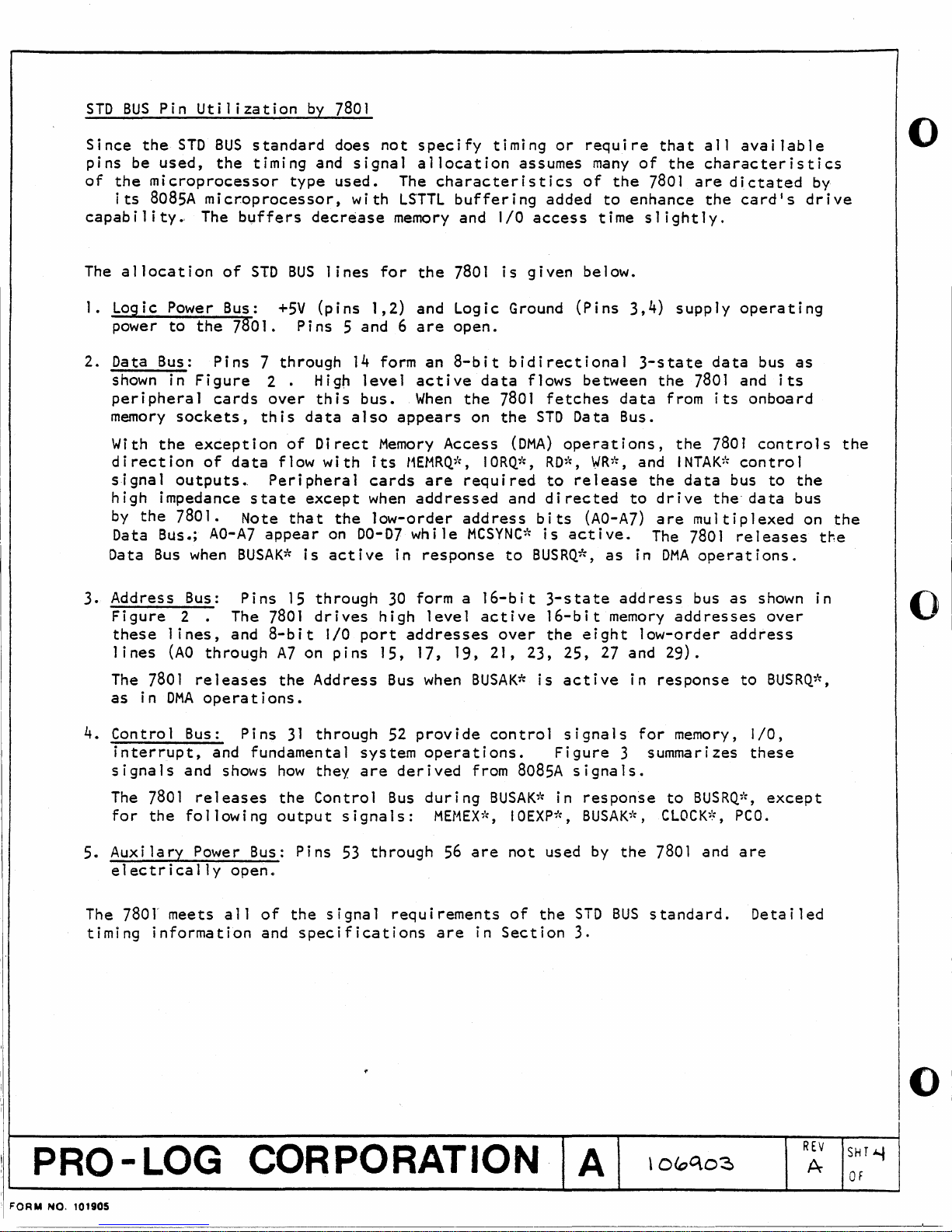
:MNEMOt-J
iWR
:RD*
I C
!
I
IORQ1
MEMRQ";
I
i
I
10EXP*
MEMEX*
REFRESH~':
MCSYNCr;
PIN
31
32
33
34
35
36
37
38
IN/OUT
Out#
Out#
OUT#
OUT#
OUT
OUT
-
OUT#
FUNCTION
Write
Read
from
AO-A7
AO-A15
address
I/O
expans~on
Memory
:
One
(Not used)
transition
cycle;
to
memory
memory
hold
valid
hold
valid
expansion
undecoded
or
I/O
or
I/O
memory
control
control
per
machine
I/O
address
status
IHOW
I
[WR1;]
DERIVED,
808SA
[RD*]
[IO/M*]*
[IO/M*]
,
User-removabl~
User-removable
I E 1 ec t
[ALE]
rica
*
1 1 y
ground
open
NAME
ground
e
STATUS
STATUS
BUSAK*
1*
..
0".
I
:
I
;BUSRQ*
!
i I
NTAKr~
:
i
i
IINTRQ*
WAITRQ*
NMIRQ*
SYSRESET~':
PBRESET~I;
CLOCK;':
,-
CNTRL~';
i
IPC I /PCO
!
I
!
39
40
41
42
43
44
45
46
47
48
49
50
52/51
OUT#
OUT#
OUT
IN
Undecoded
ndecoded
Acknowledges
Bus
.
!
;
OUT# ! Acknow
:
:
IN
IN
IN
OUT#
IN
OUT
IN
IN/OUT
Maskable
Synchronous
Nonmaskab1e
System power-on and pushbutton
Pushbutton
Time
External
Priority
status;
status,
BUSRQ*
request
processor
driver
1 edges I
(DMA);
halt
disable
NTRQ*
(MEMRQ* . RD*)
interrupt
vector
interrupt
processor
interrupt
reset
one-shot
reset
State
tlock
frequency)
clock
Time
State
Clock frequency)
chain
Note
Note
synchronous I
and
3-state
and rep 1
to
read
request
ha
request
output
input
( 1
/2
cry s ta
input
(2
1
1
1 t
times
[S
1]
*
[SO]
*
i
[HLDA]
[HOLD]*
l
I
ace~[
1
I
NTA;'~]
[I
NTR]'':
[ROll
~
j
[TRAP]
;[RST]*
I
:[R~':
]
I
[CLOCK]
i jumper
-
:~1
1
--i
INote
user
connection
~
*
1;
.....
-
* -
--
optional
...
----
.
..---
user
optional
connection
jumper
-
~
*
#
[]
NOTES:
FIGURE
PRO-LOG
~nA'"
Nn
tOtQOS
3
CORPORATION
- ,enM4==4I
Low
1 eve 1
Output
buffer
Denotes
See
t.
2. Trace
maintain
:
7801
"i.
t"";
active
disabled
equivalent
Figure
on
4
7801
chain
CONTROL
" j,,.ij
IW
W
Bo8SA
for
status
connects
continuity.
BUS
SIGNALS
when
signal
PCI
BUSAK*
active
name
information.
to
PCO
to
A
\OCDq,O~
:UM
4$
M , Mg., 4
REV
SHT
S
A
OF
p;;
......
1,'4

7801
Processor
MCSYNC*,
which
displaying
certain
The use
device-type
STATUS
is
peculiar
peripheral
of
Status:
0*,
and
to
processor
chips
these
signals
independence
MCSYNC*,
STATVS
the
808SA
status
and
is
is a design
STATUS
1*
signals
microprocessor.
in
logic
systems
not
sign~l
designed
recommended in
goal.
0*,
STATUS
provide
analyzers,
1*
encoded
These
to
work
systems
Signals
status
signals
and can be used
with
the
where
information
are
useful
808SA
microprocessor
for
to
drive
specifically.
o
SEE
2
MCSYNC*
of
a machine
logic
instruction
The
lagging
address
address
data
of
MCSYNC*
MCSYNC*
STATUS
machine
NOTE
I
I
I
serves
signal
is
lines
in
subseq~ent
is
0*
and
cycle
MACHINE
Read
Read
memory
Wr i te
Acknowledge
Acknowl
interrupts
Bus
idle
to
H,L
a dual
cycle
analyzer
for
analysis.
edge
present
(AO-A7)
is
used
equivalent
STATUS
in
instruction
in
memory
edge
during
pair)
function.
(Section
to
select
of
MCSYNC*
on
the
during
time
states
on
the
to
the
1",
can be decoded
progress
CYCLE
except
INTRQ*
NM I RQ":
S.5,6.5,7.5
TYPE
opcode 0
opcode 1
and
ADP
(Add
instruction
3
occurs
sro
time
7801
80SSA's
as
shown in
Its
leading
).
Counting
a
specific
when a stable
Data Bus.
state
within
to
latch
ALE
:STATUS
o
o
o
edge
denotes
the
MCSYNC*
machine
The
808SA
TI;
-tne
the
machine
thp
low
(Address Latch Enable)
externa
Figure
0*
4:
STATUS
cycle
memory
device
address
~ycle.
order
11 y to i dent
address.
I'~
,MEMRQ'"
o
o
I 0 I 1 j 0 I 1 I 1
o
a
o
o
o
the
approximate
transitions
within a mUlti-cycle
line
address
mu1.tiplexes
information
The
lagging
i fy
the
I ORQi;!
allows
output
type
RDi, ; It/R,'t
I
i
1
1
or
I/O
jots
is
followed
(rising)
signal.
of
o I
o
o
1,
!
i
I
start
a
port
low
\ I
order
by
edge
NTAKi:
o
o
I.
2.
3.
4.
HALT
The
those
states
The Data
for
generated
Processor
Timing
For
3
NOTES:
PRO-LOG
FORM
NO. 101905
instruction
FIGURE
states
the
additional
shown
produced
are
reversed.
Bus
ADP
during
pins
for
STATUS
4:
MACHINE
for
by
the
is
idle
ins t ruc
t ion (I rrte 1
these
10/M*,
0*
information,
CORPORATION
CYCLE
MEMRQ":
808SA
during
cycles.
RD*,
WR*
and
STATUS
STATUS
and
fORQi,
dev
ice.
the
second and
mnemon i cis
((808SA
are
1*
refer
SIGNALS
during
For
in
is
similar
to
the
the
only).
the
808SA
*low
interrupt
ea r
lie
third
DAD).
high
machine
impedance
to
Address
manufacturer's
A
active:
acknowledge
r 8085,
No
MCSYNC*
o
Active
Inactive
the
MEMRQi:
cycles
state.
Bus
\o~qo~
machine
CAlE~")
timing
literature.
I
= a
= 1
cycles
and
cycles
signa 1 is
(Section
REV
A
are
10RQ":
3).
SH
T
OF
o
I.p
o
SECTION
Power Requirements
3 -
7801
SPECIFICATIONS
•
!
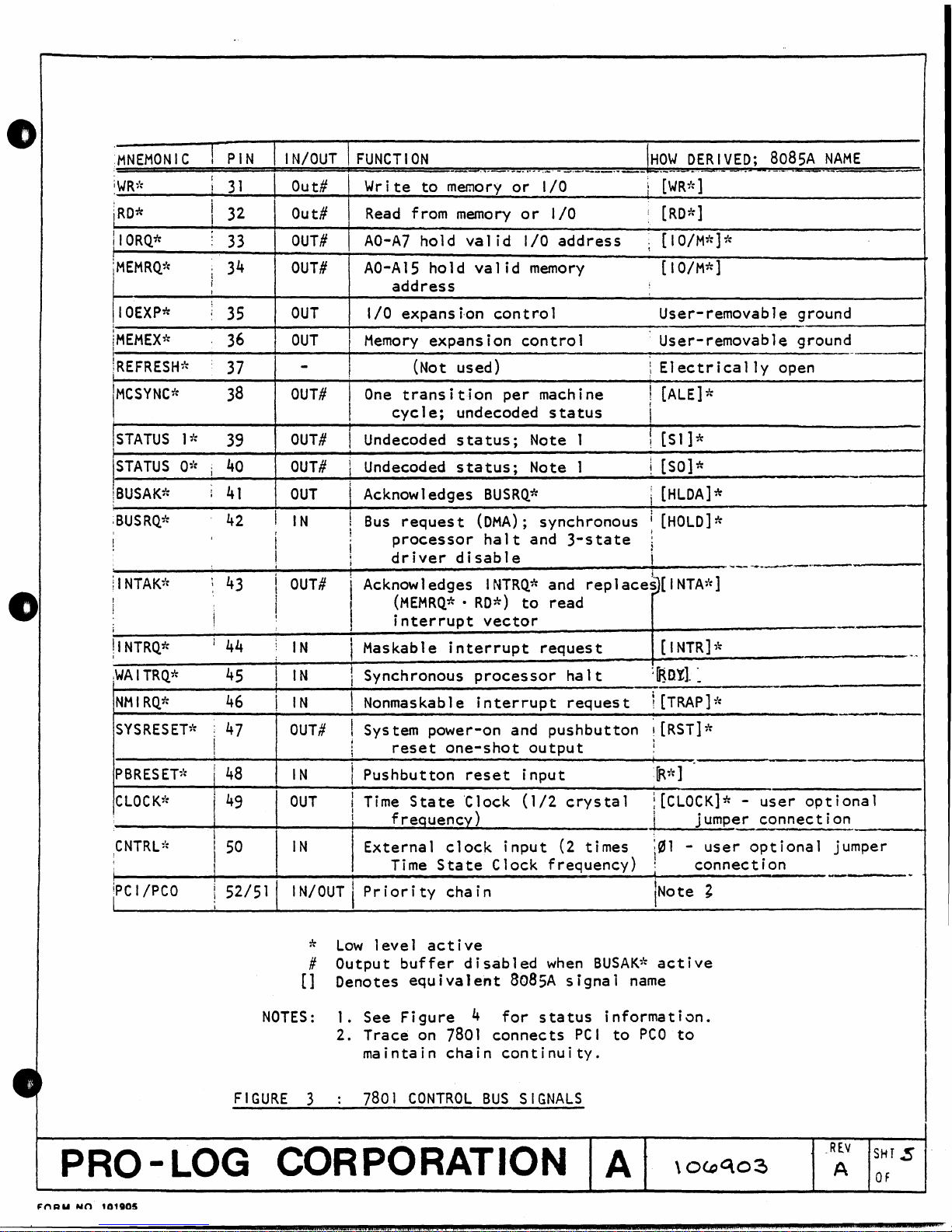
RECOMMENDED
PARAMETER
Vcc
lice
Both
the
power-on
reset
less
one-shot
than
(Note
(Note
NOTES:
8085A
for
and 2114L
stabilization
provides
10
milliseconds.
OPERATING
I
MIN
1)
4.75
2)
:
FIGURE
1.
In
following
2. Icc
RAM
75
for
LIMITS
TVP
11.00
order
a.
+0.50
b.
+0.50
specification
sockets
rnA
each
devices
of
adequate
I
5.00 5.25
5:
7801
to
power
Vcc
rise
less.
If
Vcc
time
it
specified
per
device
internal
ABSOLUTE
i
MAX
I
1.40
guarantee
Volt
drops
must be
Volt
on
2716
require
stabilization
I
POWER
must be monotonic,
operating
the
SUPPLY
supply
to
+4.75
below
before
assumes
7801
EPROM
not
used.
10
bias
correct
considerations
Volts
+4.75
returned
restoration
are
and
milliseconds
oscillators.
delay,
NONOPERATING
MIN
0
!
SPECIFICATION
operation,
rising
in
10
Volts
to
less
range.
that
all
loaded.
SOmA
(typical
per
values)
only
MAX
5.50
to
EPROM
minimum
I
!
!
apply:
from
ms
or
at
any
than
the
and
Subtract
2114L
The
780l's
if
Vcc
UNITS
Volts
Ampere
the
RAM
after
risetime
LIMITS
initial
power-on
I
I
,
I
f
i
i
is
Drive
The
Interrupt
in
In
(one
a
are
Exceptions
•
PRO-LOG
FORM
NO. 101905
Capability
780)IS
LSTTL
general,
LSTTL
minimum
electrically
STD
Socket
loads
input
or
of
50
to·
and Loading
BUS
Jl
as
defined
lines
MOS
input
LSTIL
open.
the
general
a.
WAITRQ*
b.
PBRESET*
parallel
c.
CLOCK*
d.
PCI
else
CORPORATION
Edge
(Figure
loads.
and
on
Connector
7 )
give
by
the
SERIES
and
disabled
plus
4.7K
Pins
loading
input,
input,
with 2 LSTTL
output,
PCO,
the
which
which
which can
which
7801.
Pin
List
input
3-state
pullup
which
rules
is
are
(Figure
loading
7000
TECHNICAL
outputs
resistor).
are
unspecified
are:
15
LSTTL
is 1 uF
loads
•
drive
connected
6 ) and
and
loads.
typical
10
LSTTL
to
A
Serial
output
MANUAL.
present 5 LSTIL
Output 1
in
in
loads.
each
other
drive
ines
Figures
but
can
I/O and
capability
loads
drive
6 and 7
to
nothing
maximum
REV
SHT
A
OF
i
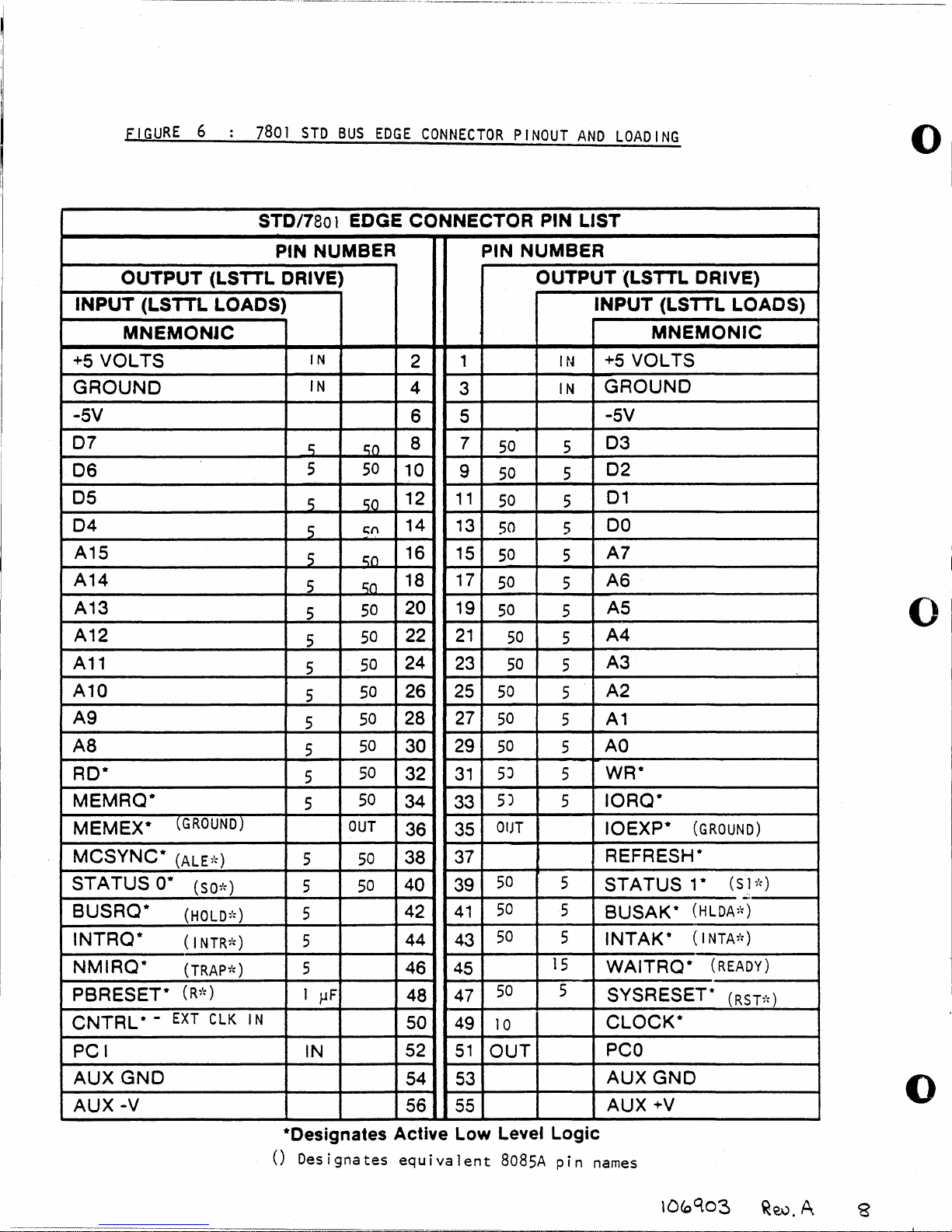
FIGURE
6
7801
STD
BUS
EDGE
STD/7801 EDGE CONNECTOR PIN LIST
CONNECTOR
PINOUT
AND
LOADING
o
OUTPUT
INPUT
+5
(LSTTL LOADS) INPUT (LSTTL LOADS)
MNEMONJC
VOLTS
GROUND
-5V
D7
D6
D5
D4
A15
A14
A13
A12
A11
A10
A9
A8
RD*
MEMRO*
MEMEX*
MCSYNC*
STATUS
O·
BUSRO*
INTRO*
NMIRO·
PBRESET*
CNTAl * -
PCI
PIN
(LSTTL
(GROUND)
(ALE~~)
(SOi: )
(HOLD;':)
(I
NTRi:) 5
(TRAPi: ) 5
(R;':)
EXT
eLK IN
NUMBER
DRIVE)
IN
IN
s
5
5
5
5 'iO
5
5
5
5
5
5
5
5
5
5
5
5
1
iJF
IN
'iO
50
so
c;n
'in
50
50
50
50
50
50
50
50
OUT
50
50
2
4
6 5
8 7
10
12
14
16
18
20
22
24
26
28
30
32
34
36
38
40
42
44
46
48
50
52
PIN NUMBER
OUTPUT :(LSTTL DRIVE)
1
3
50
9
50
11
50
13
50
15
50
17
50
19
50
21
23
25
27
29
31
33
35
50
50
50
50
50
5J
5)
OUT
37
50
39
50
41
50
43
45
50
47
49
10
51
OUT
IN
IN
5
5
5
15
5
+5
GROUND
-5V
D3
5
02
5
01
5
DO
5
A7
5
A6
5
A5
5
A4
5
A3
5
A2
5
A1
5
AO
5
WR*
5
IORO*
5
IOEXP*
REFRESH*
STATUS
BUSAK*
INTAK*
WAITAO*
SYSRESET*
ClOCK*
PCO
MNEMONIC
VOLTS
(GROUND)
1·
(HLDAi':)
(INTAi:)
(READY)
o
(S 1 ;':)
-.
(RST;':)
AUX
GND
AUX-V
*Designates Active
()
Designates
54
56
equivalent
53
55
Low
Level
8085A
Logic
pin
AUX
AUX
names
GND
+V
o
•
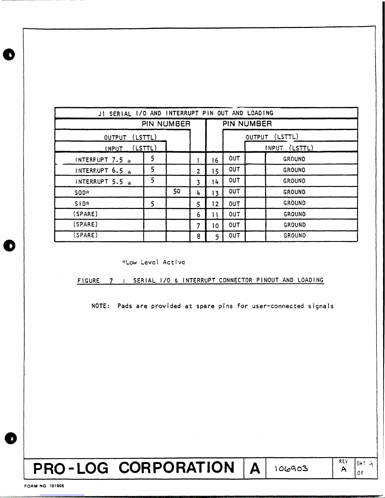
Jl
SERIAL
I/O
PIN
AND
INTERRUPT
NUMBER
PIN
OUT
AND
LOADING
PIN NUMBER
e
~
OUTPUT
I
INTERFUPT
I
NTERF'.UPT
INTERRUPT
SOD":
SID":
(SPARE)
(SPARE)
(SPARE)
FIGURE
NOTE:
NPUI_
7.5
6.5
5.5
*Low
7 :
Pads
(
LSTTL)
(LSTTL)
*
*
*
Level
SERIAL
are
5
5
5
50
5
Active
I/O & INTERRUPT
provided
at
1
2
3
4·
5
6 1 1
7
8
spare
OUT
16
OUT
15
OUT
14
OUT
13
OUT
12
OUT
OUT
10
OUT
9
CONNECTOR
pins
for
OUTPUT
user-connected
.(
LSTTL)
INPUT
PINOUT
GROUND
GROUND
GROUND
GROUND
GROUND
GROUND
GROUND
GROUND
AND
(LSTTL)
LOADING
signals
•
PRO-LOG
FORM
NO. 101905
CORPORATION
.=
____ " ..
*
__
":.45:::",,;
l6.,ml:I,#'
A
#.$
4T4¥
REV
SH
r:..,
A
OF
$
AlMA ( ",iLk
It
.-
Clock
The
the
divided
is
execution
(see
The
period.
of
If
with
are
or
Generator
7801
's
primary
by
the
shortest
Section
7801
is
The
th i s
crys
desired,
a TTL-compatible
given
external
!
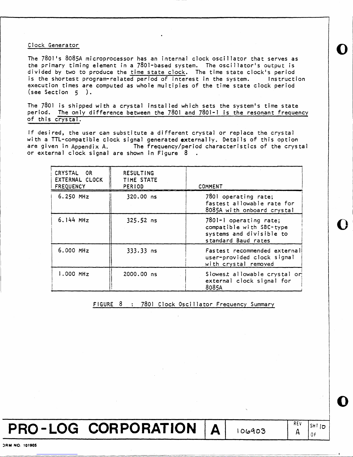
CRYSTAL
i
EXTERNAL
FREQUENCY
I
6.250
!
6.144
i
I
6.000
1.000
i
8085A
two
times
in
microprocessor
timing
to
produce
program-related
are
5
).
shipped
only
difference
ta
1 •
the
user
Append~x
clock
signal
OR
CLOCK
MHz
MHz
MHz
MHz
element
computed
with a crystal
can
clock
A.
in a
the
as
between
substitute
signal
are
shown
RESULTING
TIME
PERIOD
I
j
320.00
time
I
325.52 ns
333.33
2000.00 ns
I
j
!
has an
7801-based
period
whole
The
STATE
internal
state
installed
a
generated
frequency/period
in
clock.
of
multiples
the
7801
different
Figure
ns
ns
clock
system.
interest
of
which
and 7801-1
crystal
externally.
8
I
,
I
,
I
I
I
j
I
oscillator
The
oscillator's
The time
in
the
the
time
sets
COMMENT
the
is
or
Details
characteristics
7801
operating
fastest
8085A
7801-1
compatible
systems
standard
Fastest
user-provided
wi
th
crys
SlowesX
external
8085A
that
state
system.
with
operating
clock's
state
system's
the
resonant
replace
of
allowable
onboard
with
and
divisible
Baud
recommended
ta
1 removed
allowable
clock
serves
output
Instruction
clock
time
the
crystal
this
of
rate;
rate
crystal
rate;
SBC-type
rates
clock
crystal
signal
as
is
period
period
state
frequency
option
the
crystal
for
to
externall
signal
for
or:
I
I
!
i
I
I
I
I
I
I
!
,
o
o
FIGURE
PRO-LOG
::lRM NO. 101905
CORPORATION
8
7801
Clock
Oscillator
Freguency
A
Summary
"
\0<0'\03
REV
A
SHT
OF
o
ID
e
0
Timing
An
for
other
7801-based
The
with
by
Figure
Specifications
understanding
the
selection
peripheral
7801
's
add
it
the
7801
9.
of
STO
STD
BUS
timing
i ona 1 de 1
and
the
SIGNALS
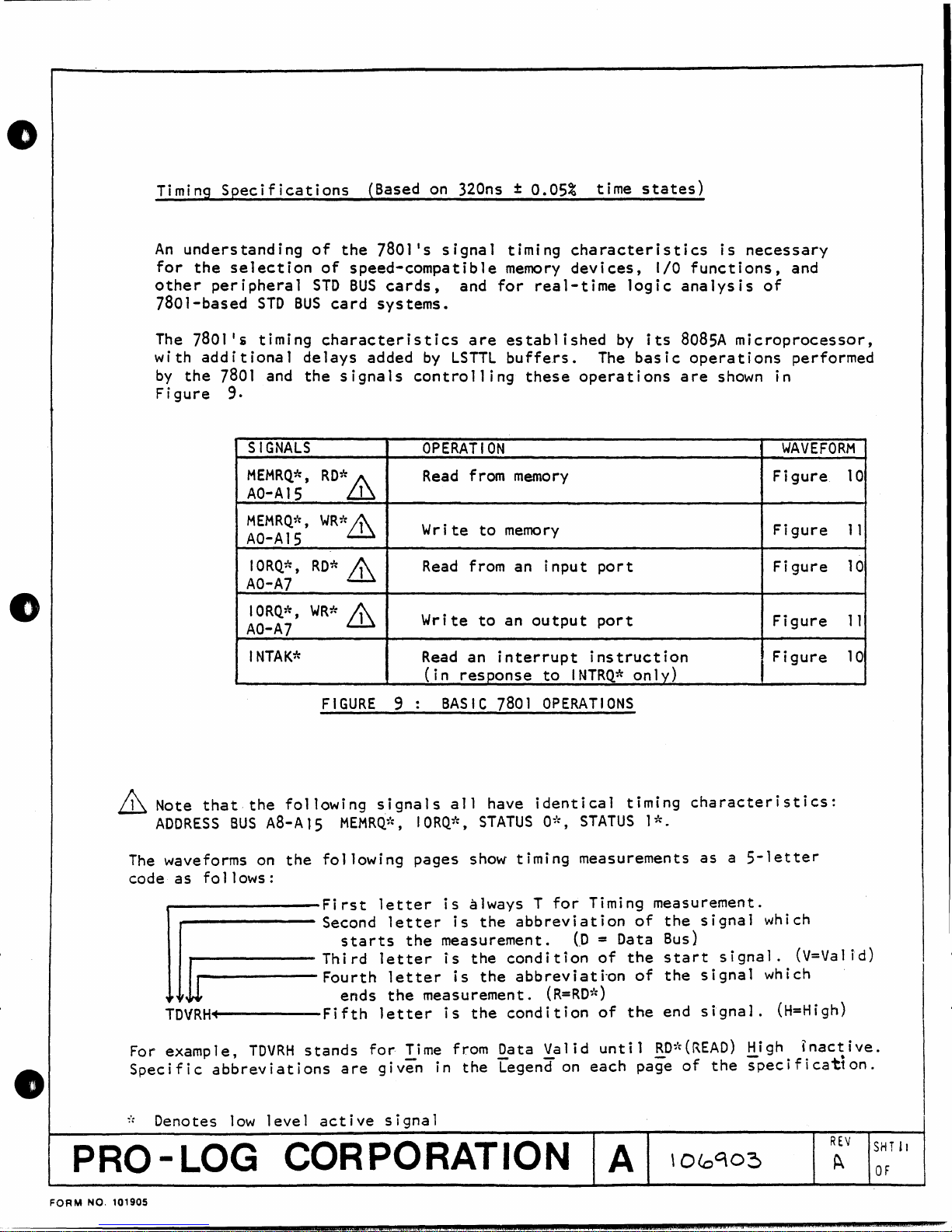
MEMRQ*,
AO-Al5
MEMRQ1:
AO-A15
10RQ*,
AO-A7
10RQ*,
AO-A7
,
RD*
WR*
(Based
the
7801's
of
speed-compatible
BUS
cards,
card
characteristics
ays
RD*&
WR*,&
systems.
added
signals
.&
.&
by
controlling
OPERATION
Read
Write
Read
Write
on
320ns ± 0.05% time
signal
and
LSTTL
timing
memory
for
are
established
bu
from
memory
to
memory
from an
to
an
real-time
ffe.rs.
these
input
output
states)
characteristics
devices,
The
operations
port
port
logic
by
bas i c
I/O
its
is
necessary
functions,
analysis
808SA
are
microprocessor,
opera t ions
shown
and
of
performed
in
WAVEFORM
Figure
Figure
Figure
Figure
10
11
10
11
.&
Note
ADDRESS
The
waveforms
code
as
__
-------------First
-------------
---------
Ir
,
,U
TOVRH+4-----Fifth
For example,
Specific
I
NTAK*
that·
the
fa
BUS
A8-A
on
the
follows:
rDVRH
abbreviations
FIGURE
110wi
ng
signa 1 s. a 11
15
MEMRQ~':,
following
letter
Second
starts
Third
Fourth
stands
ends
for·
are
letter
letter
given
Read
(in
:
9
letter
letter
the
BASIC
I
ORQ*,
pages show
is
is
the
measurement. (0 = Data Bus)
is
is
measurement.
is
lime
from
in
an
interrupt
response
7801
have i
STATUS
timing
always T
the
abbreviation
the
condition
the
abbreviati"on
the
condition
.Q.ata
the
Legend
instruction
to
INTRQ*
OPERATIONS
dent
i ca I t
O~':,
STATUS 1 *.
measurements
for
(R=RD~':)
y'alid
on
only)
imi
ng
character i st i cs:
as a 5-1etter
Timing measurement.
of
the
signal
of
the
start
of
the
signal
of
the
end
signal.
until
each
~D~':(READ)
page
of
Figure
which
signal.
which
High
the
specificat1on
(V=Val
(H=High)
inactive.
10
id)
.
•
PRO-LOG
FORM
* Denotes
NO. 101905
low
level
active
CORPORATION
signal
t I I
",4R i 4i#A4
4A4
lap
,m
A
tt¥A4lAM
.•
' iA;a; I
REV
SH T II
~
OF
II
'- ; $\4
M.
Q.«
Ii;
..
$.,.
iMwur
CLCG~*
:'
r""~~("r-
f"'r..,-.,; \ -.....
,:..:';
-A:!,
.'vl
= i\'\
::.~
:.;:
~:~
::
.' •
....,;'~
~...
..
....
-"
.J
r.
.....
.
" -
....
__
.J
~:;:
7
I~
.:.'
~r
~(~
.,!.'
~~
.
.
to!
,.
I_
I
I
!
J
__
t
-~.:
J
I,
I
'j
\"
VAL.l
•
Ao-.47
T1
\
,..\t!>
~',.
!)
T~L.l:>~
0(..1;-
.::-
-sa-;4-
,V\AC~
I
j
/
,
::-:~1
z,y
I
___
..
i
i
I
*
t--.
c,ycLE..-·
(,'JE..
TZ-
\
\
_._
~RL
II~
T~l.DV
..
-'--'--'
-
I
,
,
..
....
;...
_-
...
_----
1
,
!
I
\
~
...
(
pAr.to.
.,I
T3
\
\
-
I---
.
I
!
51
I:
-.1
1...-
..... I
",
~L
I
(~
,.--t
~!
J
)
i
/
---
--"/
-+
T~HM-
~/.·
~!
-I-
(
..
:-.
/1\
I
o
71
\
\
-
I
---
•
I
\
L:2GEND
Any
A
j
I
~.
I
;0
(
I
:R
:l
H
:v
iZ
I
I
E~RQ'-:
Any
1 i ne
RD":
low
High
Va
High
imEedance
NOTE:
Address
AO-~~t;
,I
~db':
Data
00-07
1 i ne
state
state
lid
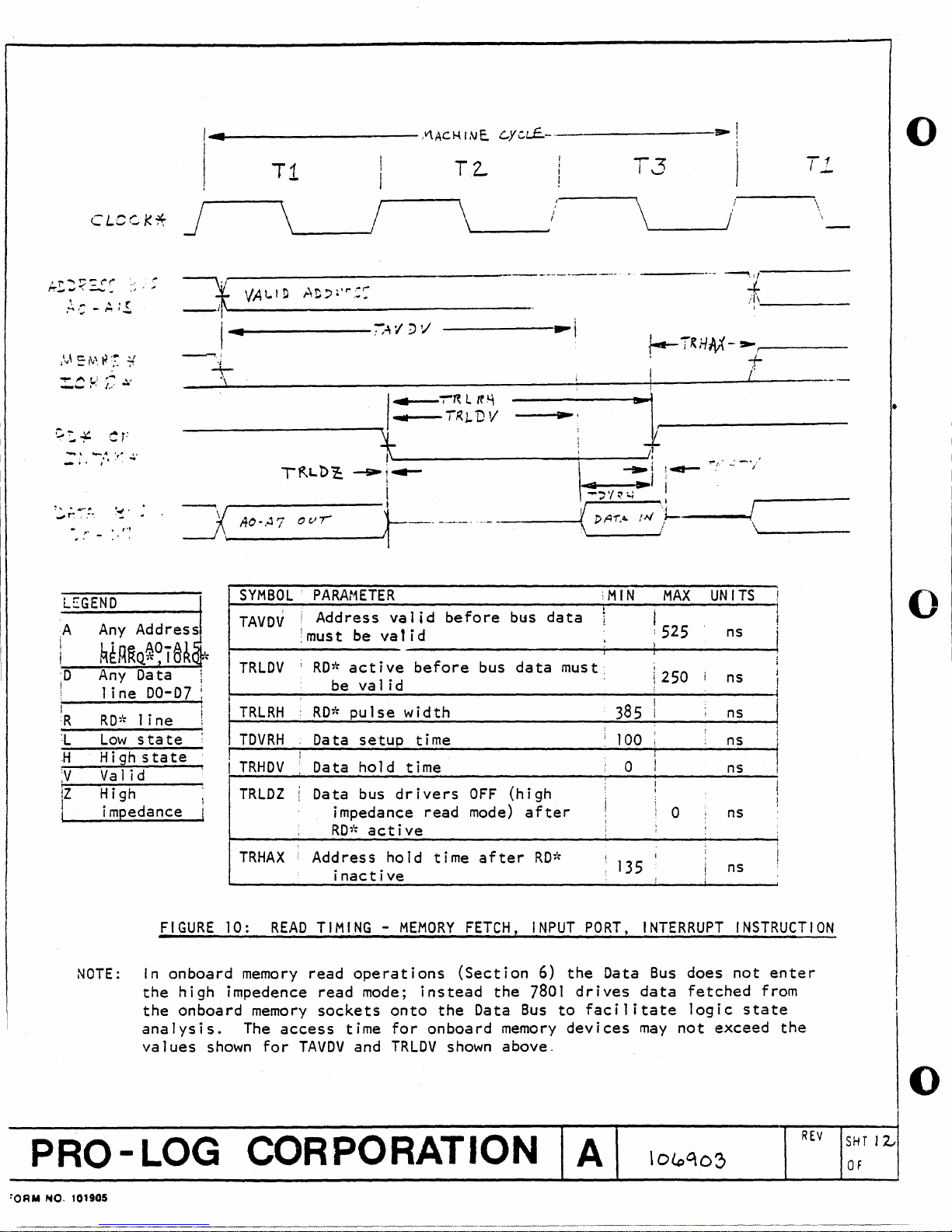
FIGURE
In
onboard
the
high
the
onboard
analysis.
values
SYMBOL'
TAVDV
TRlDV
i
I
I
,
I
I
TRlRH
\
TDVRH
!
TRHDV
I
; ,
TRlDZ , Data
\
i
TRHAX
10:
memory
impedence
memory
The
shown
for
PARAt1ETER
Address
RD*
be
RD*
Data
Data
be va 1 i d
act
val id
pulse
setup
hold
:must
I
,
bus
impedance
RD,':
active
Address
i
nact
READ
TIMING -MEMORY
read
operations
read
mode;
sockets
access
TAVDV
time
and
bus
bus
data
data
must:
val
ive
before
id
before
width
time
time 0
dr i vers
read
hold time
OFF
mode)
after
(high
after
RDi:
ive
instead
onto
for
onboard
TRlDV
FETCH,
(Section
the
Data
shown
INPUT
the
7801
Bus
memory
above.
6)
to
the
devices
PORT,
drives
facilitate
iMIN
t
l !
.
i I
385
i
j
I
Data
MAX
! 525
I
\ 250
!
i
,
100
i
j
I
I
I
1
I
0
t
135
!
INTERRUPT
Bus
data
may
UN
i
,
!
i
i
does
fetched
logic
not
exceed
ITS
ns
ns
ns
ns
ns
ns
ns
INSTRUCTION
not
from
state
!
;
j
i
,
l
i
I
i
I
i
I
I
I
I
I
f
I
!
enter
the
o
PRO-LOG
~ORM
NO. 101905
CORPORATION
A
lOic'10~
REV
SHT
OF
o
12.J
o
.......
~·~r
-
'-'-
L •
' .
,'
•
T:L
I
.
1'
I'I!.-
11'",'
,-,
.u:
-?
.....
-
~.
.
,<
;
...."
'--
\
/
--J
https://manualmachine.com/----------------------------;V
----1i
..........
-._
:
....
~
/":'::"/:1
--------
\
A:;.':.'(·~
I
..
- 7\'-
\
,
TAVw H --------aa..!
!
\
I
-I
-r-
___
/
\
'-
_
e
.........
-.
~
.
.........
LEGEND
. A.
. I
Any
Line
MEMRQ'~
o Any
1 i ne
\.J
I
WRi:
H
i
High
V
Va 1 id
X
Don't
,..
...
address
AO-A
'. I
ORQ*
data
00-07
1 i ne
state
care
"*
:"':========-TD-V-""-J-!-,
~tr-,.-.':.O-.--A.-7-0-v~-!
---·t-])-.4-i-i4:--!;-~-
- \
SYMBOL I PARAMETER
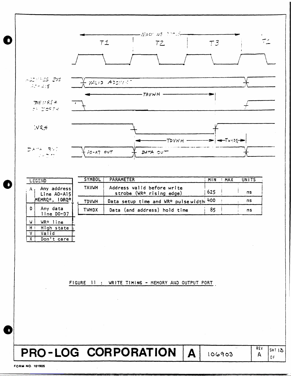
TAVWH I Address
15
..
l
TOVWH
TWHDX
strobe
Data
Data
1
0'---------------------J""·-----
va 1 i d
setup
(and
before
(WR*
r
time
address)
is
and
i ng
hold
wr i te
edge)
WR*
---------------~-I..._jw
.-
..
---
..
---.----
pulsewidth;
time
:f
..
;
MIN
I
I 625
400
i
85
i-;
D
x.~
------\jr------
,
MAX
!
1
!
UNITS
i
I
ns
ns
ns
j
I
i
;
FIGURE
11
•
PRO-LOG
FORM
NO. 101905
CORPORATION
-_=_"A4
:
WR~TE
EAM
I
TIMING -MEMORY
:=
, :
AN~
OUTPUT
A
PORT
#.4WM;_MA##MMU
"";';"'+'
REV
A
SHT
OF
\0

,£1;.
~,#
'.'
/'11
4
T2.
c.,:.J/;'j
/
I
J
I
I
..
T1.
\~_/
A
1"'
:...
'.
. -~ _
~'
•••
,.
::
J>
\
E
-,
- • t:
-!..-
IW
\
/
•
,
~-;1'
J
\
..
~
•
_
...
_-.J\I..-----
;
-1
.1
,~
v
o
LEGEND
A . Any
1
ine
!
~~EMRQ*
'
',,;'AITRQ*
iQ
jc
CLOCK":
Low
iL
!H
High
Val
Iv
address
AO-A1S,
,
10RQ":
state
state
id
-\
I
SYMBOL
TAVQL
TQLCL
TCLQH
NOTE:
PARAMETER
Auo('ess
mus t ee
WAIT
WA
I
TRQ~I:
clock
first
\vAITRQ*
transition
WAIT
MEMRQ~'t
Address
and
Bus
----
val
id
ac
t i ve
state
setup
transition
WAIT
hold
state)
10RQ":
in
state)
time
in
or
.
timing.
j
l....-rc.LoJ-/
before
time
timing
to
insert
this
pr
fn
or
after
T2(for
in
TH.
WA I TRQ-;'t
cycle
to
ior
T2(for
in
TW.
clock
first
is
identical
I
,
i
i
;
!
i
t
I
MIN
185
110
a
to
MAX
,
\
UNITS
I
I
I
I
I
I
ns
ns
ns
/
01
I
t
I
!
i
I
!
I
FIGURE
WAIT
The
or
a
can
REQUEST
WAITRQ*
interrupt
control
also
function
be used
PRO-LOG
FOAM NO. 101905
12:
input
acknow~edge
to
WAITRQ~':
allows
such
single-step
eORPORATION
the
cycle
as
TIMING
7801
to
enter
while
an
analog-to-digital
the
a slow
7801.
(One
WAIT
the
memory
state
WAIT
state
device
converter
A
show!!.l
in any memory, I/O
responds,
finishes.
or
until
WAITRQ*
REV
A
SHT
OF
I
!
I
1°
H

o
I'
) I
,'"
A
'J-i
f;
\ /
=.
.,..",
I
I~
I
T3
B !
L
H
z
V I
Address
Data
I
Contro
!
Low
High
High imp-
edance
I
Va
1 i d
Bus
1
state
state
Bus,
Bus!
\
J
--------------------------~
!
SYMBOL
TQLCH
TCHQH
TKLCH
\
TKLBZ
I
TKHBV
\
PARAMETER
BUSRQ*
BUSRQ*
BUSAK*
I
: Address Bus, Data Bus, and
!
7801
I
I
J
\
T
i
I
I
I
i
:1
~--~~----------~:~
f
~
Ti<LCH~
..
active
(BUSRQ*
active
of
T3
(BUSRQ*
asserted
TH
(Note
most
Control
outputs
is
asserted,
resumes
Address,
Busses
inactive
setup
1)
float
Data,
after
1'1(L.B~.
~
p/::WrN
prior
time)
after
hold
prior
Bus
(Note 2)
after
allowing
drive
6n
and Control
BUSAK*
,
--..------------_
~f
;
·1
(~5
---
i~
\J-~~--------~---.----\(
/'
to
T3
start
time)
to
BUSAK;'~
DMA
operations
the
goes
I
_______
\\-
-a-
MIN
200
o
125
__
._l
f
rJ(~S'/
MAX
;
I
I
;
50
50
UNITS
i ns
;
! ns
L
I
I ns
I
!
I
..--,-
"------
ns
ns
__
...
_-
_
NOTES:
FIGURE
13
: 7801/STO
•
PRO-LOG
FOAM
NO.
101905
CORPORATION
1.
TH
the
DMA
controller
The
2.
BUSAK~\-
MCSYNC1:,
DATA
_"
time
states
7801
has
operations
following
is
active:
STATUS
BUS
00-D7?
BUS
TIMING
••
#:=,;0.;'1#;
are
relinquished
to
proceed
card.
Equivalent
Control
11:,
ADDRESS
FOR
DIRECT
clock
Bus 1 ines
WR*,
STATUS
q 4
periods
the
STO
with
to
R01:,
0":,
BUS
AO-AlS.
MEMORY
A
during
BUS,
an
alternate
808SA
are
floated
10RQ;':,
INTAK:;':,
ACCESS
which
allowing
Hold mode.
when
MEMRQ":,
SYSRESET,':,
(DMA)
4.4
OPERATIONS
:at
4F
i.
Aa;
#4
REv
A
SH T I£)
OF
4#41$
 Loading...