

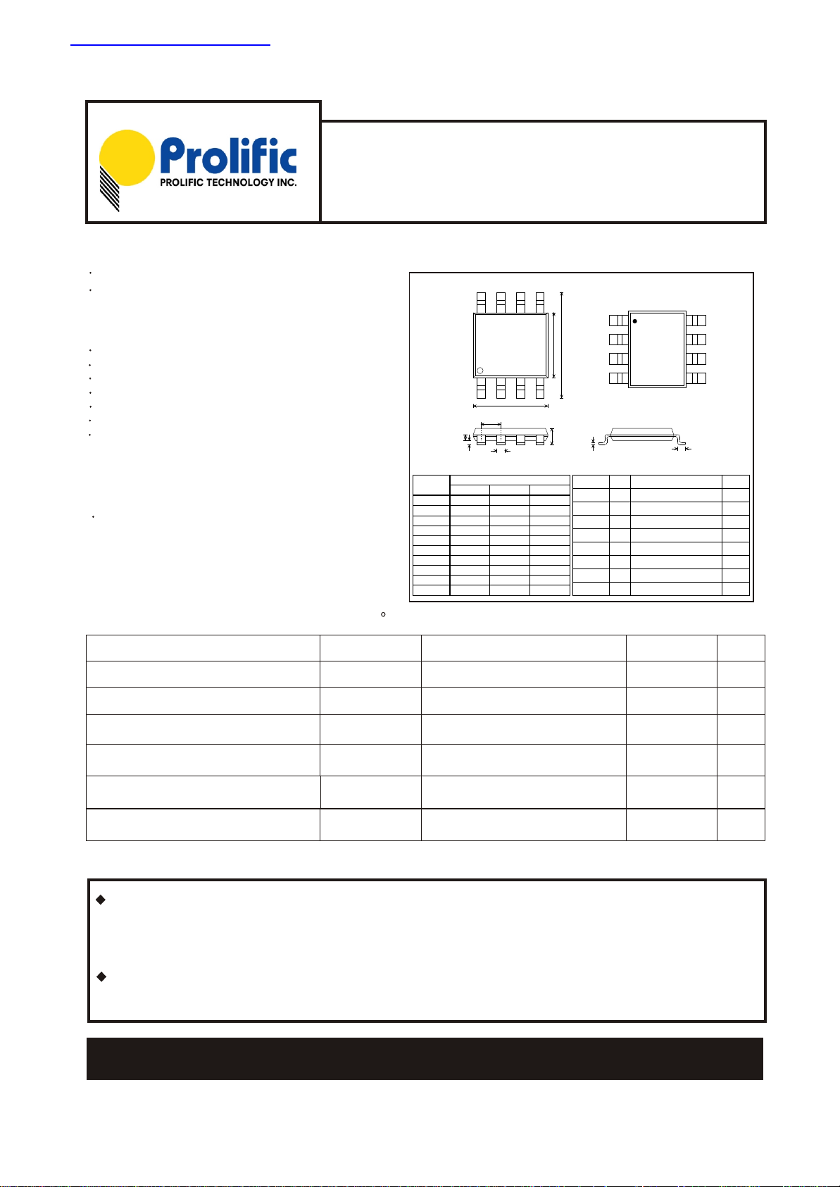
e
LbD
C
H
A2
A1
A
E
SOP 8 L
DIMENSIONS IN MILLIMETERS(mm)
SYMBOLS
MIN NOM MAX
A 1.47 1.60 1.73
A1 0.10 - 0.30
A2 - 1.45 -
B 0.33 0.41 0.51
C 0.19 0.20 0.25
D 4.80 4.85 4.95
E 3.81 3.91 3.99
H 5.79 5.99 6.20
E - 1.27 -
L 0.38 0.71 1.27
O2 3
H+
2 VDD GND
FG
O1
H-
1
PT30DFT
***
RD 4
6
7
8
5
Pin Description
Name Pin Description Type
O1 1 First output pi n O
GND 2 DC ground P
O2 3 Second output pin O
RD 4 Rotation Detecto r(Alarm) O
FG 5 Frequency Generation O
H- 6 Hall element input( -) I
VDD 7 DC power supply P
H+ 8 Hall element input( +) I
查询PT-30DFT(SOP)供应商
DC Brushless Motor Driver IC
PT-30DFT
H - Bridge Driver
Applications
Single coils DC brushless motor.
DC 3.0V~18V.
Features
Single-phase full-wave driver
Motor lock protection and automatic restart
Connectable direct to Hall element
Built-in hysteresis comparator
Frequency Generation output
Rotate Detection (Alarm) output
Low power consumption and high driving efficiency
Input devices
Hall IC
Specifications
Absolute Maximum Ratings (Ta = 25 C)
Parameter
Maximum supply voltage
Allowable power dissipation
Operating temperature
Storage temperature
Symbol
max
VDD
Pd
Ta
Ts
Package: SOP8
Conditions
Ratings
18 V
650
-30 ~ +100
-55 ~ +150
*
Units
m
W
O
C
O
C
Output current
On 50mm x 50mm x 1.6mm glass epoxy board
*
Any and all PROLIFIC products described or contained herein do not have specifications that can handle applications
that require extremely high levels of reliability, such as life-support systems, aircraft's control systems, or other
applications whose failure can be reasonably expected to result in serious physical and/or material damage. Consult
with your PROLIFIC representative nearest you before using any PROLIFIC products described or contained herein in
such applications.
PROLIFIC assumes no responsibility for equipment failures that result from using products at values that exceed, even
momentarily, rated values (such as maximum ratings, operating condition ranges, or other parameters) listed in
products specifications of any and all PROLIFIC products described or contained herein.
Ver 1.5
I0ut
Continoue
Peak
PROLIFIC TECHNOLOGY INC.
7F, No.48, Sec.3, Nan Kang Rd., Nan Kang, Taipei, 115, Taiwan
-1-
400
600
m
m
A
A
Date:Jan. 2002
Electrical Characteristics
Characteristic Symbol Test Condition Min. Typ. Max. Units
Supply Voltage VDD 3 18 V
Output low-level
Voltage
VOL IO=200mA 0.4 0.5 V
Output High-level
Voltage
VOH IO=200mA Vcc-0.5 Vcc-0.4 V
Output Breakdown
Voltage
VBV 18 22 30 V
Input offset
voltage
VOS -6 0 6 mV
Supply Current IDD Output open 3 10 mA
FG/RD flow-in
Current
IFG/IRD Pull-high resistor is
470ohm@12V
25 mA
FG/RD Supply
Voltage
12 30 V
FG Frequency
Same with Hall
input signal
Truth Table
H+ H- State O1 O2 FG RD
H L Rotate H L H L
L H Rotate L H L L
H L Lock L L H H
L H Lock L L H H
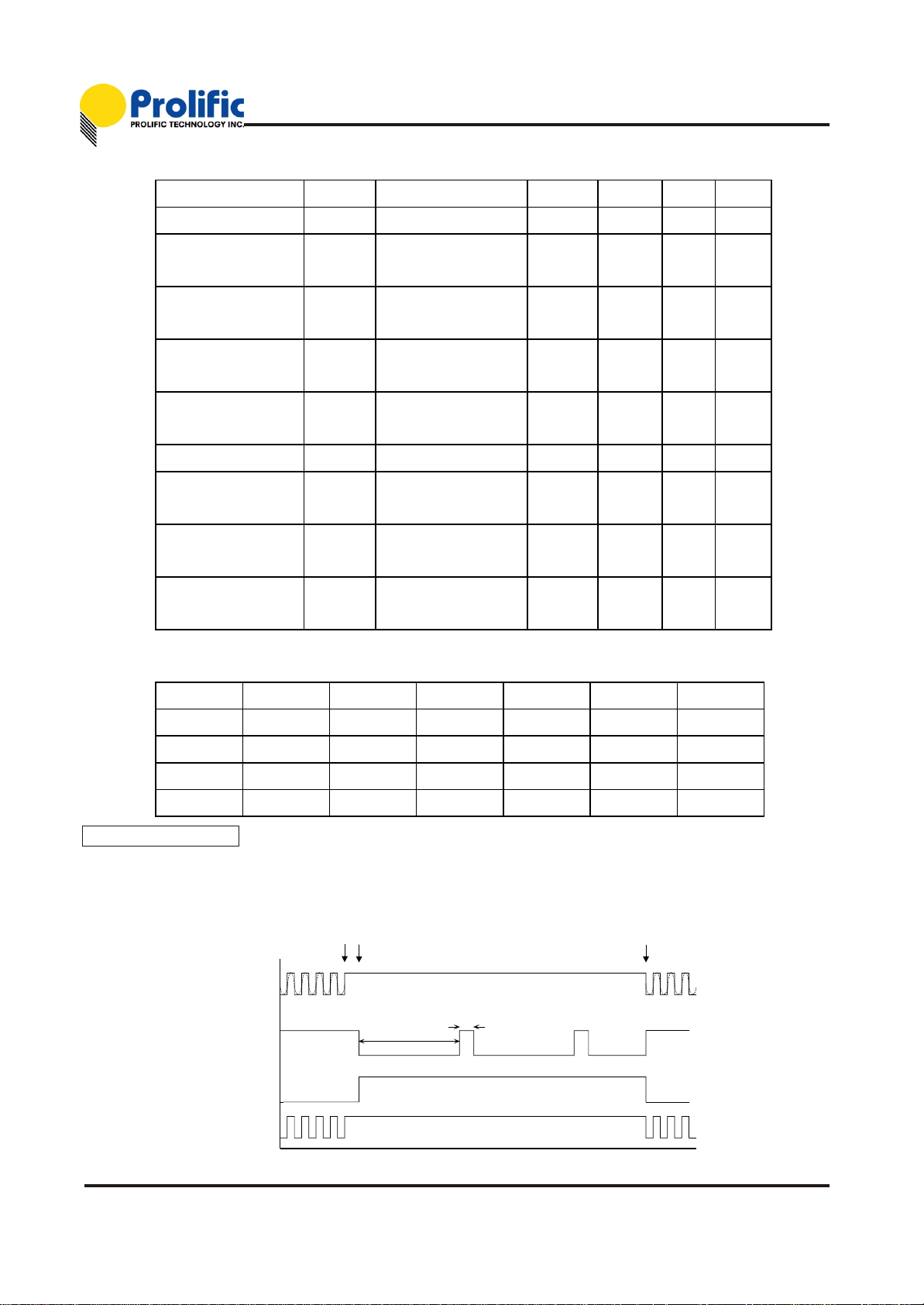
H-/H+
0.3sec
2.1sec
Off
Driver
On
Fig 1. Lock Protection
t
Lock detected
driving
shutdown
rotate
RD
FG
0.3sec
lock
PT-30DFT
Lock Protection
In order to protect the motor, the driver IC will be shutdown to drive the coil when the motor is
locked over 0.3 seconds. Then, it restarts to drive the motor after 2.1 seconds. Figure 1 shows the
timing diagram between the hall input signal and driver's output state.
Ver 1.5
-2-
Date:Jan. 2002

Rotation Frequency and Detector
This driver IC outputs the FG and RD signal for some special application.
For FG application, the driver IC will generate square wave to indicate the motor
rotation frequency. For RD application, the driver IC will output a high signal to
indicate the stop of the motor and a low signal to indicate the normal operation of
the motor. (See Fig. 1)
Pre-Amplifier
This driver IC integrates signal amplifier and the hysteresis comparator in
this chip. The hysteresis comparator uses the hysteresis characteristic to
eliminate noisy oscillations at output of the comparator.
The driver IC architecture block diagram is shown in Fig. 2.
OSC
FG
Lock Timing
Control
Fan Lock
Detection
H-Bridge
Driver
Driver Timing
Control
Vcc
Gnd
O2
O1
FG
Fig. 2. Driver IC Architecture
CMP
OP
Regulator
H-
H+
(Alarm)
RD
RD
PT-30DFT
Ver 1.5
-3-
Date:Jan. 2002

Vcc
Gnd
FG
O2
O1
RD
R0, R1, R4: 10K
R2, R3: open drain loadi ng
Z0: Zener diode, i f VCC=12V,
Vz=12V~18V.The zener diode is optional.
R2
H+
H-
Hall
IC
R0
R1
8
6
5
2
1
3
4
7
R3
VCC
GND
loading
D0
Z0
R4
com
Vcc
Gnd
FG
O2
O1
RD
R0, R1, R4: 10K
R2, R3: open drain l oading
Z0: depend on VCC, if VCC=12V,
Vz=12V~18V.The zener diode i s optional .
R2
H+
H-
Hall
IC
R0
R1
8
6
5
2
1
3
4
7
R3
VCC
GND
loading
D0
Z0
R4
PT-30DFT
Application circuits/
Hall IC input
Hall IC input
*
Single coil
Single coil
Hall IC input
Hall IC input
*
Double coil
Ver 1.5
Note:
R0, R1, R4 is 10K ohm
D0 is general diode, 1/2W
Z0 is 12V~18V zener diode, 1/2W
Com point is floating for double coil
-4-
Date:Jan. 2002

Vcc
Gnd
FG
O2
O1
RD
H-
H+
Hall
IC
R0
R1
6
8
5
2
1
3
4
7
VCC 12V/24V/48V
GND
D0
Z0
R4
R5
R6
R7
R0, R1, R4: 10K
R2, R3: open drain loading
R5: 560,1/2W(for24V); 1.8K,1W(for48V); none( for 12V)
Z0: Zener diode, Vz=12V~18V.
Capcitor is optional for back
e.m.f. protection.
C1 C2
option
Note:
D0: general diode 1/2W, (opti onal)
Z0: Vz=12V zener diode 1/2W
R5: 560,1/2W(for 24V) ; 1. 8K,1W(for 48V); none(for 12V )
R0,R1,R4 : 10K
R6,R7 : 2K, 1/8W(for 0.4A output); 1K, 1/8W(f or 0.8A output), 560, 1/4W (for 1.5A output)
Q1, Q2: depend on driving capability requirement
Ex. 2222A(40V, 0.6A, 0.3W ), 2SD1782/SSTA06(80V, 0.5A, 0.3W ), 2SD1768S(80V, 1A, 0.5W), 2SC4132(120V, 2A 0.5W),
2SD1760(50V, 3A 1W)… ..
C1,C2 : 2.2uF, 50V(optional), or s uitable Vz Zener diode
PT-30DFT
12V(high driving capability)/24V/48V Application circuits
Specifications of any and all PROLIFIC products described or contained herein stipulate the performance,
characteristics, and functions of the described products in the independent state, and are not guarantees of the
performance, characteristics, and functions of the described products as mounted in the customer's products or
equipment. To verify symptoms and states that cannot be evaluated in an independent device, the customer should
always evaluate and test devices mounted in the customer's products or equipment.
PROLIFIC Technology Inc. strives to supply high-quality high-reliability products. However, any and all
semiconductor products fail with some probability. It is possible that these probabilistic failures could give rise to
accidents or events that could endanger human lives, that could give rise to smoke or fire, or that could cause
damage to other property. When designing equipment, adopt safety measures so that these kinds of accidents or
events cannot occur. Such measures include but are not limited to protective
circuits and error prevention circuits for safe design, redundant design, and structural design.
In the event that any and all PROLIFIC products described or contained herein fall under strategic products (including
services) controlled under the Foreign Exchange and Foreign Trade Control Law of Taiwan, such products must not
be exported with our obtaining export license from the Ministry of international Trade and Industry in accordance with
the above law.
No part of this publication may be reproduced or transmitted in any form or by any means, electronic or mechanical,
including photocopying and recording, or any information storage or retrieval system, or otherwise, without the prior
written permission of PROLIFIC Technology Inc.
Any and all information described or contained herein are subject to change without notice due to product/technology
improvement, etc. When designing equipment, refer to theDelivery Specification for the PROLIFIC product that you
intend to use.
Information (including circuit diagrams and circuit parameters) herein is for example only; it is not guaranteed for
volume production. PROLIFIC believes information herein is accurate and reliable, but no guarantees are made or
implied regarding its use or any infringements of intellectual property rights or other rights of third parties.
Specifications and information herein are subject to change without notice.
Ver 1.5
-5-
Date:Jan. 2002
 Loading...