

Page 1
Part Number
Description
SFP-10G-SR-C
10GBASR-SR/SW SFP+ 850nm LC Connectors 300m on MMF, with DOM
function.
Parameter
Symbol
Min
Typ
Max
Unit
Remarks
Data Rate
DR
10.3125
GBd
IEEE 802.3ae
Bit Error Rate
BER
10
12
Operating Temperature
T
OP
0 70
℃
Case temperature
Storage Temperature
T
STO
40
85
℃
Ambient temperature
Supply Current
I
S
180
220
mA
For electrical power
interface
Input Voltage
V
CC
3
3.3
3.6
V
Maximum Voltage
V
MAX
0.5
4 V
For electrical power
interface
PROLABS – SFP-10G-SR-C
10GBd SFP+ Short Wavelength (850nm) Transceiver
SFP-10G-SR-C Overview
PROLABS’s SFP-10G-SR-C SFP optical transceivers are based on 10G
Ethernet IEEE 802.3ae standard and SFF 8431 standard, and provide a
quick and reliable interface for the 10G Ethernet application. The Digital
diagnostics functions are available via 2-wire serial bus specified in the
SFF 8472.
Product Features
Up to 10.5 GBd bi-directional data links
Compliant with IEEE 802.3ae 10GBASE-SR/SW
Compliant with SFF8431
Hot-pluggable SFP+ footprint
850nm VCSEL laser transmitter
Duplex LC connector
Built-in digital diagnostic functions
Up to 300m on OM3 MMF
Single power supply 3.3V
RoHS Compliance
Class 1 laser product complies with EN 60825-1
Operating temperature range: 0℃ to 70℃.
Applications
10GBASE-SR/SW Ethernet
Ordering Information
General Specifications
Page 2
Parameter
Fiber Type
Modal Bandwidth @
850nm (MHz-km)
Distance Range (m)
9.95 – 10.5 GBd
62.5/125um MMF
160
2-26
62.5/125um MMF
200
2-33
50/125um MMF
400
2-66
50/125um MMF
500
2-82
50/125um MMF
2000
2-300
Parameter
Symbol
Min
Typ
Max
Unit
Remarks
Output Optical Power
P
TX
5 1
dBm
Class 1 Product
Optical Center Wavelength
C
840 860
nm
Optical Modulation Amplitude
OMA
1.5dB
IEEE 802.3ae
Extinction Ratio
ER
3
5.5 dB
Spectral Width (RMS)
0.45
nm
Relative Intensity Noise
RIN
128
dB/Hz
Transmitter Dispersion Penalty
TDP
3.9
dB
Transmitter Jitter
According to IEEE 802.3ae requirement
Launch Power of OFF
Transmitter
P
OUT_OFF
– 30
dBm
Average
Parameter
Symbol
Min
Typ
Max
Unit
Remarks
Optical Center Wavelength
C
840 860
nm
Receiver Sensitivity (OMA)@
10.3GBd
R
X_SEN1
11.1
dBm
Measured with worst
ER:
BER<10
-12 231
-1 PRBS
Stressed Receiver Sensitivity in OMA
@ 10.3Gb/s
P
SENS2
– 7.5
dBm
IEEE 802.3ae
Maximum Input Power
P
IN
0.5
dBm
Receiver Reflectance
TRRX
– 12
dB
LOS Assert
LOSA
– 30
dBm
LOS De-Assert
LOS
D
– 12
dBm
LOS Hysteresis
0.5
dB
Link Distances
Optical Characteristics – Transmitter
VCC=3V to 3.6V, TC=0℃ to 70℃
Optical Characteristics – Receiver
VCC=3V to 3.6V, TC=0℃ to 70℃
Page 3
Parameter
Symbol
Min
Typ
Max
Unit
Remarks
Input differential impedance
R
IN
100 Ω
Non condensing
Single ended data input swing
V
IN_PP
250 800
mV
Transmit disable voltage
V
D
2 V
CC
V
Transmit enable voltage
V
EN
V
EE
VEE+0.8 V
Parameter
Symbol
Min
Typ
Max
Unit
Remarks
Single ended data output swing
V
OUT_PP
150
300
425
mV Data output rise time (20%-80%)
T
R
30 ps
Data output fall time (20%-80%)
T
F
30 ps
LOS Fault
V
LOS_Fault
2 V
CC_HO
ST
V
LOS Normal
V
LOS_normal
V
EE
VEE+0.5 V
Parameter
Symbol
Accuracy
Units
Report Range
Unit
Remarks
Internal Calibration
Temperature
T
MON
±3
℃
5
75
℃
Voltage
V
MON
±0.1
V
2.9
3.7
V
Bias Current
I
MON
±10
%
1
15
mA
Tx Power
P
MON
±3
dB
10
0 dBm
Rx Power
P
MON
±3
dB
20
0
dBm
Electrical Characteristics – Transmitter
VCC=3V to 3.6V, TC=0℃ to 70℃
Electrical Characteristics – Receiver
VCC=3V to 3.6V, TC=0℃ to 70℃
Digital Diagnostic Functions
SFP-10G-SR-C support the 2-wire serial communication protocol as defined in the SFF 8472. Digital
diagnostic information are accessible over the 2-wire interface at the address 0xA2. Digital
Diagnostics for SFP-10G-SR-C are internally calibrated by default. A micro controller unit inside the
transceiver gathers the monitoring information and reports the status of transceiver.
Transceiver Temperature, internally measured, represented as a 16 bit signed twos complement
value in increments of 1/256 degrees Celsius, Temperature accuracy is better than ±3 degrees
Celsius over specified operating temperature and voltage.
Transceiver Supply Power, internally measured, represented as a 16 bit unsigned integer with the
voltage defined as the full 16 bit value (0 – 65535) with LSB equal to 100 µVolt, yielding a total range
of 0 to +6.55 Volts.
Transceiver TX bias current, internally measured, represented as a 16 bit unsigned integer with the
current defined as the full 16 bit value (0 – 65535) with LSB equal to 2 µA, yielding a total range of 0
to 131mA. Accuracy is better than ±10% over specified operating temperature and voltage.
Transceiver TX output power, internally measured, represented as a 16 bit unsigned integer with
the power defined as the full 16 bit value (0 – 65535) with LSB equal to 0.1 µW. Data is assumed to
be based on measurement of laser monitor photodiode current. Accuracy is better than ±3dB over
specified temperature and voltage. Data is not valid when the transmitter is disabled.
Transceiver RX received optical power, internally measured, represented as a 16 bit unsigned
integer with the power defined as the full 16 bit 35 value (0 – 65535) with LSB equal to 0.1 µW.
Accuracy is better than ±3dB over specified temperature and voltage.
Page 4
ELECTRICAL
SUBASSEMBLY
Micro
TX_FAULT
TX_DATA
TX_DATA\
TX_DISABLE
RX_DATA
RX_DATA\
RX_LOS
SDA
SCL
MOD_ABS
OPTICAL
SUBASSEMBLY
OPTICAL SUBASSEMBLY
PRE AMP
DUPLEX LC
RECEPTACLE
Safety Control
LD Driver
Limiting Amp
LOS Detect
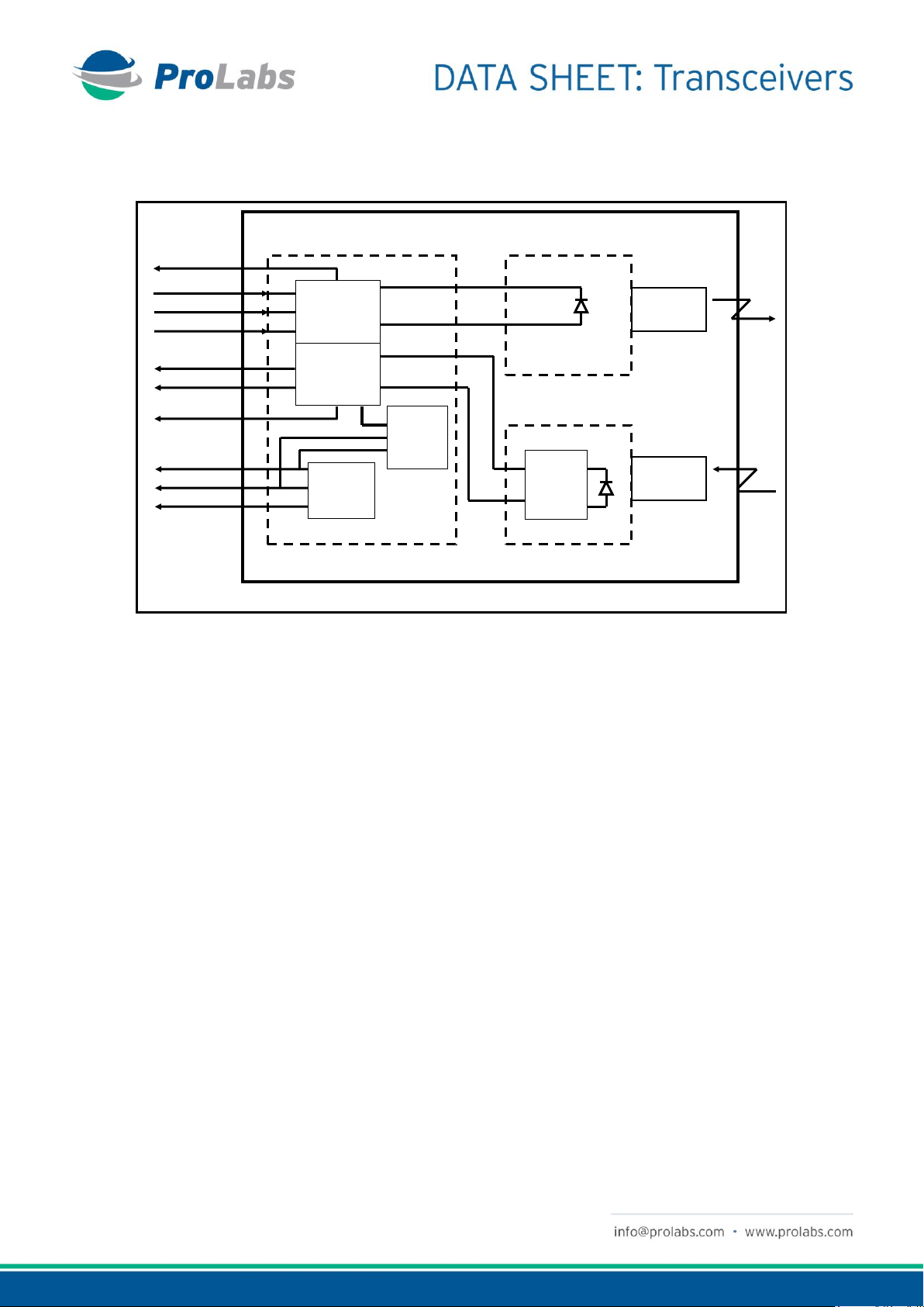
Block Diagram of Transceiver
Transmitter Section
The VCSEL driver accept differential input data and provide bias and modulation currents for driving a
laser. An automatic power-control (APC) feedback loop is incorporated to maintain a constant
average optical power. 850 nm VCSEL in an eye safe optical subassembly (OSA) mates to the fiber
cable.
TX_DISABLE
The TX_DISABLE signal is high (TTL logic “1”) to turn off the laser output. The laser will turn on within
1ms when TX_DISABLE is low (TTL logic “0”).
TX_FAULT
When the TX_FAULT signal is high, output indicates a laser fault of some kind. Low indicates normal
operation.
Receiver Section
The receiver utilizes a PIN detector integrated with a trans-impedance preamplifier in an OSA. This
OSA is connected to a Limiting Amplifier which providing post-amplification quantization, and optical
signal detection. The limiting Amplifier is AC-coupled to the transimpedance amplifier, with internal
100Ω differential termination.
Receive Loss (RX_LOS)
The RX_LOS is high (logic “1”) when there is no incoming light from the companion transceiver. This
signal is normally used by the system for the diagnostic purpose. The signal is operated in TTL level.
Controller Section
The micro controller unit monitors the operation information of LD driver and Limiting Amplifier. And
report these status to the customer.
Page 5
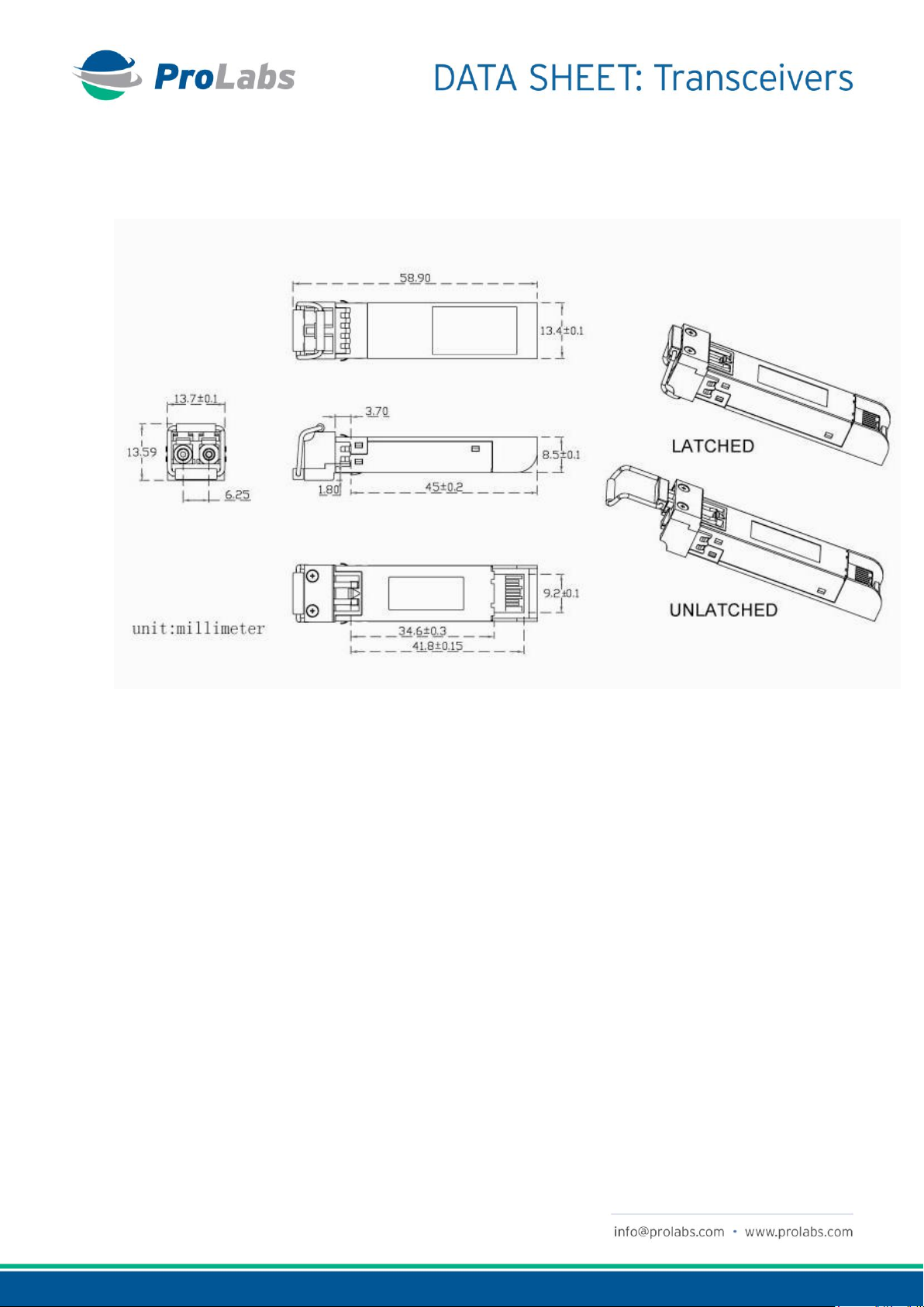
Dimensions
ALL DIMENSIONS ARE ±0.2mm UNLESS OTHERWISE SPECIFIED
UNIT: mm
Page 6
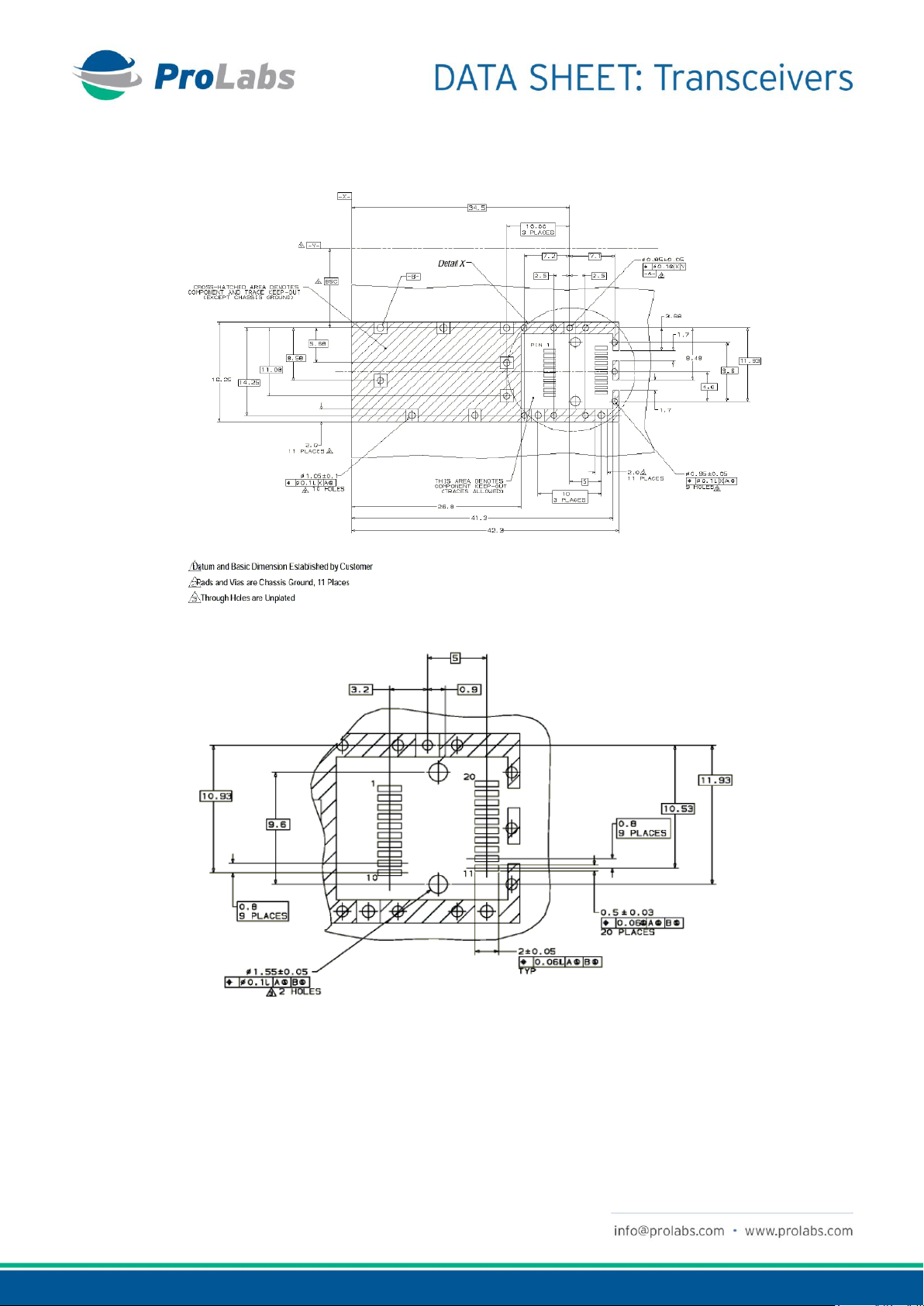
PCB Layout Recommendation
Page 7
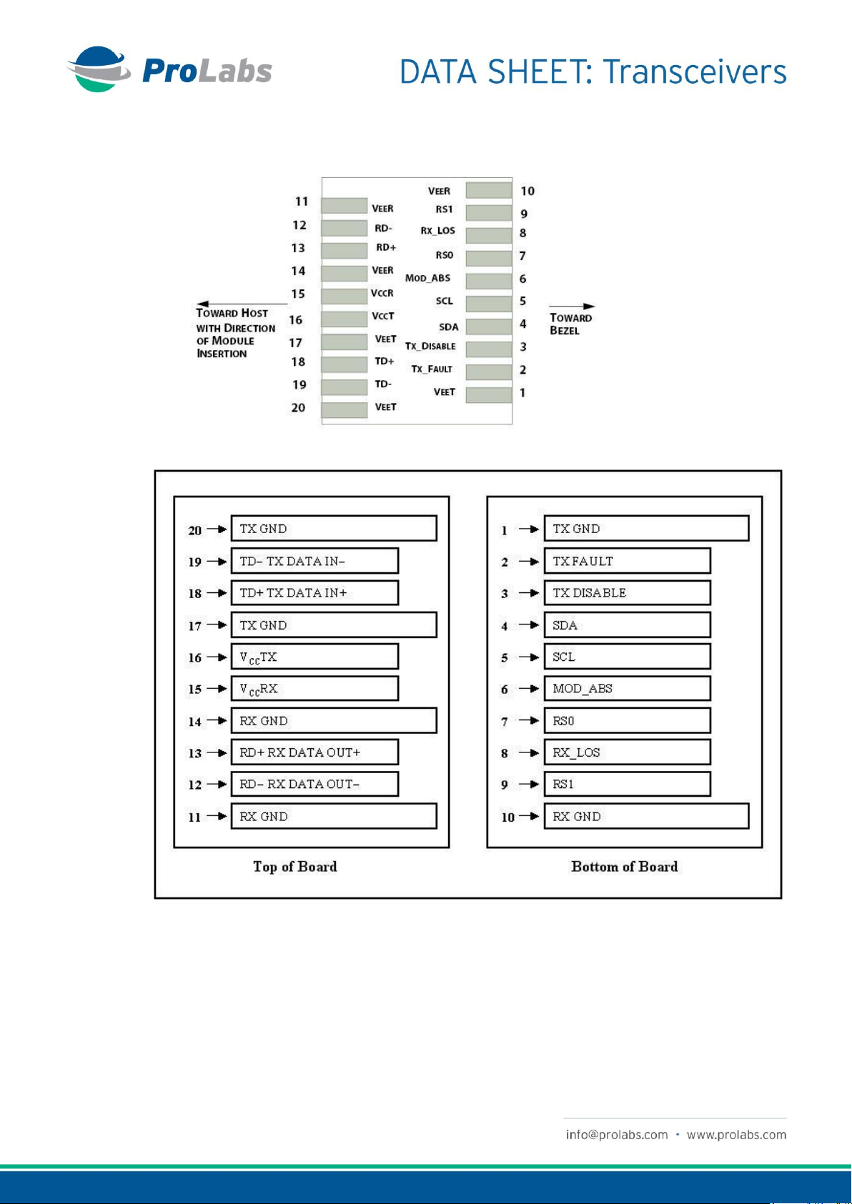
Electrical Pad Layout
Page 8
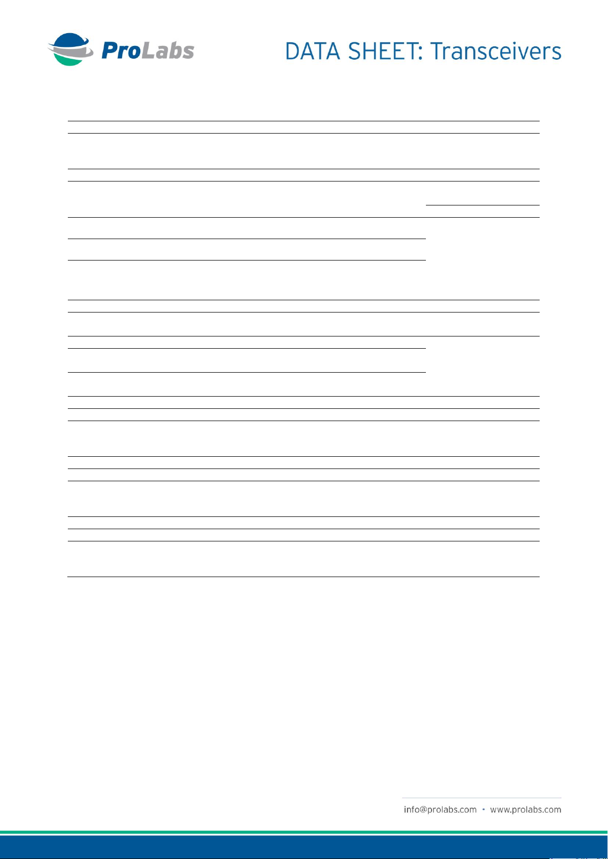
PIN #
Symbol
Description
Remarks
1
V
EET
Transmitter ground (common with receiver
ground)
Circuit ground is
isolated
from chassis ground
2
T
FAULT
Transmitter Fault.
3
T
DIS
Transmitter Disable. Laser output disable on high
or open
Disabled: T
DIS
>2V or
open
Enabled: T
DIS
<0.8V
4
SDA
Data line for serial ID
Should Be pulled up
with
4.7k – 10k ohm on
host
board to a voltage
between
2V and 3.6V
5
SCL
Clock line for serial ID
6
MOD_ABS
Module Absent. Grounded within the module
7
RS0
No connection required
8
LOS
Loss of Signal indication. Logic 0 indicates normal
operation
LOS is open collector
output 9 RS1
No connection required
Circuit ground is
isolated
from chassis ground
10
V
EER
Receiver ground (common with transmitter
ground)
11
V
EER
Receiver ground (common with transmitter
ground)
12
RD–
Receiver Inverted DATA out. AC coupled
13
RD+
Receiver Non-inverted DATA out. AC coupled
14
V
EER
Receiver ground (common with transmitter
ground)
Circuit ground is
isolated
from chassis ground
15
V
CCR
Receiver power supply
16
V
CCT
Transmitter power supply
17
V
EET
Transmitter ground (common with receiver
ground)
Circuit ground is
connected to chassis
ground
18
TD+
Transmitter Non-Inverted DATA in. AC coupled
19
TD–
Transmitter Inverted DATA in. AC coupled
20
V
EET
Transmitter ground (common with receiver
ground)
Circuit ground is
connected to chassis
ground
Pin Assignment
References
1. IEEE standard 802.3ae. IEEE Standard Department, 2005.
2. Enhanced 8.5 and 10 Gigabit Small Form Factor Pluggable Module “SFP+” – SFF-8431
3. Digital Diagnostics Monitoring Interface for Optical Transceivers – SFF-8472.
 Loading...