

Page 1

VPC3+C
User Manual
Revision 1.03
The C lever Alternative
Page 2

Liability Exclusion
We have tested the contents of this document regarding
agreement with the hardware and software described.
Nevertheless, there may be deviations and we do not
guarantee complete agreement. The data in the
document is tested periodically, however. Required
corrections are included in subsequent versions. We
gratefully accept suggestions for improvements.
Copyright
Copyright © profichip GmbH 2004-2006.
All Rights Reserved.
Unless permission has been expressly granted, passing
on this document or copying it, or using and sharing its
content are not allowed. Offenders will be held liable. All
rights reserved, in the event a patent is granted or a
utility model or design is registered.
This document is subject to technical changes.
2 Revision 1.03
VPC3+C
User Manual
Copyright © profichip GmbH 2004-2006
Page 3

Table of Contents
1 Introduction.................................................................5
2 Functional Description...............................................7
2.1 Overview ......................................................................................7
3 Pin Description............................................................9
3.1 Pin Assignment ............................................................................9
3.2 Pinout .........................................................................................11
4 Memory Organization ...............................................13
4.1 Overview ....................................................................................13
4.2 Control Parameters (Latches/Registers)....................................15
4.3 Organizational Parameters (RAM) .............................................17
5 ASIC Interface............................................................19
5.1 Mode Registers ..........................................................................19
5.1.1 Mode Register 0 .............................................................19
5.1.2 Mode Register 1 .............................................................21
5.1.3 Mode Register 2 .............................................................23
5.2 Status Register...........................................................................25
5.3 Interrupt Controller .....................................................................27
5.3.1 Interrupt Request Register.............................................. 28
5.3.2 Interrupt Acknowledge / Mask Register .......................... 31
5.4 Watchdog Timer.........................................................................31
5.4.1 Automatic Baud Rate Identification................................. 32
5.4.2 Baud Rate Monitoring ..................................................... 32
5.4.3 Response Time Monitoring.............................................32
6 PROFIBUS DP Interface............................................35
6.1 DP Buffer Structure ....................................................................35
6.2 Description of the DP Services...................................................38
6.2.1 Set_Slave_Add (SAP 55) ...............................................38
6.2.2 Set _Prm (SAP 61) .........................................................39
6.2.3 Chk_Cfg (SAP 62) ..........................................................43
6.2.4 Slave_Diag (SAP 60)......................................................44
6.2.5 Write_Read_Data / Data_Exchange (Default_SAP)....... 46
6.2.6 Global_Control (SAP 58) ................................................50
6.2.7 RD_Input (SAP 56) ......................................................... 51
6.2.8 RD_Output (SAP 57) ......................................................51
6.2.9 Get_Cfg (SAP 59)...........................................................52
VPC3+C User Manual
Revision 1.03 3
Copyright © profichip GmbH 2004-2006
Page 4

Table of Contents
7 PROFIBUS DP Extensions .......................................53
7.1 Set_(Ext_)Prm (SAP 53 / SAP 61).............................................53
7.2 PROFIBUS DP-V1 .....................................................................54
7.2.1 Acyclic Communication Relationships ............................ 54
7.2.2 Diagnosis Model .............................................................57
7.3 PROFIBUS DP-V2 .....................................................................58
7.3.1 DXB (Data eXchange Broadcast) ................................... 58
7.3.2 IsoM (Isochron Mode).....................................................64
8 Hardware Interface....................................................69
8.1 Universal Processor Bus Interface.............................................69
8.1.1 Overview.........................................................................69
8.1.2 Bus Interface Unit ...........................................................69
8.1.3 Application Examples (Principles) ..................................73
8.1.4 Application with 80C32 (2K Byte RAM Mode) ................75
8.1.5 Application with 80C32 (4K Byte RAM Mode) ................76
8.1.6 Application with 80C165 .................................................77
8.2 Dual Port RAM Controller...........................................................77
8.3 UART..........................................................................................78
8.4 ASIC Test...................................................................................78
9 PROFIBUS Interface..................................................79
9.1 Pin Assignment ..........................................................................79
9.2 Example for the RS485 Interface ...............................................80
10 Operational Specifications.......................................81
10.1 Absolute Maximum Ratings........................................................81
10.2 Recommended Operating Conditions ........................................81
10.3 General DC Characteristics........................................................81
10.4 Ratings for the Output Drivers ....................................................82
10.5 DC Electrical Characteristics Specification for 5V Operation .....82
10.6 DC Electrical Characteristics Specification for 3.3V Operation ..83
10.7 Timing Characteristics ................................................................84
10.7.1 System Bus Interface......................................................84
10.7.2 Timing in the Synchronous Intel Mode ...........................85
10.7.3 Timing in the Asynchronous Intel Mode..........................87
10.7.4 Timing in the Synchronous Motorola Mode .................... 89
10.7.5 Timing in the Asynchronous Motorola Mode ..................91
10.8 Package .....................................................................................94
10.9 Processing Instructions ..............................................................96
4 Revision 1.03
VPC3+C
User Manual
Copyright © profichip GmbH 2004-2006
Page 5

Introduction 1
1 Introduction
Profichip’s VPC3+C is a communication chip with processor interface for
intelligent PROFIBUS DP-Slave applications. It’s an enhancement of the
VPC3+B in terms of protocol functions and power consumption.
The VPC3+C handles the message and address identification, the data
security sequences and the protocol processing for PROFIBUS DP. In
addition the acyclic communication and alarm messages, described in
DPV1 extension, are supported. Furthermore the slave-to-slave
communication Data eXchange Broadcast (DXB) and the Isochronous Bus
Mode (IsoM), described in DPV2 extension, are also provided.
Automatic recognition and support of data transmissions rates up to 12
Mbit/s, the integration of the complete PROFIBUS DP protocol, 4K Byte
communication RAM and the configurable processor interface are features
to create high-performance PROFIBUS DP-Slave applications. The device
can be operated with either 3.3V or 5V single supply voltage. For 3.3V
operation the inputs are 5V tolerant.
Profichip’s VPC3+ is the predecessor of VPC3+C and VPC3+B. The chip
offers 2 kByte communication RAM and PROFIBUS DP functionality only
and is therefore suited for DP-Slave applications which do not require
DP-V1 or DP-V2 functions. The device can be operated with 5V single
supply only.
VPC3+ and VPC3+C are pin-compatible. Therefore VPC3+ can be
replaced by VPC3+C in existing applications without any restrictions or SWmodifications. However, downgrading from VPC3+C to VPC3+ is only
possible, if the additional features of VPC3+C (4K Byte RAM, DP-V1- or
DP-V2-functionality, 3.3V supply) are not used.
As there are also simple devices in the automation engineering area, such
as switches or thermoelements, that do not require a microcontroller for
data preprocessing, profichip offers a DP-Slave ASIC with 32 direct
input/output bits. The VPCLS2 handles the entire data traffic independently.
No additional microprocessor or firmware is necessary. The VPCLS2 is
compatible to existing chips.
Further information about our products or current and future projects is
available on our web page:
http://www.profichip.com.
VPC3+C User Manual
Revision 1.03 5
Copyright © profichip GmbH 2004-2006
Page 6

1 Introduction
Notes:
6 Revision 1.03
VPC3+C
User Manual
Copyright © profichip GmbH 2004-2006
Page 7

Functional Description 2
2 Functional Description
2.1 Overview
The VPC3+C makes a cost optimized design of intelligent PROFIBUS DPSlave applications possible.
The processor interface supports the following processor series:
Intel: 80C31, 80X86
Siemens: 80C166/165/167
Motorola: HC11-, HC16-, and HC916 types
The VPC3+C handles the physical layer 1 and the data link layer 2 of the
ISO/OSI-reference-model excluding the analog RS485 drivers.
The integrated 4K Byte Dual-Port-RAM serves as an interface between
the VPC3+C and the software/application. In case of using 2K Byte the
entire memory is divided into 256 segments, with 8 bytes each. Otherwise
in the 4K Byte mode the segment base addresses starts at multiple of 16.
Addressing by the user is done directly, however, the internal Micro
Sequencer (MS) addresses the RAM by means of the so-called basepointer. The base-pointer can be positioned at the beginning of a segment
in the memory. Therefore, all buffers must be located at the beginning of a
segment.
If the VPC3+C carries out a DP communication it automatically sets up all
DP-SAPs. The various telegram information are made available to the user
in separate data buffers (for example, parameter and configuration data).
Three buffers are provided for data communication (three for output data
and three for input data). As one buffer is always available for communication no resource problems can occur. For optimal diagnosis support, the
VPC3+C offers two Diagnosis-Buffers. The user enters the updated
diagnosis data into these buffers. One Diagnosis-Buffer is always assigned
to the VPC3+C.
The Bus Interface Unit is a parameterizable synchronous/asynchronous 8-
bit interface for various Intel and Motorola microcontrollers/processors. The
user can directly access the internal 2K/4K Byte RAM or the parameter
latches and control registers via the 11/12-bit address bus.
Procedure-specific parameters (Station_Address, control bits, etc.) must be
transferred to the Parameter Registers and to the Mode Registers after
power-on.
The MAC status can be observed at any time in the Status Register.
Various events (e.g. various indications, error events, etc.) are entered in
the Interrupt Controller. These events can be individually enabled via a
mask register. Acknowledgement takes place by means of the acknowledge register. The VPC3+C has a common interrupt output.
VPC3+C User Manual
Revision 1.03 7
Copyright © profichip GmbH 2004-2006
Page 8

2 Functional Description
The integrated Watchdog Timer is operated in three different states:
BAUD_SEARCH, BAUD_CONTROL and DP_CONTROL.
The Micro Sequencer (MS) controls the entire process. It contains the DP-
Slave state machine (DP_SM).
The integrated 4K Byte RAM that operates as a Dual-Port-RAM contains
procedure-specific parameters (buffer pointer, buffer lengths,
Station_Address, etc.) and the data buffers.
In the UART, the parallel data flow is converted into the serial data flow and
vice-versa. The VPC3+C is capable of automatically identifying the baud
rates (9.6 Kbit/s - 12 Mbit/s).
The Idle Timer directly controls the bus times on the serial bus line.
8 Revision 1.03
VPC3+C
User Manual
Copyright © profichip GmbH 2004-2006
Page 9
Pin Description 3
3 Pin Description
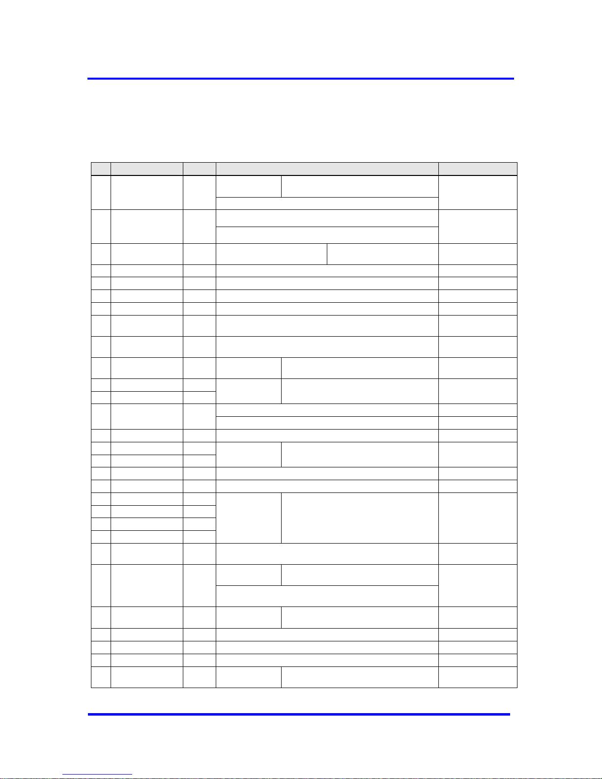
3.1 Pin Assignment
Pin Signal Name In/Out Description Source / Destination
XCS Chip-Select
C32 Mode (2K Byte RAM): connect to VDD
C165 Mode: CS-Signal
1
AB11
I(C)
Address Bus 11 (C32-Mode; 4K Byte RAM)
CPU (80C165)
XWR / E_CLOCK Write Signal / E_Clock for Motorola
2
AB11
I(C)
Address Bus 11 (Asynchronous Motorola Mode; 4K Byte RAM)
CPU
3 DIVIDER I(C)
Setting the scaling
factor for CLKOUT2/4
‘0’ = CLK divided by 4
’1’ = CLK divided by 2
Configuration Pin
4 XRD / R_W I(C) Read Signal / Read _Write for Motorola CPU
5 CLK I(TS) System Clock Input, 48 MHz System
6 VSS
7 CLKOUT2/4 O Clock Output (System Clock divided by 2 or 4) System, CPU
8 XINT/MOT I(C)
‘0’ = Intel Interface
’1’ = Motorola Interface
Configuration Pin
9 X/INT O Interrupt
CPU; InterruptController
10 AB10 I(CPD) Address Bus
C32 Mode: ‘0’
C165 Mode: Address Bus
System, CPU
11 DB0 I(C)/O
12 DB1 I(C)/O
Data Bus
C32 Mode: Data/Address Bus multiplexed
C165 Mode: Data/Address Bus separated
CPU, Memory
XDATAEXCH Indicates DATA-EXCH state for PROFIBUS DP LED
13
SYNC
O
Synchronization Signal for Isochron Mode (see section 8.3.2) CPU
14 XREADY/XDTACK O Ready for external CPU System, CPU
15 DB2 I(C)/O
16 DB3 I(C)/O
Data Bus
C32 mode: Data /Address Bus multiplexed
C165 mode: Data/Address Bus separate
CPU, Memory
17 VSS
18 VDD
19 DB4 I(C)/O
20 DB5 I(C)/O
21 DB6 I(C)/O
22 DB7 I(C)/O
Data Bus
C32 mode: Data/Address Bus multiplexed
C165 mode: Data/Address Bus separate
CPU, Memory
23 MODE I
‘0’ = 80C166 Data/Address Bus separated; Ready Signal
’1’ = 80C32 Data/Address Bus multiplexed, fixed Timing
Configuration Pin
ALE / AS
Address Latch
Enable
C32 mode: ALE
C165 mode: ‘0’ (2K Byte RAM)
24
AB11
I(C)
Address Bus 11 (Asynchronous Intel and
Synchronous Motorola Mode; 4K Byte RAM)
CPU
25 AB9 I Address Bus
C32 Mode: <log>0
C165 Mode: Address Bus
CPU, Memory
26 TXD O Serial Transmit Port PROFIBUS Interface
27 RTS O Request to Send PROFIBUS Interface
28 VSS
29 AB8 I(C) Address Bus
C32 mode: ‘0’
C165 mode: Address Bus
CPU, Memory
VPC3+C User Manual
Revision 1.03 9
Copyright © profichip GmbH 2004-2006
Page 10
3 Pin Description
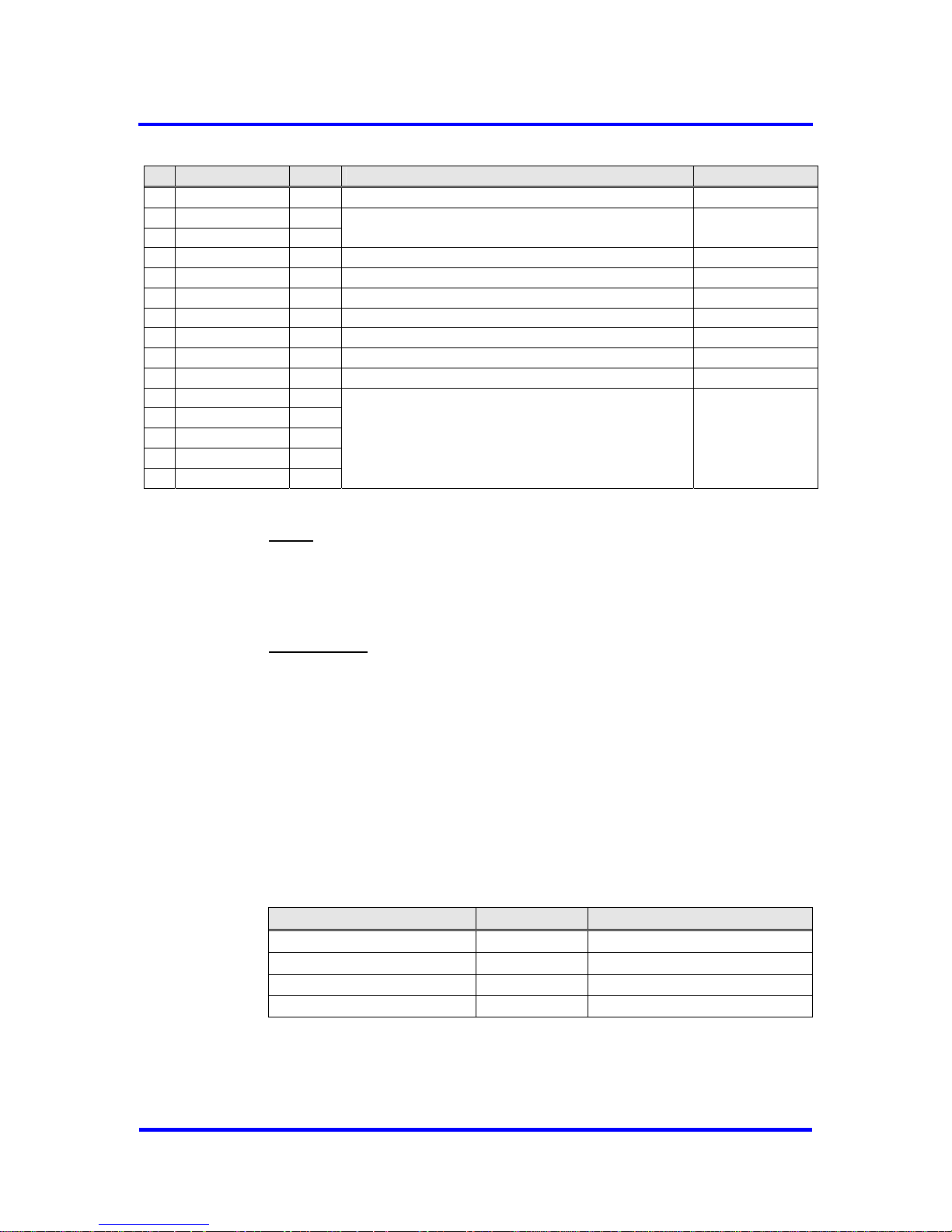
Pin Signal Name In/Out Description Source / Destination
30 RXD I(C) Serial Receive Port PROFIBUS Interface
31 AB7 I(C)
32 AB6 I(C)
Address Bus CPU, Memory
33 XCTS I(C) Clear to Send: ‘0’ = send enable FSK Modem
34 XTEST0 I(C) Pin must be connected to VDD.
35 XTEST1 I(C) Pin must be connected to VDD.
36 RESET I(CS) Connect Reset Input with CPU’s port pin.
37 AB4 I(C) Address Bus CPU, Memory
38 VSS
39 VDD
40 AB3 I(C)
41 AB2 I(C)
42 AB5 I(C)
43 AB1 I(C)
44 AB0 I(C)
Address Bus CPU, Memory
Figure 3-1: Pin Assignment
Notes: All signals that begin with X.. are LOW active.
C32-Mode means ‘Synchronous Intel Mode’ and
C165-Mode means ‘Asynchronous Intel Mode’.
VDD = +5 V
VSS = 0 V
Input Levels:
I ( C ) : CMOS
I ( CS ) : CMOS, Schmitt-Trigger
I (CPD ) : CMOS, pulldown
I (TS ) : TTL, Schmitt-Trigger
4K Byte RAM extension
Beginning with Step B of the VPC3+ the communication RAM has been
extended to 4K Byte, whereas Step A only has 2K Byte. To access the
entire 4K Byte RAM in VPC3+C an additional address signal AB11 is
required. Which pin is assigned to A11 depends on the Processor Interface
Mode used (see Figure 3-2). Due to compatibility reasons the pin which is
now assigned to A11 was unused in Step A for the certain Interface Mode.
Processor Interface Mode Pin Signal Name
Synchronous Intel Mode 1 XCS
Asynchronous Intel Mode 24 ALE/AS
Asynchronous Motorola Mode 2 XWR/E_CLOCK
Synchronous Motorola Mode 24 ALE/AS
Figure 3-2 : Pin assignment for AB11
The 4K Byte RAM extension must be enabled in Mode Register 2 (see
section 5.1.3). By default the 4K Byte mode is disabled.
10 Revision 1.03
VPC3+C
User Manual
Copyright © profichip GmbH 2004-2006
Page 11

Pin Description 3
3.2 Pinout
VPC3+C has a 44-pin PQFP housing with the following pinout:
DB7
DB6
DB5
DB4
VDD
VSS
DB3
DB2
XREADY/XDTACK
XDATAEXCH/SYNC
DB1
XCS/AB11
WR/E_CLOCK/AB11
DIVIDER
XRD/R_W
CLK
VSS
CLCKOUT2/4
XINT/MOT
X/INT
AB10
DB0
XCTS
AB6
AB7
RXD
AB8
VSS
RTS
TXD
AB9
ALE/AS/AB11
MODE
XTEST0
XTEST1
RESET
AB4
VSS
VDD
AB3
AB2
AB5
AB1
AB0
111
12
22
2333
34
44
Figure 3-3: VPC3+C Pinout
For details about package outline and dimensions see section 10.8.
VPC3+C User Manual
Revision 1.03 11
Copyright © profichip GmbH 2004-2006
Page 12

3 Pin Description
Notes:
12 Revision 1.03
VPC3+C
User Manual
Copyright © profichip GmbH 2004-2006
Page 13

Memory Organization 4
4 Memory Organization
4.1 Overview
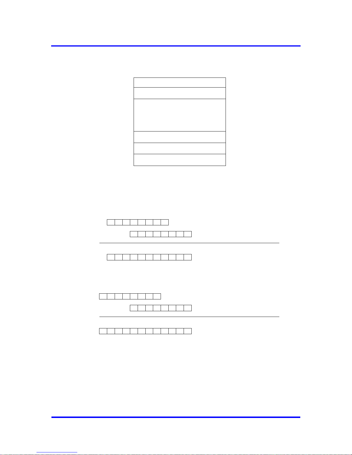
The internal Control Parameters are located in the first 21 addresses. The
latches/registers either come from the internal controller or influence the
controller. Certain cells are read- or write-only. The internal working cells,
which are not accessible by the user, are located in RAM at the same
address locations.
The Organizational Parameters are located in RAM beginning with address
16H. The entire buffer structure (for the DP-SAPs) is based on these parameters. In addition, general parameter data (Station_Address,
Ident_Number, etc.) and status information (Global_Control command, etc.)
are also stored in these cells.
Corresponding to the parameter setting of the Organizational Parameters,
the user-generated buffers are located beginning with address 40H. All
buffers or lists must begin at segment addresses (8 bytes segmentation for
2K Byte mode, 16 bytes segmentation for 4K Byte mode).
Address Function
000H
:
015H
Control Parameters
(latches/registers) (21 bytes)
Internal working cells
016H
:
03FH
Organizational Parameters (42 bytes)
040H
:
7FFH (FFFH)
DP-buffers: Data in (3)*
Data out (3)**
Diagnosis data(2)
Parameter data (1)
Configuration data (2)
Auxiliary buffers (2)
SSA-buffer (1)
DP-V1-buffer: SAP-List (1)
Indication / Response buffers ***
DP-V2-buffer: DXB out (3)****
DXB-buffers (2)
CS-buffers (1)
Figure 4-1: Memory Table
* Data in means input data from DP-Slave to DP-Master
** Data out means output data from DP-Master to DP-Slave
*** number of buffers depends on the entries in the SAP-List
**** DXB out means input data from another DP-Slave (slave-to-slave communication)
VPC3+C User Manual
Revision 1.03 13
Copyright © profichip GmbH 2004-2006
Page 14
4 Memory Organization
Internal VPC3+C RAM (2K/4K Byte)
Segment 0
Segment 1
Segment 2
8/16 bit segment addresses
(pointer to the buffers)
Segment 254
Segment 255
Building of the physical buffer address:
2K Byte Mode:
7 0
Segment base address (8 bit)
0 0 0 0 0 Offset (3 bit)
+
10 0
Physical address (11 bit)
4K Byte Mode:
7 0
Segment base address (8 bit)
0 0 0 0 Offset (4 bit)
+
11 0
Physical address (12 bit)
14 Revision 1.03
VPC3+C
User Manual
Copyright © profichip GmbH 2004-2006
Page 15
Memory Organization 4
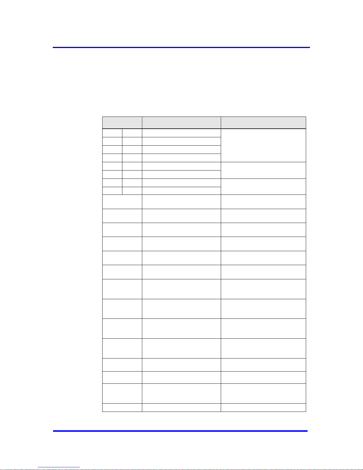
4.2 Control Parameters (Latches/Registers)
These cells can be either read-only or write-only. In the Motorola Mode the
VPC3+C carries out ‘address swapping’ for an access to the address
locations 00H - 07H (word registers). That is, the VPC3+C internally
generates an even address from an odd address and vice-versa.
Address
Intel Mot. Name Bit No. Significance (Read Access!)
00H 01H
Int-Req-Reg 7..0
01H 00H
Int-Req-Reg 15..8
02H 03H
Int−Reg 7..0
03H 02H
Int−Reg 15..8
Interrupt Controller Register
04H 05H
Status-Reg 7..0
05H 04H
Status-Reg 15..8
Status Register
06H 07H
Mode-Reg 0 7..0
07H 06H
Mode-Reg 0 15..8
Mode Register 0
08H Din_Buffer_SM 7..0
Buffer assignment of the
DP_Din_Buffer_State_Machine
09H New_Din_Buffer_Cmd 1..0
The user makes a new DP Din_Buf
available in the N state.
0AH Dout_Buffer_SM 7..0
Buffer assignment of the
DP_Dout_Buffer_State_Machine
0BH Next_Dout_Buffer_Cmd 3..0
The user fetches the last DP
Dout_Buf from the N state
0CH Diag_Buffer_SM 3..0
Buffer assignment for the
DP_Diag_Buffer_State_Machine
0DH New_Diag_Buffer_Cmd 1..0
The user makes a new DP
Diag_Buf available to the VPC3+C.
0EH User_Prm_Data_Okay 1..0
The user positively acknowledges
the user parameter setting data of a
Set_(Ext_)Prm telegram.
0FH User_Prm_Data_Not_Okay 1..0
The user negatively acknowledges
the user parameter setting data of a
Set_(Ext_)Prm telegram.
10H User_Cfg_Data_Okay 1..0
The user positively acknowledges
the configuration data of a Chk_Cfg
telegram.
11H User_Cfg_Data_Not_Okay 1..0
The user negatively acknowledges
the configuration data of a Chk_Cfg
telegram.
12H
DXBout_Buffer_SM 7..0
Buffer assignment of the
DXBout_Buffer_State_Machine
13H
Next_DXBout_Buffer_Cmd 2..0
The user fetches the last
DXBout Buf from the N state
14H SSA_Buffer_Free_Cmd
The user has fetched the data from
the SSA_Buf and enables the buffer
again.
15H
Mode-Reg 1 7..0
Figure 4-2: Assignment of the Internal Parameter-Latches for READ
VPC3+C User Manual
Revision 1.03 15
Copyright © profichip GmbH 2004-2006
Page 16
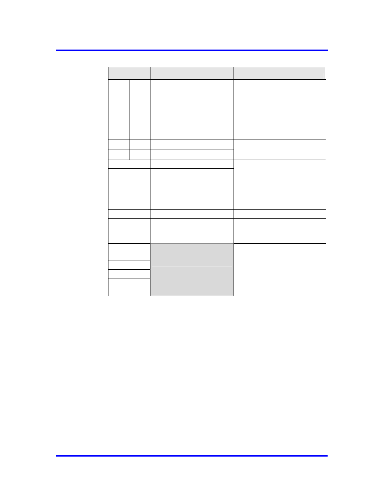
4 Memory Organization
Address
Intel Mot.
Name Bit No. Significance (Write Access!)
00H 01H Int-Req-Reg 7..0
01H
00H Int-Req_Reg 15..8
02H
03H Int-Ack-Reg 7..0
03H
02H Int-Ack-Reg 15..8
04H
05H
Int−Mask-Reg 7..0
05H
04H
Int−Mask-Reg 15..8
Interrupt-Controller-Register
06H
07H Mode-Reg0 7..0
07H
06H Mode-Reg0 15..8
Setting parameters for individual bits
08H
Mode-Reg1-S 7..0
09H
Mode-Reg1-R 7..0
0AH WD_BAUD_CONTROL_Val 7..0
Square-root value for
baud rate monitoring
0BH
minT
SDR
_Val 7..0
minT
SDR
time
0CH
Mode-Reg2 7..0
Mode Register 2
0DH
Sync_PW_Reg 7..0 Sync Pulse Width Register
0EH
Control_Command_Reg 7..0
Control_Command value for
comparison with SYNCH telegram
0FH
Group_Select_Reg 7..0
Group_Select value for comparison
with SYNCH telegram
10H
11H
12H
13H
14H
15H
Reserved
Figure 4-3: Assignment of the Internal Parameter-Latches for WRITE
16 Revision 1.03
VPC3+C
User Manual
Copyright © profichip GmbH 2004-2006
Page 17
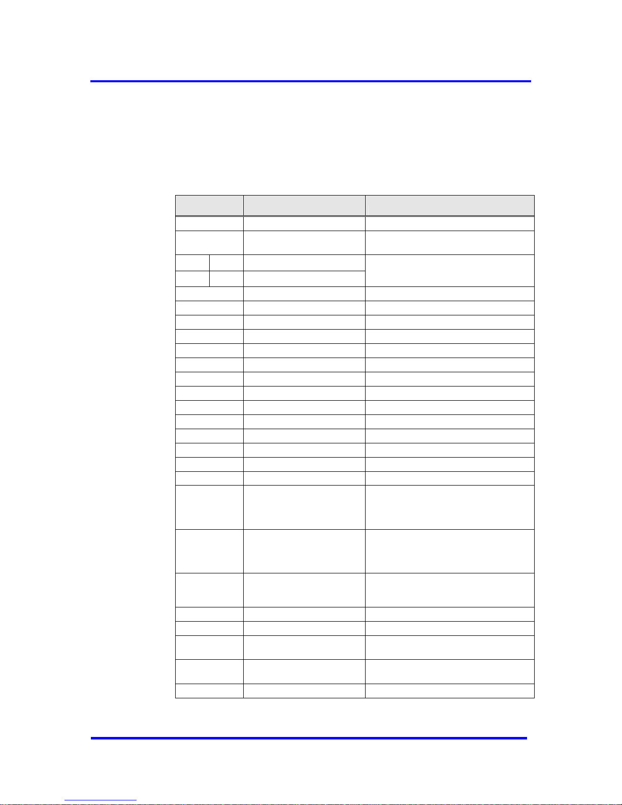
Memory Organization 4
4.3 Organizational Parameters (RAM)
The user stores the organizational parameters in the RAM under the
specified addresses. These parameters can be written and read.
Address
Intel Mot.
Name Bit No. Significance
16H R_TS_Adr Setup Station_Address of the VPC3+C
17H SAP_List_Ptr
Pointer to a RAM address which is preset
with FFh or to SAP-List
18H
19H
R_User_WD_Value 7..0
19H
18H
R_User_WD_Value 15..8
In DP_Mode an internal 16-bit watchdog
timer monitors the user.
1AH R_Len_Dout_Buf Length of the 3 Dout_Buf
1BH R_Dout_Buf_Ptr1 Segment base address of Dout_Buf 1
1CH R_Dout_Buf_Ptr2 Segment base address of Dout_Buf 2
1DH R_Dout_Buf_Ptr3 Segment base address of Dout_Buf 3
1EH R_Len_Din_Buf Length of the 3 Din_Buf
1FH R_Din_Buf_Ptr1 Segment base address of Din_Buf 1
20H R_Din_Buf_Ptr2 Segment base address of Din_Buf 2
21H R_Din_Buf_Ptr3 Segment base address of Din_Buf 3
22H R_Len_DXBout_Buf Length of the 3 DXBout_Buf
23H R_DXBout_Buf_Ptr1 Segment base address of DXBout_Buf 1
24H R_Len Diag_Buf1 Length of Diag_Buf 1
25H R_Len Diag_Buf2 Length of Diag_Buf 2
26H R_Diag_Buf_Ptr1 Segment base address of Diag_Buf 1
27H R_Diag_Buf_Ptr2 Segment base address of Diag_Buf 2
28H R_Len_Cntrl_Buf1
Length of Aux_Buf 1 and the
corresponding control buffer, for example
SSA_Buf, Prm_Buf, Cfg_Buf,
Read_Cfg_Buf
29H R_Len_Cntrl_Buf2
Length of Aux_Buf 2 and the
corresponding control buffer, for example
SSA_Buf, Prm_Buf, Cfg_Buf,
Read_Cfg_Buf
2AH R_Aux_Buf_Sel
Bit array; defines the assignment of the
Aux_Buf 1 and 2 to the control buffers
SSA_Buf, Prm_Buf, Cfg_Buf
2BH R_Aux_Buf_Ptr1 Segment base address of Aux_Buf 1
2CH R_Aux_Buf_Ptr2 Segment base address of Aux_Buf 2
2DH R_Len_SSA_Data
Length of the input data in the
Set_Slave_Address_Buf
2EH R_SSA_Buf_Ptr
Segment base address of the
Set_Slave_Address_Buf
2FH R_Len_Prm_Data Length of the input data in the Prm_Buf
VPC3+C User Manual
Revision 1.03 17
Copyright © profichip GmbH 2004-2006
Page 18

4 Memory Organization
Address
Intel Mot.
Name Bit No. Significance
30H R_Prm_Buf_Ptr Segment base address of the Prm_Buf
31H R_Len_Cfg_Data Length of the input data in the Cfg_Buf
32H R_Cfg_Buf_Ptr Segment base address of the Cfg_Buf
33H
R_Len_Read_Cfg_Data
Length of the input data in the
Read_Cfg_Buf
34H R_Read_Cfg_Buf_Ptr
Segment base address of the
Read_Cfg_Buf
35H R_Len_DXB_Link_Buf Length of the DXB_Linktable
36H R_DXB_Link_Buf_Ptr
Segment base address of the
DXB_Link_Buf
37H R_Len_DXB_Status_Buf Length of the DXB_Status
38H R_DXB_Status_Buf_Ptr
Segment base address of the
DXB_Status_Buf
39H R_Real_No_Add_Change
This parameter specifies whether the
Station_Address may be changed again
later.
3AH R_Ident_Low
The user sets the parameters for the
Ident_Number_Low value.
3BH R_Ident_High
The user sets the parameters for the
Ident_Number_High value.
3CH R_GC_Command
The Control_Command of Global_Control
last received
3DH R_Len_Spec_Prm_Buf
If parameters are set for the
Spec_Prm_Buffer_Mode (see Mode
Register 0), this cell defines the length of
the Prm_Buf.
3EH R_DXBout_Buf_Ptr2 Segment base address of DXBout_Buf 2
3FH R_DXBout_Buf_Ptr3 Segment base address of DXBout_Buf 3
Figure 4-4: Assignment of the Organizational Parameters
18 Revision 1.03
VPC3+C
User Manual
Copyright © profichip GmbH 2004-2006
Page 19
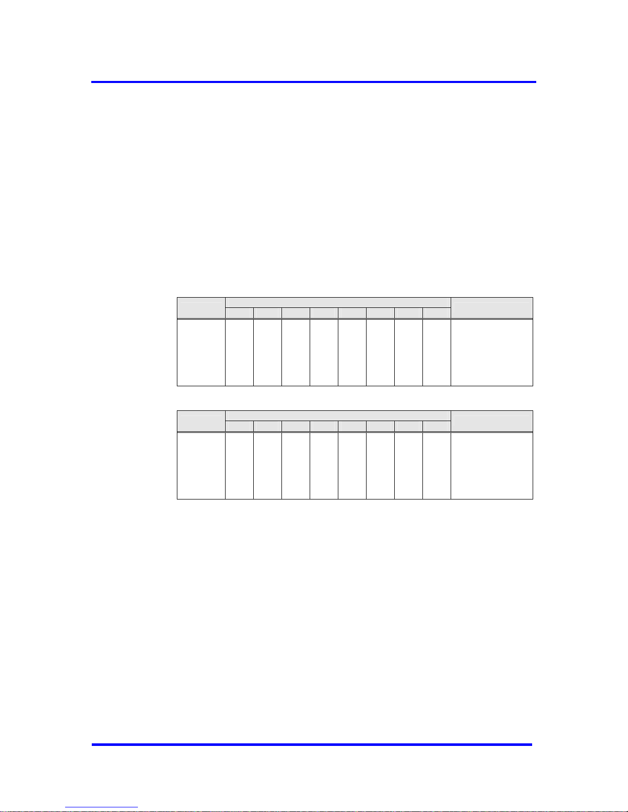
ASIC Interface 5
5 ASIC Interface
5.1 Mode Registers
In the VPC3+C parameter bits that access the controller directly or which
the controller directly sets are combined in three Mode Registers (0, 1 and
2).
5.1.1 Mode Register 0
Setting parameters for Mode Register 0 may take place in the Offline
state only (for example, after power-on). The VPC3+C may not exit the
Offline state until Mode Register 0, all Control and Organizational Parameters are loaded (START_VPC3 = 1 in Mode Register 1).
Bit Position
Address
7 6 5 4 3 2 1 0
Designation
06H
(Intel)
Freeze_
Supported
Sync_
Supported
Early_Rdy
Int_Pol
minT
SDR
WD_Base
Dis_Stop_
Control
Dis_Start_
Control
Mode Reg 0
7 .. 0
See below for
coding
Bit Position
Address
15 14 13 12 11 10 9 8
Designation
07H
(Intel)
Reserved
PrmCmd_
Supported
Spec_Clear_
Mode *)
Spec_Prm_
Buf_Mode **)
Set_Ext_Prm
_Supported
User_Time_
Base
EOI_Time_
Base
DP_Mode
Mode Reg 0
15 .. 8
See below for
coding
*) If Spec_Clear_Mode = 1 (Fail Safe Mode) the VPC3+C will accept Data_Exchange
telegrams without any output data (data unit length = 0) in the state DATA-EXCH. The
reaction to the outputs can be parameterized in the parameterization telegram.
**) When a large number of parameters have to be transmitted from the DP-Master to the
DP-Slave, the Aux-Buffer 1/2 must have the same length as the Parameter-Buffer.
Sometimes this could reach the limit of the available memory in the VPC3+C. When
Spec_Prm_Buf_Mode = 1 the parameterization data are processed directly in this special
buffer and the Aux-Buffers can be held compact.
VPC3+C User Manual
Revision 1.03 19
Copyright © profichip GmbH 2004-2006
Page 20

5 ASIC Interface
Mode Register 0, Low-Byte, Address 06H (Intel):
bit 7
Freeze_Supported: Freeze_Mode support
0 = Freeze_Mode is not supported.
1 = Freeze_Mode is supported
bit 6
Sync_Supported: Sync_Mode support
0 = Sync_Mode is not supported.
1 = Sync_Mode is supported.
bit 5
Early_Rdy: Early Ready
0 = Normal Ready: Ready is generated when data is valid (write) or when data
has been accepted (read).
1 = Ready is generated one clock pulse earlier
bit 4
INT_Pol: Interrupt Polarity
0 = The interrupt output is low-active.
1 = The interrupt output is high-active.
bit 3
minT
SDR
: Default setting for the minT
SDR
after reset for DP operation or
combi operation.
0 = Pure DP operation (default configuration!)
1 = Combi operation
bit 2
WD_Base: Watchdog Time Base
0 = Watchdog time base is 10 ms (default state)
1 = Watchdog time base is 1 ms
bit 1
Dis_Stop_Control: Disable Stopbit Control
0 = Stop bit monitoring is enabled.
1 = Stop bit monitoring is switched off
Set_Prm telegram overwrites this memory cell in the DP_Mode. (Refer to the
user specific data.)
bit 0
Dis_Start_Control: Disable Startbit Control
0 = Monitoring the following start bit is enabled.
1 = Monitoring the following start bit is switched off
Set_Prm telegram overwrites this memory cell in the DP_Mode. (Refer to the
user specific data.)
Figure 5-1: Coding of Mode Register 0, Low-Byte
20 Revision 1.03
VPC3+C
User Manual
Copyright © profichip GmbH 2004-2006
Page 21

ASIC Interface 5
Mode Register 0, High-Byte, Address 07H (Intel):
bit 15
Reserved
bit 14
PrmCmd_Supported: PrmCmd support for redundancy
0 = PrmCmd is not supported.
1 = PrmCmd is supported
bit 13
Spec_Clear_Mode: Special Clear Mode (Fail Safe Mode)
0 = No special clear mode.
1 = Special clear mode. VPC3+C will accept data telegrams with data unit = 0
bit 12
Spec_Prm_Buf_Mode: Special-Parameter-Buffer Mode
0 = No Special-Parameter-Buffer.
1 = Special-Parameter-Buffer mode. Parameterization data will be stored
directly in the Special-Parameter-Buffer.
bit 11
Set_Ext_Prm_Supported: Set_Ext_Prm telegram support
0 = SAP 53 is deactivated
1 = SAP 53 is activated
bit 10
User_Time_Base: Timebase of the cyclical User_Time_Clock-Interrupt
0 = The User_Time_Clock-Interrupt occurs every 1 ms.
1 = The User_Time_Clock-Interrupt occurs every 10 ms.
bit 9
EOI_Time_Base: End-of-Interrupt Timebase
0 = The interrupt inactive time is at least 1 µs long.
1 = The interrupt inactive time is at least 1 ms long
bit 8
DP_Mode: DP_Mode enable
0 = DP_Mode is disabled.
1 = DP_Mode is enabled. VPC3+C sets up all DP_SAPs (default configuration!)
Figure 5-2: Coding of Mode Register 0, High-Byte
5.1.2 Mode Register 1
Some control bits must be changed during operation. These control bits are
combined in Mode Register 1 and can be set independently of each other
(Mode-Reg_1_S) or can be reset independently of each other (ModeReg_1_R). Separate addresses are used for setting and resetting. A logical
‘1’ must be written to the bit position to be set or reset.
For example, to set START_VPC3 write a '1' to address 08H, in order to
reset this bit, write a '1' to address 09H.
VPC3+C User Manual
Revision 1.03 21
Copyright © profichip GmbH 2004-2006
Page 22
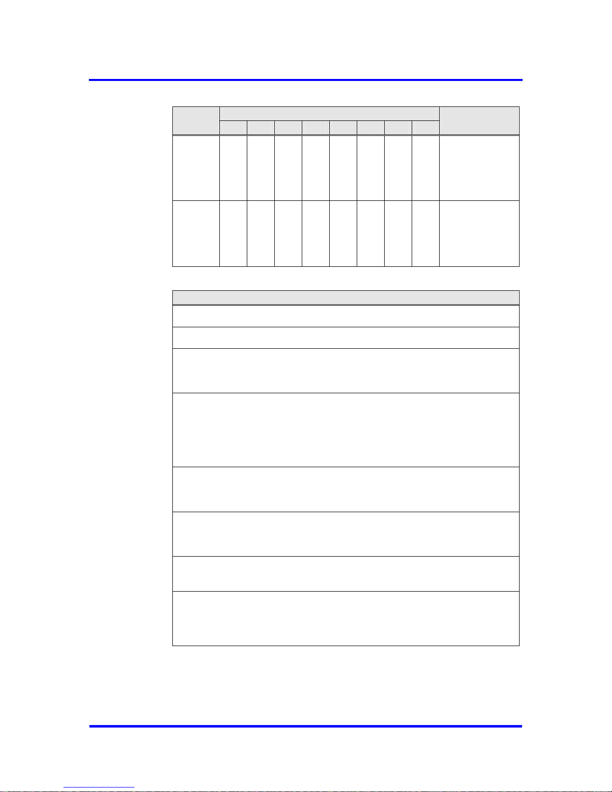
5 ASIC Interface
Bit Position
Address
7 6 5 4 3 2 1 0
Designation
08H
Reserved
Reserved
Res_
User_WD
En_Change_
Cfg_Buffer
User_LEAVE-
MASTER
Go_Offline
EOI
START_
VPC3
Mode-Reg_1_S
7..0
09H
Reserved
Reserved
Res_
User_WD
En_Change_
Cfg_Buffer
User_LEAVE-
MASTER
Go_Offline
EOI
START_
VPC3
Mode-Reg_1_R
7..0
See below
for coding
Mode Register 1, Set, Address 08H:
bit 7
Reserved
bit 6
Reserved
bit 5
Res_User_WD: Resetting the User_WD_Timer
1 = VPC3+C sets the User_WD_Timer to the parameterized value
User_WD_Value. After this action, VPC3+C sets Res_User_WD to ’0'.
bit 4
En_Change_Cfg_Buffer: Enabling buffer exchange (Config-Buffer for
Read_Config-Buffer)
0 = With User_Cfg_Data_Okay_Cmd, the Config-Buffer may not be exchanged
for the Read_Config-Buffer.
1 = With User_Cfg_Data_Okay_Cmd, the Config-Buffer must be exchanged for
the Read_Config-Buffer.
bit 3
User_LEAVE-MASTER. Request to the DP_SM to go to WAIT-PRM.
1 = The user causes the DP_SM to go to WAIT-PRM.
After this action, VPC3+ sets User_LEAVE-MASTER to ’0’ again.
bit 2
Go_Offline: Going into the Offline state
1 = After the current request ends, VPC3+C goes to the Offline state and sets
Go_Offline to ’0’ again.
bit 1
EOI: End-of-Interrupt
1 = VPC3+C disables the interrupt output and sets EOI to ’0‘ again.
bit 0
Start_VPC3: Exiting the Offline state
1 = VPC3+C exits offline and goes to Passive_Idle
In addition the Idle Timer and Watchdog Timer are started and
‘Go_Offline = 0’ is set
Figure 5-3: Coding of Mode Register 1
22 Revision 1.03
VPC3+C
User Manual
Copyright © profichip GmbH 2004-2006
Page 23
ASIC Interface 5
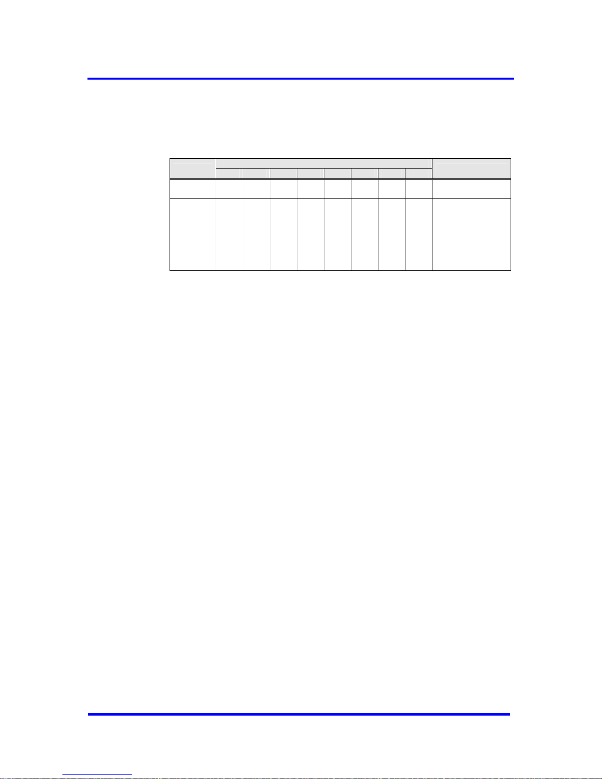
5.1.3 Mode Register 2
Setting parameters for Mode Register 2 may take place in the Offline
State only (like Mode Register 0).
Bit Position
Address
7 6 5 4 3 2 1 0
Designation
0 0 0 0 0 0 0 1
Reset Value
0CH
4kB_Mode
No_Check_
Prm_Reserved
SYNC_Pol
SYNC_Ena
DX_Int_Port
DX_Int_Mode
No_Check_
GC_Reserved
New_GC_
Int_Mode
Mode Reg 2
7 .. 0
VPC3+C User Manual
Revision 1.03 23
Copyright © profichip GmbH 2004-2006
Page 24

5 ASIC Interface
Mode Register 2, Address 0CH:
bit 7
4KB_Mode: size of internal RAM
0 = 2K Byte RAM (default).
1 = 4K Byte RAM
bit 6
No_Check_Prm_Reserved: disables checking of the reserved bits in
DPV1_Status_2/3 of Set_Prm telegram
0 = reserved bits of a Set_Prm telegram are checked (default).
1 = reserved bits of a Set_Prm telegram are not checked.
bit 5
SYNC_Pol: polarity of SYNC pulse (for Isochron Mode only)
0 = negative polarity of SYNC pulse (default)
1 = positive polarity of SYNC pulse
bit 4
SYNC_Ena: enables generation of SYNC pulse (for Isochron Mode only)
0 = SYNC pulse generation is disabled (default)
1 = SYNC pulse generation is enabled
bit 3
DX_Int_Port: Port mode for DX_Out interrupt (ignored if SYNC_Ena set)
0 = DX_Out interrupt is not assigned to port DATAEXCH (default).
1 = DX_Out Interrupt (synchronized to SYNCH telegram) is assigned to port
DATAEXCH.
bit 2
DX_Int_Mode: Mode of DX_out interrupt
0 = DX_Out interrupt is only generated, if Len_Dout_Buf is unequal 0 (default).
1 = DX_Out interrupt is generated after every Data_Exchange telegram
bit 1
No_Check_GC_Reserved: Disables checking of the reserved bits in
Global_Control telegram
0 = reserved bits of a Global_Control telegram are checked (default).
1 = reserved bits of a Global_Control telegram are not checked.
bit 0
GC_Int_Mode: Controls generation of New_GC_Command interrupt
0 = New_GC_Command interrupt is only generated, if a changed
Global_Control telegram is received
1 = New_GC_Command interrupt is generated after every Global_Control
telegram (default)
Figure 5-4: Coding of Mode Register 2
24 Revision 1.03
VPC3+C
User Manual
Copyright © profichip GmbH 2004-2006
Page 25
ASIC Interface 5
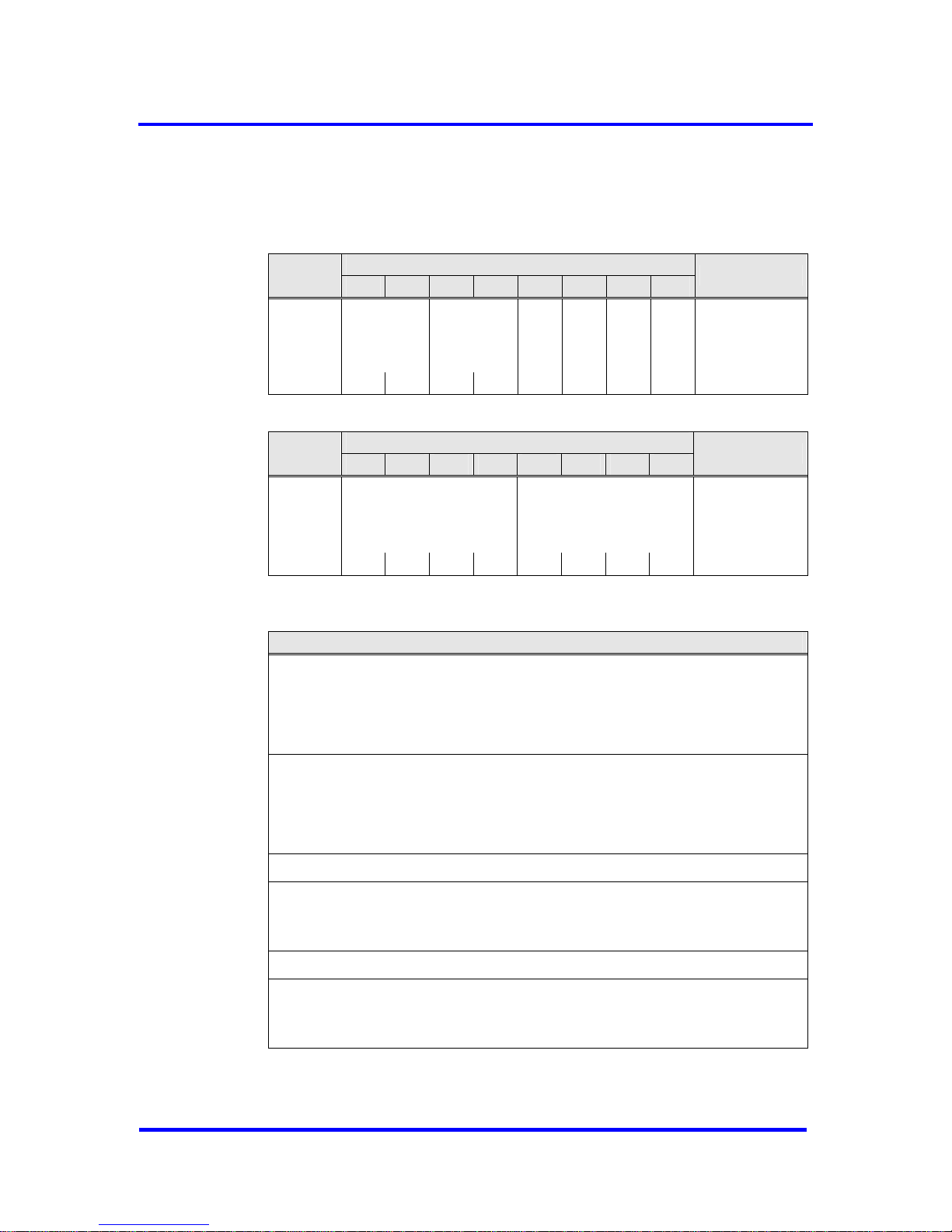
5.2 Status Register
The Status Register shows the current VPC3+C status and can be read
only.
Bit Position
Address
7 6 5 4 3 2 1 0
Designation
WD_State DP_State
04H
(Intel)
1 0 1 0
Reserved
Diag_Flag
Reserved
Offline/
Passive_Idle
Status-Reg
7..0
See below
for coding
Bit Position
Address
15 14 13 12 11 10 9 8
Designation
VPC3+ Release Baud Rate
05H
(Intel)
3 2 1 0 3 2 1 0
Status-Reg
15..8
See below
for coding
Status Register,Low-Byte, Address 04H (Intel):
bit 7,6
WD_State 1..0: State of the Watchdog State Machine
00 = BAUD_SEARCH state
01 = BAUD_CONTROL state
10 = DP_CONTROL state
11 = Not possible
bit 5,4
DP_State 1..0: State of the DP State Machine
00 = WAIT-PRM state
01 = WAIT-CFG state
10 = DATA-EXCH state
11 = Not possible
bit 3
Reserved
bit 2
Diag_Flag: Status of the Diagnosis-Buffer
0 = The Diagnosis-Buffer had been fetched by the DP-Master.
1 = The Diagnosis-Buffer had not been fetched by the DP-Master yet.
bit 1
Reserved
bit 0
Offline/Passive-Idle: Offline-/Passive_Idle state
0 = VPC3+C is in Offline.
1 = VPC3+C is in Passive_Idle.
Figure 5-5: Status Register, Low-Byte
VPC3+C User Manual
Revision 1.03 25
Copyright © profichip GmbH 2004-2006
Page 26

5 ASIC Interface
Status Register, High-Byte, Address 05H (Intel):
bit 15-12
VPC3+-Release 3..0 : Release number for VPC3+
0000 = Step A
1011 = Step B
1100 = Step C
1101 = Step D
Rest = Not possible
bit 11-8
Baud Rate 3..0 : The baud rate found by VPC3+D
0000 = 12,00 Mbit/s
0001 = 6,00 Mbit/s
0010 = 3,00 Mbit/s
0011 = 1,50 Mbit/s
0100 = 500,00 Kbit/s
0101 = 187,50 Kbit/s
0110 = 93,75 Kbit/s
0111 = 45,45 Kbit/s
1000 = 19,20 Kbit/s
1001 = 9,60 Kbit/s
1111 = after reset and during baud rate search
Rest = not possible
Figure 5-6: Status Register, High-Byte
26 Revision 1.03
VPC3+C
User Manual
Copyright © profichip GmbH 2004-2006
Page 27
ASIC Interface 5
5.3 Interrupt Controller
The processor is informed about indication messages and various error
events via the interrupt controller. Up to a total of 16 events are stored in
the interrupt controller. The events are summed up to a common interrupt
output. The controller does not have a prioritization level and does not
provide an interrupt vector (not 8259A compatible!).
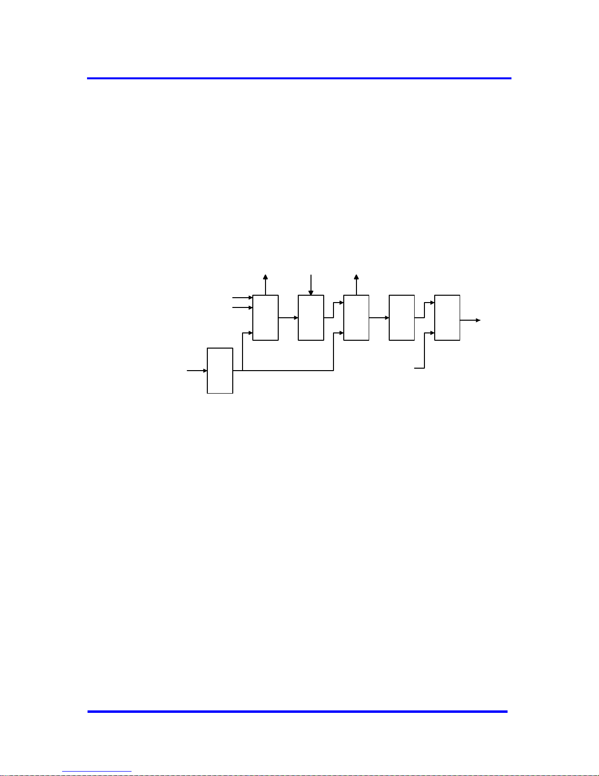
The controller consists of an Interrupt Request Register (IRR), an Interrupt
Mask Register (IMR), an Interrupt Register (IR) and an Interrupt Acknowledge Register (IAR).
IRR
S
R
IMR IR
S
R
IAR
VPC3+
µP
µP
Σ
INT_POL
X/INT
µP µP µP
Figure 5-7: Block Diagram of Interrupt Controller
Each event is stored in the IRR. Individual events can be suppressed via
the IMR. The input in the IRR is independent of the interrupt masks. Events
that are not masked in the IMR set the corresponding IR bit and generate
the X/INT interrupt via a sum network. The user can set each event in the
IRR for debugging.
Each interrupt event that was processed by the microcontroller must be
deleted via the IAR (except for New_(Ext_)Prm_Data and New_Cfg_Data).
A logical ‘1’ must be written on the specific bit position. If a new event and
an acknowledge from the previous event are present at the IRR at the
same time, the event remains stored. If the microcontroller enables a mask
subsequently, it must be ensured that no prior IRR input is present. To be
on the safe side, the position in the IRR must be deleted prior to the
enabling of the mask.
Before leaving the interrupt routine, the microprocessor must set the ‘end of
interrupt bit' (EOI = 1) in Mode Register 1. The interrupt output is switched
to inactive with this edge change. If another event occurs, the interrupt
output is not activated again until the interrupt inactive time of at least 1 µs
or 1 ms expires. This interrupt inactive time can be set via EOI_Time_Base
in Mode Register 0. This makes it possible to enter the interrupt routine
again when an edge-triggered interrupt input is used.
VPC3+C User Manual
Revision 1.03 27
Copyright © profichip GmbH 2004-2006
Page 28
5 ASIC Interface
The polarity of the interrupt output is parameterized via the Int_Pol bit in
Mode Register 0. After hardware reset, the output is low-active.
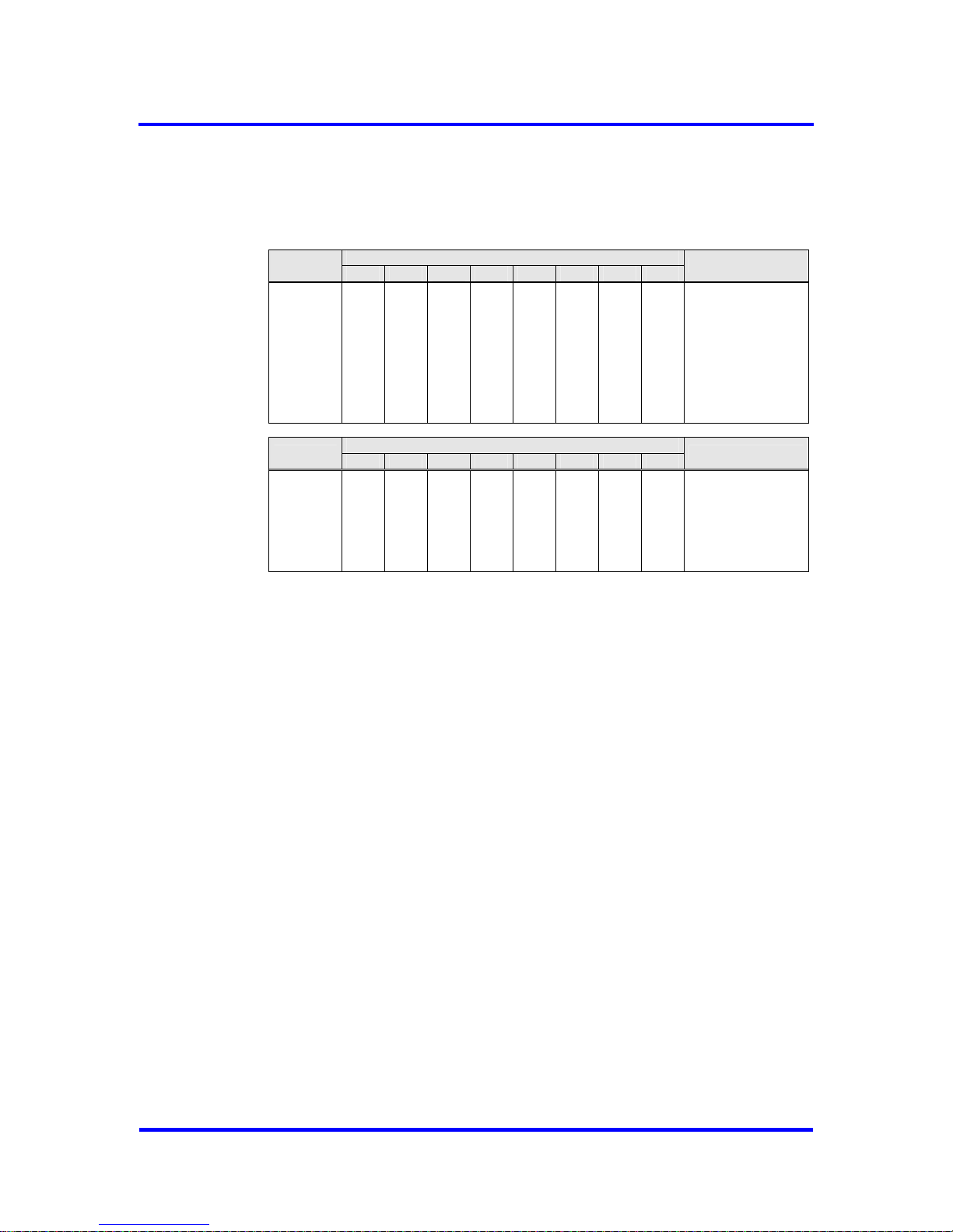
5.3.1 Interrupt Request Register
Bit Position
Address
7 6 5 4 3 2 1 0
Designation
00H
(Intel)
DXB_Out
New_Ext_
Prm_Data
DXB_Link_
Error
User_Timer_
Clock
WD_DP_
CONTROL_Timeout
Baud_Rate_
Detect
Go/Leave_
DATA-EXCH
MAC_Reset
Int-Req-Reg
7 .. 0
See below
for coding
Bit Position
Address
15 14 13 12 11 10 9 8
Designation
01H
(Intel)
FDL_Ind
Poll_End_Ind
DX_Out
Diag_Buffer_
Changed
New_Prm_
Data
New_Cfg_
Data
New_SSA_
Data
New_GC
Command
Int-Req-Reg
15 .. 8
See below
for coding
28 Revision 1.03
VPC3+C
User Manual
Copyright © profichip GmbH 2004-2006
Page 29

ASIC Interface 5
Interrupt-Request-Register, Low-Byte, Address 00H (Intel):
bit 7
DXB_Out:
VPC3+C has received a DXB telegram and made the new output data available
in the ‘N’ buffer.
bit 6
New_Ext_Prm_Data:
The VPC3+C has received a Set_Ext_Prm telegram and made the data
available in the Parameter-Buffer.
bit 5
DXB_Link_Error:
The Watchdog cycle is elapsed and at least one Publisher-Subscriber
connection breaks down.
bit 4
User_Timer_Clock:
The time base for the User_Timer_Clocks is run out (1 / 10ms).
bit 3
WD_DP_CONTROL_Timeout:
The watchdog timer expired in the DP_CONTROL state.
bit 2
Baud_Rate_Detect:
The VPC3+C has left the BAUD_SEARCH state and found a baud rate.
bit 1
Go/Leave_DATA-EXCH:
The DP_SM has entered or exited the DATA-EXCH state.
bit 0
MAC_Reset:
After processing the current request, the VPC3+C has entered the Offline state
(by setting the Go_Offline bit).
Figure 5-8: Interrupt-Request-Register, Low-Byte
VPC3+C User Manual
Revision 1.03 29
Copyright © profichip GmbH 2004-2006
Page 30

5 ASIC Interface
Interrupt Request Register 0, High-Byte, Address 01H (Intel):
bit 15
FDL_Ind:
The VPC3+C has received an acyclic service request and made the data
available in an Indication-Buffer.
bit 14
Poll_End_Ind:
The VPC3+C have send the response to an acyclic service.
bit 13
DX_Out:
The VPC3+C have received a Data_Exchange telegram and made the new
output data available in the ‘N’ buffer.
bit 12
Diag_Buffer_Changed:
Due to the request made by New_Diag_Cmd, the VPC3+C exchanged the
Diagnosis-Buffers and made the old buffer available to the user again.
bit 11
New_Prm_Data:
The VPC3+C have received a Set_Prm telegram and made the data available
in the Parameter-Buffer.
bit 10
New_Cfg_Data:
The VPC3+C have received a Chk_Cfg telegram and made the data available
in the Config-Buffer.
bit 9
New_SSA_Data:
The VPC3+C have received a Set_Slave_Add telegram and made the data
available in the Set_Slave_Add-Buffer.
bit 8
New_GC_Command:
The VPC3+C have received a Global_Control telegram and stored the
Control_Command in the R_GC_Command RAM cell.
Figure 5-9: Interrupt Request Register, High-Byte
30 Revision 1.03
VPC3+C
User Manual
Copyright © profichip GmbH 2004-2006
Page 31
ASIC Interface 5
5.3.2 Interrupt Acknowledge / Mask Register
The other interrupt controller registers are assigned in the bit positions like
the Interrupt Request Register.
Address Register Reset state Assignment
02H / 03H Interrupt
Register (IR)
Readable only All bits
cleared
04H / 05H Interrupt
Mask
Register
(IMR)
Writeable, can
be changed
during operation
All bits set 1 = Mask is set and the
interrupt is disabled
0 = Mask is cleared and the
interrupt is enabled
02H / 03H Interrupt
Acknowledge
Register
(IAR)
Writeable, can
be changed
during operation
All bits
cleared
1 = Interrupt is
acknowledged and the IRR
bit is cleared
0 = IRR bit remains
unchanged
Figure 5-10: Interrupt Acknowledge / Mask Register
The New_(Ext_)Prm_Data, New_Cfg_Data interrupts cannot be
acknowledged via the Interrupt Acknowledge Register. The relevant state
machines clear these interrupts through the user acknowledgements (for
example, User_Prm_Data_Okay etc.).
5.4 Watchdog Timer
The VPC3+C is able to identify the baud rate automatically. The state machine is in the BAUD_SEARCH state after each RESET and also after the
Watchdog (WD) Timer has expired in the BAUD_CONTROL state.
BAUD_CONTROL
DP_CONTROL
BAUD_SEARCH
WD_Timeout
baudrate detected
WD_On = 1
WD_On = 0
or
WD_DP_CONTROL_Timeout
Figure 5-11: Watchdog State Machine (WD_SM)
VPC3+C User Manual
Revision 1.03 31
Copyright © profichip GmbH 2004-2006
Page 32

5 ASIC Interface
5.4.1 Automatic Baud Rate Identification
The VPC3+C starts searching for the transmission rate using the highest
baud rate. If no SD1 telegram, SD2 telegram, or SD3 telegram was
received completely and without errors during the monitoring time, the
search continues using the next lower baud rate.
After identifying the correct baud rate, the VPC3+C switches to the
BAUD_CONTROL state and observes the baud rate. The monitoring time
can be parameterized (WD_BAUD_CONTROL_Val). The watchdog uses a
clock of 100 Hz (10 ms). Each telegram to its own Station_Address
received with no errors resets the Watchdog. If the timer expires, the
VPC3+C switches to the BAUD_SEARCH state again.
5.4.2 Baud Rate Monitoring
The detected baud rate is permanently monitored in BAUD_CONTROL.
The Watchdog is triggered by each error-free telegram to its own
Station_Address. The monitoring time results from multiplying twice
WD_BAUD_CONTROL_Val (user sets this parameter) by the time base (10
ms). If the timer expires, WD_SM again goes to BAUD_SEARCH. If the
user uses the DP protocol (DP_Mode = 1, see Mode Register 0), the
watchdog is used for the DP_CONTROL state, after a Set_Prm telegram
was received with an enabled response time monitoring (WD_On = 1). The
watchdog timer remains in the baud rate monitoring state when the master
monitoring is disabled (WD_On = 0). The DP_SM is not reset when the
timer expires in the state BAUD_CONTROL. That is, the DP-Slave remains
in the DATA-EXCH state, for example.
5.4.3 Response Time Monitoring
The DP_CONTROL state serves as the response time monitoring of the
DP-Master (Diag_Master_Add). The used monitoring time results from
multiplying both watchdog factors and then multiplying this result with the
time base (1 ms or 10 ms):
T
WD
= WD_Base * WD_Fact_1 * WD_Fact_2
(See byte 7 of the Set_Prm telegram.)
The user can load the two watchdog factors (WD_Fact_1 and WD_Fact_2)
and the time base that represents a measurement for the monitoring time
via the Set_Prm telegram with any value between 1 and 255.
EXCEPTION:
The WD_Fact_1 = WD_Fact_2 = 1 setting is not allowed. The circuit
does not check this setting.
A monitoring time between 2 ms and 650 s - independent of the baud rate can be implemented with the allowed watchdog factors.
32 Revision 1.03
VPC3+C
User Manual
Copyright © profichip GmbH 2004-2006
Page 33

ASIC Interface 5
If the monitoring time expires, the VPC3+C goes to BAUD_CONTROL state
again and generates the WD_DP_CONTROL_Timeout interrupt. In
addition, the DP State Machine is reset, that is, it generates the reset states
of the buffer management. This operation mode is recommended for the
most applications.
If another DP-Master takes over the VPC3+C, the Watchdog State Machine
either branches to BAUD_CONTROL (WD_On = 0) or to DP_CONTROL
(WD_On = 1).
VPC3+C User Manual
Revision 1.03 33
Copyright © profichip GmbH 2004-2006
Page 34

5 ASIC Interface
Notes:
34 Revision 1.03
VPC3+C
User Manual
Copyright © profichip GmbH 2004-2006
Page 35

PROFIBUS DP Interface 6
6 PROFIBUS DP Interface
6.1 DP Buffer Structure
The DP_Mode is enabled in the VPC3+C with ‘DP_Mode = 1’ (see Mode
Register 0). In this mode, the following SAPs are permanently reserved:
Default SAP: Write and Read data (Data_Exchange)
SAP 53: Sending extended parameter setting data (Set_Ext_Prm)
SAP 55: Changing the Station_Address (Set_Slave_Add)
SAP 56: Reading the inputs (RD_Input)
SAP 57: Reading the outputs (RD_Output)
SAP 58: Control commands to the DP-Slave (Global_Control)
SAP 59: Reading configuration data (Get_Cfg)
SAP 60: Reading diagnosis information (Slave_Diag)
SAP 61: Sending parameter setting data (Set_Prm)
SAP 62: Checking configuration data (Chk_Cfg)
The DP-Slave protocol is completely integrated in the VPC3+C and is
handled independently. The user must correspondingly parameterize the
ASIC and process and acknowledge received messages. All SAPs are
always enabled except the Default SAP, SAP 56, SAP 57 and SAP 58. The
remaining SAPs are not enabled until the DP_SM goes into the DATAEXCH state. The user can disable SAP 55 to not permit changing the
Station_Address. The corresponding buffer pointer R_SSA_Buf_Ptr must
be set to ‘00H’ for this purpose.
The DP_SAP Buffer Structure is shown in Figure 6-1. The user configures
all buffers (length and buffer start) in the Offline state. During operation, the
buffer configuration must not be changed, except for the length of the Dout/Din-Buffers.
The user may still adapt these buffers in the WAIT-CFG state after the configuration telegram (Chk_Cfg). Only the same configuration may be
accepted in the DATA-EXCH state.
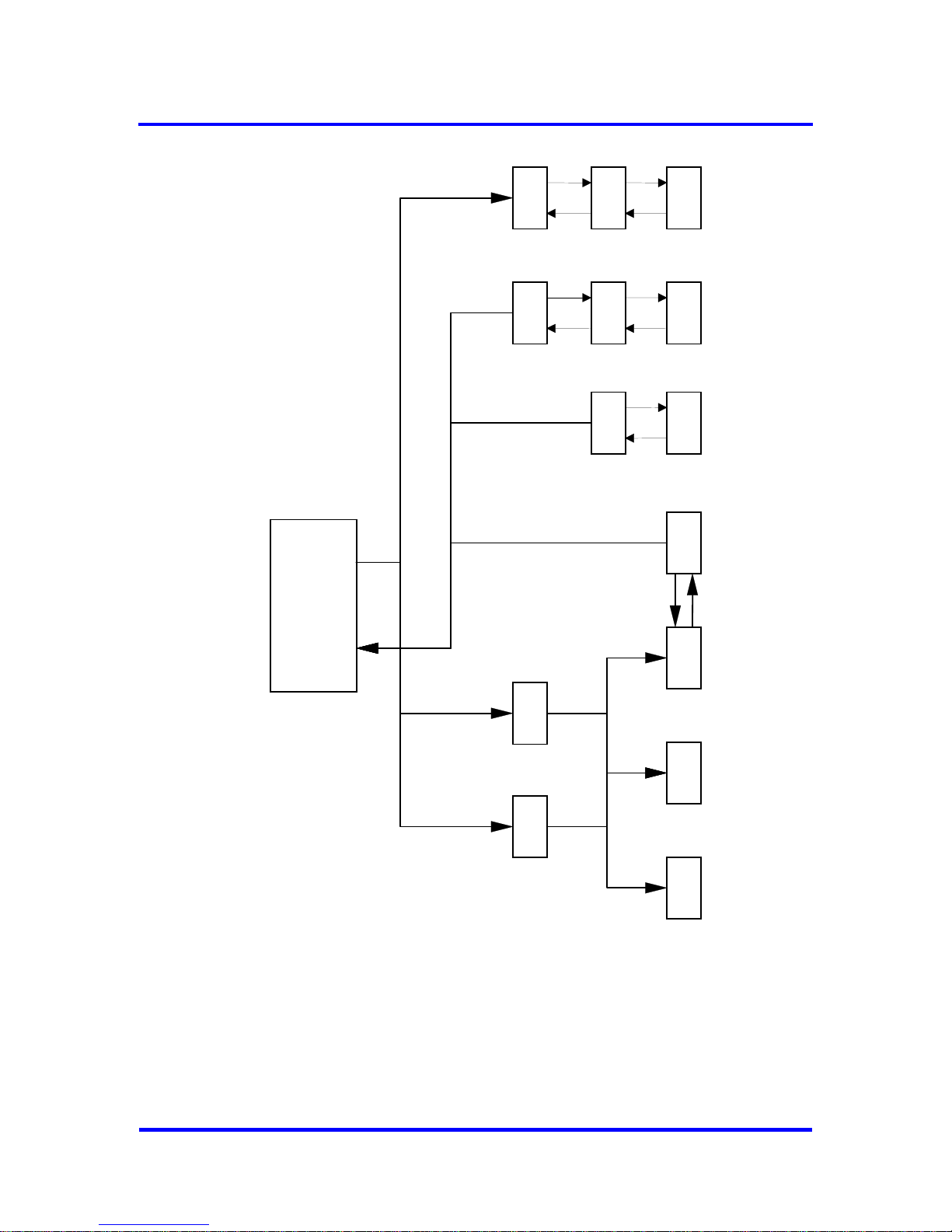
The buffer structure is divided into the data buffers, Diagnosis-Buffers and
the control buffers. Both the output data and the input data have three
buffers available with the same length. These buffers are working as
changing buffers. One buffer is assigned to the ‘D’ data transfer and one
buffer is assigned to the ‘U’ user. The third buffer is either in a next state 'N'
or a free state ‘F’. One of the two states is always unoccupied.
For diagnosis two Diagnosis-Buffers, that can have different lengths, are
available. One Diagnosis-Buffer (D) is always assigned to the VPC3+C for
sending. The other Diagnosis-Buffer (U) belongs to the user for
preprocessing new diagnosis data.
VPC3+C User Manual
Revision 1.03 35
Copyright © profichip GmbH 2004-2006
Page 36
6 PROFIBUS DP Interface
D N U
D N U
D U
A
ux
1/2
A
ux
1/2
UART
Dout-Buffer
Din-Buffer
DiagnosisBuffer
Read_ConfigBuffer
Config-Buffer
Set-Slave-
A
ddress-Buffer
ParameterBuffer
D-N changed
by VPC3+
N-U changed
by User
changed by User
Figure 6-1: DP_SAP Buffer Structure
The VPC3+C first stores the parameter telegrams (Set_Slave_Add and
Set_(Ext_)Prm) and the configuration telegram (Chk_Cfg) in Aux-Buffer 1
or Aux-Buffer 2. If the telegrams are error-free, data is exchanged with the
corresponding target buffer (Set_Slave_Add-Buffer, Parameter-Buffer and
Config-Buffer). Each of the buffers to be exchanged must have the same
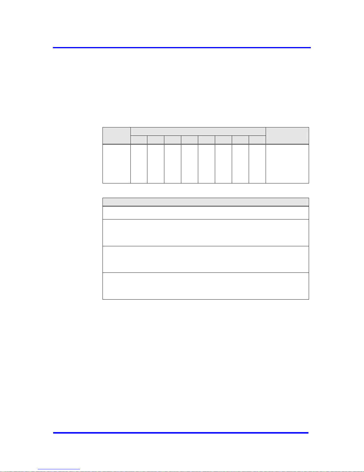
length. In the R_Aux_Buf_Sel parameter cell (see Figure 6-2) the user
defines which Aux_buffers are to be used for the telegrams mentioned
36 Revision 1.03
VPC3+C
User Manual
Copyright © profichip GmbH 2004-2006
Page 37
PROFIBUS DP Interface 6
above. The Aux-Buffer 1 must always be available, Aux-Buffer 2 is optional.
If the data profiles of these DP telegrams are very different (for example the
length of the Set_Prm telegram is significantly larger than the length of the
other telegrams) it is suggested to make an Aux-Buffer 2 available
(R_Aux_Buf_Sel: Set_Prm = 1) for this telegram. The other telegrams are
then read via Aux-Buffer 1 (R_Aux_Buf_Sel: Set_Slave_Adr = 0, Chk_Cfg
= 0). If the buffers are too small, the VPC3+C responds with “no resources”
(RR)!
Bit Position
Address
7 6 5 4 3 2 1 0
Designation
2AH
0 0 0 0 0
Set_
Slave_Add
Chk_Cfg
Set_Prm
R_Aux_Buf_Sel
See below
for coding
R_Aux_Buf_Sel, Address 2AH:
bit 7-3
Don’t Care: Read as ‘0’
bit 2
Set_Slave_Adr: Set Slave Address
0 = Aux-Buffer 1
1 = Aux-Buffer 2
bit 1
Chk_Cfg: Check Configuration
0 = Aux-Buffer 1
1 = Aux-Buffer 2
bit 0
Set_Prm: Set (Extended) Parameter
0 = Aux-Buffer 1
1 = Aux-Buffer 2
Figure 6-2: Aux-Buffer Management
The user makes the configuration data (Get_Cfg) available in the
Read_Config-Buffer for reading. The Read_Config-Buffer must have the
same length as the Config-Buffer.
The RD_Input telegram is serviced from the Din-buffer in the ‘D’ state and
the RD_Output telegram is serviced from the Dout-Buffer in the ‘U’ state.
All buffer pointers are 8-bit segment addresses, because the VPC3+C have
only 8-bit address registers internally. For a RAM access, VPC3+C adds an
8-bit offset address to the segment address shifted by 4 bits (result: 12-bit
physical address) in case of 4K Byte RAM or shifted by 3 bits (result: 11- bit
physical address) in case of 2K Byte RAM. With regard to the buffer start
addresses, this specification results either in a 16-byte or in an 8-byte
granularity.
VPC3+C User Manual
Revision 1.03 37
Copyright © profichip GmbH 2004-2006
Page 38
6 PROFIBUS DP Interface
6.2 Description of the DP Services
6.2.1 Set_Slave_Add (SAP 55)
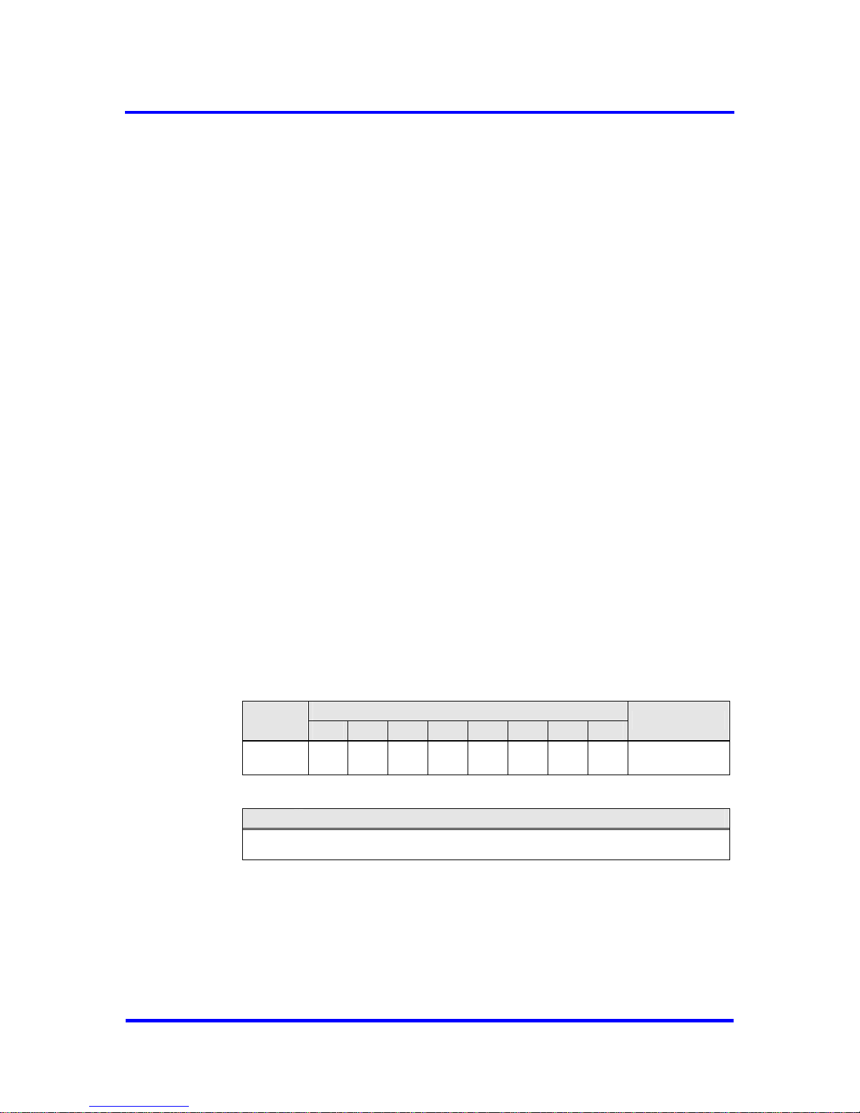
Sequence for the Set_Slave_Add service
The user can disable this service by setting ‘R_SSA_Puf_Ptr = 00H’. The
Station_Address must then be determined, for example, by reading a DIPswitch or an EEPROM and writing the address in the RAM cell R_TS_Adr.
There must be a non-volatile memory available (for example an external
EEPROM) to support this service. It must be possible to store the
Station_Address and the Real_No_Add_Change (‘True’ = FFH) parameter
in this EEPROM. After each restart caused by a power failure, the user
must read these values from the EEPROM again and write them to the
R_TS_Adr und R_Real_No_Add_Change RAM registers.
If SAP55 is enabled and the Set_Slave_Add telegram is received correctly,
the VPC3+C enters the pure data in the Aux-Buffer 1/2, exchanges the
Aux-Buffer 1/2 for the Set_Slave_Add-Buffer, stores the entered data
length in R_Len_SSA_Data, generates the New_SSA_Data interrupt and
internally stores the New_Slave_Add as Station_Address and the
No_Add_Chg as Real_No_Add_Chg. The user does not need to transfer
this changed parameter to the VPC3+C again. After reading the buffer, the
user generates the SSA_Buffer_Free_Cmd (read operation on address
14H). This makes the VPC3+C ready again to receive another
Set_Slave_Add telegram (for example, from a different DP-Master).
The VPC3+C reacts automatically to errors.
Bit Position
Address
7 6 5 4 3 2 1 0
Designation
14H 0 0 0 0 0 0 0 0
SSA_Buf_
Free_Cmd
SSA_Buf_Free_Cmd, Address 14H:
bit 7-0
Don’t care: Read as ‘0’
Figure 6-3: Coding of SSA_Buffer_Free_Command
38 Revision 1.03
VPC3+C
User Manual
Copyright © profichip GmbH 2004-2006
Page 39
PROFIBUS DP Interface 6
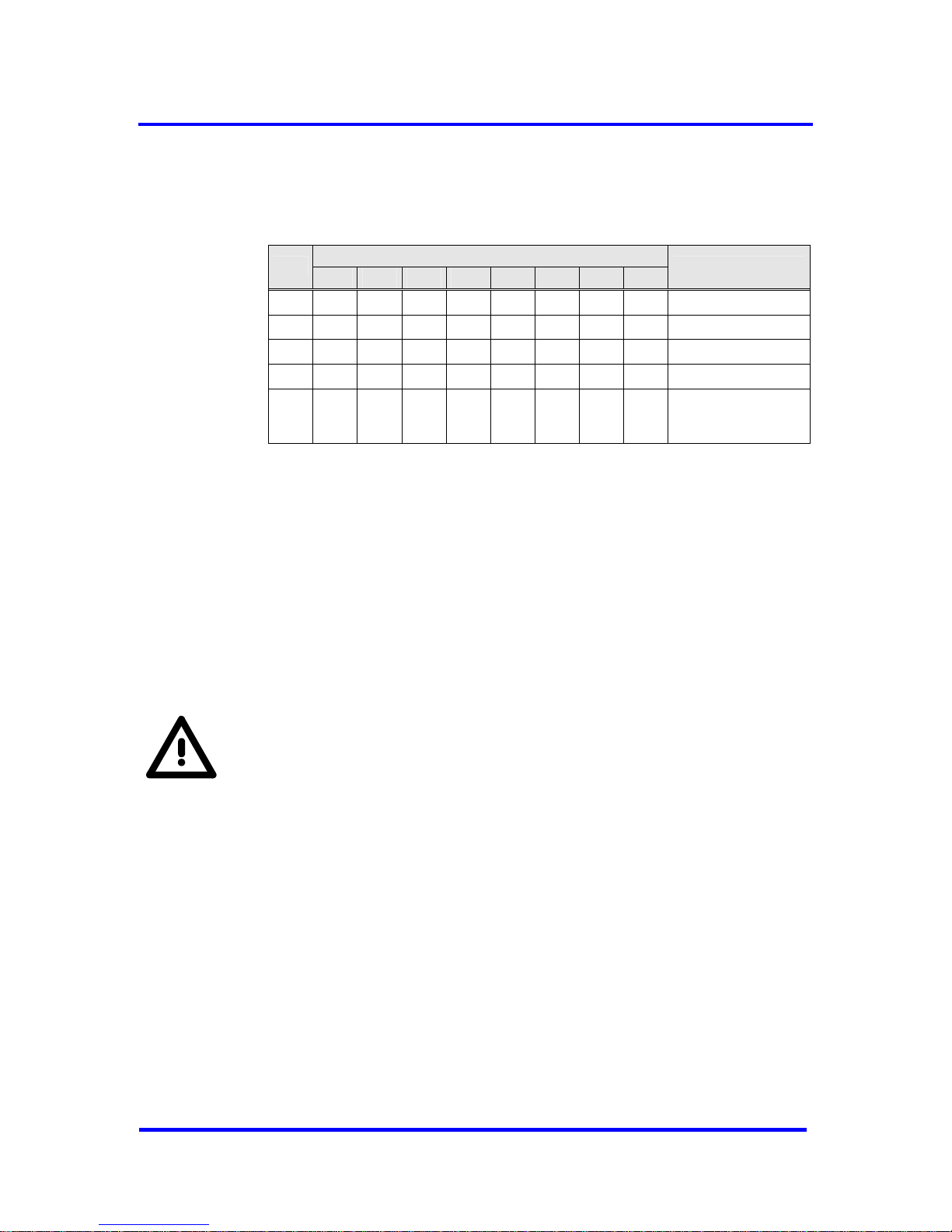
Structure of the Set_Slave_Add Telegram
The net data are stored as follows in the SSA buffer:
Bit Position
Byte
7 6 5 4 3 2 1 0
Designation
0 New_Slave_Address
1 Ident_Number_High
2 Ident_Number_Low
3 No_Add_Chg
4
:
243
Rem_Slave_Data
additional application
specific data
Figure 6-4: Structure of the Set_Slave_Add Telegram
6.2.2 Set _Prm (SAP 61)
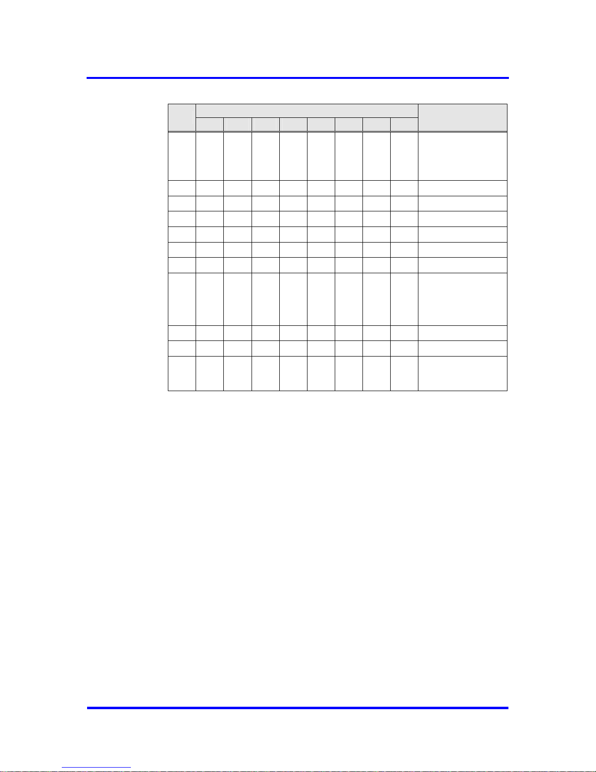
Parameter Data Structure
The VPC3+C evaluates the first seven data bytes (without
User_Prm_Data), or the first eight data bytes (with User_Prm_Data). The
first seven bytes are specified according to the standard. The eighth byte is
used for VPC3+C specific characteristics. The additional bytes are
available to the application.
If a PROFIBUS DP extension shall be used, the bytes 7-9 are called
DPV1_Status and must be coded as described in section 7,
“PROFIBUS DP Extensions”. Generally it is recommended to start the
User_Prm_Data first with byte 10.
VPC3+C User Manual
Revision 1.03 39
Copyright © profichip GmbH 2004-2006
Page 40
6 PROFIBUS DP Interface
Bit Position
Byte
7 6 5 4 3 2 1 0
Designation
0
Lock_
Req
Unlock_
Req
Sync_
Req
Freeze_
Req
WD_On
Reserved
Reserved
Reserved
Station Status
1 WD_Fact_1
2 WD_Fact_2
3 minT
SDR
4 Ident_Number_High
5 Ident_Number_Low
6 Group_Ident
7
DPV1_
Enable
Fail_Safe
Publisher_
Enable
0 0
WD_Base
Dis_Stop_
Control
Dis_Start_
Control
Spec_User_Prm_Byte
/DPV1_Status_1
8 DPV1_Status_2
9 DPV1_Status_3
10
:
243
User_Prm_Data
Figure 6-5: Format of the Set_Prm Telegram
40 Revision 1.03
VPC3+C
User Manual
Copyright © profichip GmbH 2004-2006
Page 41
PROFIBUS DP Interface 6
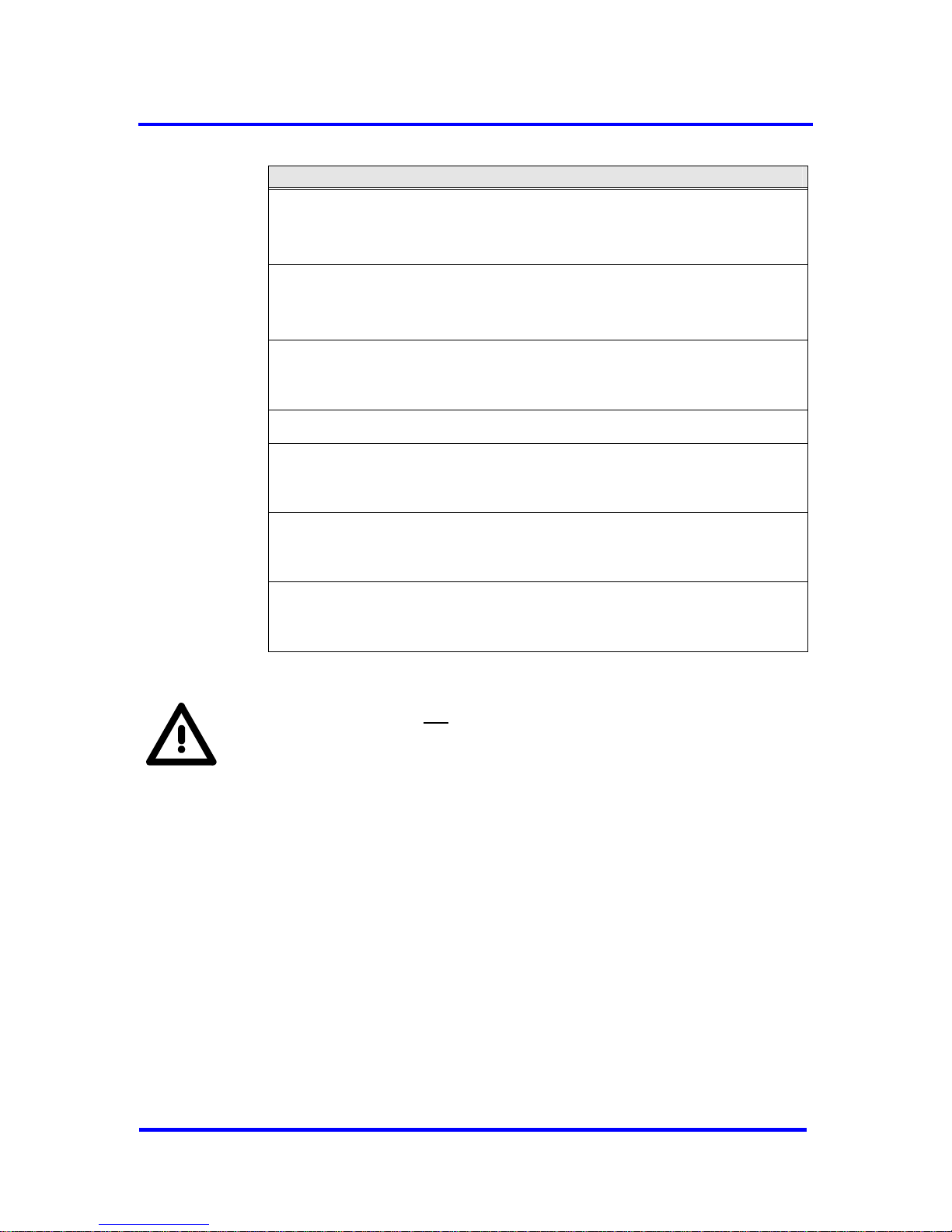
Spec_User_Prm_Byte / DPV1_Status_1:
bit 7
DPV1_Enable:
0 = DP-V1 extensions disabled (default)
1 = DP-V1 extensions enabled
bit 6
Fail_Safe:
0 = Fail Safe mode disabled (default)
1 = Fail Safe mode enabled
bit 5
Publisher_Enable:
0 = Publisher function disabled (default)
1 = Publisher function enabled
bit 4-3
Reserved: To be parameterized with ‘0’
bit 2
WD_Base: Watchdog Time Base
0 = Watchdog time base is 10 ms (default)
1 = Watchdog time base is 1 ms
bit 1
Dis_Stop_Control: Disable Stop bit Control
0 = Stop bit monitoring in the receiver is enabled (default)
1 = Stop bit monitoring in the receiver is disabled
bit 0
Dis_Start_Control: Disable Start bit Control
0 = Start bit monitoring in the receiver is enabled (default)
1 = Start bit monitoring in the receiver is disabled
Figure 6-6: Spec_User_Prm_Byte / DPV1_Status_1
It is recommended
not to use the DPV1_Status bytes (bytes 7-9) for
user parameter data.
VPC3+C User Manual
Revision 1.03 41
Copyright © profichip GmbH 2004-2006
Page 42
6 PROFIBUS DP Interface
Parameter Data Processing Sequence
In the case of a positive validation of more than seven data bytes, the
VPC3+C carries out the following reaction:
The VPC3+C exchanges Aux-Buffer 1/2 (all data bytes are entered here)
for the Parameter-Buffer, stores the input data length in R_Len_Prm_Data
and triggers the New_Prm_Data interrupt. The user must then check the
User_Prm_Data and either reply with User_Prm_Data_Okay_Cmd or with
User_Prm_Data_Not_Okay_Cmd. The entire telegram is entered in this
buffer. The user parameter data are stored beginning with data byte 8, or
with byte 10 if DPV1_Status bytes used.
The user response (User_Prm_Data_Okay_Cmd or User_Prm_Data_Not_Okay_Cmd) clears the New_Prm_Data interrupt. The user cannot
acknowledge the New_Prm_Data interrupt in the IAR register.
With the User_Prm_Data_Not_Okay_Cmd message, relevant diagnosis
bits are set and the DP_SM branches to WAIT-PRM.
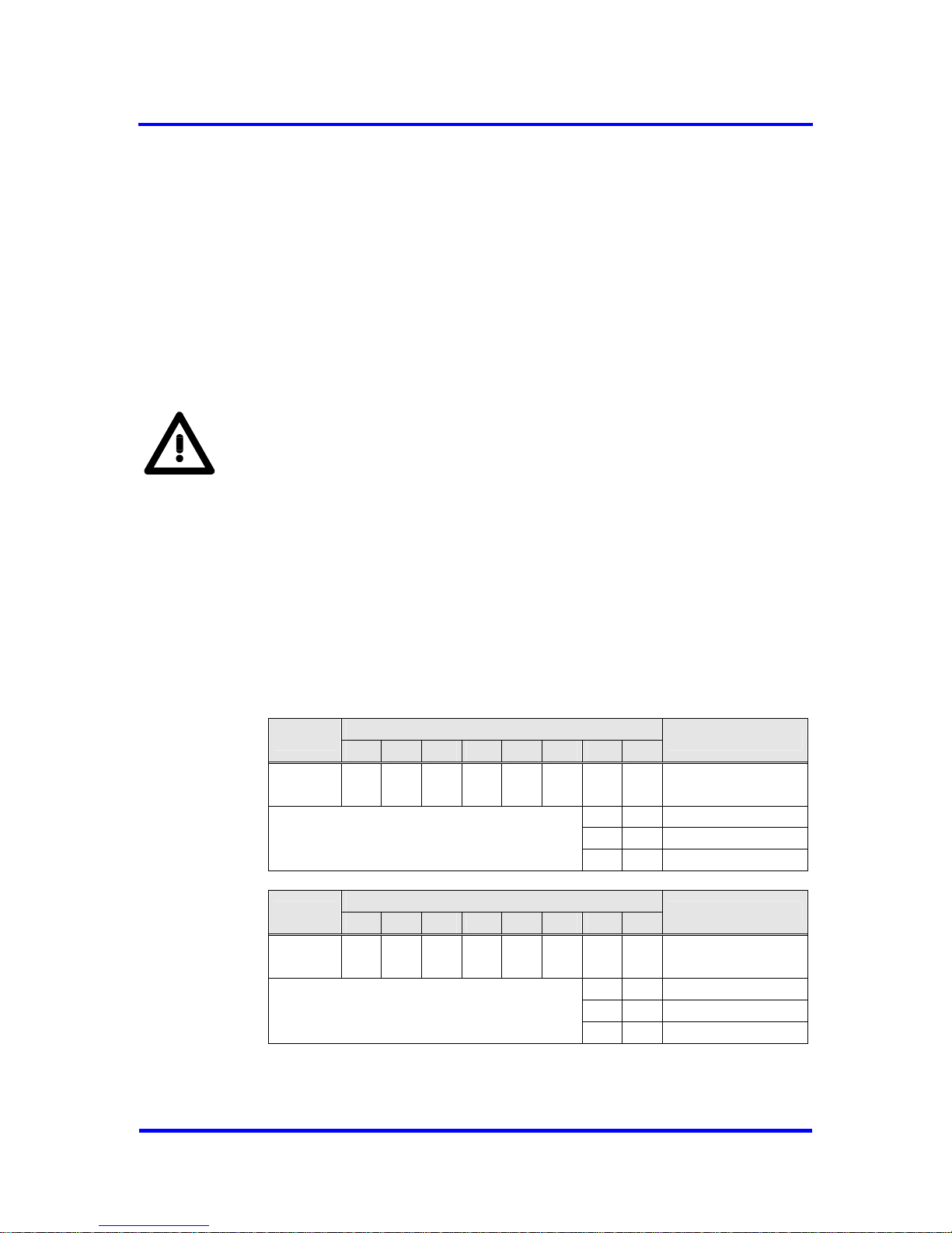
The User_Prm_Data_Okay and User_Prm_Data_Not_Okay acknowledgements are read accesses to defined registers with the relevant signals:
• User_Prm_Finished:
No additional parameter telegram is present.
• Prm_Conflict:
An additional parameter telegram is present,
processing again
• Not_Allowed:
Access not permitted in the current bus state
Bit Position
Address
7 6 5 4 3 2 1 0
Designation
0EH 0 0 0 0 0 0
⇓ ⇓
User_Prm_
Data_Okay
0 0 User_Prm_Finished
0 1 Prm_Conflict
1 1 Not_Allowed
Bit Position
Address
7 6 5 4 3 2 1 0
Designation
0FH 0 0 0 0 0 0
⇓ ⇓
User_Prm_
Data_Not_Okay
0 0 User_Prm_Finished
0 1 Prm_Conflict
1 1 Not_Allowed
Figure 6-7: Coding of User_Prm_(Not)_Okay_Cmd
42 Revision 1.03
VPC3+C
User Manual
Copyright © profichip GmbH 2004-2006
Page 43

PROFIBUS DP Interface 6
If another Set_Prm telegram is supposed to be received in the meantime,
the signal Prm_Conflict is returned for the positive or negative
acknowledgement of the first Set_Prm telegram. Then the user must repeat
the validation because the VPC3+C has made a new Parameter-Buffer
available.
6.2.3 Chk_Cfg (SAP 62)
The user checks the correctness of the configuration data. After receiving
an error-free Chk_Cfg telegram, the VPC3+C exchanges the Aux-Buffer 1/2
(all data bytes are entered here) for the Config-Buffer, stores the input data
length in R_Len_Cfg_Data and generates the New_Cfg_Data interrupt.
Then the user has to check the User_Config_Data and either respond with
User_Cfg_Data_Okay_Cmd or with User_Cfg_Data_Not_Okay_Cmd. The
pure data is entered in the buffer in the format of the standard.
The user response (User_Cfg_Data_Okay_Cmd or the
User_Cfg_Data_Not_Okay_Cmd response) clears the New_Cfg_Data
interrupt. The user cannot acknowledge the New_Cfg_Data in the IAR
register.
If an incorrect configuration is reported, several diagnosis bits are changed
and the VPC3+C branches to state WAIT-PRM.
For a correct configuration, the transition to DATA-EXCH takes place
immediately, if trigger counters for the parameter telegrams and
configuration telegrams are at 0. When entering into DATA-EXCH, the
VPC3+C also generates the Go/Leave_DATA-EXCH Interrupt.
If the received configuration data from the Config-Buffer is supposed to
result in a change to the Read_Config-Buffer (contains the data for the
Get_Cfg telegram), the user have to make the new Read_Config data
available in the Read_Config-Buffer before the User_Cfg_Data_Okay_Cmd
acknowledgement, that is the user has to copy the new configuration data
into the Read_Config-Buffer.
During acknowledgement, the user receives information about whether
there is a conflict or not. If another Chk_Cfg telegram was supposed to be
received in the meantime, the user receives the Cfg_Conflict signal during
the positive or negative acknowledgement of the first Chk_Cfg telegram.
Then the user must repeat the validation, because the VPC3+C have made
a new Config-Buffer available.
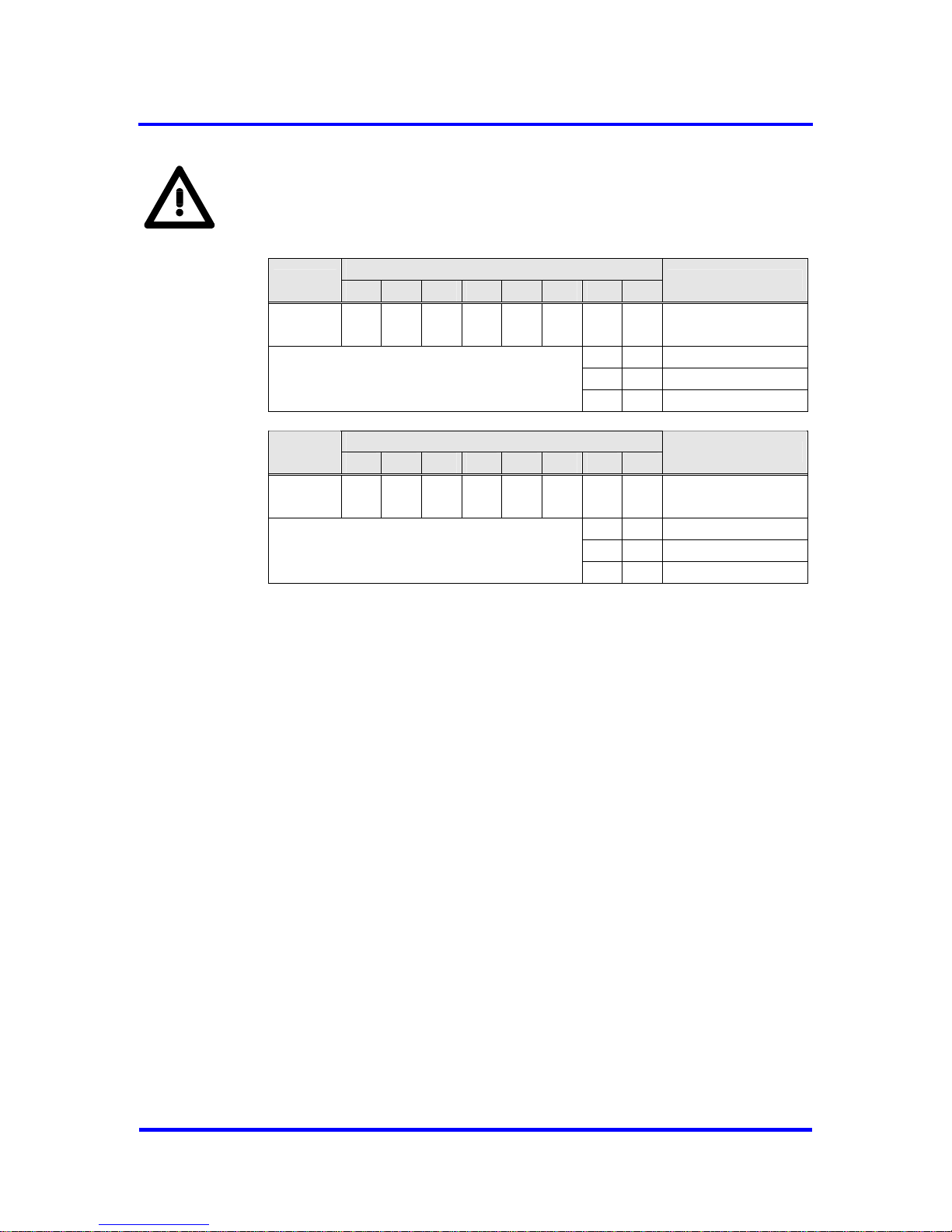
The User_Cfg_Data_Okay_Cmd and User_Cfg_Data_Not_Okay_Cmd
acknowledgements are read accesses to defined memory cells with the
relevant Not_Allowed, User_Cfg_Finished, or Cfg_Conflict signals.
VPC3+C User Manual
Revision 1.03 43
Copyright © profichip GmbH 2004-2006
Page 44
6 PROFIBUS DP Interface
If the New_Prm_Data and New_Cfg_Data are supposed to be present
imultaneously during start-up, the user must maintain the Set_Prm
nd then the Chk_Cfg acknowledgement sequence.
s
a
Bit Position
A ddress
7 6 5 4 3 2 1 0
Designation
10H 0 0 0 0 0 0
⇓ ⇓
User_Cfg_
Data_Okay
0 0 User_Cfg_Finished
0 1 Cfg_Conflict
1 1 Not_Allowed
Bit Position
A ddress
7 6 5 4 3 2 1 0
Designation
11H 0 0 0 0 0 0
ay
⇓ ⇓
User_Cfg_
Data_Not_Ok
0 0 User_Cfg_Finished
0 1 Cfg_Conflict
1 1 Not_Allowed
Figure 6-8: Coding of User_Cfg_(Not)_Okay_Cmd
6.2.4 Slave_D
the request to
xchange the Diagnosis-Buffers. The user receives confirmation of the
ag in
e Status Register to find out whether the DP-Master has already fetched
the diagnosis data before the old data is exchanged for the new data.
iag (SAP 60)
Diagnosis Processing Sequence
Two buffers are available for diagnosis. These two buffers can have
different lengths. One Diagnosis-Buffer, which is sent on a diagnosis
request, is always assigned to the VPC3+C. The user can pre-process new
diagnosis data in the other buffer parallel. If the new diagnosis data are to
be sent, the user issues the New_Diag_Cmd to make
e
buffer exchange with the Diag_Buffer_Changed interrupt.
When the buffers are exchanged, the internal Diag_Flag is also set. For an
activated Diag_Flag, the VPC3+C responds during the next
Data_Exchange with high-priority response data. That signals the DPMaster that new diagnosis data are present at the DP-Slave. The DPMaster then fetches the new diagnosis data with a Slave_Diag telegram.
Then the Diag_Flag is cleared again. However, if the user signals
‘Diag.Stat_Diag = 1’ (that is static diagnosis, see the structure of the
Diagnosis-Buffer), the Diag_Flag still remains activated after the relevant
DP-Master has fetched the diagnosis. The user can poll the Diag_Fl
th
44 Revision 1.03
VPC3+C
User Manual
Copyright © profichip GmbH 2004-2006
Page 45
PROFIBUS DP Interface 6
According to IEC 61158, Static Diagnosis should only be used during
tart-up.
e possible codings for
oth buffers: User, VPC3+, or VPC3+_Send_Mode.
s
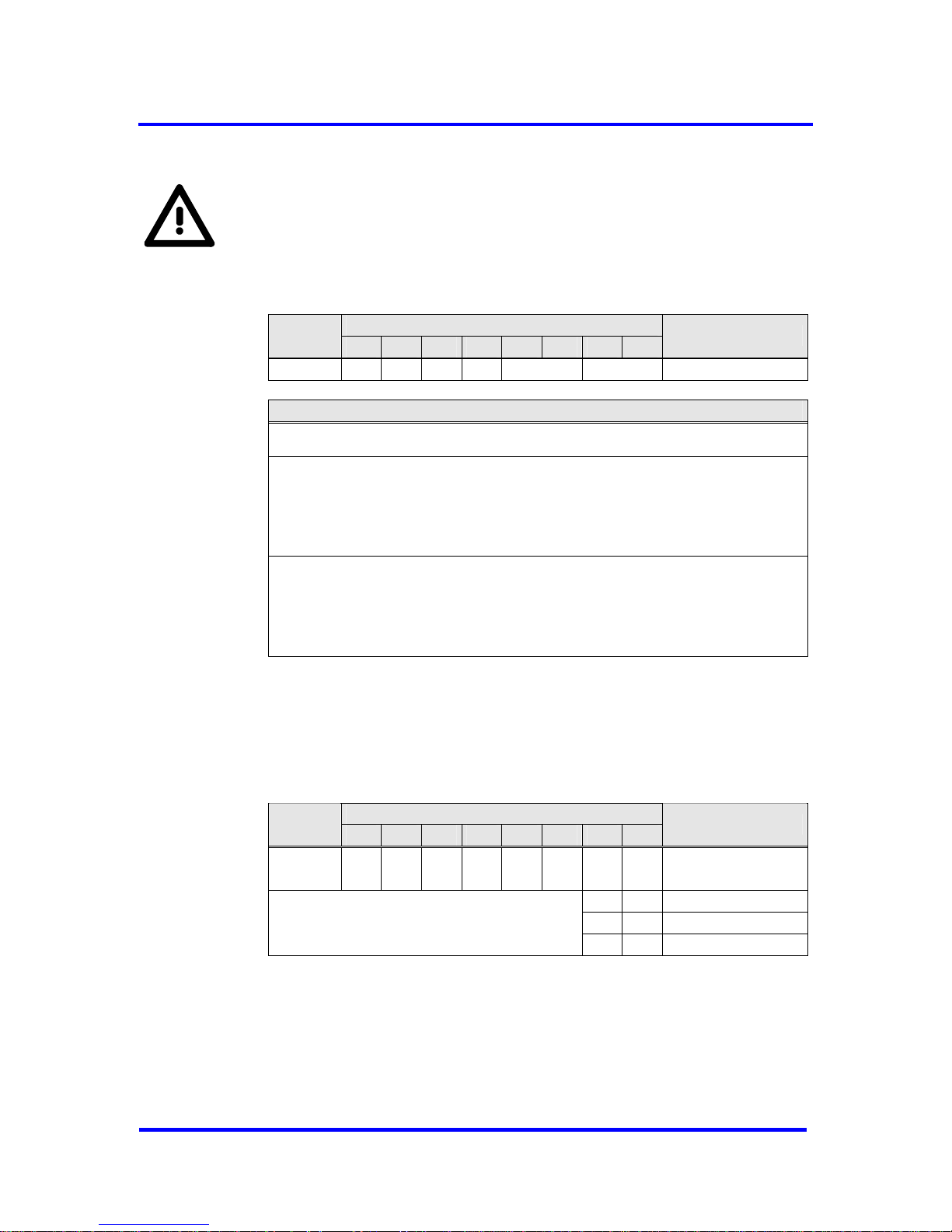
Status coding for the diagnosis buffers is stored in the Diag_Buffer_SM
control parameter. The user can read this cell with th
b
Bit Position
Address
7 6 5 4 3 2 1 0
Designation
0CH 0 0 0 0 Diag_Buf2 Diag_Buf1 Diag_Buffer_SM
Diag_Buffer_SM, Address 0CH:
bit 7-4
Don’t care: Read as ‘0’
bit 3-2
f2: Assignment of Diagnosis Buffer 2
11 = VPC3_Send_Mode
Diag_Bu
00 = Nil
01 = User
10 = VPC3+
bit 1-0
f1: Assignment of Diagnosis Buffer 1
11 = VPC3_Send_Mode
Diag_Bu
00 = Nil
01 = User
10 = VPC3+
Figure 6-9: Diagnosis Buffer Assignment
e currently assigned to the VPC3+C (No_Buffer,
iag_Buf1, Diag_Buf2).
The New_Diag_Cmd is also a read access to a defined control parameter
indicating which Diagnosis-Buffer belongs to the user after the exchange or
whether both buffers ar
D
Bit Position
Address
7 6 5 4 3 2 1 0
Designation
0DH 0 0 0 0 0 0
⇓ ⇓
New_Diag_
Buffer_Cmd
0 0 No_Buffer
0 1 Diag_Buf1
1 0 Diag_Buf2
Figure 6-10: Coding of New_Diag_Cmd
VPC3+C User Manual
Revision 1.03 45
Copyright © profichip GmbH 2004-2006
Page 46
6 PROFIBUS DP Interface
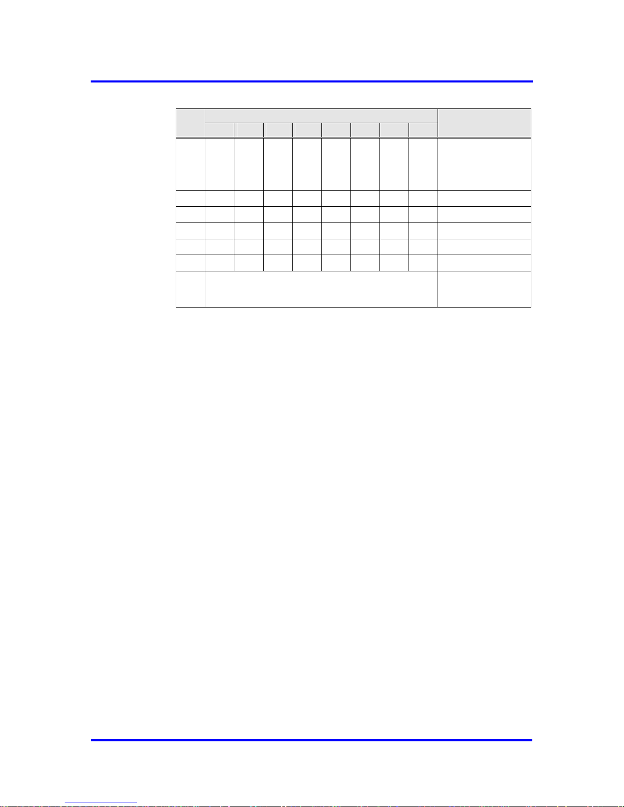
Bit Position
Byte
7 6 5 4 3 2 1 0
Designation
0
Ext_Diag_
Overflow
Stat_Diag
Ext_Diag
1
2
3
4
5
6
:
n
user input
Ext_Diag_Data
(n = max. 243)
Figure 6-11: Format of the Diagnosis-Buffer
The Ext_Diag_Data must be entered into the buffers after the VPC3+C
internal diagnosis data. Three different formats are possible here: devicerelated, ID-related and port-related. If PROFIBUS DP extensions shall be
used, the device-related diagnosis is substituted by alarm and status
messages. In addition to the Ext_Diag_Data, the buffer length also includes
the VPC3+C diagnosis bytes (R_Len_Diag_Buf 1, R_Len_Diag_Buf 2).
6.2.5 Write_Read_Data / Data_Exchange (Default_SAP)
Writing Outputs
The VPC3+C writes the received output data in the 'D' buffer. After an
error-free receipt, the VPC3+C shifts the newly filled buffer from ‘D’ to ‘N'.
In addition, the DX_Out interrupt is generated. The user now fetches the
current output data from ‘N’. The buffer changes from ‘N’ to ‘U’ with the
Next_Dout_Buffer_Cmd, so that the current data can be transmitted to the
application by a RD_Output request from a DP-Master.
If the user’s evaluation cycle time is shorter than the bus cycle time, the
user does not find any new buffers with the next Next_Dout_Buffer_Cmd in
‘N'. Therefore, the buffer exchange is omitted. At a 12 Mbit/s baud rate, it is
more likely, however, that the user’s evaluation cycle time is larger than the
bus cycle time. This makes new output data available in ‘N’ several times
before the user fetches the next buffer. It is guaranteed, however, that the
user receives the data last received.
For power-on, LEAVE-MASTER and the Global_Control telegram with
‘Clear_Data = 1’, the VPC3+C deletes the ‘D’ buffer and then shifts it to ‘N'.
This also takes place during power-up (entering the WAIT-PRM state). If
the user fetches this buffer, he receives U_Buffer_Cleared during the
46 Revision 1.03
VPC3+C
User Manual
Copyright © profichip GmbH 2004-2006
Page 47
PROFIBUS DP Interface 6
Next_Dout_Buffer_Cmd. If the user is supposed to enlarge the output data
buffer after the Chk_Cfg telegram, the user must delete this deviation in the
'N' buffer himself (possible only during the start-up phase in the WAIT-CFG
state).
If ‘Diag.Sync_Mode = 1’, the ‘D’ buffer is filled but not exchanged with the
Data_Exchange telegram. It is exchanged at the next Sync or Unsync
command sent by Global_Control telegram.
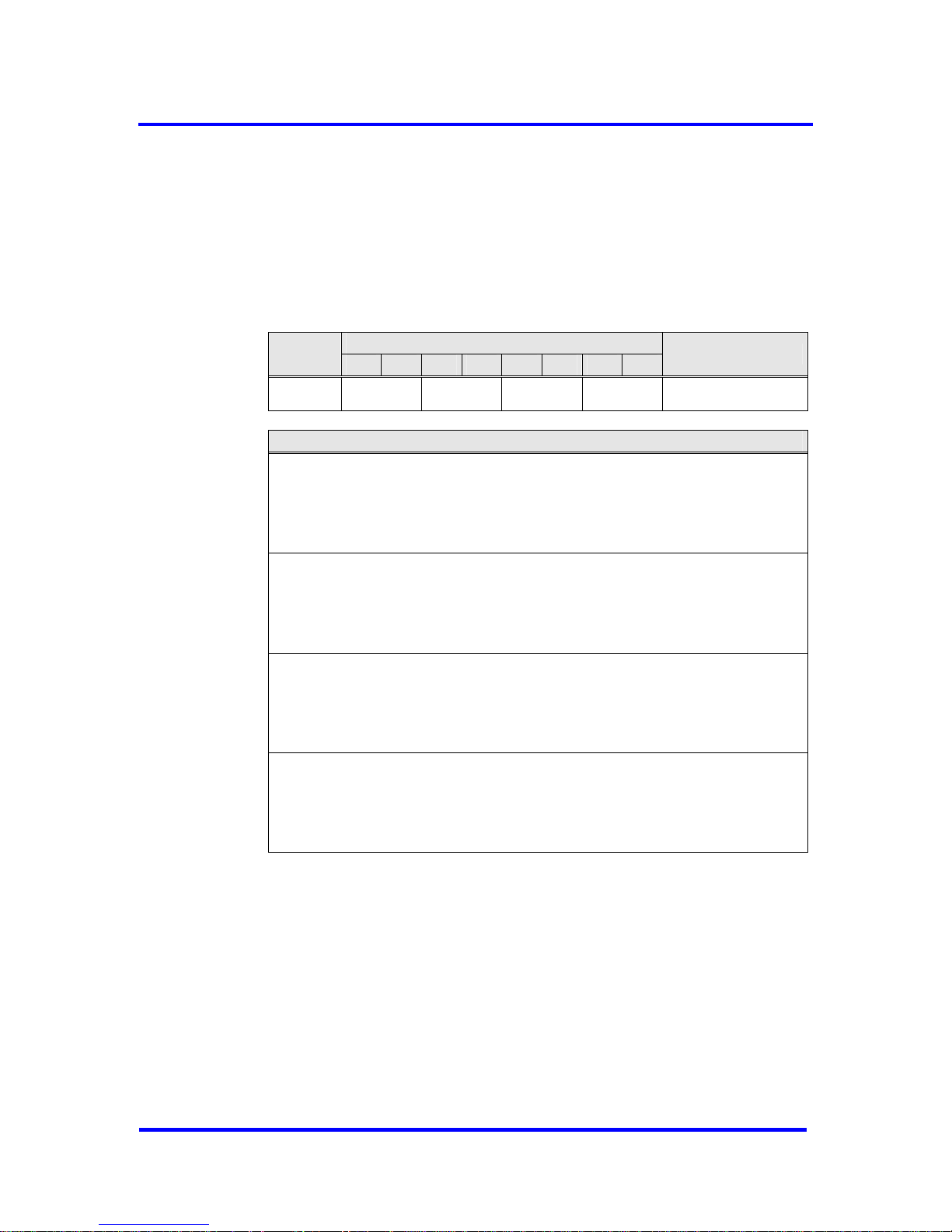
Bit Position
Address
7 6 5 4 3 2 1 0
Designation
0AH F U N D Dout_Buffer_SM
Dout_Buffer_SM, Address 0AH:
bit 7-6
F: Assignment of the F-Buffer
00 = Nil
01 = Dout_Buf_Ptr1
10 = Dout_Buf_Ptr2
11 = Dout_Buf_Ptr3
bit 5-4
U: Assignment of the U-Buffer
00 = Nil
01 = Dout_Buf_Ptr1
10 = Dout_Buf_Ptr2
11 = Dout_Buf_Ptr3
bit 3-2
N: Assignment of the N-Buffer
00 = Nil
01 = Dout_Buf_Ptr1
10 = Dout_Buf_Ptr2
11 = Dout_Buf_Ptr3
bit 1-0
D: Assignment of the D-Buffer
00 = Nil
01 = Dout_Buf_Ptr1
10 = Dout_Buf_Ptr2
11 = Dout_Buf_Ptr3
Figure 6-12: Dout-Buffer Management
When reading the Next_Dout_Buffer_Cmd the user gets the information
which buffer (‘U’ buffer) belongs to the user after the change, or whether a
change has taken place at all.
VPC3+C User Manual
Revision 1.03 47
Copyright © profichip GmbH 2004-2006
Page 48
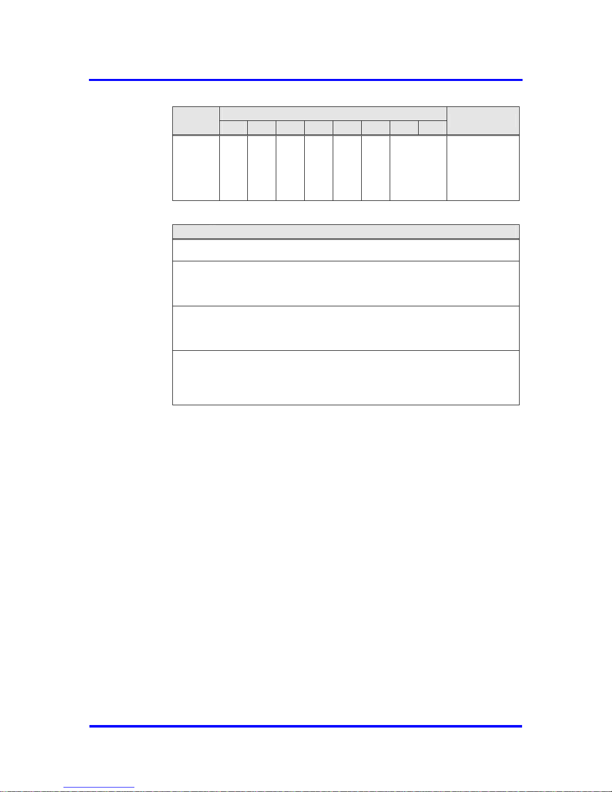
6 PROFIBUS DP Interface
Bit Position
Address
7 6 5 4 3 2 1 0
Designation
0BH 0 0 0 0
U_Buffer_
Cleared
State_U_
Buffer
Ind_U_
Buffer
Next_Dout_
Buf_Cmd
See coding
below
Next_Dout_Buf_Cmd, Address 0BH:
bit 7-4
Don’t care: Read as ‘0’
bit 3
U_Buffer_Cleared: User-Buffer-Cleared Flag
0 = U buffer contains data
1 = U buffer is cleared
bit 2
State_U_Buffer: State of the User-Buffer
0 = no new U buffer
1 = new U buffer
bit 1-0
Ind_U_Buffer: Indicated User-Buffer
01 = Dout_Buf_Ptr1
10 = Dout_Buf_Ptr2
11 = Dout_Buf_Ptr3
Figure 6-13: Coding of Next_Dout_Buf_Cmd
The user must clear the ‘U’ buffer during initialization so that defined
(cleared) data can be sent for a RD_Output telegram before the first data
cycle.
Reading Inputs
The VPC3+C sends the input data from the ‘D’ buffer. Prior to sending, the
VPC3+C fetches the Din-Buffer from ‘N’ to ‘D'. If no new buffer is present in
‘N', there is no change.
The user makes the new data available in ‘U’. With the
New_Din_Buffer_Cmd, the buffer changes from ‘U’ to ‘N’. If the user’s
preparation cycle time is shorter than the bus cycle time, not all new input
data are sent, but just the most current. At a 12 Mbit/s baud rate, it is more
likely, however, that the user’s preparation cycle time is larger than the bus
cycle time. Then the VPC3+C sends the same data several times in
succession.
During start-up, the VPC3+C does not go to DATA-EXCH before all
parameter telegrams and configuration telegrams have been
acknowledged.
48 Revision 1.03
VPC3+C
User Manual
Copyright © profichip GmbH 2004-2006
Page 49
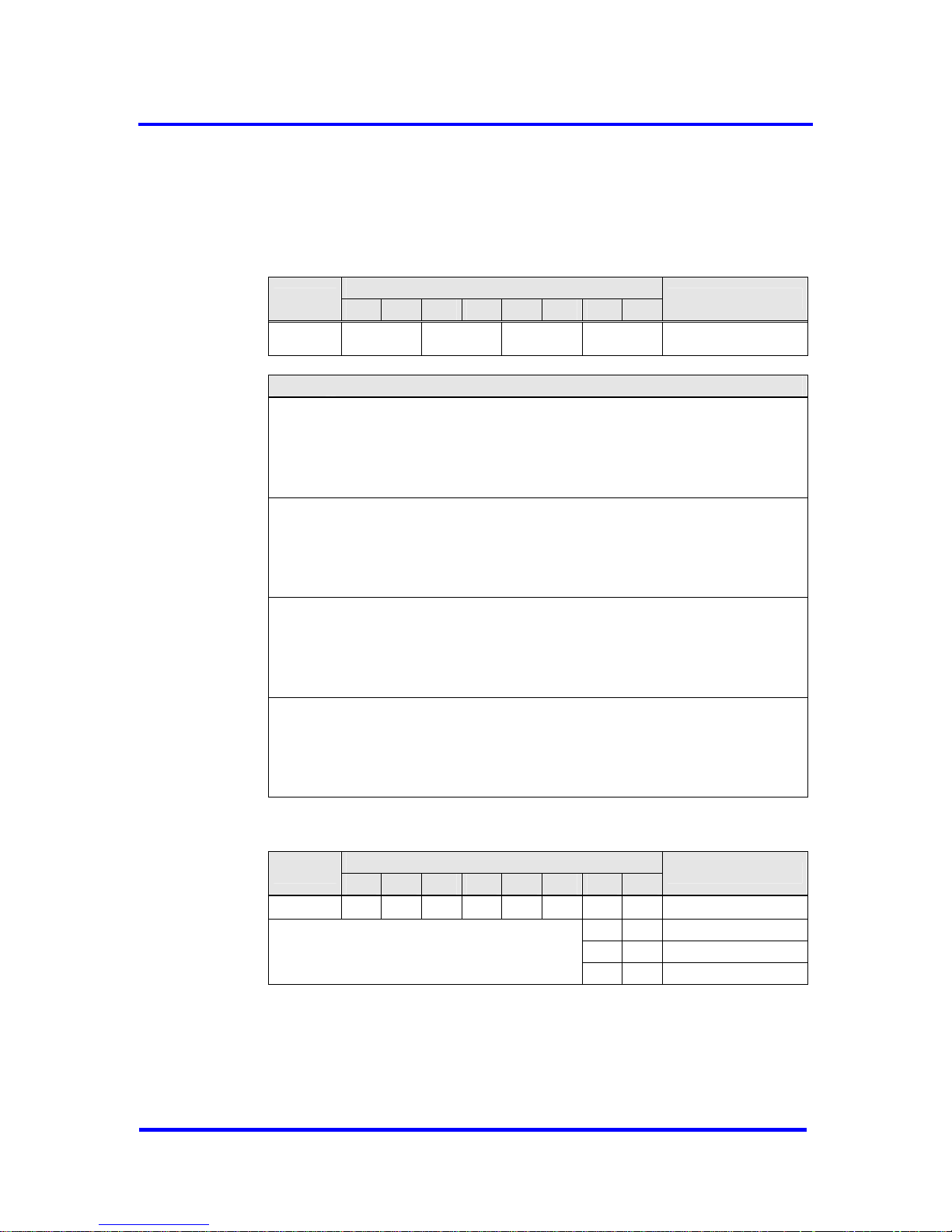
PROFIBUS DP Interface 6
If ‘Diag.Freeze_Mode = 1’, there is no buffer change prior to sending.
The user can read the status of the state machine cell with the following
codings for the four states: Nil, Dout_Buf_Ptr1, Dout_Buf_Ptr2 and
Dout_Buf_Ptr3. The pointer for the current data is in the 'N' state.
Bit Position
Address
7 6 5 4 3 2 1 0
Designation
08H F U N D Din_Buffer_SM
Din_Buffer_SM, Address 08H:
bit 7-6
F: Assignment of the F-Buffer
00 = Nil
01 = Din_Buf_Ptr1
10 = Din_Buf_Ptr2
11 = Din_Buf_Ptr3
bit 5-4
U: Assignment of the U-Buffer
00 = Nil
01 = Din_Buf_Ptr1
10 = Din_Buf_Ptr2
11 = Din_Buf_Ptr3
bit 3-2
N: Assignment of the N-Buffer
00 = Nil
01 = Din_Buf_Ptr1
10 = Din_Buf_Ptr2
11 = Din_Buf_Ptr3
bit 1-0
D: Assignment of the D-Buffer
00 = Nil
01 = Din_Buf_Ptr1
10 = Din_Buf_Ptr2
11 = Din_Buf_Ptr3
Figure 6-14: Din-Buffer Management
Bit Position
Address
7 6 5 4 3 2 1 0
Designation
09H 0 0 0 0 0 0
⇓ ⇓
New_Din_Buf_Cmd
0 1 Din_Buf_Ptr1
1 0 Din_Buf_Ptr2
1 1 Din_Buf_Ptr3
Figure 6-15: Coding of New_Din_Buf_Cmd
VPC3+C User Manual
Revision 1.03 49
Copyright © profichip GmbH 2004-2006
Page 50

6 PROFIBUS DP Interface
User_Watchdog_Timer
After start-up (DATA-EXCH state), it is possible that the VPC3+C continually answers Data_Exchange telegrams without the user fetching the received Dout-Buffers or making new Din-Buffers available. If the user processor ‘hangs up' the DP-Master would not receive this information. Therefore, a User_Watchdog_Timer is implemented in the VPC3+C.
This User_WD_Timer is an internal 16-bit RAM cell that is started from a
user parameterized value R_User_WD_Value and is decremented by the
VPC3+C with each received Data_Exchange telegram. If the timer reaches
the value 0000H, the VPC3+C goes to the WAIT-PRM state and the
DP_SM carries out a LEAVE-MASTER. The user must cyclically set this
timer to its start value. Therefore, ‘Res_User_WD = 1’ must be set in Mode
Register 1. Upon receipt of the next Data_Exchange telegram, the VPC3+C
again loads the User_WD_Timer to the parameterized value
R_User_WD_Value and sets ‘Res_User_WD = 0’ (Mode Register 1). During power-up, the user must also set ‘Res_User_WD = 1’, so that the
User_WD_Timer is set to its parameterized value.
6.2.6 Global_Control (SAP 58)
The VPC3+C processes the Global_Control telegrams like already
described.
The first byte of a valid Global_Control is stored in the R_GC_Command
RAM cell. The second telegram byte (Group_Select) is processed
internally.
The interrupt behavior regarding to the reception of a Global_Control
telegram can be configured via bit 8 of Mode Register 2. The VPC3+C
either generates the New_GC_Control interrupt after each receipt of a
Global_Control telegram (default) or just in case if the Global_Control
differs from the previous one.
The R_GC_Command RAM cell is not initialized by the VPC3+C. Therefore
the cell has to be preset with 00H during power-up. The user can read and
evaluate this cell.
In order to use Sync and Freeze, these functions must be enabled in the
Mode Register 0.
50 Revision 1.03
VPC3+C
User Manual
Copyright © profichip GmbH 2004-2006
Page 51
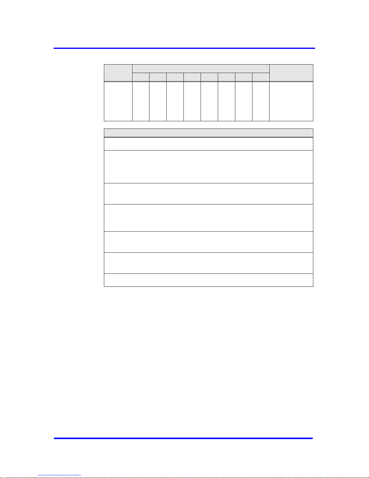
PROFIBUS DP Interface 6
Bit Position
Address
7 6 5 4 3 2 1 0
Designation
3CH
Reserved
Reserved
Sync
Unsync
Freeze
Unfreeze
Clear_Data
Reserved
R_GC_
Command
See below
for coding
R_GC_Command, Address 3CH:
bit 7-6
Reserved
bit 5
Sync:
The output data transferred with a Data_Exchange telegram is changed from ‘D’
to ‘N’. The following transferred output data is kept in ‘D’ until the next Sync
command is given.
bit 4
Unsync:
The Unsync command cancels the Sync command.
bit 3
Freeze:
The input data is fetched from ‘N’ to ‘D’ and „frozen“. New input data is not
fetched again until the DP-Master sends the next Freeze command.
bit 2
Unfreeze:
The Unfreeze command cancels the Freeze command.
bit 1
Clear_Data:
With this command, the output data is deleted in ‘D’ and is changed to ‘N’.
bit 0
Reserved
Figure 6-16: Format of the Global_Control Telegram
6.2.7 RD_Input (SAP 56)
The VPC3+C fetches the input data like it does for the Data_Exchange
telegram. Prior to sending, ‘N’ is shifted to ‘D', if new input data are
available in ‘N'. For ‘Diag.Freeze_Mode = 1', there is no buffer change.
6.2.8 RD_Output (SAP 57)
The VPC3+C fetches the output data from the Dout_Buffer in ‘U’. The user
must preset the output data with ‘0’ during start-up so that no invalid data
can be sent here. If there is a buffer change from ‘N’ to ‘U’ (through the
Next_Dout_Buffer_Cmd) between the first call-up and the repetition, the
new output data is sent during the repetition.
VPC3+C User Manual
Revision 1.03 51
Copyright © profichip GmbH 2004-2006
Page 52

6 PROFIBUS DP Interface
6.2.9 Get_Cfg (SAP 59)
The user makes the configuration data available in the Read_Config-Buffer.
For a change in the configuration after the Chk_Cfg telegram, the user
writes the changed data in the Config-Buffer, sets
‘En_Change_Cfg_buffer = 1’ (see Mode Register 1) and the VPC3+C then
exchanges the Config-Buffer for the Read_Config-Buffer. If there is a
change in the configuration data during operation (for example, for a
modular DP systems), the user must return with Go_Offline command (see
Mode Register 1) to WAIT-PRM.
52 Revision 1.03
VPC3+C
User Manual
Copyright © profichip GmbH 2004-2006
Page 53
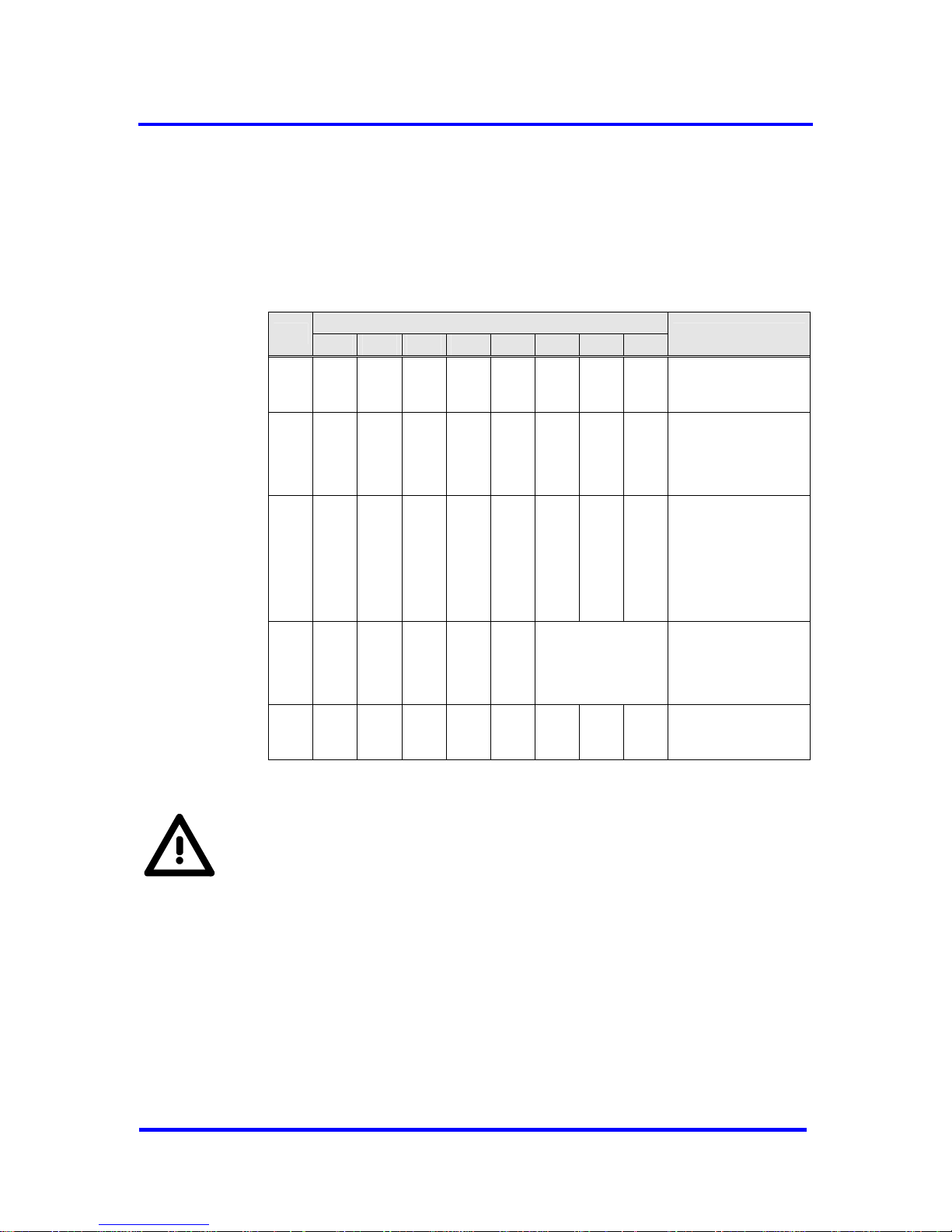
PROFIBUS DP Extensions 7
7 PROFIBUS DP Extensions
7.1 Set_(Ext_)Prm (SAP 53 / SAP 61)
The PROFIBUS DP extensions require three bytes to implement the new
parameterization function. The bits of the Spec_User_Prm_Byte are
included.
Bit Position
Byte
7 6 5 4 3 2 1 0
Designation
0
: 6
7
DPV1_
Enable
Fail_Safe
Publisher_
Enable
Reserved
Reserved
WD_Base
Dis_Stop_
Control
Dis_Start_
Control
DPV1_Status_1
8
Enable_
Pull_Plug_Alarm
Enable_
Process_Alarm
Enable_
Diagnostic_Alarm
Enable
_
Manufacturer_
S
p
ecific Alarm
Enable_
Status_Alarm
Enable_
Update_Alarm
0
Chk_Cfg_Mode
DPV1_Status_2
9
PrmCmd
0 0
IsoM_Req
Prm_
Structure
Alarm_Mode DPV1_Status_3
10
:
243
User_Prm_Data
Figure 7-1: Set_Prm with DPV1_Status bytes
If the extensions are used, the bit Spec_Clear_Mode in Mode
Register 0 serves as Fail_Safe_required. Therefore it is used for a
comparison with the bit Fail_Safe in parameter telegram. Whether the
DP-Master support the Fail_Safe mode or not is indicated by the
telegram bit. If the DP-Slave requires Fail_Safe but the DP-Master
doesn’t the Prm_Fault bit is set.
If the VPC3+C should be used for DXB, IsoM or redundancy mode, the
parameterization data must be packed in a Structured_Prm_Data block to
distinguish between the User_Prm_Data. The bit Prm_Structure indicates
this.
If redundancy should be supported, the PrmCmd_Supported bit in Mode
Register 0 must be set.
VPC3+C User Manual
Revision 1.03 53
Copyright © profichip GmbH 2004-2006
Page 54
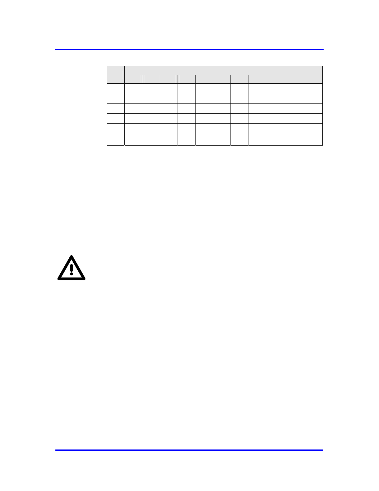
7 PROFIBUS DP Extensions
Bit Position
Byte
7 6 5 4 3 2 1 0
Designation
0
Structured_Length
1 Structure_Typ
2 Slot_Number
3 Reserved
4
:
243
User_Prm_Data
Figure 7-2 : Format of the Structured_Prm_Data block
Additional to the Set_Prm telegram (SAP 61) a Set_Ext_Prm (SAP 53)
telegram can be used for parameterization. This service is only available in
state WAIT-CFG after the reception of a Set_Prm telegram and before the
reception of a Chk_Cfg telegram. The new Set_Ext_Prm telegram simply
consists of Structured_Prm_Data blocks.
The new service uses the same buffer handling as described by Set_Prm.
By means of the New_Ext_Prm_Data interrupt the user can recognize
which kind of telegram is entered in the Parameter-Buffer. Additional the
SAP 53 must be activated by Set_Ext_Prm_Supported bit in Mode Register
0.
The Aux-Buffer for the Set_Ext_Prm is the same as the one for
Set_Prm and have to be different from the Chk_Cfg Aux-Buffer.
Furthermore the Spec_Prm_Buf_Mode in Mode Register 0 must not be
used together with SAP 53.
7.2 PROFIBUS DP-V1
7.2.1 Acyclic Communication Relationships
The VPC3+C supports acyclic communication as described in the DP-V1
specification. Therefore a memory area is required which contains all SAPs
needed for the communication. The user must do the initialization of this
area (SAP-List) in Offline state. Each entry in the SAP-List consists of 7
bytes. The pointer at address 17H contains the segment base address of
the first element of the SAP-List. The last element in the list is always
indicated with FFH. If the SAP-List shall not be used, the first entry must be
FFH, so the pointer at address 17H must point to a segment base address
location that contains FFH.
The new communication features are enabled with DPV1_Enable in the
Set_Prm telegram.
54 Revision 1.03
VPC3+C
User Manual
Copyright © profichip GmbH 2004-2006
Page 55
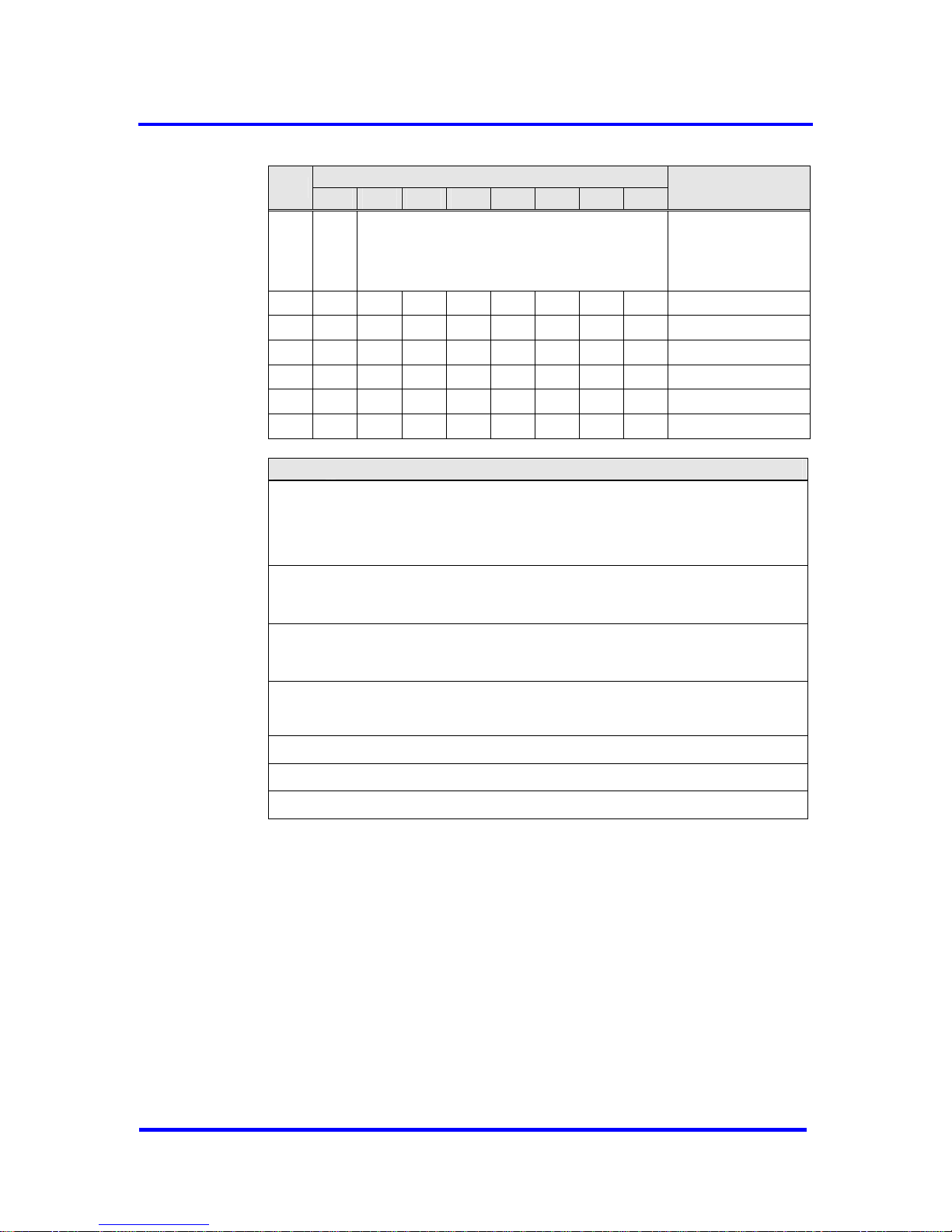
PROFIBUS DP Extensions 7
Bit Position
Byte
7 6 5 4 3 2 1 0
Designation
0
Response
_Sent
SAP_Number SAP_Number
1 Request_SA
2 Request_SSAP
3 Service_Supported
4 Ind_Buf_Ptr[0]
5 Ind_Buf_Ptr[1]
6 Resp_Buf_Ptr
SAP-List entry:
Byte 0
Response_Sent: Response-Buffer sent
0 = no Response sent
1 = Response sent
SAP_Number: 0 – 51
Byte 1
Request_SA: The source address of a request is compared with this value. At
differences, the VPC3+C response with “no service activated” (RS). The default
value for this entry is 7FH.
Byte 2
Request_SSAP: The source SAP of a request is compared with this value. At
differences, the VPC3+C response with “no service activated” (RS). The default
value for this entry is 7FH.
Byte 3
Service_Supported: Indicates the permitted FDL service.
00 = all FDL services allowed
Byte 4
Ind_Buf_Ptr[0]: pointer to Indication-Buffer 0
Byte 5
Ind_Buf_Ptr[1]: pointer to Indication-Buffer 1
Byte 6
Resp_Buf_Ptr: pointer to Response-Buffer
Figure 7-3: SAP-List entry
In addition an Indication- and Response-Buffer are needed. Each buffer
consists of a 4-byte header for the buffer management and a data block of
configurable length.
VPC3+C User Manual
Revision 1.03 55
Copyright © profichip GmbH 2004-2006
Page 56
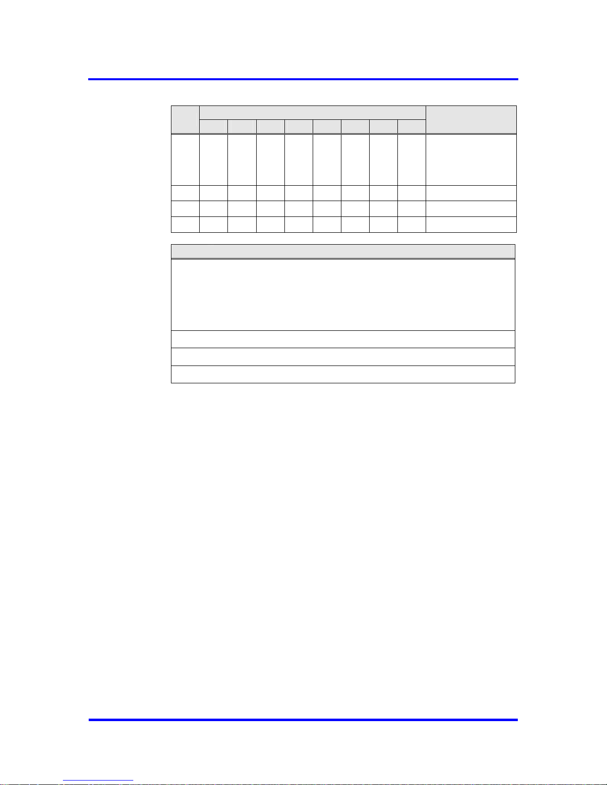
7 PROFIBUS DP Extensions
Bit Position
Byte
7 6 5 4 3 2 1 0
Designation
0
USER
IND
RESP
INUSE
Control
1 Max_Length
2 Length
3 Function Code
SAP-List entry:
Byte 0
Control: bits for buffer management
USER buffer assigned to user
IND indication data included in buffer
RESP response data included in buffer
INUSE buffer assigned to VPC3+C
Byte 1
Max_Length: length of buffer
Byte 2
Length: length of data included in buffer
Byte 3
Function Code: function code of the telegram
Figure 7-4: Buffer Header
Processing Sequence
A received telegram is compared with the values in the SAP-List. If this
check is positive, the telegram is stored in an Indication-Buffer with the
INUSE bit set. In case of any deviations the VPC3+C responses with “no
service activated” (RS) or if no free buffer is available with “no resource”
(RR). After finishing the processing of the incoming telegram, the INUSE bit
is reset and the bits USER and IND are set by VPC3+C. Now the FDL_Ind
interrupt is generated. Polling telegrams do not produce interrupts. The
RESP bit indicates response data, provided by the user in the ResponseBuffer. The Poll_End_Ind interrupt is set after the Response-Buffer is sent.
Also bits RESP and USER are cleared.
56 Revision 1.03
VPC3+C
User Manual
Copyright © profichip GmbH 2004-2006
Page 57

PROFIBUS DP Extensions 7
DP-Master PROFIBUS DP-Slave
Request to acyclic SAP ->
fill
Indication-Buffer
<- short acknowledgement (SC)
Polling telegram to acyclic SAP ->
<- short acknowledgement (SC)
:
:
process data
:
update Response-
Buffer
Polling telegram to acyclic SAP ->
<- Response from acyclic
Figure 7-5: acyclic communication sequence
VPC3+C Firmware
set Request_SA / Request_SSA
set INUSE in Control of Ind_Buf
write data in Ind_Buf
clear INUSE and set USER and IND in Control of Ind_Buf
set FDL_Ind interrupt
clear FDL_Ind interrupt
search for Ind_Buf with IND = 1
read Ind_Buf
clear IND in Control of Ind_Buf
write Response in Resp_Buf
set RESP in Control of Resp_Buf
check on RESP = 1
read Resp_Buf
clear RESP and USER in Control of Resp_Buf
set Response_Sent
set Poll_End_Ind interrupt
clear Poll_End_Ind interrupt
search for SAP with Response_Sent = 1
clear Response_Sent
Figure 7-6: FDL-Interface of VPC3+C (e.g. same Buffer for Indication and Response)
7.2.2 Diagnosis Model
The format of the device related diagnosis data depends on the GSD
keyword DPV1_Slave in the GSD. If 'DPV1_Slave = 1', alarm and status
messages are used in diagnosis telegrams. Status messages are required
by the Data eXchange Broadcast service, for example. Alarm_Ack is used
as the other acyclic services.
VPC3+C User Manual
Revision 1.03 57
Copyright © profichip GmbH 2004-2006
Page 58
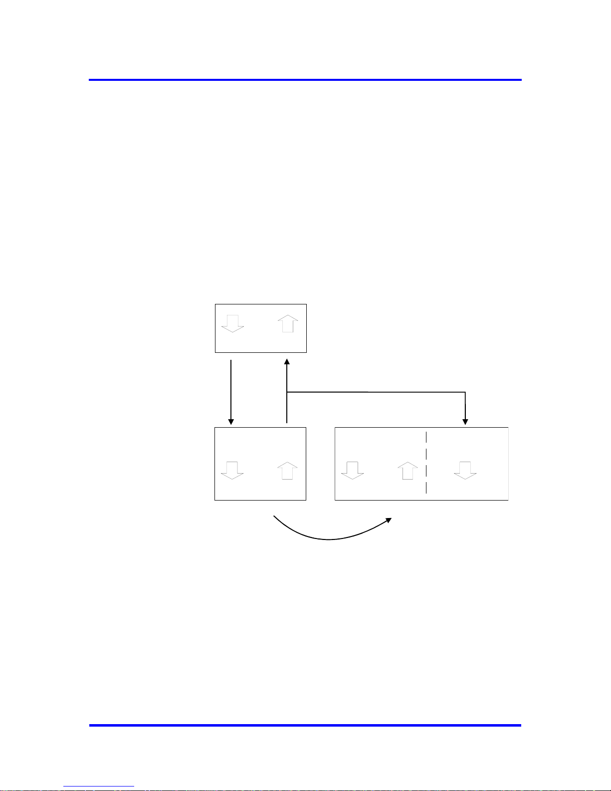
7 PROFIBUS DP Extensions
7.3 PROFIBUS DP-V2
7.3.1 DXB (Data eXchange Broadcast)
The DXB mechanism enables a fast slave-to-slave communication. A DPSlave that holds input data significant for other DP-Slaves, works as a
Publisher. The Publisher can handle a special kind of Data_Exchange
request from the DP-Master and sends its answer as a broadcast telegram.
Other DP-Slaves that are parameterized as Subscribers can monitor this
telegram. A link is opened to the Publisher if the address of the Publisher is
registered in the linktable of the Subscriber. If the link have been
established correctly, the Subscriber can fetch the input data from the
Publisher.
Dout Din DXBout
DP-Slave (Subscriber)
Data Exchange with
DP-Master (Class 1)
filtered
Broadcast (Input) Data
from Publisher
Dout Din
DP-Slave (Publisher)
Data Exchange with
DP-Master (Class 1)
Dout Din
DP-Master (Class1)
Link
Figure 7-7 : Overview DXB
he VPC3+
Response (DA=127)
C can handle a maximum of 29 links simultaneously.
Publisher
A Publisher is activated with 'Publisher_Enable = 1' in DPV1_Status_1. The
time minT
SDR
must be set to 'T
ID1
= 37 t
bit
+ 2 T
SET
+ T
QUI
'.
All Data_Exchange telegrams containing the function code 7 (Send and
Request Data Multicast) are responded with destination address 127. If
Publisher mode is not enabled, these requests are ignored.
Request (FC=7)
T
58 Revision 1.03
VPC3+C
User Manual
Copyright © profichip GmbH 2004-2006
Page 59
PROFIBUS DP Extensions 7
Subscriber
A Subscriber requires infor atio bou he ks to its Publishers. These
settings are contained in a DXB Linktable or DXB Subscribertable and
transferred via the Structured_Prm_Data in a Set_Prm o Prm
te ram ac tru red rm_ ta trea d lik th Data
and therefore evaluated by the user. From the received data the user must
ge rate XB_ ink_ f an DXB Stat _Bu ntri . T dog must
be enabled to make use of the must
check th
m n a t t lin
r Set_Ext_
e User_Prm_leg . E h S ctu _P Da is te e
ne D L Bu d _ us f e es he watch
monitoring mechanism. The user
is.
Bit Position
B yte
7 6 5 4 3 2 1 0
Designation
0
h Structured_Lengt
1 0 0 0 0 0 0 1 1 Structure_Type
2 0 0 0 0 0 0 0 0 Slot_Number
3 0 0 0 0 0 0 0 0 Reserved
4 0 0 0 0 0 0 0 1 Version
5 Publisher_Addr
6 Publisher_Length
7 Sample_Offset
8 Sample_Length
9
:
120
further link entries
Figure 7-8 orm f th truc ed_P _Da ith DXB Li tab
ecific link is grey caled
: F at o e S tur rm ta w nk le
(sp s )
VPC3+C User Manual
Revision 1.03 59
Copyright © profichip GmbH 2004-2006
Page 60
7 PROFIBUS DP Extensions
Bit Position
Byte
7 6 5 4 3 2 1 0
Designation
0
Structured_Length
1 0 0 0 0 0 1 1 1 Structure_Type
2 0 0 0 0 0 0 0 0 Slot_Number
3 0 0 0 0 0 0 0 0 Reserved
4 0 0 0 0 0 0 0 1 Version
5 Publisher_Addr
6 Publisher_Length
7 Sample_Offset
8 Dest_Slot_Number
9 Offset_Data_Area
10 Sample_Length
11
:
120
further link entries
Figure 7-9: Format of the Structured_Prm_Data with DXB Subscribertable
(specific link is grey scaled)
The user must copy the link entries of DXB Linktable or DXB
Subscribertable, without Dest_Slot_Number and Offset_Data_Area, in the
DXB_Link_Buf and set R_Len_DXB_Link_Buf. Also the user must enter the
default status message in DXB_Status_Buf with the received links and
write the appropriate values to R_Len_DXB_Status_Buf. After that, the
parameterization interrupt can be acknowledged.
60 Revision 1.03
VPC3+C
User Manual
Copyright © profichip GmbH 2004-2006
Page 61
PROFIBUS DP Extensions 7
Bit Position
Byte
7 6 5 4 3 2 1 0
Designation
0 0 0 Block_Length Header_Byte
1 1 0 0 0 0 0 1 1 Status_Type
2 0 0 0 0 0 0 0 0 Slot_Number
3 0 0 0 0 0 0 0 0 Status_Specifier
4 Publisher_Addr
5
Link_
Status
Link_
Error
0 0 0 0 0
Data_
Exist
Link_Status
6
:
61
further link entries
Link_Status:
bit 7
Link_Status :
1 = active, valid data receipt during last monitoring period
0 = not active, no valid data receipt during last monitoring period (DEFAULT)
bit 6
Link_Error:
0 = no faulty Broadcast data receipt (DEFAULT)
1 = wrong length, error occurred by reception
bit 0
Data_Exist:
0 = no correct Broadcast data receipt during current monitoring period
(DEFAULT)
1 = error free reception of Broadcast data during current monitoring period
Figure 7-10: DXB_Link_Status_Buf (specific link is grey scaled)
Processing Sequence
The VPC3+C processes DXBout-Buffers like the Dout-Buffers. The only
difference is that the DXBout-Buffers are not cleared by the VPC3+C.
The VPC3+C writes the received and filtered broadcast data in the 'D'
buffer. The buffer contains also the Publisher_Address and the
Sample_Length. After error-free receipt, the VPC3+C shifts the newly filled
buffer from 'D' to 'N'. In addition, the DXBout interrupt is generated. The
user now fetches the current output data from 'N'. The buffer changes from
'N' to 'U' with the Next_DXBout_Buffer_Cmd.
VPC3+C User Manual
Revision 1.03 61
Copyright © profichip GmbH 2004-2006
Page 62
7 PROFIBUS DP Extensions
Bit Position
Byte
7 6 5 4 3 2 1 0
Designation
0 Publisher_Addr
1 Sample_Length
2
:
246
Sample_Data
Figure 7-11: DXBout-Buffer
When reading the Next_DXBout_buffer_Cmd the user gets the information
which buffer ('U' buffer) is assigned to the user after the change, or whether
a change has taken place at all.
Bit Position
Address
7 6 5 4 3 2 1 0
Designation
12H F U N D DXBout_Buffer_SM
DXBout_Buffer_SM, Address 12H:
bit 7-6
F: Assignment of the F-Buffer
00 = Nil
01 = DXBout_Buf_Ptr1
10 = DXBout_Buf_Ptr2
11 = DXBout_Buf_Ptr3
bit 5-4
U: Assignment of the U-Buffer
00 = Nil
01 = DXBout_Buf_Ptr1
10 = DXBout_Buf_Ptr2
11 = DXBout_Buf_Ptr3
bit 3-2
N: Assignment of the N-Buffer
00 = Nil
01 = DXBout_Buf_Ptr1
10 = DXBout_Buf_Ptr2
11 = DXBout_Buf_Ptr3
bit 1-0
D: Assignment of the D-Buffer
00 = Nil
01 = DXBout_Buf_Ptr1
10 = DXBout_Buf_Ptr2
11 = DXBout_Buf_Ptr3
Figure 7-12: DXBout-Buffer Management
62 Revision 1.03
VPC3+C
User Manual
Copyright © profichip GmbH 2004-2006
Page 63
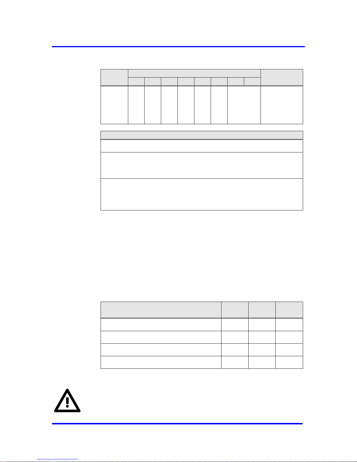
PROFIBUS DP Extensions 7
Bit Position
Address
7 6 5 4 3 2 1 0
Designation
13H 0 0 0 0 0
State_U_
Buffer
Ind_U_
Buffer
Next_DXBout_
Buf_Cmd
See coding
below
Next_DXBout_Buf_Cmd, Address 13H:
bit 7-3
Don’t care: Read as ‘0’
bit 2
State_U_Buffer: State of the User-Buffer
0 = no new U buffer
1 = new U buffer
bit 1-0
Ind_U_Buffer: Indicated User-Buffer
01 = DXBout_Buf_Ptr1
10 = DXBout_Buf_Ptr2
11 = DXBout_Buf_Ptr3
Figure 7-13: Coding of Next_DXBout_Buf_Cmd
Monitoring
After receiving the DXB data the Link_Status in DXB_Status_Buf of the
concerning Publisher is updated. In case of an error the bit Link_Error is
set. If the processing is finished without errors, the bit Data_Exist is set.
In state DATA-EXCH the links are monitored in intervals defined by the
parameterized watchdog time. After the monitoring time runs out, the
VPC3+C evaluates the Link_Status of each Publisher and updates the bit
Link_Status. The timer restarts again automatically.
Event
Link_
Status
Link_
Error
Data_
Exist
valid DXB data receipt 0 1
faulty DXB data receipt 0 1 0
WD_Time elapsed AND Data_Exist = 1 1 0 0
WD_Time elapsed AND Link_Error = 1 0 0 0
Figure 7-14: Link_Status handling
To enable the monitoring of Publisher-Subscriber links the watchdog
timer must be enabled in the Set_Prm telegram. The user must check
this.
VPC3+C User Manual
Revision 1.03 63
Copyright © profichip GmbH 2004-2006
Page 64
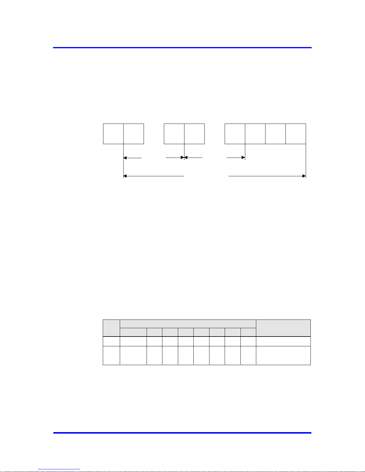
7 PROFIBUS DP Extensions
7.3.2 IsoM (Isochron Mode)
The IsoM synchronizes DP-Master, DP-Slave and DP-Cycle. The isochron
cycle time starts with the transmission of the SYNCH telegram by the IsoM
master. If the VPC3+C supports the IsoM, a synchronization signal at Pin
13 (XDATAEXCH/SYNC) is generated by each reception of a SYNCH
telegram. The SYNCH telegram is a special coded Global_Control request.
Cyclic
Service
Cyclic
Service
Acyclic
Service
Acyclic
Service
Token
Spare
Time
. . .
. . .
SYNCH
mesage
SYNCH
mesage
Cycle Time (TDP)
Cyclic
Part Part
Acyclic
gu lass 1)
Tw
VP
1.
2. auses a
DX_Out interrupt immediately, rather the event is stored in a flag. By a
following SYNCH message reception, the DX_Out interrupt and a
synchronization signa ated at the same time. Additionally a
w_G _Com and nte pt produced, as the SYNCH telegram
behaves like a regular Global_Control telegr
achin If D a_E chan e telegram p ce H
telegram, only the New_GC_Command interrupt is generated.
Fi re 7-15: Telegram sequences in IsoM with one DP-Master (C
o operation modes for cyclic synchronization are available in the
C3+C:
Isochron Mode: Each SYNCH telegram causes an impulse on the
SYNC output and a New_GC_Command interrupt.
Simple Sync Mode: A Data_Exchange telegram no longer c
l are gener
Ne C m i rru is
am to the DP state
m e. no at x g re des the SYNC
Bit Position
Byte
7 6 5 4 3 2 1 0
Designation
0 0 0 0 Control_Command
1
= 1
Group_Select
Group_8
Figure 7-16: IsoM SYNCH telegram
Each Global_Control is compared with the values that can be adjusted in
Control_Command_Reg (0Eh) and Group_Select_Reg (0Fh). If the values
are equal a SYNCH telegram will be detected.
64 Revision 1.03
VPC3+C
User Manual
Copyright © profichip GmbH 2004-2006
Page 65
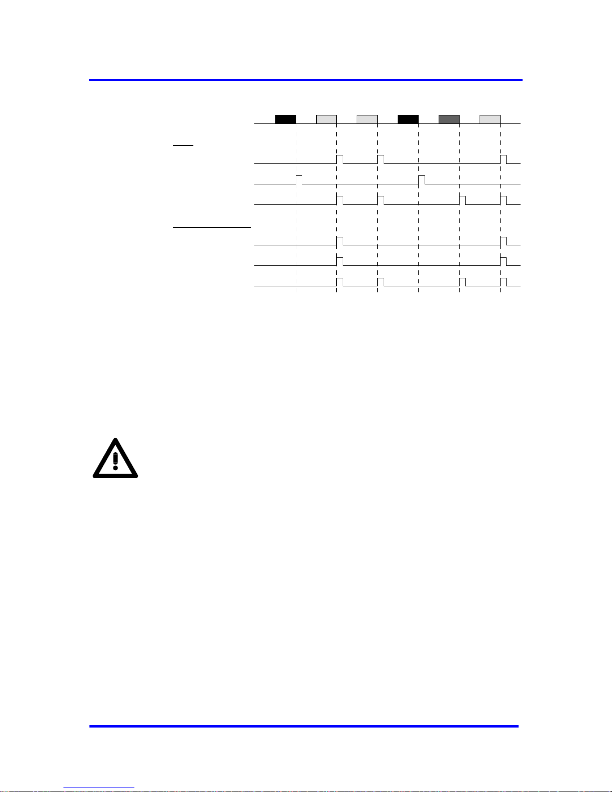
PROFIBUS DP Extensions 7
Data_Ex SYNCH SYNCH
Data_Ex
GC SYNCH
telegrams
SYNC
DX_Out*
New_GC_Command*
SYNC
DX_Out*
New_GC_Command*
IsoM
Simple Sync Mode
Figure 7-17: SYNC-signal and interrupts for synchronization modes (picture only
shows the effects by reception of telegrams; time between telegrams is not equal)
Isochron Mode
To enable the Isochron Mode in the VPC3+C, bit SYNC_Ena in Mode
Register 2 must be set. Additionally the Spec_Clear_Mode in Mode
Register 0 must be set. The polarity of the SYNC signal can be adjusted
with the SYNC_Pol bit. The register Sync_PW contains a multiplicator with
the base of 1/12 µs to adjust the SYNC pulse width. Settings in the
Set_Prm telegram are shown below.
The Structured_Prm_Data block IsoM (Structure_Type = 4) is also
required for the application. If it is sent by Set_Prm telegram the bit
Prm_Structure must be set.
VPC3+C User Manual
Revision 1.03 65
Copyright © profichip GmbH 2004-2006
Page 66

7 PROFIBUS DP Extensions
Bit Position
Byte
7 6 5 4 3 2 1 0
Designation
0
Sync_Req = 0
Freeze_Req = 0
Station_Status
1 WD_Fact_1
2 WD_Fact_2
3 minT
SDR
4 Ident_Number_High
5 Ident_Number_Low
6
Group_8 = 0
Group_Ident
7
Fail_Safe = 1
DPV1_Status_1
8 DPV1_Status_2
9
IsoM_Req = 1
DPV1_Status_3
10
:
246
User_Prm_Data
Figure 7-18: Format of Set_Prm telegram for IsoM
66 Revision 1.03
VPC3+C
User Manual
Copyright © profichip GmbH 2004-2006
Page 67
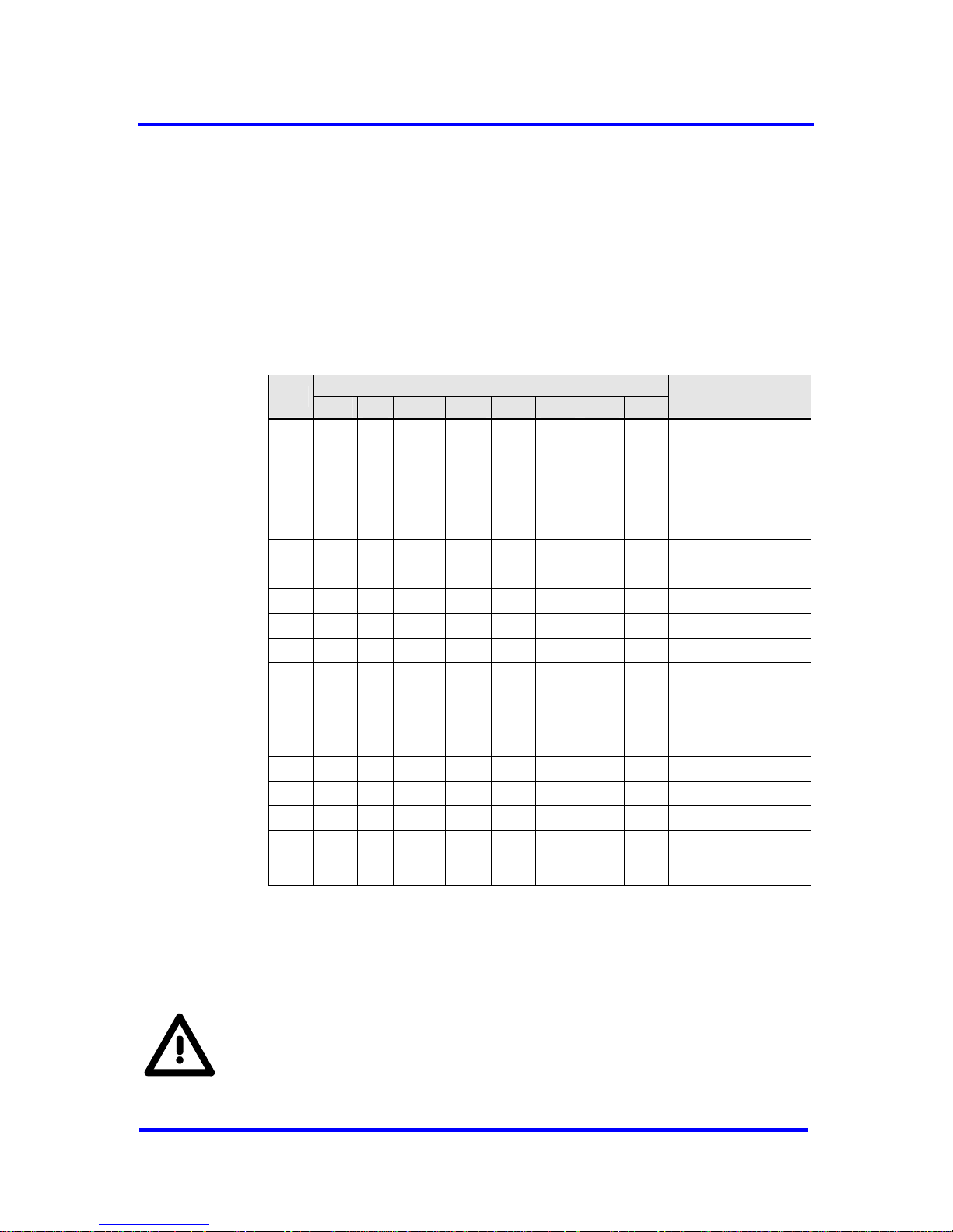
PROFIBUS DP Extensions 7
DP-Slave in a IsoM network
To enable cyclic synchronization via the ‘Simple Sync Mode', the bit
DX_Int_Port in Mode Register 2 have to be set. Bit SYNC_Ena must not be
set. The settings of the pulse polarity are adjusted like described in the
IsoM.
For the parameterization telegram the DP format is used. Though the
DPV1_Status bytes 1-3 could be used as User_Prm_Data, it is generally
recommended starting the User_Prm_Data at byte 10.
Bit Position
Byte
7 6 5 4 3 2 1 0
Designation
0
Sync_Req =
depends on
SYNCH-format
Freeze_Req =
depends on
SYNCH-format
Station_Status
1 WD_Fact_1
2 WD_Fact_2
3 minT
SDR
4 Ident_Number_High
5 Ident_Number_Low
6
Group_8 = 1
Group_Ident
7 DPV1_Status_1
8 DPV1_Status_2
9 DPV1_Status_3
10
:
246
User_Prm_Data
Figure 7-19: Format of Set_Prm for DP-Slave using isochrones cycles
In opposite to IsoM the DX_Out interrupt is generated first after the receipt
of a SYNCH telegram. If no Data_Exchange telegram had been received
before a SYNCH occurred, no synchronization signal is generated.
For this mechanism the interrupt controller ist used. Hence no signal
will be generated, if the mask for DX_Out in the IMR is set. Since the
synchronization signal is now the DX_Out interrupt, it remains until
the interrupt acknowledge.
VPC3+C User Manual
Revision 1.03 67
Copyright © profichip GmbH 2004-2006
Page 68

7 PROFIBUS DP Extensions
Notes:
68 Revision 1.03
VPC3+C
User Manual
Copyright © profichip GmbH 2004-2006
Page 69
Hardware Interface 8
8 Hardware Interface
8.1 Universal Processor Bus Interface
8.1.1 Overview
The VPC3+C has a parallel 8-bit interface with an 11-bit address bus. The
VPC3+C supports all 8-bit processors and microcontrollers based on the
80C51/52 (80C32) from Intel, the Motorola HC11 family, as well as 8- /16bit processors or microcontrollers from the Siemens 80C166 family, X86
from Intel and the HC16 and HC916 family from Motorola. Because the
data formats from Intel and Motorola are not compatible, VPC3+C
automatically carries out ‘byte swapping’ for accesses to the following 16bit registers (Interrupt Register, Status Register and Mode Register 0) and
the 16-bit RAM cell (R_User_WD_Value). This makes it possible for a
Motorola processor to read the 16-bit value correctly. Reading or writing
takes place, as usual, through two accesses (8-bit data bus).
The Bus Interface Unit (BIU) and the Dual Port RAM Controller (DPC) that
controls accesses to the internal RAM belong to the processor interface of
the VPC3+C.
The VPC3+C is supplied with a clock pulse rate of 48MHz. In addition, a
clock divider is integrated. The clock pulse is divided by 2 (Pin: DIVIDER =
'1') or 4 (Pin: DIVIDER = '0') and applied to the pin CLKOUT 2/4. This
allows the connection of a slower controller without additional expenditures
in a low-cost application.
8.1.2 Bus Interface Unit
The Bus Interface Unit (BIU) is the interface to the connected
processor/microcontroller. This is a synchronous or asynchronous 8-bit
interface with an 11-bit (12-bit in 4K Byte mode) address bus. The interface
is configurable via 2 pins (XINT/MOT, MODE). The connected processor
family (bus control signals such as XWR, XRD, or R_W and the data
format) is specified with the XINT/MOT pin. Synchronous or asynchronous
bus timing is specified with the MODE pin.
XINT/MOT MODE Processor Interface Mode
0 1 Synchronous Intel mode
0 0 Asynchronous Intel mode
1 0 Asynchronous Motorola mode
1 1 Synchronous Motorola mode
Figure 8-1: Configuration of the Processor Interface
Examples of various Intel system configurations are given in subsequent
sections. The internal address latch and the integrated decoder must be
VPC3+C User Manual
Revision 1.03 69
Copyright © profichip GmbH 2004-2006
Page 70
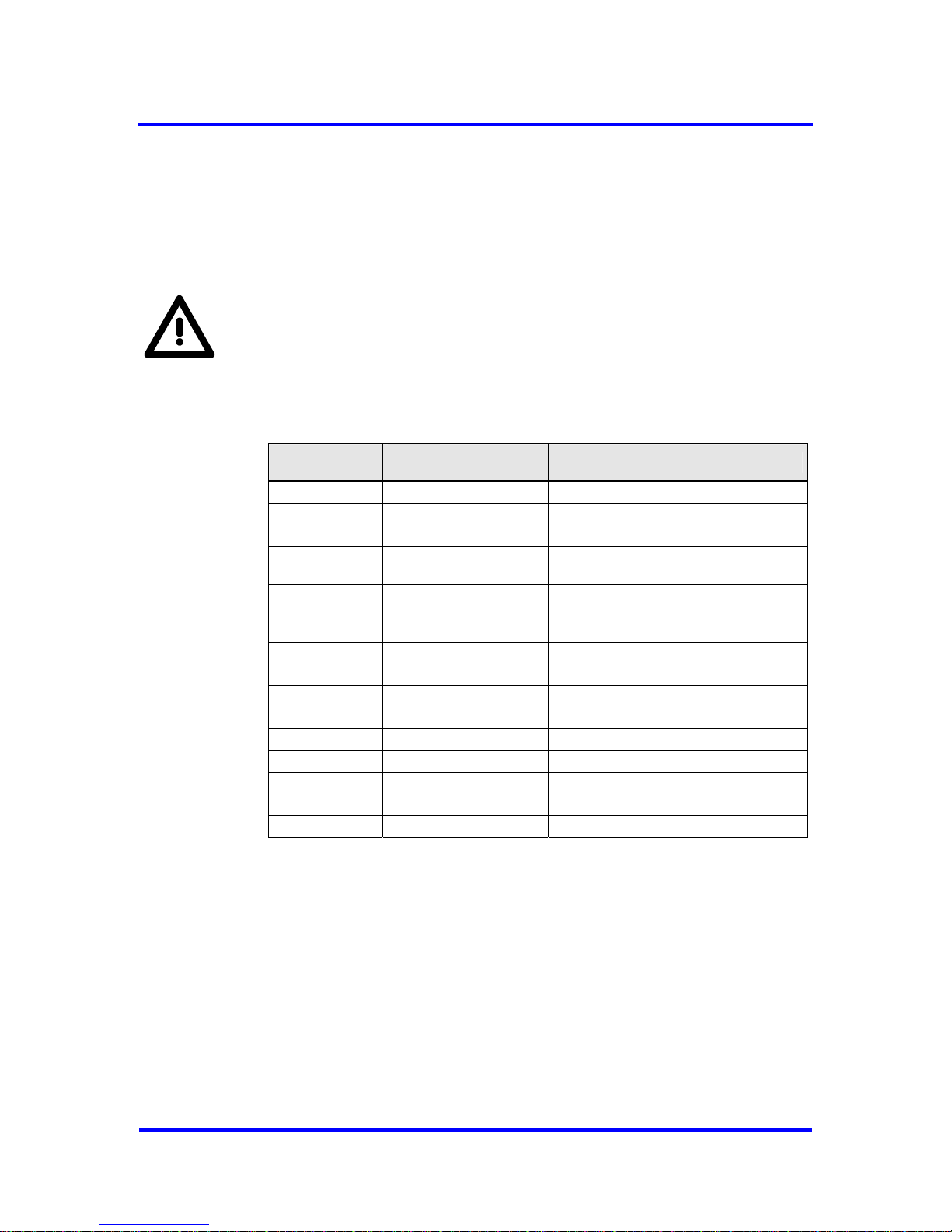
8 Hardware Interface
used in the synchronous Intel mode. One figure shows the minimum configuration of a system with the VPC3+C, where the chip is connected to an
EPROM version of the controller. Only a clock generator is necessary as an
additional device in this configuration. If a controller is to be used without an
integrated program memory, the addresses must be latched for the external
memory.
Notes:
If the VPC3+C is connected to an 80286 or similar processor, it must be
taken into consideration that the processor carries out word accesses. That
is, either a ‘swapper’ is necessary that switches the characters out of the
VPC3+C at the correct byte position of the 16-bit data bus during reading or
the least significant address bit is not connected and the 80286 must read
word accesses and evaluate only the lower byte.
Name
Input/
Output
Type Comments
DB(7..0) I/O Tristate High-resistance during RESET
AB(10..0) I AB(10) has a pull down resistor.
MODE I Configuration: syn/async interface
XWR/E_CLOCK
AB11
I
Intel: Write Sync. Motorola: E-Clk
AB11 (Asynchronous Motorola Mode)
XRD/R_W I Intel: Read Motorola: Read/Write
XCS
AB11
I
Chip Select
AB11 (Synchronous Intel Mode)
ALE/AS
AB11
I Intel/Motorola: Address Latch Enable
AB11 (Async. Intel / Sync. Motorola Mode)
DIVIDER I Scaling factor 2/4 for CLKOUT 2/4
X/INT O Push/Pull Polarity programmable
XRDY/XDTACK O Push/Pull * Intel/Motorola: Ready-Signal
CLK I 48 MHz
XINT/MOT I Setting: Intel/Motorola
CLKOUT2/4 O Push/Pull 24/12 MHz
RESET I Schmitt-Trigger Minimum of 4 clock cycles
Figure 8-2: Microprocessor Bus Signals
* Due to compatibility reasons to existing competitive chips the XRDY/XDTACK output of the
VPC3+C has push/pull characteristic (no tristate!).
70 Revision 1.03
VPC3+C
User Manual
Copyright © profichip GmbH 2004-2006
Page 71

Hardware Interface 8
Synchronous Intel Mode
In this mode Intel CPUs like 80C51/52/32 and compatible processor series
from several manufacturers can be used.
Synchronous bus timing without evaluation of the XREADY signal
8-bit multiplexed bus: ADB7..0
The lower address bits AB7..0 are stored with the ALE signal in an in-
ternal address latch.
The internal CS decoder is activated. VPC3+C generates its own CS
signal from the address lines AB10..3. The VPC3+C selects the
relevant address window from the AB2..0 signals.
A11 from the microcontroller must be connected to XCS (pin 1) in 4K
Byte mode as this is the additional address bus signal in this mode. In
2K Byte mode this pin is not used and should be pulled to VDD.
Asynchronous Intel Mode
In this mode various 16-/8-bit microcontroller series like Intel’s x86,
Siemens 80C16x or compatible series from other manufacturers can be
used.
Asynchronous bus timing with evaluation of the XREADY signal
8-bit non-multiplexed bus: DB7..0, AB10..0 (AB11..0 in 4K Byte mode)
The internal VPC3+C address decoder is disabled, the XCS input is
used instead.
External address decoding is always necessary.
External chip select logic is necessary if not present in the microcon-
troller
A11 from the microcontroller must be connected to ALE/AS (pin 24) in
4K Byte mode as this is the additional address bus signal in this mode.
In 2K Byte mode this pin is not used and should be pulled to GND.
Asynchronous Motorola Mode
Motorola microcontrollers like the HC16 and HC916 can be used in this
mode. When using HC11 types with a multiplexed bus the address signals
AB7..0 must be generated from the DB7..0 signals externally.
Asynchronous bus timing with evaluation of the XREADY signal
8-bit non-multiplexed bus: DB7..0, (AB11..0 in 4K Byte mode)
The internal VPC3+C address decoder is disabled, the XCS input is
used instead.
Chip select logic is available and programmable in all microcontrollers
mentioned above.
AB11 must be connected to XWR/E_CLOCK (pin 2) in 4K Byte mode
as this is the additional address bus signal in this mode. In 2K Byte
mode this pin is not used and should be pulled to GND.
VPC3+C User Manual
Revision 1.03 71
Copyright © profichip GmbH 2004-2006
Page 72

8 Hardware Interface
Synchronous Motorola Mode
Motorola microcontrollers like the HC11 types K, N, M, F1 or the HC16- and
HC916 types with programmable E_Clock timing can be used in this mode.
When using HC11 types with a multiplexed bus the address signals AB7..0
must be generated from the DB7..0 signals externally.
Synchronous bus timing without evaluation of the XREADY signal
8-bit non-multiplexed bus: DB7..0, AB10..0 (AB11..0 in 4K Byte mode)
The internal VPC3+C address decoder is disabled, the XCS input is
used instead.
For microcontrollers with chip select logic (K, F1, HC16 and HC916),
the chip select signals are programmable regarding address range, priority, polarity and window width in the write cycle or read cycle.
For microcontrollers without chip select logic (N and M) and others, an
external chip select logic is required. This means additional hardware
and a fixed assignment.
If the CPU is clocked by the VPC3+C, the output clock pulse (CLKOUT
2/4) must be 4 times larger than the E_Clock. That is, a clock pulse signal must be present at the CLK input that is at least 10 times larger than
the desired system clock pulse (E_Clock). The Divider-Pin must be
connected to ‘0’ (divider 4). This results in an E_Clock of 3 MHz.
AB11 must be connected to ALE/AS (pin 24) in 4K Byte mode as this is
the additional address bus signal in this mode. In 2K Byte mode this pin
is not used and should be pulled to GND.
72 Revision 1.03
VPC3+C
User Manual
Copyright © profichip GmbH 2004-2006
Page 73
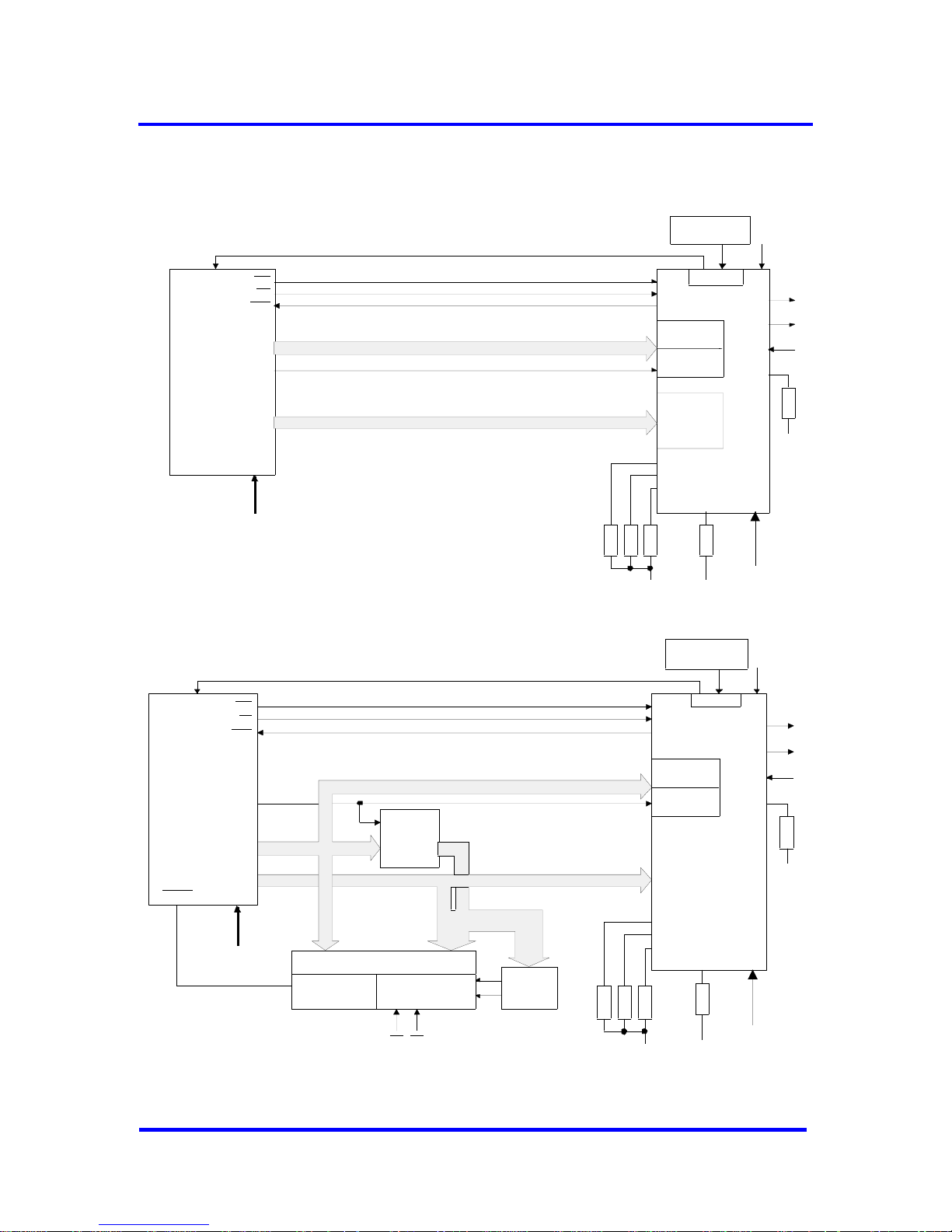
Hardware Interface 8
8.1.3 Application Examples (Principles)
AB 1 5 ...8
Clock-Generator
48MHz
80C32/
C501
Port 0
ALE
Port 2
CLK
XW R
XRD
X/INT
AB8
AB9
AB10
1K 1K
3K 3
Mod e
VDD
RT S
TxD
Rx D
XCTS
1K
GND
Reset
VPC3+
AB 7.. 0
Decoder
DB 7..0
Data
DB 7..0
Address-Latch
A / D 7 ...0
WR
RD
INT0
1K
Clockdivider
DIV IDE R
VPC3+
Reset
(0000 0XXX)
GND
Figure 8-3: Low Cost System with 80C32
WR
RD
INT0
48 MHz
80C32
20/16 MHz
Po rt 0
Port 2
CLK
XW R
XRD
X/INT
AB8
AB9
AB10
1K 1K
3K 3
Mode
GND VDD
RT S
TxD
Rx D
XC TS
1K
GND
ALE
EPROM
64kB
RAM
32kB
AddressDecoder
Reset
PSEN
VPC3+
RD W R
DB 7..0
Data
DB 7..0
Address-Latch
Clockdivider
DIVIDE R
1K
(0000 0XXX)
VPC3+
Reset
Address-
Latch
A/D 7..0
AB 15..8
AB 15..0
Clock-Generator
Figure 8-4: 80C32 System with External Memory
VPC3+C User Manual
Revision 1.03 73
Copyright © profichip GmbH 2004-2006
Page 74
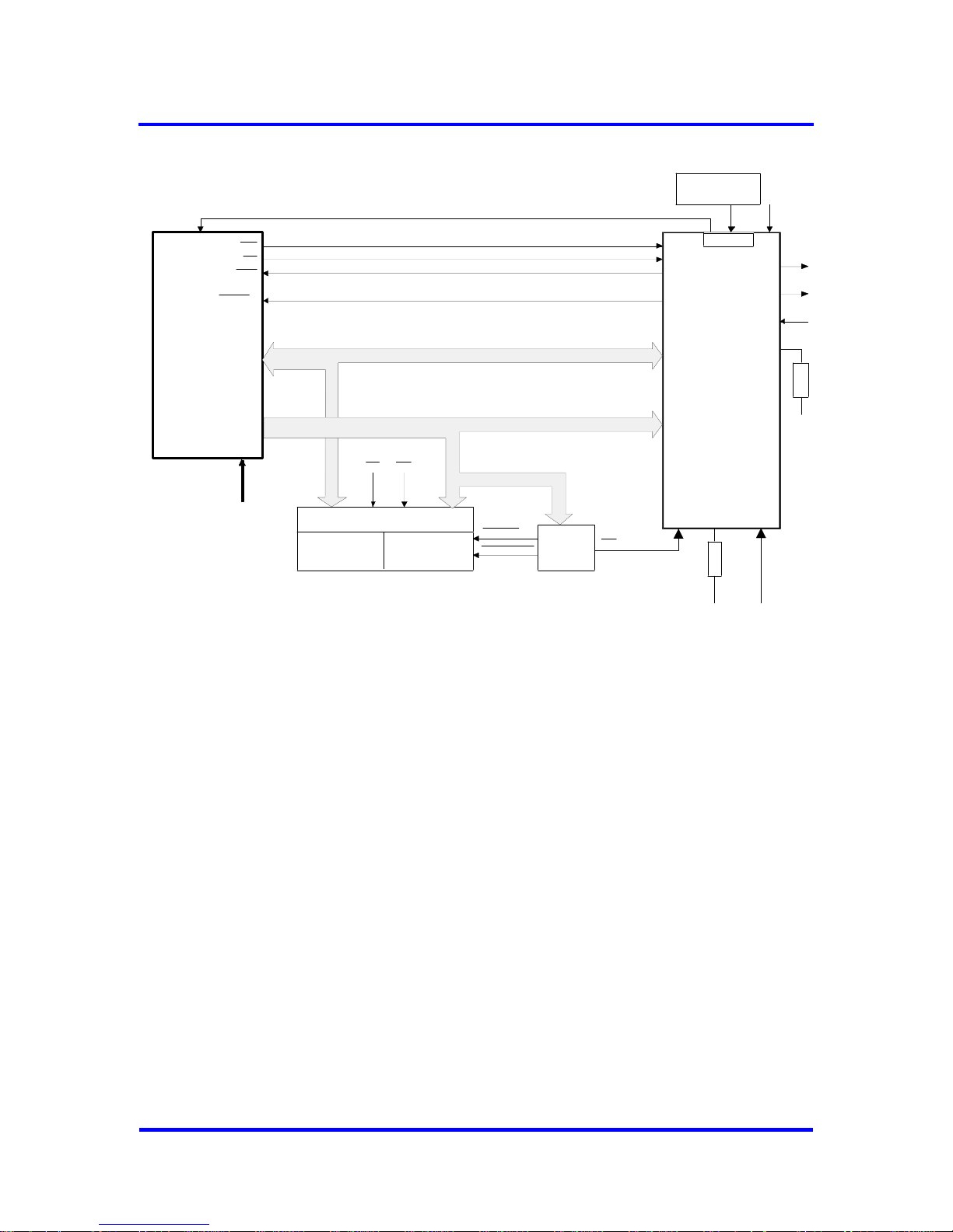
8 Hardware Interface
WR
RD
INT R
Readylogic
Clockgenerator
48 MHz
80286
+
Buscontr.
(82288) +
82244
DB
AB
CLK
XWR
XRD
X/INT
XREADY
3K3
Mode
GND
VPC3+
Reset
RTS
TxD
RxD
XCTS
1K
GND
EPROM
64kB
RAM
32kB
address
decoder
Reset
VPC3+
12/24 MHz
clockdivider
DIVIDER
AB 23..0
AB 12..1
DB 15..0
DB 7..0
XCS
CS
CSRAM
CSEPROM
driver, control logic
DB(7..0)
AB(10..0)
RD WR
Figure 8-5: 80286 System (X86 Mode)
74 Revision 1.03
VPC3+C
User Manual
Copyright © profichip GmbH 2004-2006
Page 75
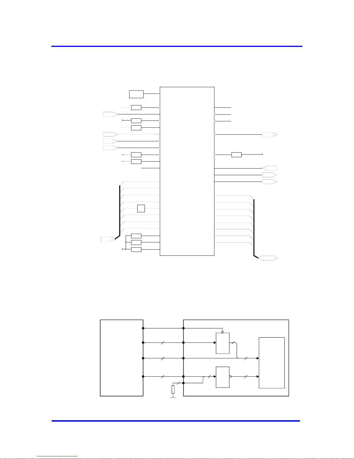
Hardware Interface 8
8.1.4 Application with 80C32 (2K Byte RAM Mode)
CLK
RESET
XCS
MODE
ALE
XWR
XRD
XTEST0
XTEST1
DIVIDER
48 MHz
1K
3K3
3K3
3K3
GND
VDD
µC
µC
µC
A
B(15..8)
connect to
VDD or GND
XWR
XRD
5
8
36
CLK2
XDATAEX
1
23
XREADY
24
2
4
34
35
3
44
43
41
40
37
42
29
10
X/INT
XCTS
RXD
RTS
TXD
32
31
V
PC3+
µC
1K
RS485
RS485
RS485
7
13
14
9
33
30
27
26
11
12
15
16
21
22
19
20
25
µC
DB(7..0)
GND
VDD
LED for Data_Exchange
XINT/MOT
VDD
µC
3K3
VDD
AB0
AB1
AB2
AB3
AB4
AB5
AB7
AB10
DB0
DB1
DB2
DB3
DB5
AB6
DB4
AB8
AB9
DB6
DB7
µC
ADB0
ADB1
ADB2
ADB3
ADB6
ADB7
AB8
AB9
AB10
AB11
AB12
AB13
ADB4
ADB5
AB14
AB15
1K
1K
1K
GND
1
Figure 8-6: 80C32 Application in 2K Byte mode
ctivated when the address inputs AB[10..3] of
the example above the start address of the VPC3+C is set to 1000H.
The internal chipselect is a
the VPC3+C are set to '0'.
In
CS
decoder
4.0 KB
RAM
address
latch
8
8
5
311
1
ALE
AD[7..0]
AB[10..8]
all bits
zero
AB[15..11]
internal chip
select
internal address
ALE
DB[7..0]
AB[2..0]
Processor VPC3+ B
AB[7..3]
AB[10..8]
8
3
Figure 8-7: Internal Chipselect Generation in Synchronous Intel Mode, 2K Byte RAM
VPC3+C User Manual
Revision 1.03 75
Copyright © profichip GmbH 2004-2006
Page 76
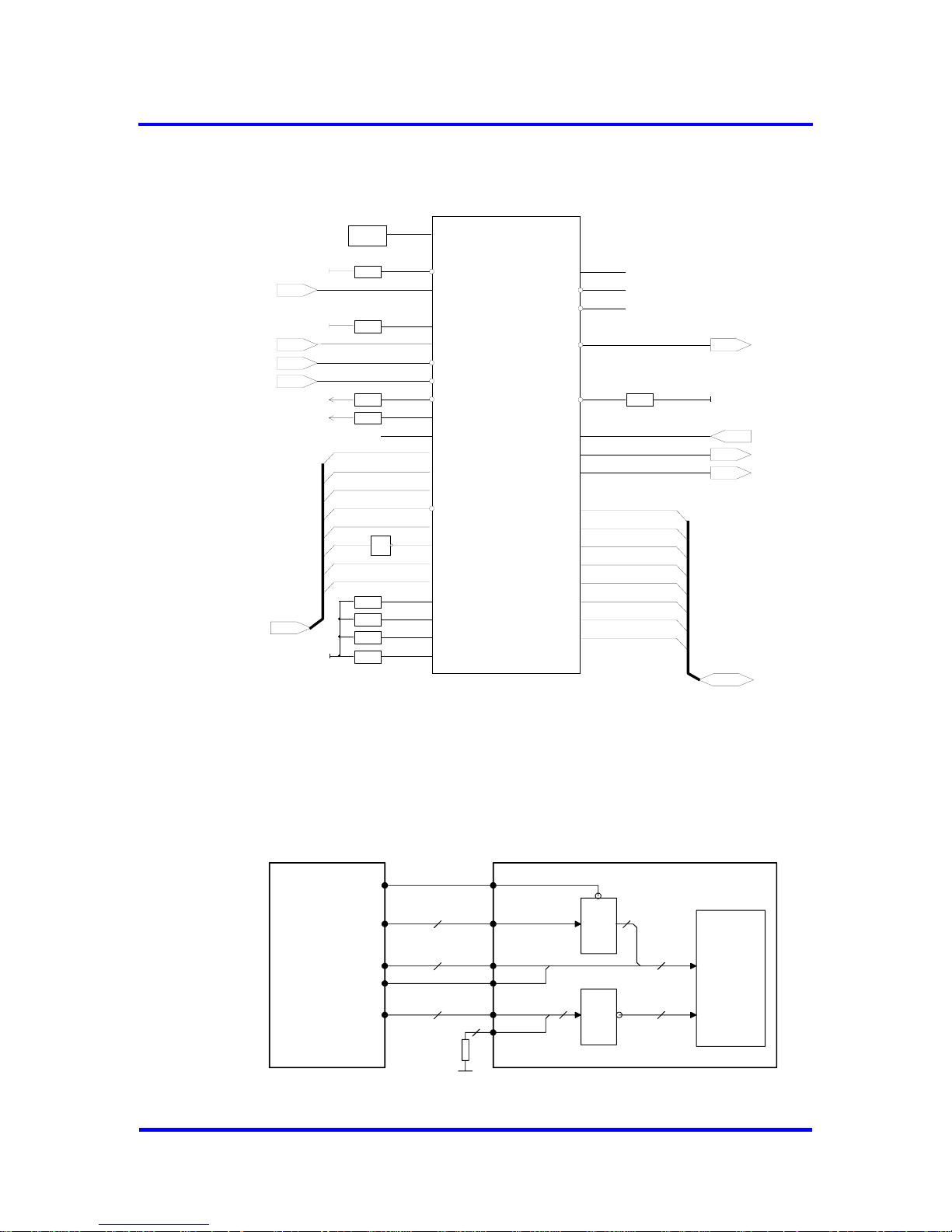
8 Hardware Interface
8.1.5 Application with 80C32 (4K Byte RAM Mode)
V
PC3+
CLK
RESET
MODE
ALE
XWR
XRD
XTEST0
XTEST1
DIVIDER
48 MHz
1K
3K3
3K3
3K3
GND
VDD
µC
µC
µC
5
8
1
43
41
29
CLK2
XDATAEX
RTS
TXD
A
B(15..8)
connect to VDD or GND
XWR
XRD
36
23
24
2
4
34
35
3
XREADY
X/INT
XCTS
RXD
40
37
42
32
31
25
10
µC
1K
RS485
RS485
RS485
7
13
27
26
11
21
14
9
33
30
GND
VDD
VDD
12
15
16
19
20
22
µC
DB(7..0)
AB0
AB1
AB2
AB8
LED for Data_Exchange
/MOTXINT
µC
XCS/AB11
AB3
AB4
AB5
AB6
AB7
DB0
DB1
DB2
DB3
DB4
DB5
AB9
AB10
DB6
DB7
µC
ADB0
ADB6
AB8
AB9
AB10
AB11
ADB1
ADB2
ADB3
ADB4
ADB5
AB12
AB13
AB14
AB15
ADB7
1K
1K
1K
GND
1
1K
44
Figure 8-8: 80C32 Application in 4K Byte mode
The internal chipselect is activated when the address inputs AB[10..3] of
the VPC3+C are set to '0'.
In the example above the start address of the VPC3+C is set to 2000H.
CS
decoder
4.0 KB
address
latch
8
ALE
AD[7..0]
ALE
Processor VPC3+ B
RAM
8
312
B[10..8]
internal address
DB[7..0]
AB[2..0]
XCS/A11
4 1
all bits
zero
AB[15..12]
internal chip
select
A
AB[11]
AB[6..3]
AB[10..7]
8
4
Figure 8 s Intel Mode, 4K Byte RAM -9 : Internal Chipselect Generation in Synchronou
76 Revision 1.03
VPC3+C
User Manual
Copyright © profichip GmbH 2004-2006
Page 77
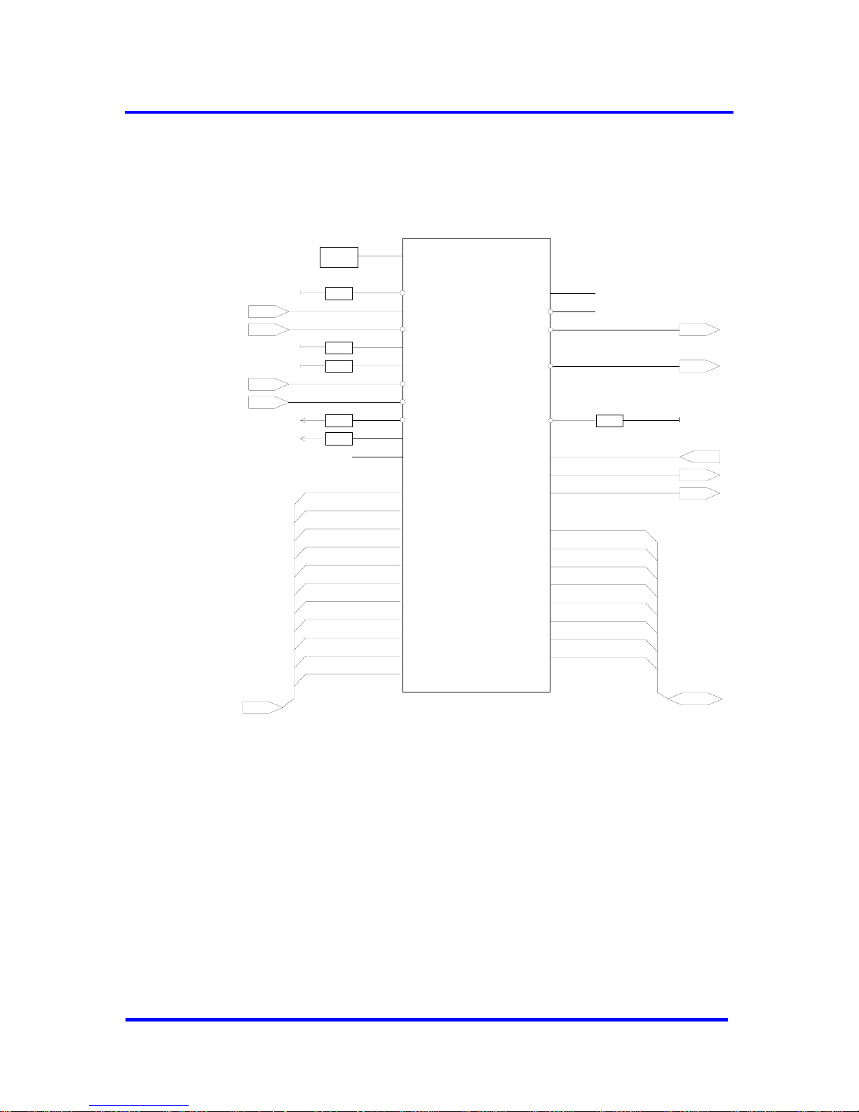
Hardware Interface 8
8.1.6 Applicati w 1on ith 80C 65
CLK
RESET
XCS
MODE
ALE
XWR
XRD
XTEST0
XTEST1
DIVIDER
48 MHz
1K
1K
1K
3K3
3K3
GND
VDD
µC
µC
µC
µC
AB(10..0)
connect to
VDD or GND
AB0
AB1
AB2
AB3
AB4
AB5
AB6
AB7
AB8
AB9
AB10
XWRL
XRD
µC
5
8
36
1
23
24
2
4
34
35
3
44
43
41
40
37
42
32
31
29
25
10
CLK2
XDATAEX
XREADY
X/INT
XCTS
RXD
RTS
TXD
VPC3+
µC
1K
RS485
RS485
RS485
7
13
14
9
33
30
27
26
11
12
15
16
19
20
21
22
µC
DB(7..0)
DB0
DB1
DB2
DB3
DB4
DB5
DB6
DB7
GND
GND
GND
VDD
AB0
AB1
AB2
AB3
AB4
AB5
AB6
AB7
AB8
AB9
AB10
DB0
DB1
DB2
DB3
DB4
DB5
DB6
DB7
LED for Data_Exchange
XINT/MOT
µC
Figure 8-10: 80C165 Application
8.2 Dual Port RAM Controller
The internal 4K Byte RAM of the VPC3+C is a single-port RAM. An
integrated Dual-Port RAM controller, however, permits an almost
simultaneous access of both ports (bus interface and microsequencer
interface). When there is a simultaneous access of both ports, the bus
interface has priority. This guarantees the shortest possible access time. If
the VPC3+C is connected to a microcontroller with an asynchronous
interface, the controller can evaluate the Ready signal.
VPC3+C User Manual
Revision 1.03 77
Copyright © profichip GmbH 2004-2006
Page 78
8 Hardware Interface
8.3 UART
nverts the parallel data structure into a serial data flow.
-Send (RTS) is generated before the first character. The
fter each character.
he receiver converts the serial data flow into the parallel data structure
e l he four-fold transmission speed. Stop
s ('Dis_Stop_Control = 1' in
ter 0 or Set_P r DP). One requirement of the
is tha tates are permitted between the
The transmitter ensures that this
he synchronization of the receiver starts with the falling edge of the start
nd the stop bit are also scanned in the middle of
e bit-time. To compensate for the synchronization error, a repeater gen-
ion of the stop bit at a four-fold scan rate. In this case
ould be parameterized with 'Dis_Start_Control = 1' (in Mode
et_Prm telegram for DP) in order to increase the permissible
8.4 ASIC T
and I/O pins can be switched to the high-resistance state via
test pin. An additional XTEST1 input is provided to test the
The transmitter co
Signal Request-to
XCTS input is available for connecting a modem. After RTS active, the
transmitter must hold back the first telegram character until the modem activates XCTS. XCTS is checked again a
T
and scans th serial data f ow with t
bit testing can be switched off for test purpose
Mode Regis rm telegram fo
PROFIBUS protocol t no rest s
telegram characters. VPC3+C
specification is maintained.
T
bit. The start bit is checked again in the middle of the bit-time for low level.
The data bits, the parity a
th
erates a ±25% distort
the VPC3+ sh
Register 0 or S
distortion of the stop bit.
est
All output pin
the XTEST0
s
chip on automatic test devices (not in the target hardware environment!).
Pin Name Value Function
VSS (GND) All outputs high-resistance
34 XTEST0
VDD Normal VPC3+ function
VSS (GND) Various test modes
35 XTEST1
VDD Normal VPC3+ function
Figure 8-11: Test Ports
78 Revision 1.03
VPC3+C
User Manual
Copyright © profichip GmbH 2004-2006
Page 79
PROFIBUS Interface 9
9 PROFIBUS Interface
the
terface drivers.
9.1 Pin Assignment
The data transmission is performed in RS485 operating mode (i.e., physical
S485). The VPC3+C is connected via the following signals to R
galvanically isolated in
Signal Name Input/Output Function
RTS Output Request to send
TXD Output Sending data
RXD Input Receiving data
Figure 9-1: PROFIBUS Signals
The PROFIBUS interface is a 9-way, sub D, plug connector with the
following pin assignment.
Pin 1 - Free
Pin 2 - Free
Pin 3 - B line
Pin 4 - Request to send (RTS)
Pin 5 - Ground 5V (M 5 )
Pin 6 - Potential 5V (floating P5 )
Pin 7 - Free
Pin 8 - A line
Pin 9 - Free
The cable shield must be connected to the plug connector housing.
The free pins are described as optional in IEC 61158-2.
CAUTION:
The pin names A and B on the plug connector refer to the signal names in
the RS485 standard and not the pin names of driver ICs.
Keep the wires from driver to connector as short as possible.
VPC3+C User Manual
Revision 1.03 79
Copyright © profichip GmbH 2004-2006
Page 80
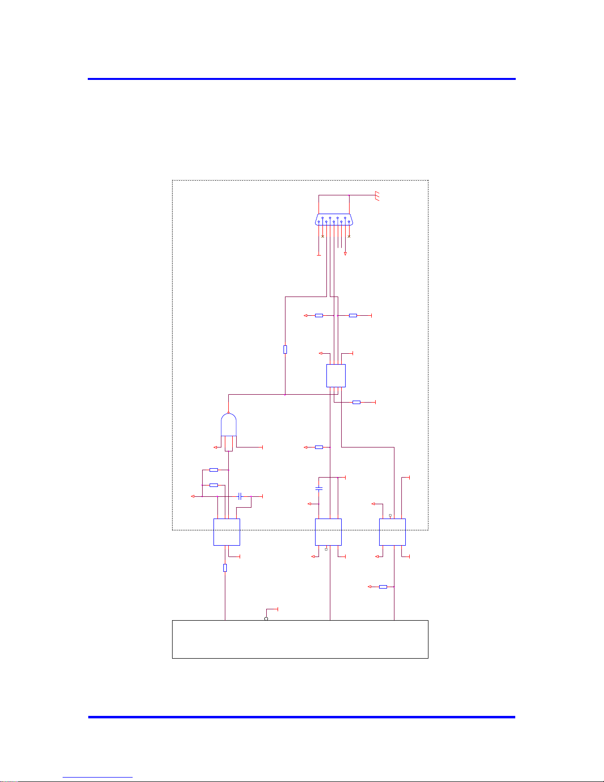
9 PROFIBUS Interface
9.2 Example for the RS485 Interf
To minimize the capacity of the
ace
bus lines the user should avoid additional
The typical capa n should be 15...25 pF.
Figure 9-2: Example for the RS485 Interface
capacities. city of a bus statio
VCC_I SO
33
R9
22K
12
R35
330R
12
R36
0R68
12
GND_I SO
R2
330R
1 2
C1
100
080
n
5
1 2
GND_I SO
GND_I SO
RTS
GND
VCC_I SO
R3
1K
9
12
SHIELD
VCC_I SO
30
VCC_ISO
VCC
R4
100K
12
RXD
GND
RTS
R40
470R
1 2
VPC3+C
GND_I SO
26
VCC
R34
680R
12
M24V
VCC_I SO
VCC
IC1
74AHCT1G00
1
2
4
53
B
GND_I SO
R3
100K
12
IC2
DS75176
SO08
124
678
5
3
R
RE#
D
A
B
VCC
GND
DE
GND
C15
100n
0805
1 2
VCC_I SO
GND_I SO
IC8
HCPL0710
SO08
124
768
5
VCC1
VI
GND1
GND2NCVO
VCC2
27
IC6
HCP
SO08
L0710
124
768
5
VCC1
VI
1
NC
VO
VCC2
GND2
GND
TXD
IC7
HCP
SO08
L0601
2
3
768
5
VE
VO
VCC
GND
A
K
GND_I SO
A
X1
SUBD_BU9
11
10
162738495
P24V
GND_I SO
XCTS
GND
VCC_I SO
VCC_I SO
80 Revision 1.03
VPC3+C
User Manual
Copyright © profichip GmbH 2004-2006
Page 81
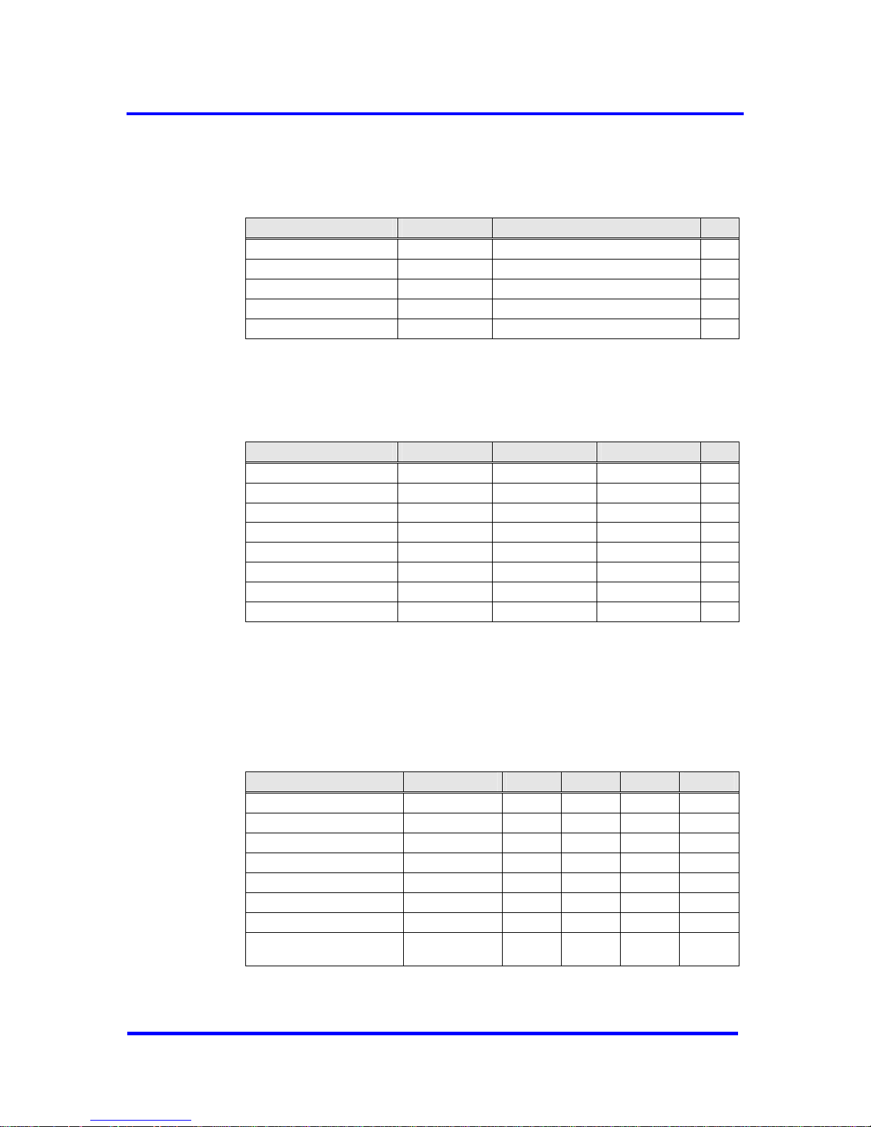
Operational Specifications 10
10 Operational Specifications
10.1 Absolute Maximum Ratings
Parameter Symbol Limits Unit
DC supply voltage V
DD
-0.3 to 6.0 V
Input voltage V -0.3 +0.3
I
to V
DD
V
Output voltage V
O
-0.3 +0.3 to V
DD
V
DC output current I
O
See 10-4 A Figure m
Storage temperature T
st
-4
ore
0 to +125 °C
F bsolute Maximum Ratinigure 10-1: A gs
10.2 Recommended Operating Conditions
Parameter Symbol MIN MAX Unit
DC supply voltage V
DD
3.00 5.50 V
Static supply current I
DD
100
1)
µA
Circuit ground V
SS
0 0 V
Input voltage V
I
0 5.50 V
Input voltage (HIGH level) V
IH
5.50 V 0.7 V
DD
Input voltage (LOW level) V
IL
0.30 V
DD
V
Output voltage V
O
V
DD
0 V
Ambient temperature T
A
+85 -40 °C
1)
:
Static I
DD
current is exclusivel
measured with the clock stop
y of inp utput drive requir ts an
ped and all inputs tied to V
DD
or VSS.
ating C itions
10.3 General DC Characteristics
ut/o emen d is
Figure 10-2: Recommended Oper ond
Symbo M T M UParameter l IN YP AX nit
Input LOW current I
IL
-1 +1 µA
Input HIGH current I
IH
+-1 1 µA
Tri-state leakage current I
OZ
-10 +1 0 µA
Current consumption (3.3V) I
A
45 mA
Current consumption (5V) I
A
90 mA
Input capacitance C
IN
5 pF
Output capacitance C
OUT
5 pF
Bi-directional buffer
capacitance
C
BID
5 pF
Figure 10-3: General DC Characteristics
VPC3+C User Manual
Revision 1.03 81
Copyright © profichip GmbH 2004-2006
Page 82
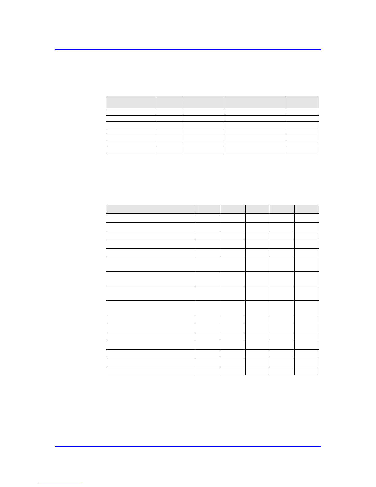
10 Operational Specifications
10.4 Ratings for the Output Drivers
Signal Direction
Driver
Ty pe
Driver gth Stren
Max. Cap.
Load
DB 0-7 I/O Tristate 8 100pF mA
RTS O Pus l 8m 50ph/Pul A F
TXD O Tristate 8m 50pA F
X/INT O Push/Pull 4mA 50pF
XREADY/XDTACK O Push/Pull 4mA 50pF
XDATAEXCH O Push/Pull 8mA 50pF
CLKOUT2/4 O Push/Pull 8mA 100pF
Figure 10-4: Ratings for the Output Drive
10.5 DC Electrical Characteristics Specification for 5V Operation
rs
Parameter Sy ol MIN TYP M mb AX Unit
DC supply voltage V
DD
4.50 5.00 5.50 V
CMOS input voltage LOW level 0.3 V
ILC
0 V
DD
V
CMOS input voltage HIGH level V
IHC
0 V.7 V
DD
DD
V
Output voltage LOW level V
OL
0 .4 V
Output voltage HIGH level V
OH
3.5 V
CMOS Schmitt Trigger
negative going threshold voltage
1
V
T-
1.5 .8 V
CMOS Schmitt Trigger
V
3.2
positive going threshold voltage
T+
3.5 V
TTL Schmitt Trigger
going threshold voltage
V
T-
0.9 1.1 V
negative
TTL Schmitt Trigger
positive going threshold voltage
V
T+
1.9 2.1 V
Input LOW current I
IL
-1 +1 µA
Input HIGH current I
IH
-1 +1 µA
Tri-state leakage current I
OZ
-10 ±1 +10 µA
Output current LOW level, 4mA cell I
OL
4.0 mA
Output current HIGH level, 4mA cell I
OH
-4.0 mA
Output current LOW level, 8mA cell I
OL
8.0 mA
Output current HIGH level, 8mA cell I
OH
-8.0 mA
Figure 10-5: DC Specification of I/O Drivers for 5V Operation
82 Revision 1.03
VPC3+C
User Manual
Copyright © profichip GmbH 2004-2006
Page 83
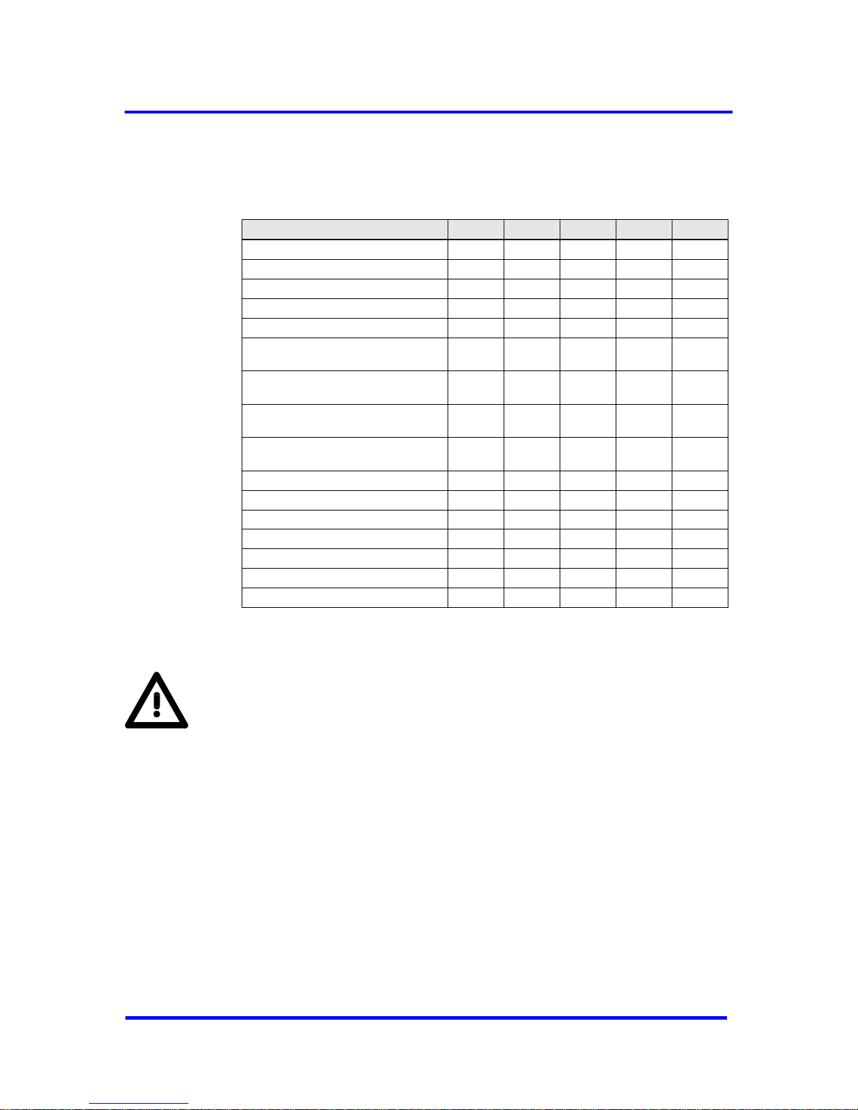
Operational Specifications 10
10.6 DC Electrical Characteristics Specification for 3.3V Operation
Parameter Symbol MIN TYP MAX Unit
DC supply voltage V
DD
3.00 3.30 3.60 V
CMOS input voltage LOW level V
ILC
0 0.3 V
DD
V
CMOS input voltage HIGH level V
IHC
0.7 V
DD
5.50 V
Output voltage LOW level V
OL
0.4 V
Output voltage HIGH level V
OH
2.4 V
CMOS Schmitt Trigger
negative going threshold voltage
V
T-
0.8 V
CMOS Schmitt Trigger
positive going threshold voltage
V
T+
2.7 V
TTL Schmitt Trigger
d voltage
V
T-
0.6 V
negative going threshol
TTL Schmitt Trigger
ld voltage
V
T+
1 V
positive going thresho
.7
Input LOW current I
IL
-1 +1 µA
Input HIGH current I
IH
-1 +1 µA
Tri-state leakage current I
OZ
-10 ±1 +10 µA
Output current LOW level, 4mA cell I
OL
+2.8 mA
Output current HIGH level, 4mA cell I
OH
-2.8 mA
Output current LOW level, 8mA cell I
OL
+5.6 mA
Output current HIGH level, 8mA cell I
OH
-5.6 mA
Figure 10-6: DC Specification of I/O Drivers for 3.3V Operation
N
For 3.3V operation the VPC3+C is equipped with 5V tolerant inputs except
f
t
or 3.3V operation the guaranteed minimum output current is 70% of that
otes:
or the clock pin CLK. When using 3.3V supply voltage the clock input needs
o be 3.3V level.
F
for 5V operation mode.
VPC3+C User Manual
Revision 1.03 83
Copyright © profichip GmbH 2004-2006
Page 84
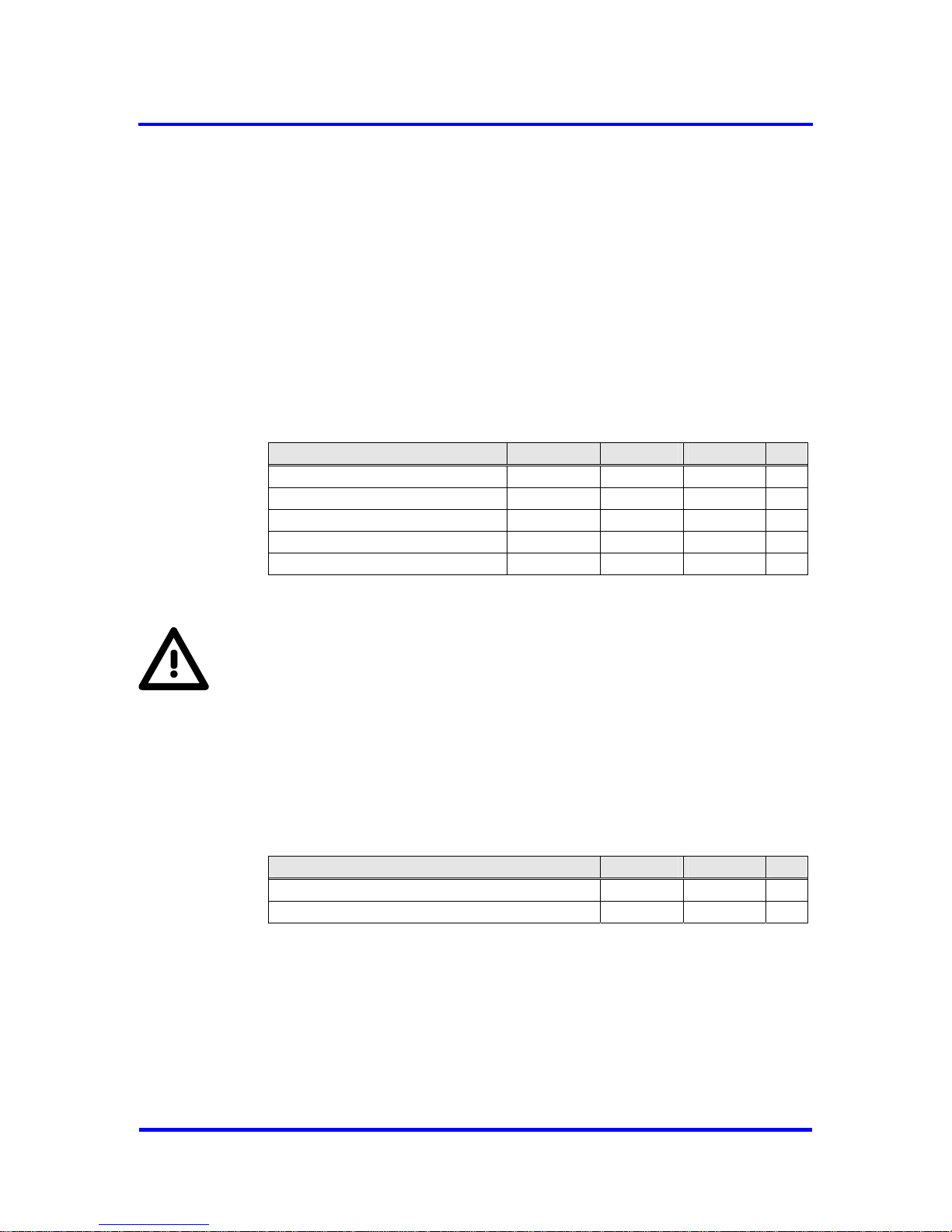
10 Operational Specifications
10.7 Timing Characteristics
10.7.1 System
lock
lock frequency is 48 MHz. Distortion of the clock signal is permissible up
to a ratio of 30:70 at the threshold levels 0.9 V and 2.1 V.
All signals beginning with ‘X’ are ‘low active’. All timing values are based on
the capacitive loads specified in the table above.
Bus Interface
C
C
Parameter Symbol MIN MAX Unit
Clock period T 20.83 20.83
Clock high time T
CH
6.25 14.6 ns
Clock low time T
CL
6.25 14.6 ns
Clock rise time T
CR
4 ns
Clock fall time T
CF
4 ns
Figure 10-7: Clock Timing
Note:
For 3.3V operation the VPC3+C is equipped with 5V tolerant inputs except
for the clock pin CLK. When using 3.3V supply voltage the clock input needs
to be 3.3V level.
Interrupt:
After acknowledging an interrupt with EOI, the interrupt output of the
VPC3+C is deactivated for at least 1 us or 1 ms depending on the bit
EOI_Time_Base in Mode Register 0.
Parameter MIN MAX Unit
Interrupt inactive time EOI_Timebase = ‘0’ 1 1 µs
Interrupt inactive time EOI_Timebase = ‘1’ 1 1 ms
Figure 10-8: End-of-Interrupt Timing
Reset:
VPC3+C requires a minimum reset phase of 100 ns at power-on.
84 Revision 1.03
VPC3+C
User Manual
Copyright © profichip GmbH 2004-2006
Page 85
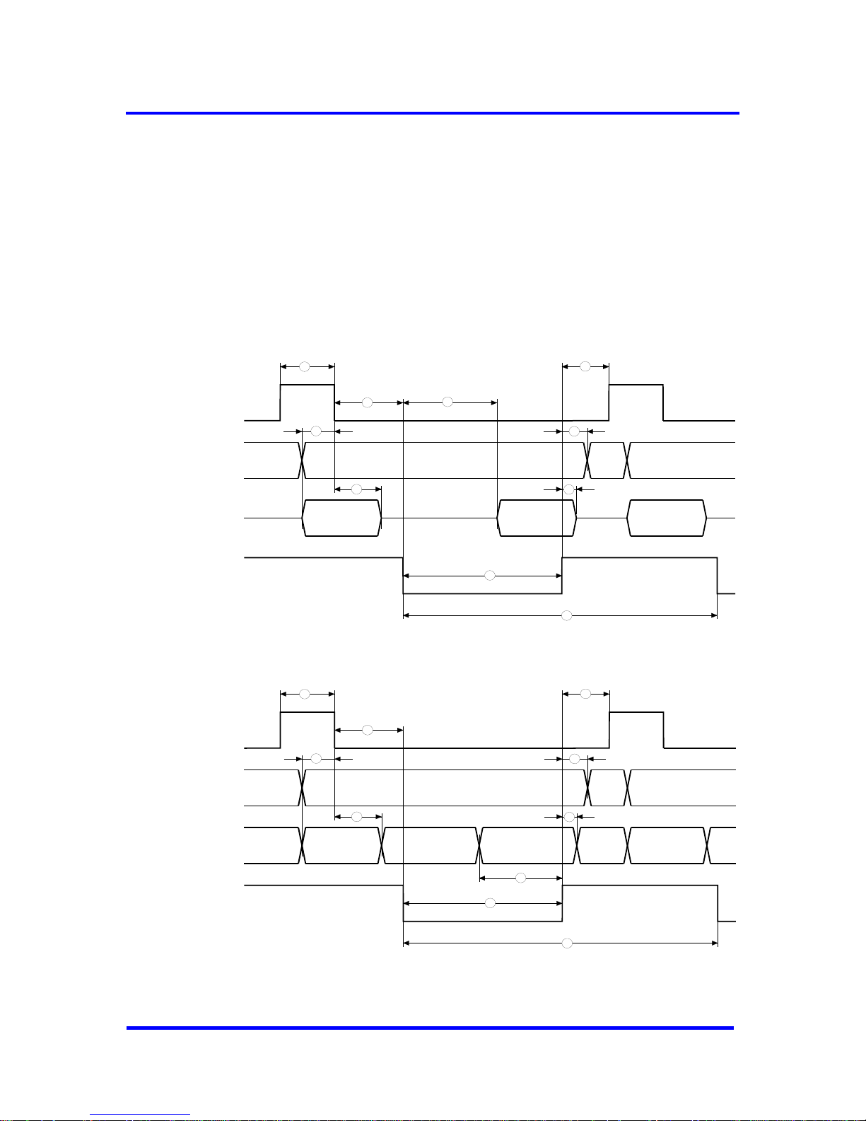
Operational Specifications 10
10 .2 the Synchronous Intel Mode
he synchronous Intel mode, 3+C latches the least significant
ith the falling edge
icant address bits on the address bus. An inter
al is generated from the most significant addre s bits e
t for an access to the VPC3+C is generated from the fa g ed of
read signal (XRD) and from the rising edge of the write signal (XWR).
.7 Timing in
In t the VPC
addresses w
expects the most signif
of ALE. At the same time, the VPC3+C
nal
. Thchipselect sign s
reques llin ge
the
ALE
AB10..0
DB7..0
XRD
valid
va d
data valid
address
address
li
1
2
3
4
5
6
10
9
8
7
Figure 10-9: Synchronous Intel Mode, READ (XWR = 1)
ALE
AB10..0
DB7..0
XWR
valid
valid
data valid
address
address
1
11
3
15
13
12
10
15
8
14
Figure 10-10: Synchronous Intel Mode, WRITE (XRD = 1)
VPC3+C User Manual
Revision 1.03 85
Copyright © profichip GmbH 2004-2006
Page 86
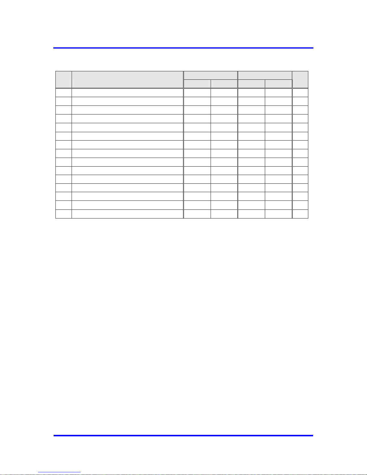
10 Operational Specifications
VDD = 3.3 V VDD = 5 V
No. Parameter
MIN MAX MIN MAX
Unit
1 ALE pulsewidth 10 10 ns
2
ALE ↓ to XRD ↓
20
20 ns
3
Address to ALE ↓ setuptime
10
10 ns
4
Address holdtime after ALE ↓
10
10 ns
5
XRD ↓ to dat
ns
a valid
103
97
6 XRD pulsewi h 115 115 ns dt
7
XRD ↑ to AL ↑
10
10 ns
E
8
address (AB7..0) holdtime after XRD/XWR ↑
5
5 ns
9
data holdtime after XRD ↑
4 16
4 13 ns
10 XRD / XWR cycletime 155 155 ns
11
ALE ↓ to XWR ↓
20
20 ns
12 XWR pulsewidth 83 83 ns
13
data setuptime to XWR ↑
10
10 ns
14
XWR ↑ to ALE ↑
10
10 ns
15
data holdtime after XWR ↑
10
10 ns
Figure 10-11: Timing, Synchronous Intel Mode
86 Revision 1.03
VPC3+C
User Manual
Copyright © profichip GmbH 2004-2006
Page 87
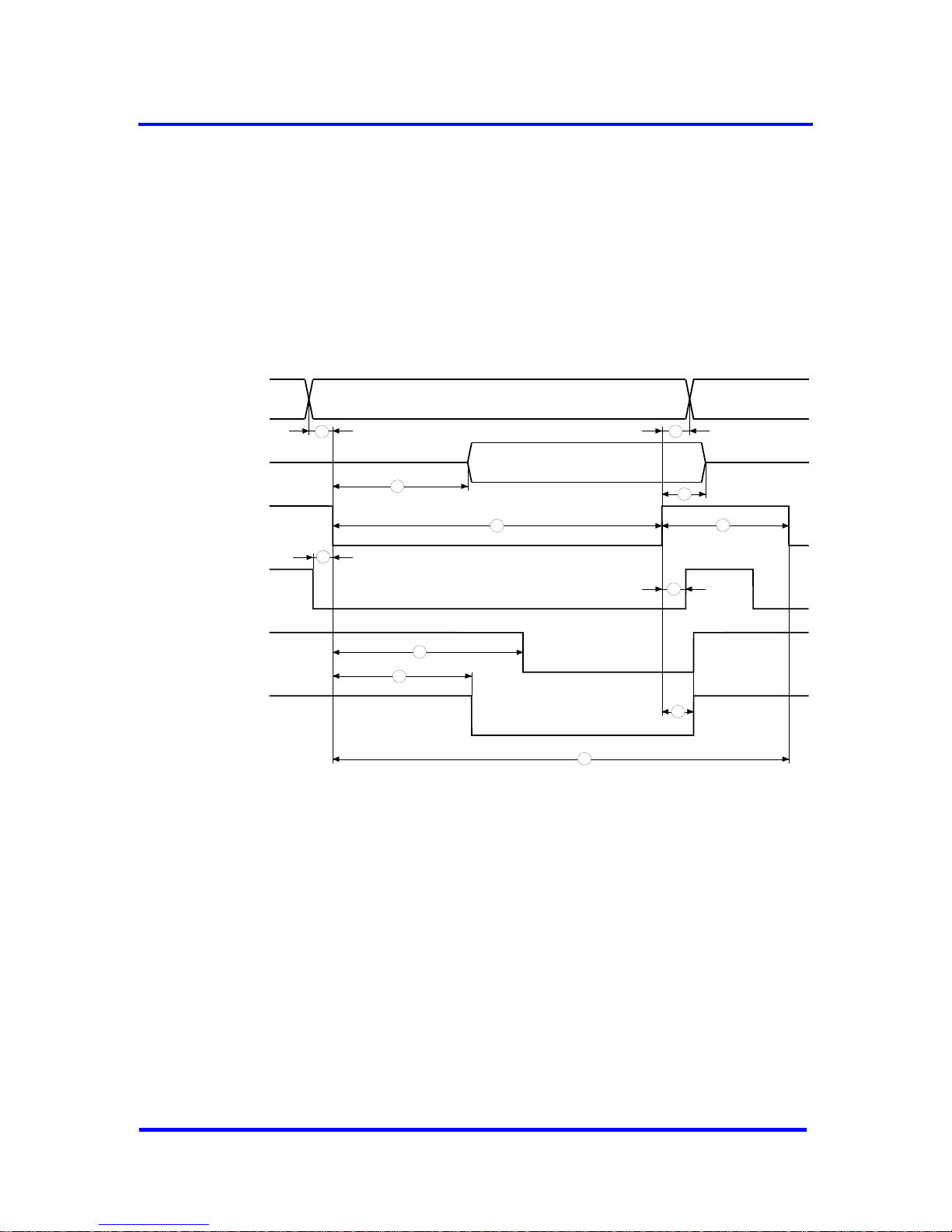
Operational Specifications 10
10.7.3 Timing in the Asynchronous Intel Mode
In the asynchronous Intel mode, the VPC3+C acts like a memory with
ready logic. The access time depends on the type of access. The request
for an access to the VPC3+C is generated from the falling edge of the read
signal (XRD) or the rising edge of the write signal (XWR).
The VPC3+C generates the Ready signal synchronously to the system
clock. The Ready signal gets inactive when the read or the write signal is
deactivated. The data bus is switched to Tristate with XRD = '1'.
AB10..0
DB7..0
XRD
valid
data valid
XCS
X
READY
(normal)
X
READY
(early)
22
27
26
25
24
23
17
16
18
19
20
21
Intel Mode, READ (XWR = 1) Figure 10-12: Asynchronous
VPC3+C User Manual
Revision 1.03 87
Copyright © profichip GmbH 2004-2006
Page 88
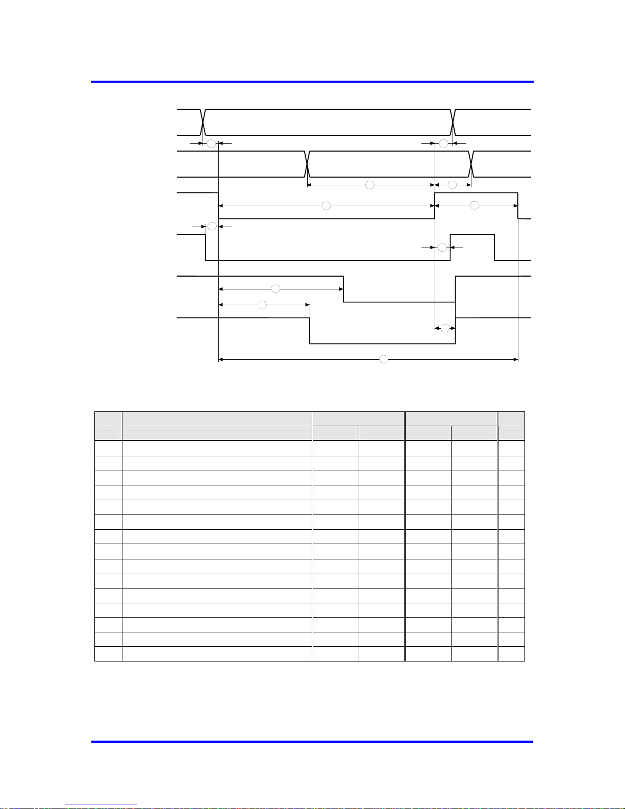
10 Operational Specifications
AB10..0
valid
DB7..0
XWR
XCS
data valid
X
READY
(normal)
X
READY
(early)
22
27
25
30
23
28
16
29
19
26
20
21
Figure 10-13: Asynchronous Intel Mode, WRITE (XRD = 1)
VDD = 3.3 V VDD = 5 V
No. Parameter
MIN MAX MIN MAX
Unit
16
address-setuptime to XRD / XWR ↓
0
0 ns
17
XRD ↓ to data valid
103
97 ns
18 XRD pulsewidth 115 115 ns
19
XCS ↓ setup
0 ns
time to XRD / XWR ↓
0
20
XRD ↓ to XREADY ↓ (Normal-Ready)
132
126 ns
21
XRD ↓ to XREADY ↓ (Early-Ready)
111
105 ns
22 XRD / XWR cycletime 125 125 ns
23
address holdtime after XRD / XWR ↑
0
0 ns
24
data holdtime after XRD ↑
4 16
4 13 ns
25 read/write inactive time 10 10 ns
26
XCS holdtime after XRD / XWR ↑
0
0 ns
27 XREADY holdtime after XRD / XWR 6 21 5 16 ns
28
data setuptime to XWR ↑
10
10 ns
29 XWR pulsewidth 83 83 ns
30
data holdtime after XWR ↑
10
10 ns
Figure 10-14: Timing, Asynchronous Intel Mode
88 Revision 1.03
VPC3+C
User Manual
Copyright © profichip GmbH 2004-2006
Page 89
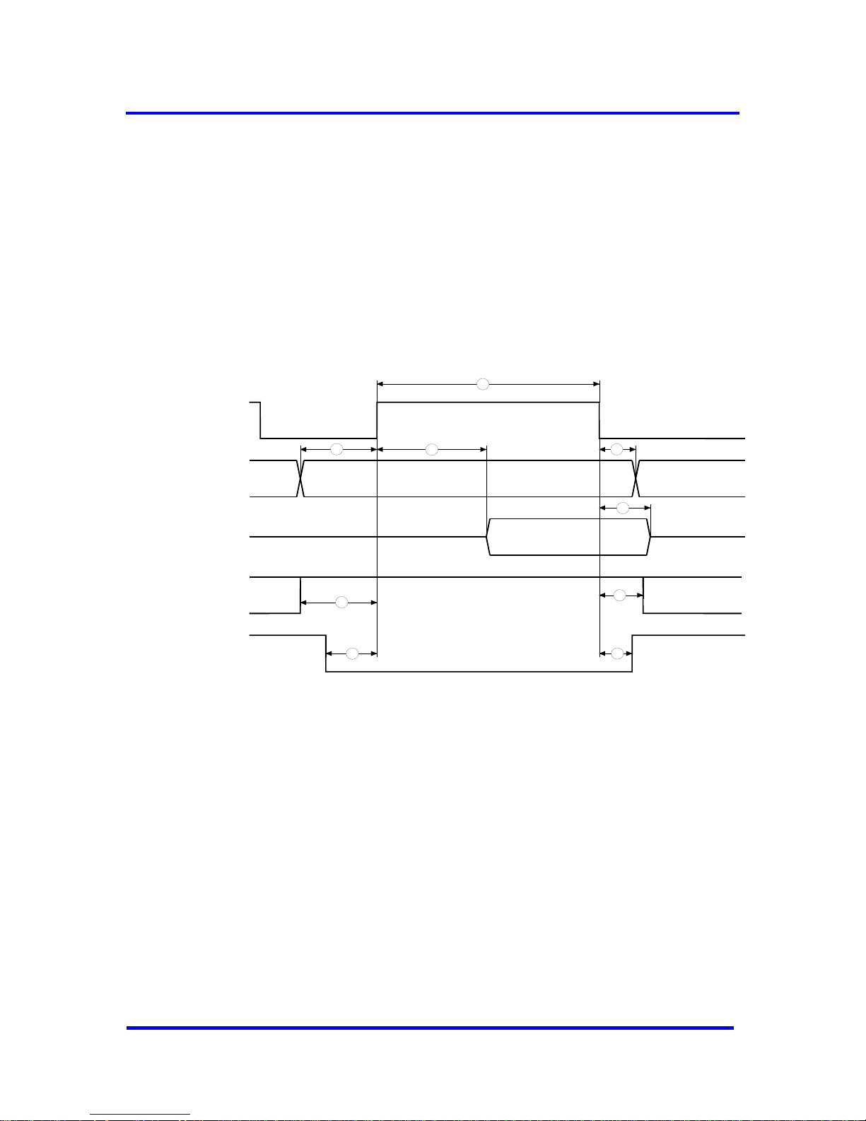
Operational Specifications 10
10.7.4 Timing in the Synchronous Motorola Mode
If the CPU is clocked by the VPC3+C, the output clock pulse (CLKOUT 2/4)
must be 4 times larger than the E_Clock. That is, a clock pulse signal must
be present at the CLK input that is at least 10 times larger than the desired
system clock pulse (E_Clock). The Divider-Pin must be connected to ‘0’
(divider 4). This results in an E_Clock of 3 MHz.
The request for a read access to the VPC3+C is derived from the rising
edge of the E_Clock (in addition: XCS = 0, R_W = 1). The request for a
write access is derived from the falling edge of the E_Clock (in addition:
XCS = 0, R_W = 0).
AB10..0
DB7..0
R_W
valid
lid
E_CLOCK
data va
XCS
35
40
37
39
32
38
33
31
36
chronous Motorola-M de, READ AS = 1) Figure 10-15: Syn o (
VPC3+C User Manual
Revision 1.03 89
Copyright © profichip GmbH 2004-2006
Page 90
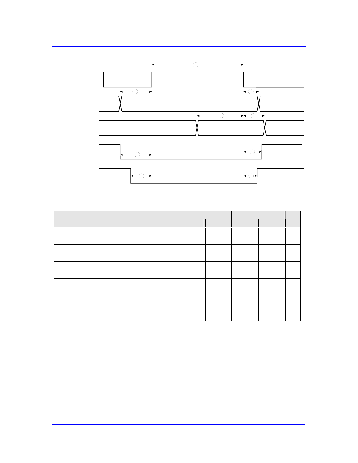
10 Operational Specifications
AB10..0
DB7..0
valid
data valid
XCS
R_W
E_CLOCK
35
40
37
39
42
41
33
31
36
Figure 10-16: Synchronous Motorola-Mode, WRITE (AS = 1)
VDD = 3.3 V VDD = 5 V
No. Parameter
MIN MAX MIN MAX
Unit
31 E_Clock pulse width 136.7 136.7 ns
33
Address setuptime (A10..0) to E_Clock ↑
10
10 ns
37
Address holdtime after E_Clock ↓
5
5 ns
32
E_Clock ↑ to Data valid
103
97 ns
38
Data holdtime after E_Clock ↓
4 16
4 12 ns
35
R_W setuptime to E_Clock ↑
10
10 ns
39
R_W holdtime after E_Clock ↓
5
5 ns
36
XCS setuptime to E_Clock ↑
0
0 ns
40
XCS holdtime after E_Clock ↓
0
0 ns
41
Data setuptime to E_Clock ↓
10
10 ns
42
Data holdtime after E_Clock ↓
10
10 ns
Figure 10-17: Timing, Synchronous Motorola Mode
90 Revision 1.03
VPC3+C
User Manual
Copyright © profichip GmbH 2004-2006
Page 91
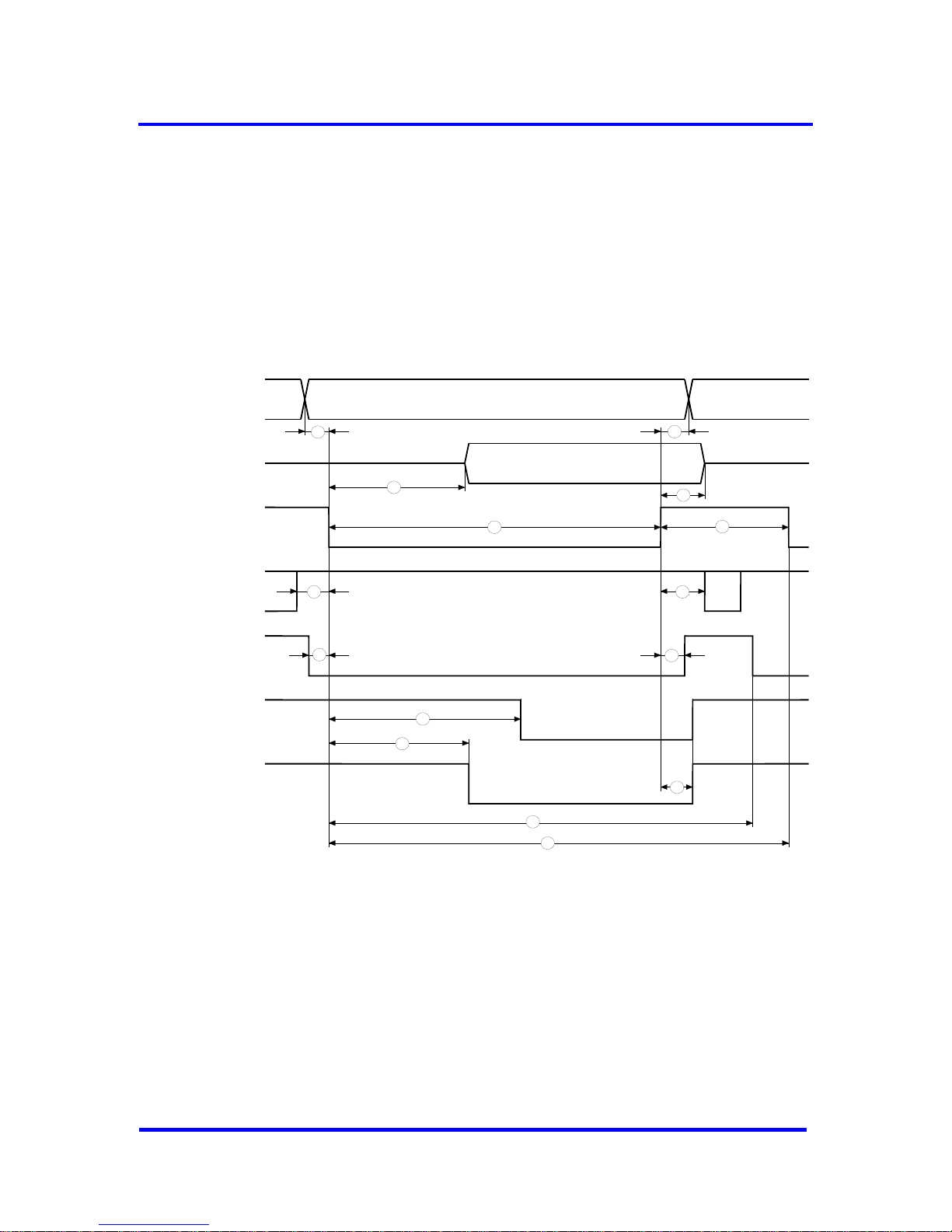
Operational Specifications 10
10.7.5 Timing in the Asynchronous Motorola Mode
In the asynchronous Motorola mode, the VPC3+C acts like a memory with
Ready logic, whereby the access times depend on the type of access.
The request for an access of the VPC3+C is generated from the falling
edge of the AS signal (in addition: XCS = '0', R_W = '1'). The request for a
write access is generated from the rising edge of the AS signal (in addition:
XCS = '0', R_W = '0').
AB10..0
DB7..0
valid
data valid
XCS
X
DTACK
(normal)
X
DTACK
(early)
AS
R_W
56
57
55
54
53
52
44
43
45
46
48
49
47
51
50
Figure 10-18: Asynchronous Motorola Mode, READ (E_CLOCK = 0)
VPC3+C User Manual
Revision 1.03 91
Copyright © profichip GmbH 2004-2006
Page 92
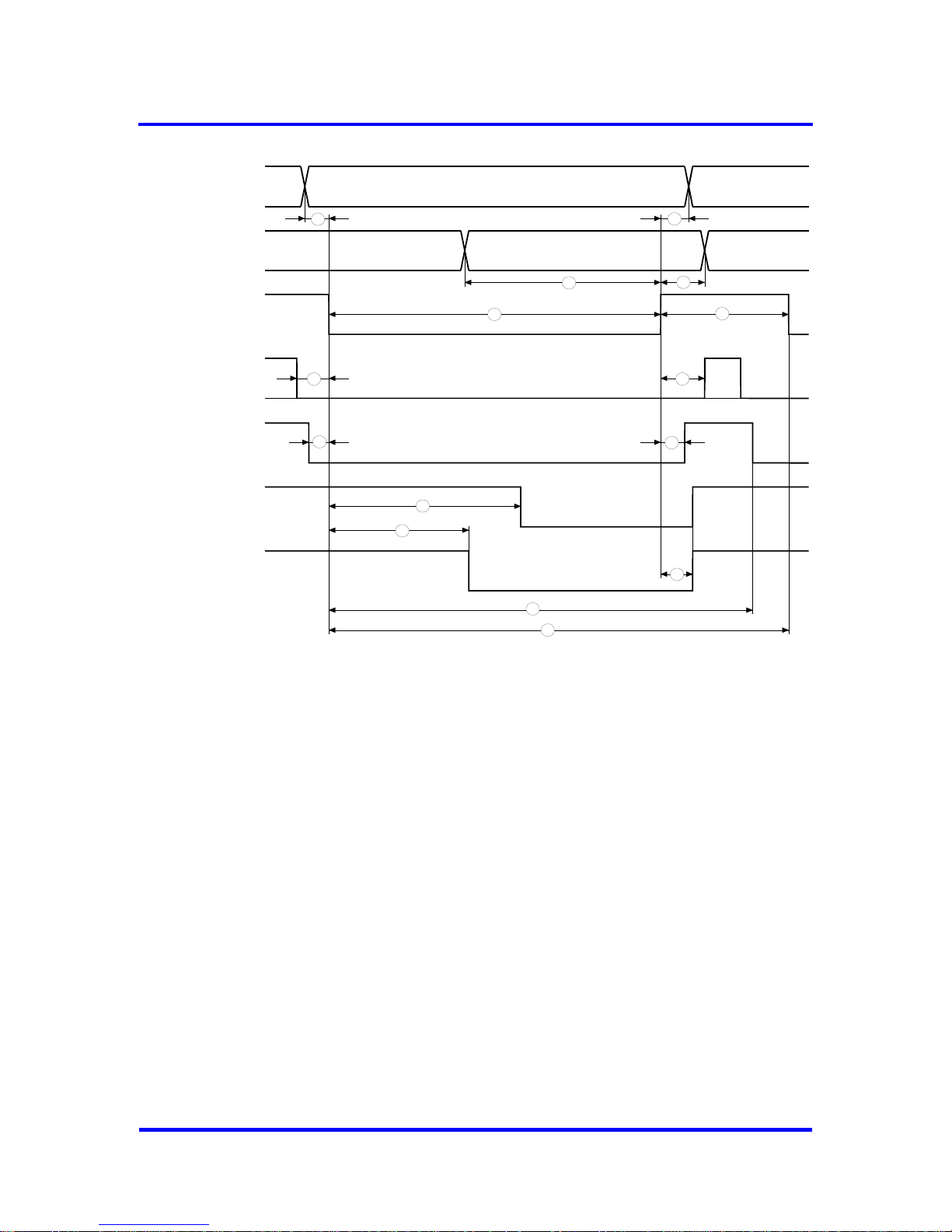
10 Operational Specifications
AB10..0
DB7..0
valid
data alid v
AS
XCS
X
DTACK
(normal)
X
DTACK
(early)
R_W
56
60
57
55
54
52
58
43
59
46
48
49
47
51
50
Figure 10-19: Asynchronous Motorola Mode (WRITE)
92 Revision 1.03
VPC3+C
User Manual
Copyright © profichip GmbH 2004-2006
Page 93
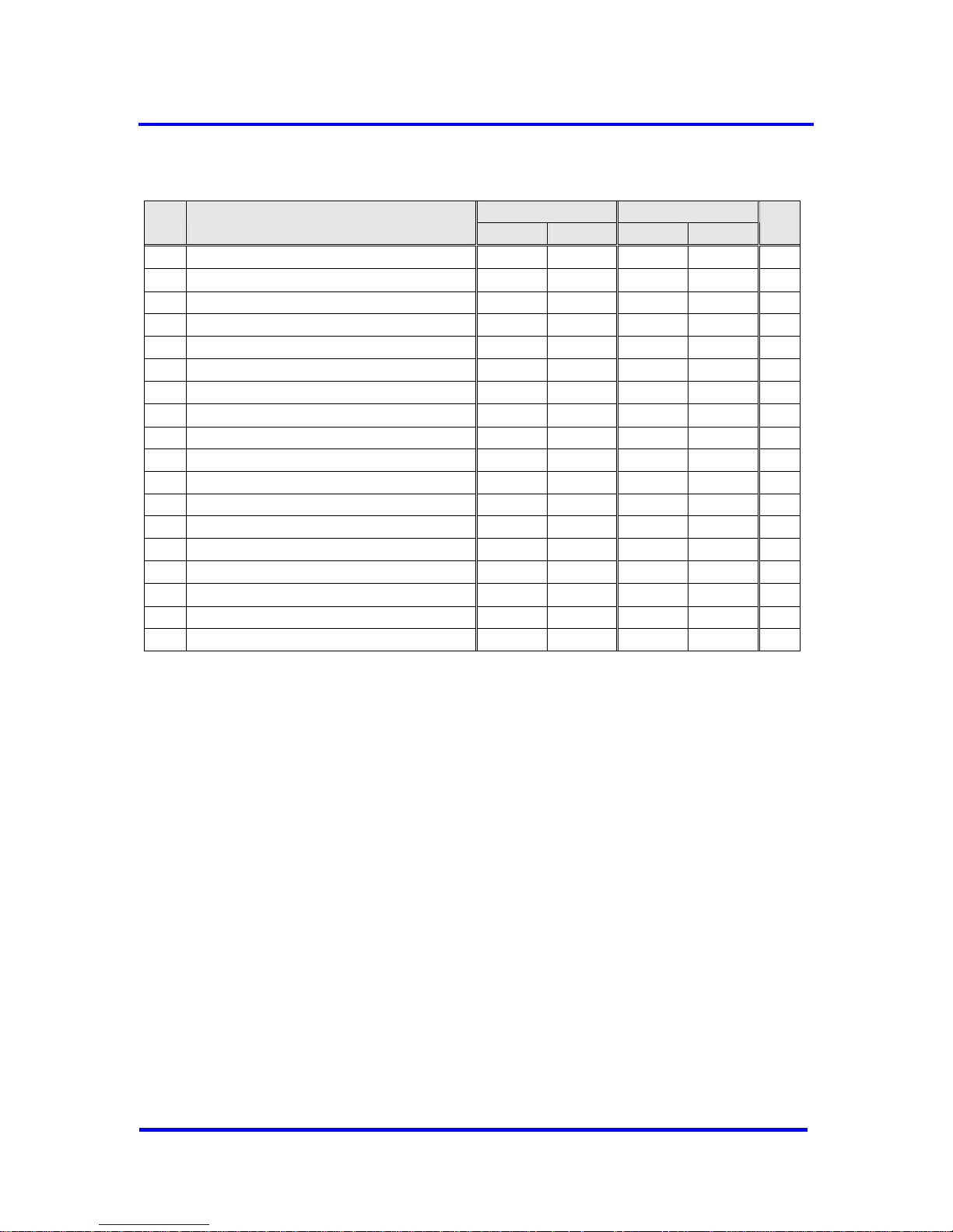
Operational Specifications 10
VDD = 3.3 V VDD = 5 V
No. Parameter
MIN MAX MIN MAX
Unit
43
address setuptime to AS ↓
0
0 ns
44
AS ↓ to data valid
103
97 ns
45 AS pulsewidth (read access) 115 115 ns
46
R_W ↓ setuptime to AS ↓
10
10 ns
47
XCS ↓ setuptime to AS ↓
5
5 ns
48
AS ↓ to XDTACK ↓ (Normal-Ready)
132
126 ns
49
AS ↓ to XDTACK ↓ (Early-Ready)
111
105 ns
50
last AS ↓ to XCS ↓
93
93 ns
51 AS cycletime 125 125 ns
52
address holdtime after AS ↑
10
10 ns
53
Data holdtime after AS ↑
4 16
4 13 ns
54 AS inactive time 10 10 ns
55
R_W holdtime after AS ↑
10
10 ns
56
XCS holdtime after AS ↑
0
0 ns
57
XDTACK holdtime after AS ↑
6 21
5 16 ns
58
Data setuptime to AS ↑
10
10 ns
59 AS pulsewidth (write access) 83 83 ns
60
Data holdtime after AS ↑
10
10 ns
Figure 10-20: Timing, Asynchronous Motorola Mode
VPC3+C User Manual
Revision 1.03 93
Copyright © profichip GmbH 2004-2006
Page 94
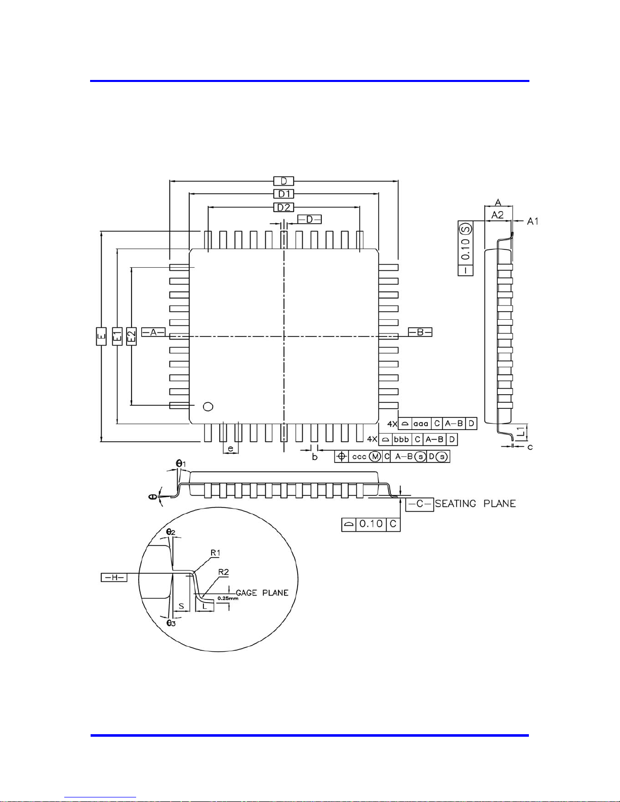
10 Operational Specifications
10.8 Package
Figure 10-21: Package Drawing
94 Revision 1.03
VPC3+C
User Manual
Copyright © profichip GmbH 2004-2006
Page 95
Operational Specifications 10
MILLIMETER INCH
SYMBOL
MIN NOM MAX MIN NOM MAX
A ─── ─── 2.45 ─── ─── 0.096
A1 0.15 0.25 0.35 0.006 0.010 0.014
A2 1.95 2.05 2.10 0.077 0.081 0.083
D 13.90 BASIC 0.547 BASIC
D1 10.00 BASIC 0.394 BASIC
E 13.90 BASIC 0.547 BASIC
E1 10.00 BASIC 0.394 BASIC
R2 0.13 ─── 0.30 0.005 ─── 0.012
R1 0.13 ─── ─── 0.005 ─── ───
Θ 0° 3.5° 7° 0° 3.5° 7°
Θ1 0° ─── ─── 0° ─── ───
Θ2 10° REF 10° REF
Θ3 7° REF 7° REF
c 0.11 0.15 0.23 0.004 0.006 0.009
L 0.73 0.88 1.03 0.029 0.035 0.041
L1 1.95 REF 0.077 REF
S 0.40 ─── ─── 0.016 ─── ───
b 0.22 0.30 0.38 0.009 0.012 0.015
e 0.80 BSC. 0.031 BSC.
D2 8.0 0.315
E2 8.0 0.315
Tolerances of Form and Position
aaa 0.25 0.010
bbb 0.20 0.008
ccc 0.20 0.008
Figure 10-22 : Package Dimensions and Tolerances
Notes:
1. Dimensions D1 and E1 do not include mold protrusion. Allowable
protrusion is 0.25 mm per side. Dimensions D1 and E1 do not
include mold mismatch and are determined at datum plane ─H─.
2. Dimension b does not include dambar protrusion. Allowable dambar
protrusion shall be 0.08 mm total in excess of the b dimension at
maximum material condition. Dambar cannot be located on the
lower radius of the lead foot.
VPC3+C User Manual
Revision 1.03 95
Copyright © profichip GmbH 2004-2006
Page 96

10 Operational Specifications
10.9 Processing Instructions
Generally, ESD protective measures must be maintained for all electronic
components. The VPC3+C is a cracking-endangered component that must
be properly handled.
A drying process must be carried out before the VPC3+C is processed. The
component must be dried for 24 hours at 125°C and then processed within
48 hours. Due to the solderability of the component this drying process may
be carried out once only.
96 Revision 1.03
VPC3+C
User Manual
Copyright © profichip GmbH 2004-2006
Page 97
Revision History
Version Date Page Remarks
V1.00 10.05.2004 First release
V1.01 18.07.2004 Re-formatting and correction of typing errors
V1.02 22.09.2004 Some minor corrections
V1.03 12.01.2006
57
80
85
Consecutive paging
Additional figures for FDL-Interface
Figure 9-2 updated
Figure 10-10 revised
VPC3+C User Manual
Revision 1.03 97
Copyright © profichip GmbH 2004-2006
Page 98

profichip GmbH
Einsteinstrasse 6
91074 Herzogenaurach
Germany
Phone : +49.9132.744-200
Fax: +49.9132.744-204
www.profichip.com
The C lever Alternative
 Loading...