

Version
Comment
0.1
First Draft
0.2
Update pin out description
0.3
Change Operation Temperature to -40 ~ 85℃
0.4
Add FCC Statement
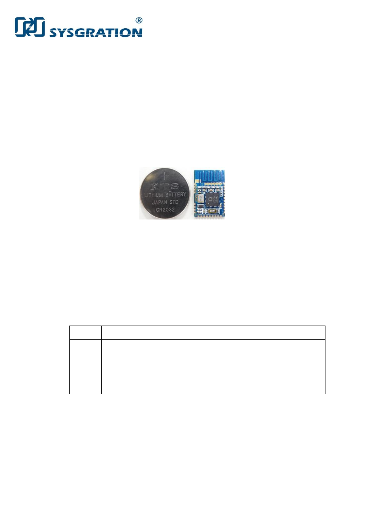
SY-MQ1216X1
SY-MQ1212Y1
SPECIFICATION
▪ DATE OF ISSUE : 2013/12/11
▪ PRODUCT: Bluetooth Low Power Module
▪ MODEL: SY-MQ1216X1(Antenna embedded), SY-MQ1212Y1(None Antenna)
▪ Rev. V.04

SY-MQ12XXX Product Specification Document
2015/2/6
2
1. Key Features
True single-chip BLE SoC solution
• Integrated BLE radio
• Complete BLE protocol stack and application profiles
• Flexible analog/digital sensor interface
• Fast MCU with Flash memory to run applications
• Support both master and slave modes
Microcontroller
• Integrated 32-bitARM Cortex M0 MCU
• 64kB system memory
• User controllable code protection
• External application processor interface
High level integration
• 4-channel 10-bit general purpose ADC
• 2 general purpose analog comparator
• 15 GPIO pins
• GPIO pins can be used as interrupt sources
• Four general purpose timers
• 32-kHz sleep timer
• Watchdog timer
• Real time clock with calibration
• 2-channel programmable PWM
• Two SPI/UART interface
• I2C master/slave interface
• Brown-out Detector
• Battery monitor and temperature sensor
• AES-128 security coprocessor
• 16/32-MHz crystal oscillator
• Low power 32-kHz RC oscillator
• 32.768-kHz crystal oscillator
2. Typical Applications
• Sports & Fitness
• Healthcare & medical
• Remote control
• Smart phone accessories
• PC peripherals (mouse, keyboard)
• Wireless Sensor networks

SY-MQ12XXX Product Specification Document
2015/2/6
3
BLE SoC
QN9021
SPI
Interface
Board Antenna
LC Filter
UART
Interface
I2C
Interface
Crystal
32.768KHz
Crystal
16M/32MHz
DC/DC
Converter
GPIO Pins
3. Hardware Block Diagram
Crystal 16MHz ± 10ppm
Brand: PSE
Model: FH1600038
32.768KHz Crystal ± 20ppm
Brand: Inscore
Model: FC-135-32.768

SY-MQ12XXX Product Specification Document
2015/2/6
4
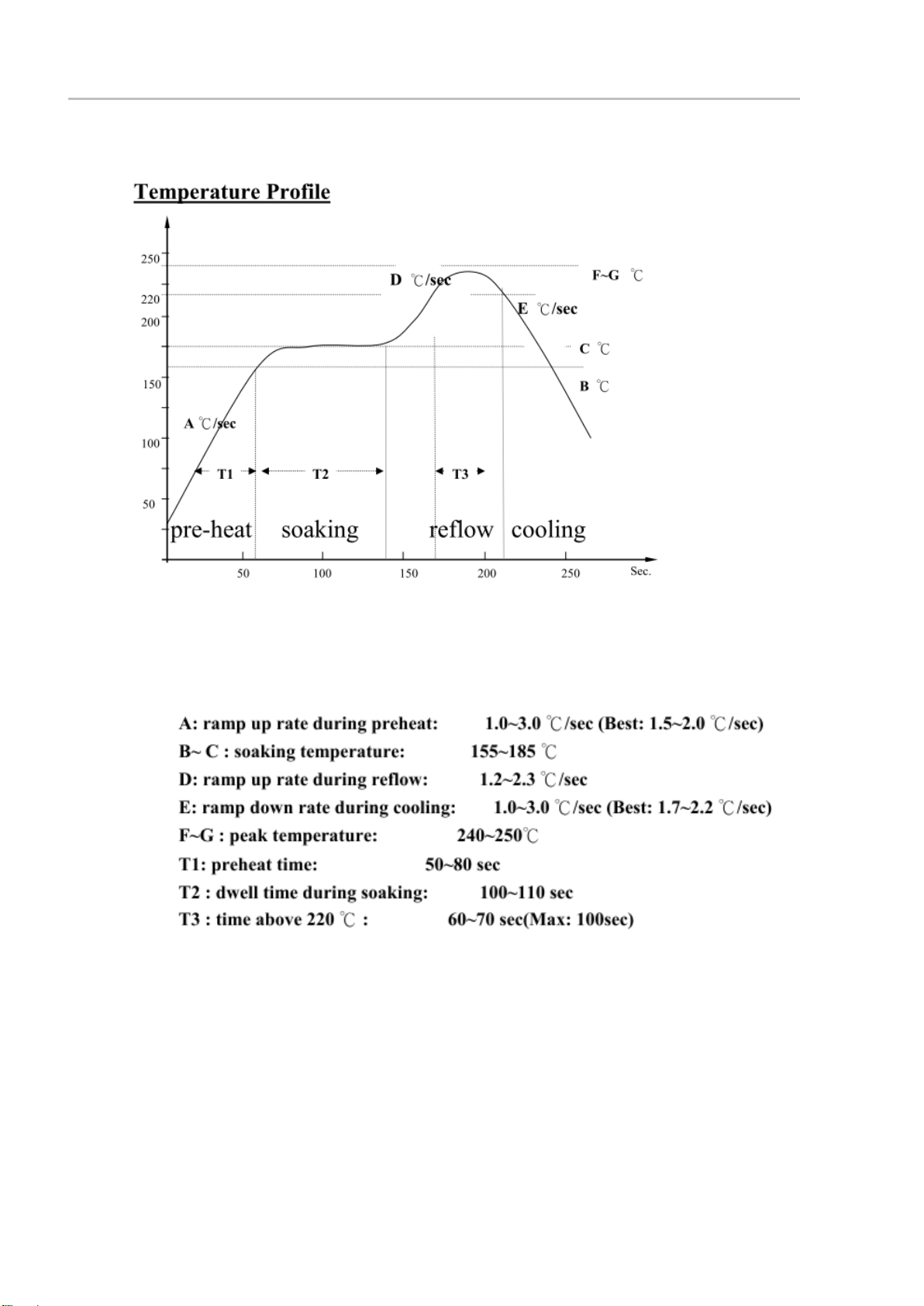
4. Package Mechanical Drawing and Dimension
Top View
Embedded Antenna Version

SY-MQ12XXX Product Specification Document
2015/2/6
5
None Antenna Version

SY-MQ12XXX Product Specification Document
2015/2/6
6
Bottom View
Embedded Antenna Version

SY-MQ12XXX Product Specification Document
2015/2/6
7
None Antenna Version

SY-MQ12XXX Product Specification Document
2015/2/6
8
5. Pin Assignment
Embedded Antenna Version

SY-MQ12XXX Product Specification Document
2015/2/6
9
None Antenna Version

SY-MQ12XXX Product Specification Document
2015/2/6
10
Pins
Name
Function
Description
J1
/RSTN
I
Hardware reset, active low.
J2
P2.3_I2C-SDA
I/O
I2C- Serial Clock. I2C is integrated and support both
master and slave mode. It can communicate with
digital sensor or EEPROM.
J3
P2.4_I2C-SCL
I/O
I2C- Serial Data. I2C is integrated and support both
master and slave mode. It can communicate with
digital sensor or EEPROM.
J4
P2.6_PWM
O
The PWM provides two channel PWM waveforms
with programmable period and duty cycle. It has two
8-bit auto reload down counter and programmable
10-bit prescaler for both channels.
J5
P2.7_PWM
O
The PWM provides two channel PWM waveforms
with programmable period and duty cycle. It has two
8-bit auto reload down counter and programmable
10-bit prescaler for both channels.
J6
P1.0_SPI1-MISO
O
SPI data output
J7
P1.1_SPI1-MOSI
I
SPI data input
J8
P1.2_SPI1-CS
I/O
Chip select for SPI, active low
J9
P1.3_SPI1-CLK
I/O
SPI clock
J10
GND
Ground
Ground
J11
P1.7_UART0-RX
I
The UART supports the Bluetooth Low Energy Direct
Test Mode (DTM).This interface is used to control the
PHY layer with commercially available Bluetooth
testers used for qualification.
J12
P0.0_UART0-TX
O
The UART supports the Bluetooth Low Energy Direct
Test Mode (DTM).This interface is used to control the
PHY layer with commercially available Bluetooth
testers used for qualification.
J13
P0.3_INT0
I
interrupt input
J14
XTAL_32K_OUT
Analog in
32.768KHz installed, Disconnect all to this Pin.
J15
XTAL_32K_IN
Analog In
32.768KHz installed, Disconnect all to this Pin.
J16
SWDIO
I/O
Serial Wire Data Input/Output. The Module provides
a standard Serial Wire Debug (SWD) interface and
supports up to four hardware breakpoints and two
watchpoints.
J17
SWCLK
I
Serial Wire Clock. Module provides a standard Serial
Wire Debug (SWD) interface and supports up to four
hardware breakpoints and two watchpoints.
J18
EXT_VCC
Power
Power Supply
J19
GND
Ground
Ground
J20
VDD_IDC
Power
Internal DC/DC enabled, Disconnect all to this Pin.
J21
P3.0
I/O
The Module integrates a general purpose 8/10-bit
SAR ADC, with up to 50k sampling rate. It includes
an analog multiplexer with up to four external input
channels. Conversion results can be moved to
memory through DMA.
J22
P3.1
I/O
The Module integrates a general purpose 8/10-bit
SAR ADC, with up to 50k sampling rate. It includes
an analog multiplexer with up to four external input
channels. Conversion results can be moved to
memory through DMA.
J23
GND
Ground
Ground
J24
GND
Ground
Ground
J25
GND
Ground
Ground
J26
GND
Ground
Ground
J27
RF
TX/ RX
Antenna Feed Port (Only for None Antenna
version)
6. Pin Assignment Description
SY-MQ12XXX Product Specification Document
2015/2/6
11
SYMBOL
PARAMETER
CONDITIONS
MIN
MAX
UNIT
EXT_VCC
Supply voltage
VCC to GND
-0.3 5 V
Ts
Storage temperature
-55
150
℃
ESD
Human-body model
REN,RFP
1.5
KV
Other pads
2
KV
Machine model
All pads
200
V
Charge-device model
All pads
1000
V
SYMBOL
PARAMETER
CONDITIONS
MIN
TYP
MAX
UNIT
EXT_VCC
Power Supply
Relative to GND
2.4
3.0
3.6 V T A
Operating temperature
-40
+25
+85
℃
Symbol
Conditions
Min.
Typ.
Max.
Unit
Frequency
ISM Band
2400
_
2483.5
MHZ
Output Power
-4 +4
dBm
Tx Power adjust step
2 dB
Modulation
GFSK
Data Rate
On-air data rate
250K
1M
2M
bps
Receive Sensitivity
250Kbps,1Mbps, 1Mbps BLE
-90
-85
dBm
7. Electrical Specifications
Absolute Maximum Ratings
Recommended Operating Conditions
Radio Characteristics

SY-MQ12XXX Product Specification Document
2015/2/6
12
DC Characteristics
The sinking current is about 7.8mA in low driver and about 30mA in high driver
The sourcing current is about 9.5mA in low driver and about 36mA in high driver.

SY-MQ12XXX Product Specification Document
2015/2/6
13
8. System Descriptions
RF transceiver
Radio transceiver is compliant with the Bluetooth v4.0 Low Energy specification Volume 6,
Part A.
Imbedded oscillators
The Module includes two integrated oscillators:
Low power high frequency 16MHz crystal.
Ultra low power 32.768KHz crystal.
The high frequency crystal oscillator provides the reference frequency for the radio
transceiver. The low frequency 32.768KHz oscillators provide the protocol timing.
Supply voltage
The Module includes highly efficient integrated regulators to generate all internal suppl
yvoltages from a single external supply voltage. This is particularly usefulfor application
susing battery technologies with higher nominal cell voltages.
General purpose ADC
The Module integrates a general purpose 8/10-bit SAR ADC, with up to 50k sampling
rate. It includes an analog multiplexer with up to four external input channels.
Conversion results can be moved to memory through DMA.
The main features of the ADC are as follows:
Four single-end input channels, or two differential channels
Reference voltage selectable as internal, external single-ended, AVDD
Interrupt request generation
DMA triggers at end of conversions
Window compare function
Temperature sensor input
Battery measurement capability
The ADC could operates in
Single conversion mode
Continuous conversion mode
Scan mode (automatic switching among external inputs)

SY-MQ12XXX Product Specification Document
2015/2/6
14
Analog comparator
The analog comparator is used to compare the voltage of two analog inputs and
adigital output to indicate the higher input voltage. The positive input is always from
external pin and the negative input can either be one of the selectable internal
references or from external pin.
The analog comparator features for low-power operation and the comparing result
can be used as interrupt source to wake up the system from sleep.
Temperature sensor
A temperature sensor is integrated by connecting a diode to ADC input to measure the
voltage and then the silicon temperature is calculated.
Battery monitor
A battery monitor is integrated by connecting supply voltage (VDD/3) to the ADC input,
which would use the internal regulated reference for the conversion.

SY-MQ12XXX Product Specification Document
2015/2/6
15
Profiles/Services
Version
Device Information Service
1.1
Battery Service
1.0
Blood Pressure Profile
1.0
Find Me Profile
1.0
Glucose Profile
1.0
Heart Rate Profile
1.0
Health Thermometer Profile
1.0
HID over GATT Profile
1.0
Proximity Profile
1.0
Scan Parameter Profile
1.0
Time Profile
1.0
Alert Notification Profile
1.0
Phone Alert Status Profile
1.0
Cycling Speed and Cadence Profile
1.0
Running Speed and Cadence Profile
1.0
9. Profiles and Services
10. MCU Subsystem
The MCU subsystem includes
32-bitARM Cortex-M0 MCU
64-kBsystem memory
Reset generation
Clock and power management unit
Nested Vectored Interrupt Controller (NVIC)
Serial Wire Debug interface (SWD)

SY-MQ12XXX Product Specification Document
2015/2/6
16
0xFFFFFFFF
Reserved
0xEFFFFFFF
MCU private peripherals
0xE0000000
Reserved
0x50013FFF
ADC
0x50010000
Reserved
0x50003FFF
GPIO
0x50000000
Reserved
0x400EFFFF
APB peripherals
0x40000000
Reserved
0x1000FFFF
System memory
0x10000000
ROM
0x00000000
MCU
The CPU core is a 32-bit ARM Cortex-M0 MCU, which offers significant benefits to
application development, including:
Simple, easy-to-use programmers model
Highly efficient ultra-low power operation
Excellent code density
Deterministic, high-performance interrupt handling for 32 external interrupt inputs
The processor is extensively optimized for low power, and delivers exceptional power
efficiency through its efficient instruction set, providing high end processing hardware
including a single-cycle multiplier.
Memory organization
The Module integrates 64KB system memory for application program and data. The
system memory, all registers and external devices are allocated in the same memory
map within 4GB, ranging from 0x00000000 to 0xFFFFFFFF, which is shown in
following Figure. The system memory security is ensured with a user controllable
protection scheme, preventing un-authorized read out.
Memory Address Map

SY-MQ12XXX Product Specification Document
2015/2/6
17
RESET generation
The device has four reset sources. The following events generate a reset:
Forcing RSTN pin low
Power-on reset
Brown-out reset
Watchdog timeout reset
Nested Vectored Interrupt Controller (NVIC)
The Module supports Cortext-M0 built-in Nested Vectored Interrupt Controller (NVIC)
with 24 external interrupt inputs. External interrupt signals connect to the NVIC, and
the NVIC prioritizes the interrupts. Software can set the priority of each interrupt.
The NVIC and Cortex-M0 processor core are closely coupled, providing low-latency
interrupt processing and efficient processing of late arriving interrupts.
Clock and power management
The Module provides flexible clocking scheme to balance between performance and
power. A high frequency crystal oscillator is utilized to provide reference frequency
and system clock, which used 16MHz crystal. The system clock could be 32MHz or
its divided versions.
The 32.768KHz crystal oscillator is used for accurate timing and improved power
consumption.
The Module features ultra low power consumption with two sleep modes,
SLEEP and DEEP SLEEP. After execution of Wait for Interrupt (WFI) instruction, the
MCU stops execution, enters into sleep mode and stops the clock immediately.
If DEEP SLEEP mode is entered, it must wait for external interrupts to wake it up.
Before entering into SLEEP mode, MCU should set the sleep timer correctly and
make the 32KHz clock ready.
Once an interrupt (external interrupt or sleep timer timeout) occurs, the Wakeup
Interrupt Controller (WIC) enables the system clock, takes a number of clock cycles
to wake up MCU and restore the states, before MCU can resume program execution
to process the interrupt.
The power management unit is responsible to control the power states of the whole
module and switch on/off the supply to different parts according to the power state.

SY-MQ12XXX Product Specification Document
2015/2/6
18
MODE
DIGITAL
REGULATOR
32KHz OSC
SLEEP
TIMER
NOTE
Power off
Off
Off
Off
No external power supply
Deep sleep
Off
Off
Off
Wait external interrupt to wake
it up. RAM/register content
retained
Sleep
Off
On
On
Wait for SLEEP TIMER
timeout to wake it up.
RAM/register content retained
Idle
On
On
On
MCU idle
Active
On
On
On
Radio off, MCU on
Radio
On
On
On
Radio on.
Power Matrix
Serial Wire Debug (SWD) interface
The Module provides a standard SWD interface and supports up to four hardware
breakpoints and two watchpoints.

SY-MQ12XXX Product Specification Document
2015/2/6
19
11. Digital Peripherals
TIMER (0/1)
TIMER0/1 are general-purpose 32-bit timer with programmable 10-bit prescaler.
The prescaler source is the system clock, 32KHz clock. The timers have below functions:
Input capture function
Compare function
PWM output
The timer generates maskable interrupts for the events of overflow, compare and capture,
which could be used to trigger MCU or ADC conversions.
TIMER (2/3)
TIMER2/3 are general-purpose 16-bit timer with programmable10-bit prescaler.
The prescaler source could be the system clock or 32KHz clock. The timers have
below functions:
Input capture function
Compare function
PWM output
The timer will generate maskable interrupts for the events of overflow, compare and
capture, which could be used to trigger MCU or ADC conversions.
Real Time Clock (RTC)
The RTC is run off the 32KHz clock and provides real time with calibration,
supporting below functions:
Time and date configuration on the fly
Alarm function for 24-hour and minute
Input capture function with programmable noise canceller
Watchdog Timer (WDT)
The Watchdog timer (WDT) is a 16-bit timer clocked by 32KHz clock. It is intended as a
recovery method in situations where the CPU may be subjected to software upset.
The WDT resets the system when software fails to clear the WDT within the selected time
interval. The WDT is configured as either a Watchdog Timer or as a timer for generalpurpose use. If the watchdog function is not needed in an application, it is possible to
configure the Watchdog Timer to be used as an interval timer that can be used to generate
interrupts at selected time intervals. The maximum timeout interval is 1.5 days.

SY-MQ12XXX Product Specification Document
2015/2/6
20
Sleep Timer
The sleep timer is a 32-bit timer running at 32KHz clock rate. It is in always
on power domain, being used to set the interval for system to exit Sleep mode and wakeup
MCU.
PWM
The PWM provides two channel PWM waveforms with programmable period and duty
cycle. It has two 8-bit auto reload down counter and programmable 10-bit prescaler for both
channels. It supports below functions
Predictable PWM initial output state
Buffered compare register and polarity register to ensure correct PWM output
Programmable overflow interrupt generation
DMA
The DMA controller is used to relieve MCU of handling data transfer operations to achieve
high performance and efficiency. It has a single DMA channel to support fixed and
undefined length transfer. The source address and destination address are programmable.
It can be aborted immediately in a transfer process by configuring ABORT register, and
a DMA done interrupt is generated meanwhile.
Random number generator
The Module integrates a random number generator for security purpose.
AES coprocessor
The Advanced Encryption Standard (AES) coprocessor allows encryption/decryption to
be performed with minimal CPU usage. The coprocessor supports 128-bit key and
DMA transfer trigger capability.

SY-MQ12XXX Product Specification Document
2015/2/6
21
12. Communication Interfaces
UART 0/1
The two UARTs have identical function and include the following features:
8-bit payload mode: 8-bit data without parity
9-bit payload mode: 8-bit data plus parity
The parity in 9-bit mode is odd or even configurable
Configurable start- and stop- bit levels
Configurable LSB- or MSB-first data transfer
Parity and framing error status
Configurable hardware flow control
Support overrun
Flexible baud rate: 1.2/2.4/4.8/9.6/14.4/19.2/28.8/38.4/57.6/76.8/115.2/230.4 kbps
SPI 0/1
The two SPIs have identical function and include the following features:
Master/slave mode configurable
4-wire or 3-wire configurable
Clock speed configurable for master mode (divided from 16/32MHz)
4MHz max. clock speed in slave mode
16MHz max. clock speed in master mode
Configurable clock polarity and phase
Configurable LSB or MSB first transfer
I2C
The I2C module provides an interface between the device and I2C-compatible device
sconnected by the two-wire I2C serial bus. The I2C module features include:
Compliance with the I2C specification v2.1
7-bit device addressing modes
Standard mode up to 100 kbps and fast mode up to 400 kbps support
Support master arbitration in master mode
Support line stretch in slave mode

SY-MQ12XXX Product Specification Document
2015/2/6
22
GND
13. Layout Guide
Place the module as close as the mother board edge.
Never place ground plane or tracks underneath the antenna area.
Never place the antenna very close to metallic objects.
Layout for high performance
Locate the antenna as far away as possible from the user’s body.
Do not put the antenna inside a metal enclosure or metalized plastic casing.
Use a 50 ohm track for RF transmission line ( for none Antenna Module)
Uses the ground plane on RF transmission side ( for none Antenna Module)
Better power routing
Components with high current draw must have its own track to the power supply.
Decupling capacitors must be placed as close as possible to power supply pin.
Decupling capacitors must Local ground plane with several vias.
Decoupling capacitors close to noisy components
Make sure all ground planes are connected with lots of vias.
Ground plane between I/O-tracks.
Low impedance ground plane.
Refer the recommend solder pads dimension page and for correct layout procession.
SY-MQ12XXX Product Specification Document
2015/2/6
23
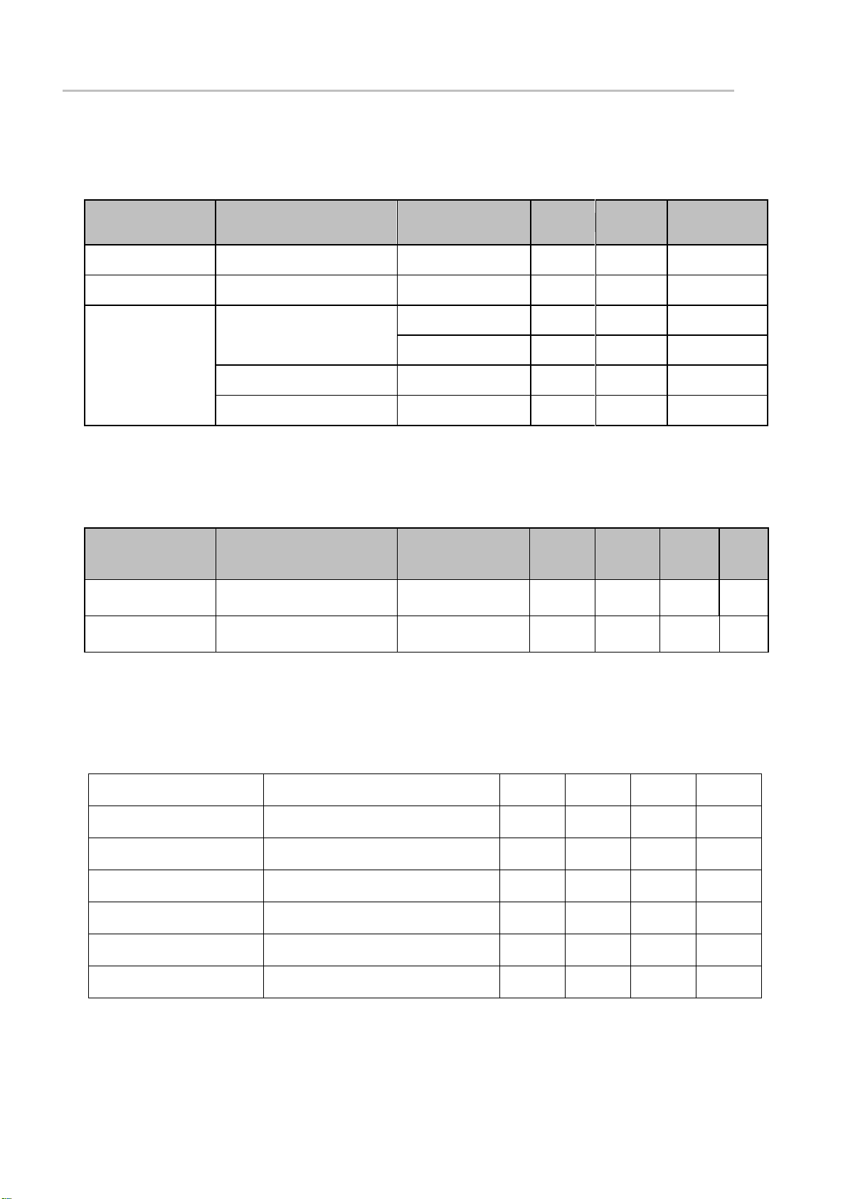
14. Soldering profile

SY-MQ12XXX Product Specification Document
2015/2/6
24
U1
SY-MQ1216X1
P3.1_ADC+
J22
P3.0_ADC-
J21
VDD_IDC
J20
GND
J19
GND
J24
GND
J23
GND
J26
GND
J25
/RSTN
J1
P2.3_I2C_SDA
J2
P2.4_I2C_SCL
J3
P1.0_SPI1_MISO
J6
P1.1_SPI1_MOSI
J7
P1.2_SPI1_CS
J8
P1.3_SPI1_CLK
J9
GND
J10
P1.7_UART0_RX
J11
P0.0_UART0_TX
J12
P0.3_INT0
J13
XTAL_32K_OUT
J14
XTAL_32K_IN
J15
SWDIO
J16
SWCLK
J17
EXT_VCC
J18
P2.6_PWM1
J4
P2.7_PWM2
J5
UART-RX
UART-TX
Application
MCU
VCC
GND
LDO
or
Coil
Battery
VCC
GND
SWCLK
SWDIO
C1
1uF
GND
Reset
2.4V ~ 3.6V
15. Reference Schematic
Embedded Antenna

SY-MQ12XXX Product Specification Document
2015/2/6
25
U1
SY-MQ1212Y1
P3.1_ADC+
J22
P3.0_ADC-
J21
VDD_IDC
J20
GND
J19
GND
J24
GND
J23
GND
J26
GND
J25
/RSTN
J1
P2.3_I2C_SDA
J2
P2.4_I2C_SCL
J3
P1.0_SPI1_MISO
J6
P1.1_SPI1_MOSI
J7
P1.2_SPI1_CS
J8
P1.3_SPI1_CLK
J9
GND
J10
P1.7_UART0_RX
J11
P0.0_UART0_TX
J12
P0.3_INT0
J13
XTAL_32K_OUT
J14
XTAL_32K_IN
J15
SWDIO
J16
SWCLK
J17
EXT_VCC
J18
P2.6_PWM1
J4
RF
J27
P2.7_PWM2
J5
UART-RX
UART-TX
Application
MCU
VCC
GND
LDO
or
Coil
Battery
VCC
GND
SWCLK
SWDIO
C1
1uF
GND
Reset
2.4V ~ 3.6V
L1
C2
E1
N/A
External matching
circuit
None Antenna

SY-MQ12XXX Product Specification Document
2015/2/6
26
16. Recommended of PCB Layout Pads
Embedded Antenna Version
SY-MQ12XXX Product Specification Document
2015/2/6
27
None Antenna Version

SY-MQ12XXX Product Specification Document
2015/2/6
28
17. Contact Information
Sysgration Ltd.(Taiwan)
6Fl., No.1,Sec.1, Tiding Blvd.,
Neihu Dist., Taipei City 11494,
TEL: +886-2-2790-0088
FAX: +886-2-2790-9000
www.sysgration.com
18. Federal Communications Commission (FCC) Statement
15.21
You are cautioned that changes or modifications not expressly approved by the part responsible for
compliance could void the user’s authority to operate the equipment.
15.105(b)
This equipment has been tested and found to comply with the limits for a Class B digital device, pursuant to
part 15 of the FCC rules. These limits are designed to provide reasonable protection against harmful
interference in a residential installation. This equipment generates, uses and can radiate radio frequency
energy and, if not installed and used in accordance with the instructions, may cause harmful interference to
radio communications. However, there is no guarantee that interference will not occur in a particular
installation. If this equipment does cause harmful interference to radio or television reception, which can be
determined by turning the equipment off and on, the user is encouraged to try to correct the interference by
one or more of the following measures:
-Reorient or relocate the receiving antenna.
-Increase the separation between the equipment and receiver.
-Connect the equipment into an outlet on a circuit different from that to which the receiver is connected.
-Consult the dealer or an experienced radio/TV technician for help.
This device complies with Part 15 of the FCC Rules.Operation is subject to the following two conditions:
1) this device may not cause harmful interference and
2) this device must accept any interference received, including interference that may cause undesired operat
ion of the device.
FCC RF Radiation Exposure Statement:
This equipment complies with FCC radiation exposure limits set forth for an uncontrolled environment. End
users must follow the specific operating instructions for satisfying RF exposure compliance. This transmitte
r must not be co-located or operating in conjunction with any other antenna or transmitter.
SY-MQ12XXX Product Specification Document
2015/2/6
29
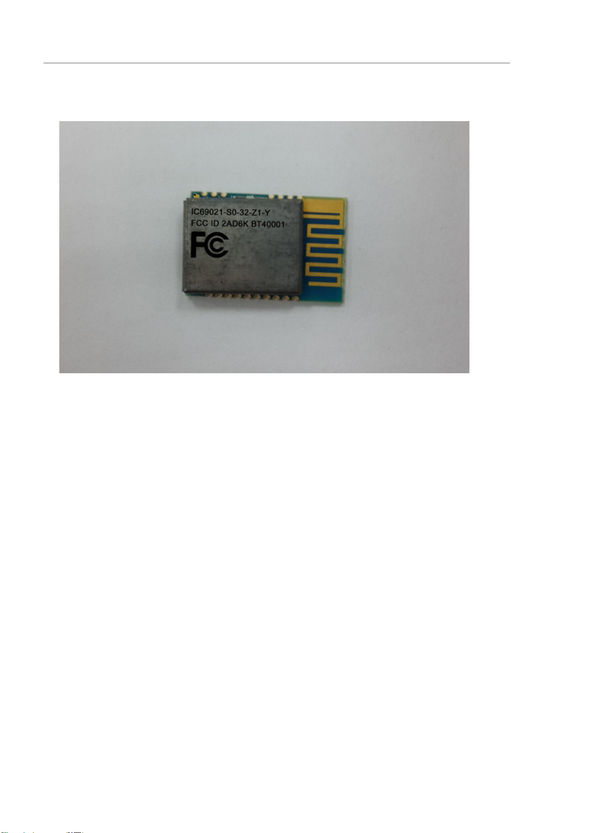
19. Label Drawing
 Loading...