

Page 1
Preliminary PT5622
开关调光专用芯片
简述
PT5622 是一款电子镇流器专用控制芯片,适用于普
通开关的调光产品。它采用灯电流负反馈闭环控制,
提供可编程预热时间与预热频率,其启动电流小,有
精确的振荡频率,应用简单。可提供 DIP16/SOP16
两种封装。
应用范围
• 适合各种型号的荧光灯/CFL 的电子镇流器
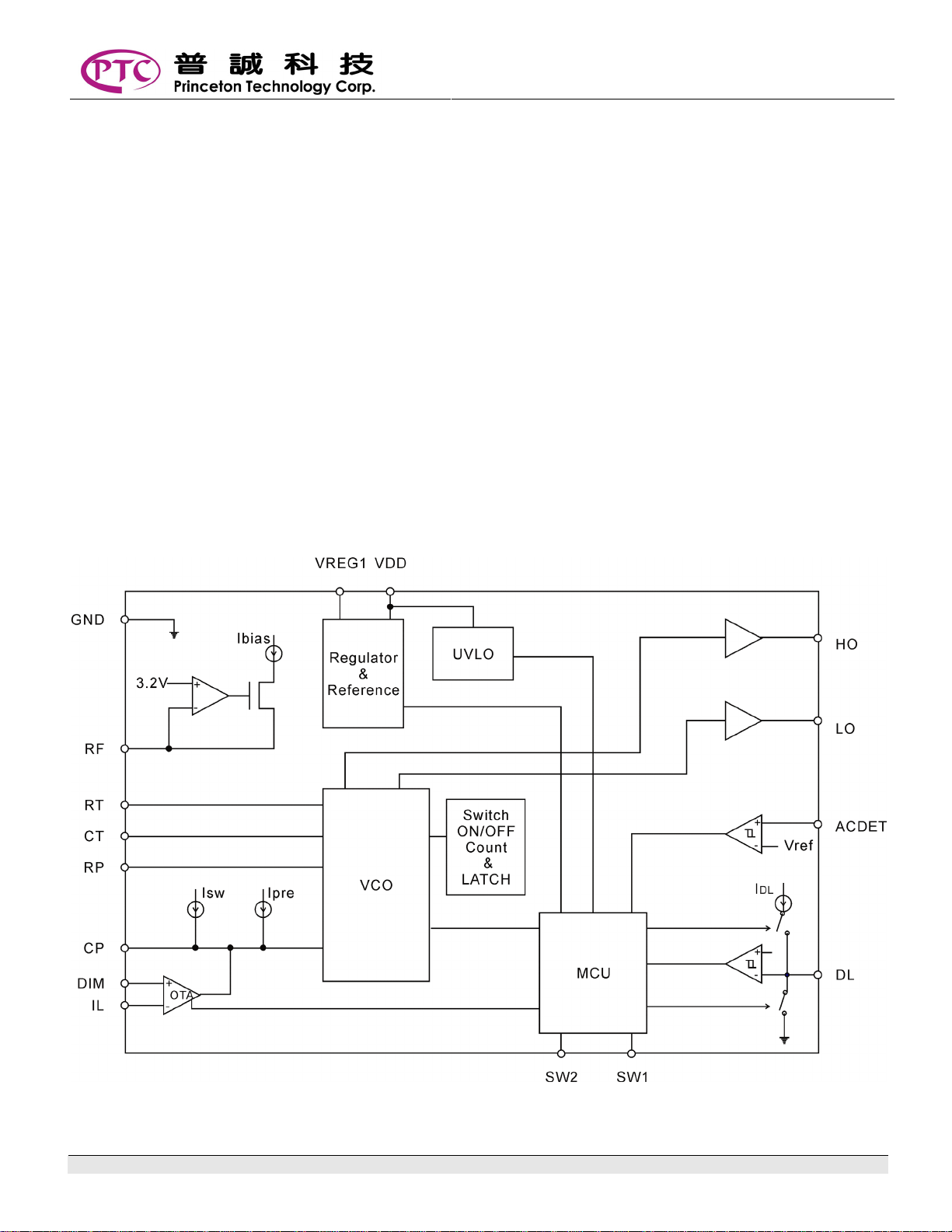
内部电路功能框图
特色
• 普通开关调光电子镇流器专用芯片
• 内部集成 MCU
• 灯电流负反馈控制, 支持低亮度点火
• 可以选择三段或两段、低亮到高亮或高亮到低亮调
光方式
• 可编程预热时间
• 可编程预热频率,扫频点火
• 可编程从开关断开到状态重置延迟时间
• 可编程从开关闭合到进入预热模式的延迟时间
• 固定死区时间
• 提供 DIP16/SOP16 的封装
Tel: 886-66296288‧Fax: 886-29174598‧ http://www.princeton.com.tw‧2F, 233-1, Baociao Road, Sindian, Taipei 23145, Taiwan
Page 2
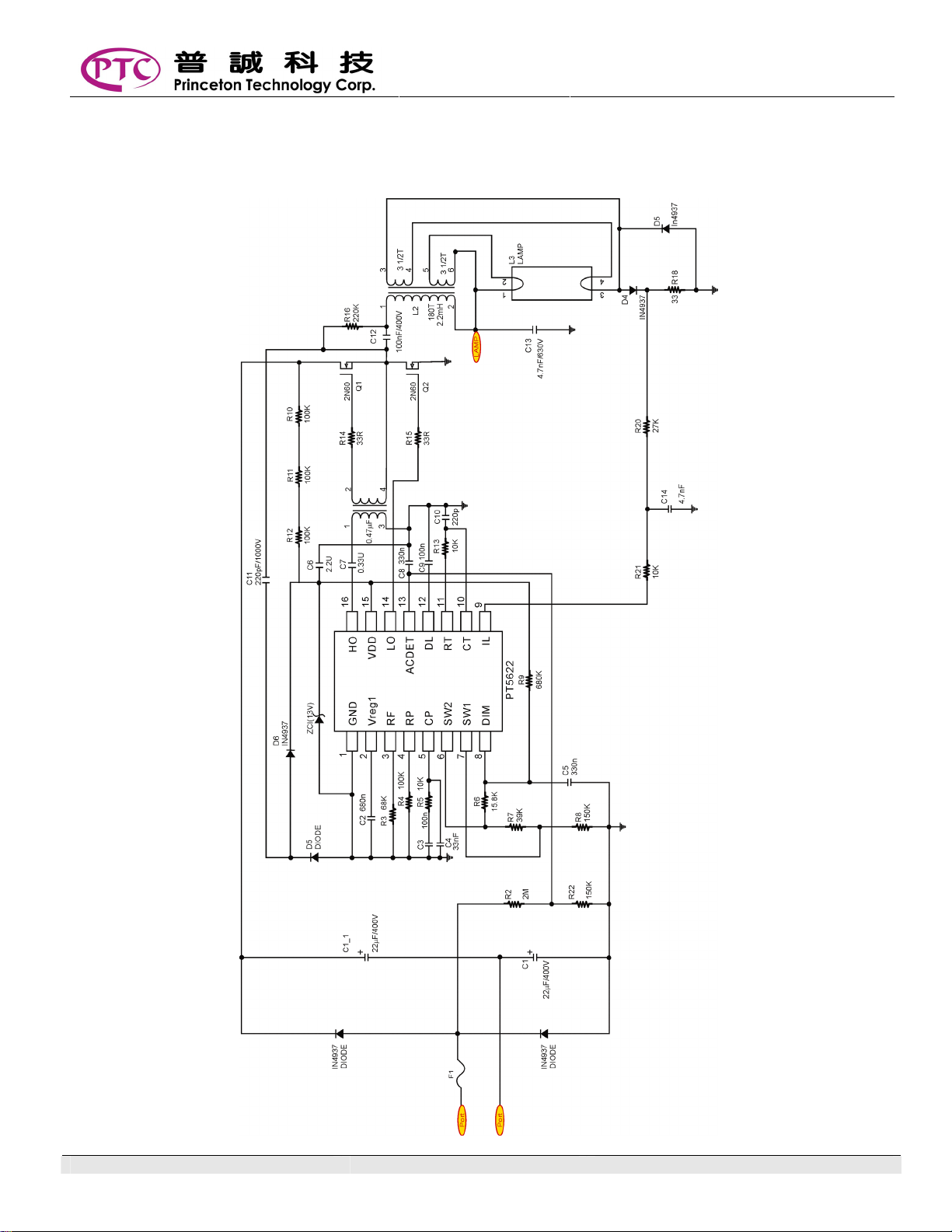
典型应用
PT5622
AC:120V,
输出灯功率
15W/7W/3W
PRE1.0 2 of 14
Page 3
訂購資訊
定购編號 包裝型式 正印
PT5622-D (L) 16 Pins, DIP, 300MIL PT5622-D
PT5622-S (L) 16 Pins, SOP, 150MIL PT5622-S
Notes:
1. (L), (C) or (S) = Lead Free.
2. The Lead Free mark is placed in-front of the date code.
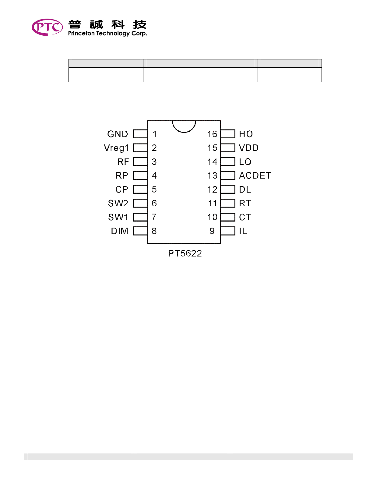
脚位配置图
PT5622
PRE1.0 3 of 14
Page 4
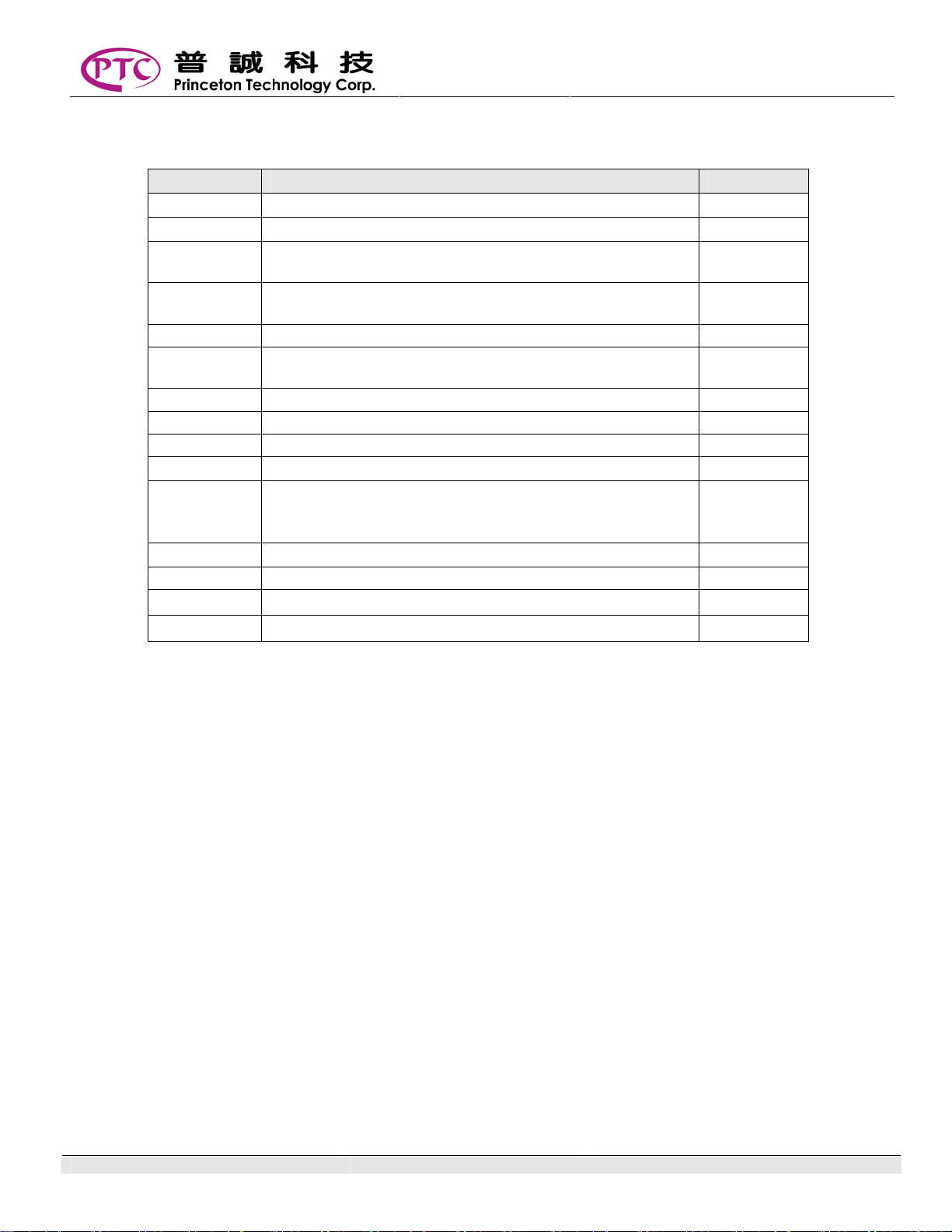
引脚说明
引脚名称 说明 引脚序号
SW2, SW1
ACDET
GND
Vreg1
RF
RP
CP
DIM
IL
CT
RT
DL
LO
VDD
HO
芯片的系统地
芯片备用电源,AC 断开时作为内部 MCU 的供电电源
参考电流设定端。该管脚参考电压恒定为 3.2V,外接电阻生成
内部参考电流源,外接电阻典型值为 68K
预热频率设定端,此管脚输出 30µA 的电流,外接电阻产生一
个电压送入 VCO
预热时间、扫频点火设定端
三段调光设定端。不同的 SW2、SW1 状态改变了外部电阻分
压器的输出电压,而这个电压被作为调光端 DIM 的输入
调光输入端,接收外部电阻分压器的输出电压
灯电流探测端
振荡器外接电容,决定振荡器的频率
振荡器外接电阻,决定振荡器的频率
开关延迟时间设定端,外接电容。当 ACDET 探测到有 AC 输
入时,此管脚输出 1µA 的电流对外接电容充电。在电容电压达
到 3.8V 前,如果 AC 输入没有被切断,则进入预热阶段
AC 输入探测端,用来探测 AC 输入的开关状态及次数
低端功率 MOS 管栅极驱动
芯片的电源端,正常的工作电压为 13V
高端功率 MOS 管栅极驱动
PT5622
1
2
3
4
5
6, 7
8
9
10
11
12
13
14
15
16
PRE1.0 4 of 14
Page 5
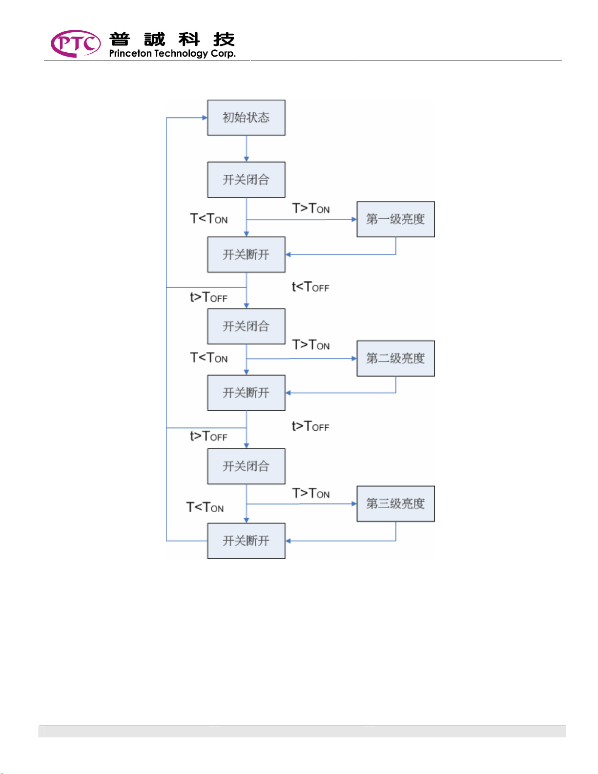
工作逻辑
PT5622
PRE1.0 5 of 14
Page 6
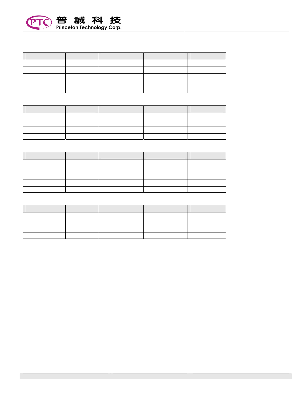
调光说明
PT5622
NO.
PT5622-001
………… …………… ………… ……
表 1: PT5622-001(从高亮到低亮/三段)SW1 与 SW2 逻辑图
NO.
PT5622-002
………… …………… ………… ……
表 2: PT5622-002(从高亮到低亮/两段)SW1 与 SW2 逻辑图
NO.
PT5622-003
………… …………… ………… ……
表 3: PT5622-003(从低亮到高亮/三段)SW1 与 SW2 逻辑图
NO.
PT5622-004
………… …………… ………… ……
表 4: PT5622-004(从低亮到高亮/两段)SW1 与 SW2 逻辑图
开关状态
初始上电
开关一次
开关两次
开关三次
开关状态
初始上电
开关一次
开关两次
开关状态
初始上电
开关一次
开关两次
开关三次
开关状态
初始上电
开关一次
开关两次
SW1 SW2
Floating Floating
Floating GND
GND GND
Floating Floating
SW1 SW2
Floating Floating
GND GND
Floating Floating
SW1 SW2
GND GND
Floating GND
Floating Floating
GND GND
SW1 SW2
GND GND
Floating Floating
GND GND
亮度状态
最亮
中间亮度
最暗
最亮
亮度状态
最亮
最暗
最亮
亮度状态
最暗
中间亮度
最亮
最暗
亮度状态
最暗
最亮
最暗
PRE1.0 6 of 14
Page 7
PT5622
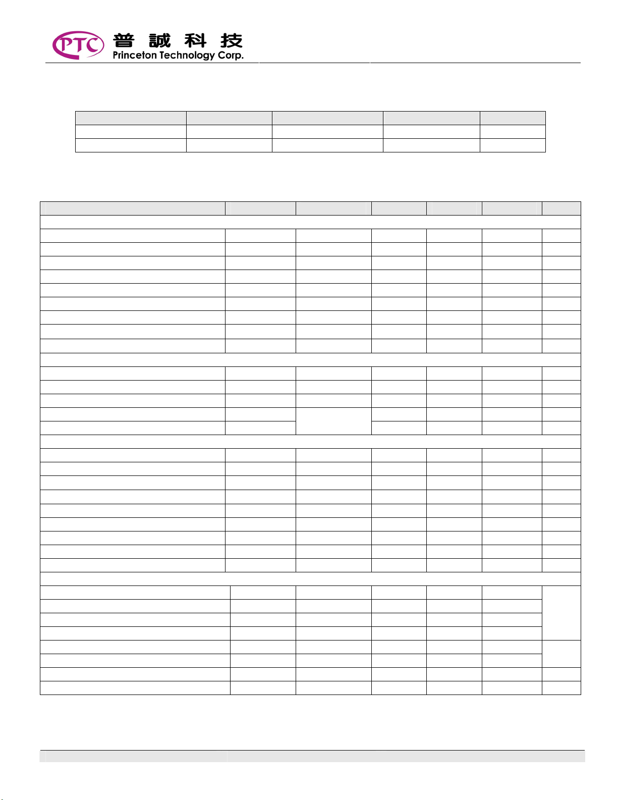
极限值范围
超过给出的极限参数有可能损坏器件或者造成异常工作。所有电压参考系统地。
最小值 最大值
工作温度
贮存温度
参数 符号
Topr -40 +85
Tstg -65 +150
电气特性参数
VDD=13V,RF=68K,ROSC=10K,COSC=330P,Tamb=25℃
参数 符号
供电特性
VDD 欠压锁定之开启电压
VDD 欠压锁定之关闭电压
欠压锁定之滞回电压
欠压锁定时静态电流
VDD 在最大频率下工作时电流
VDD 在最小频率下工作时电流
VDD 内部箝位电压
备用电源 VREG1 欠压锁定之开启电压
备用电源 VREG1 欠压锁定之关闭电压
参考源
内部 Bandgap 电压
上电至 Vref 正常输出时 VDD 电压
VREG1 输出电压
RF 输出电压
RP 输出电流
振荡器输入输出特性
最小振荡频率
振荡器占空比
LO 下降沿到 HO 上升沿的延时
HO 下降沿到LO 上升沿的延时
预热时 CP 充电电流
扫频时 CP 充电电流
CP 最大工作电压
扫频段 CP 电压
点火点电压
驱动级输出特性
在 LO 输出“LOW”时,LO 电压
在 HO 输出“LOW”时,HO 电压
在 LO 输出“HIGH”时,LO 电压
在 HO 输出“HIGH”时,HO 电压
上升延时
下降延时
输出级上拉电流
输出级下拉电流
V
DDUV+ 10.3 10.8 11.3 V
V
DDUV- 8.3 8.8 9.3 V
V
UVHYS - 2 - V
I
QDDUV VDD=10V - 250 350
I
DDHF VCP=0V - 1.0 2 mA
I
DDLF VCP=5V - 0.8 1.2 V
V
CLAMP 15 16 17 V
RG1UV+ - 3.3 - V
V
RG1UV- - 2.7 - V
V
Vref
- 1.25 - V
V
DD-vref 4.9 5 5.5 V
Vregl 5 V
V
RF 3.2 V
I
RP
F
min VCP=5V 32 34 36 KHz
D - 50 - %
LO 1.8 2 2.2
DT
HO 1.8 2 2.2
DT
I
CP_PRE 0.8 1.3 1.8
I
CP_SW 5 6 7
V
CP_MAX 4.9 5 - V
V
CP_SW VRP - 3.8 V
V
CP_run 3.7 3.8 3.9 V
V
LO=LOW - 0 0.1
V
HO=LOW - 0 0.1
V
LO=HIGH VDD-0.1 VDD -
V
HO=HIGH VDD-0.1 VDD -
T
RISE CL=1nF 120 150 170
T
FALL CL=1nF 60 75 90
IO+ 100 140 - mA
IO- 190 230 - mA
测试条件 最小值 典型值 最大值 单位
V
ACDET=5V,
DL=5V
V
单位
℃
℃
30
µA
µA
µs
µA
µA
V
ns
PRE1.0 7 of 14
Page 8
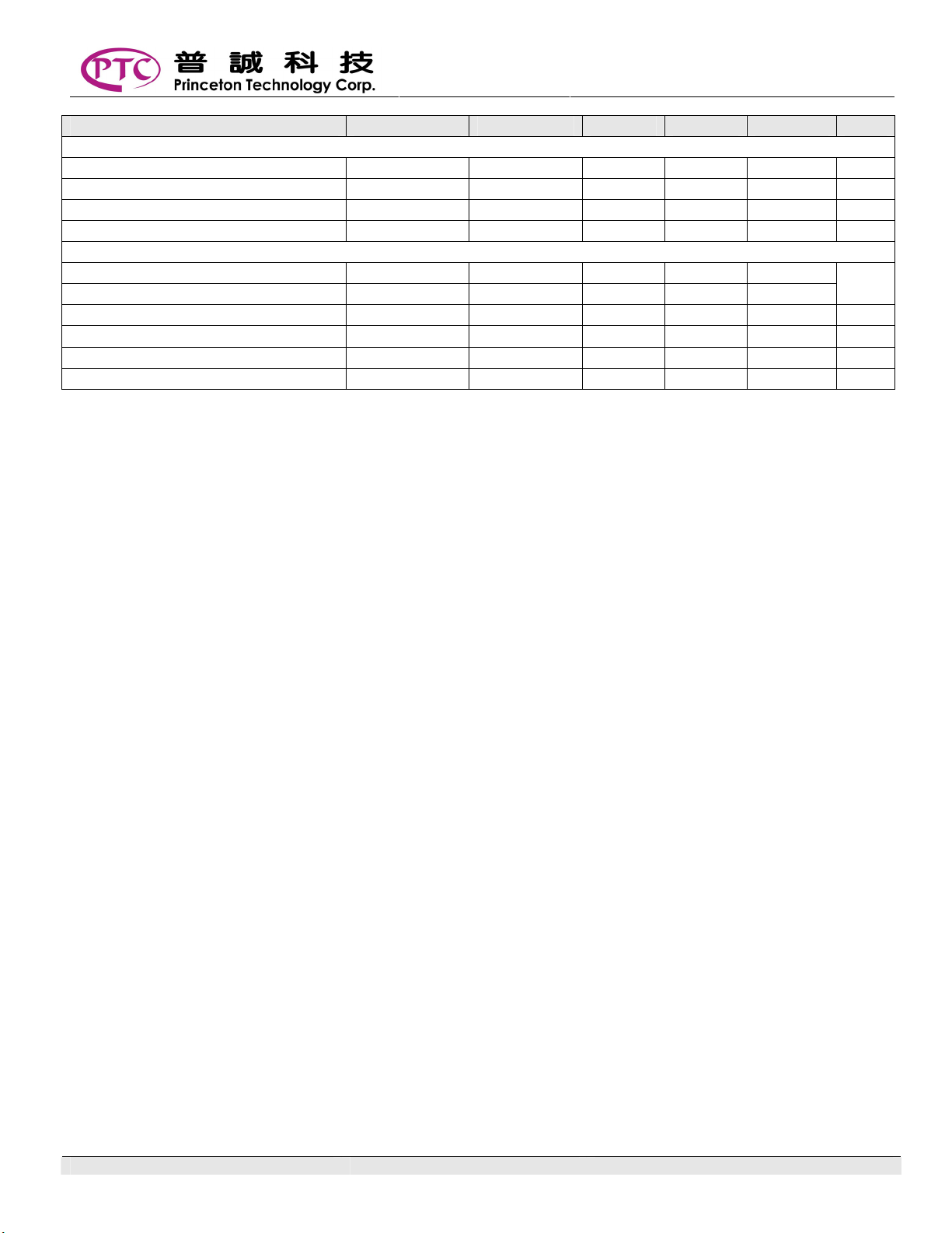
参数 符号
调光特性
调光 OTA 跨导
开环增益
在 DIM=2V,IL=0V 时,CP 电流
在 DIM=0V,IL=2V 时,CP 电流
AC 信号探测及延时
AC 输入探测比较高电压
AC 输入探测比较低电压
AC 探测有效时 VDD 最小电压
延时结束时,DL 输入比较电压
延时结束后 DL 最终电压
DL 输出电流
PT5622
测试条件 最小值 典型值 最大值 单位
Gm
Av
Icp_source
Icp_sink
ac+
V
ac-
V
V
DD-AC - 7.6 - V
DL VACDET=5V - 3.8 - V
V
V
DLF VACDET=5V - VDD - V
I
DL VDL=2V - 1 -
- 1.9 -
100 125 140
µA/V
80 85 90 dB
20 28 35
-20 -28 -35
- 4.0 -
µA
µA
V
µA
PRE1.0 8 of 14
Page 9
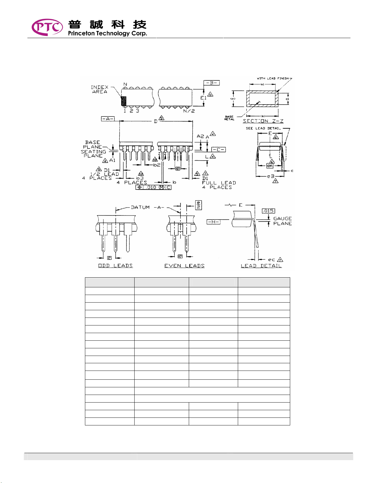
包裝資訊
16 PINS, DIP, 300MIL
PT5622
Symbol Min. Nom. Max.
A - - 0.210
A1 0.015 - A2 0.115 0.130 0.195
b 0.014 0.018 0.022
b1 0.014 0.018 0.020
b2 0.045 0.060 0.070
b3 0.030 0.039 0.045
c 0.008 0.010 0.014
c1 0.008 0.010 0.011
D 0.780 0.790 0.800
D1 0.005 - -
E 0.300 0.310 0.325
E1 0.240 0.250 0.280
e 0.100 bsc
eA 0.300 bsc
eB - - 0.430
eC 0.000 - 0.060
L 0.115 0.130 0.150
PRE1.0 9 of 14
Page 10

Notes:
1. Controlling Dimension: INCHES.
2. Dimensioning and tolerancing per ANSI Y14.5M-1982.
3. Dimensions A, A1 and L are measured with the package seated in JEDEC Seating Plane Gauge GS-3.
4. D, D1 and E1 dimensions do not include mold flash or protrusions. Mold flash or protrusions shall not exceed 0.010
inch.
5. E and eA measured with the leads constrained to be perpendicular to datum -C-.
6. eB and eA are measured at the lead tips with the leads unconstrained.
7. N is the maximum number of terminal positions (N=16).
8. Pointed or rounded lead tips are preferred to ease insertion.
9. b2 and b3 maximum dimensions do not include dambar protrusions. Dambar protrusions shall not exceed 0.010
(0.25mm).
10. Variation AB is a full lead package.
11. Distance between leads including dambar protrusions to be 0.005 in minimum.
12. Datum plane -H- coincident with the bottom of lead where lead exits body.
13. Refer to JEDEC MS-001 Variation AB.
JEDEC is the registered trademark of JEDEC SOLID STATE TECHNOLOGY ASSOCIATION.
PT5622
PRE1.0 10 of 14
Page 11
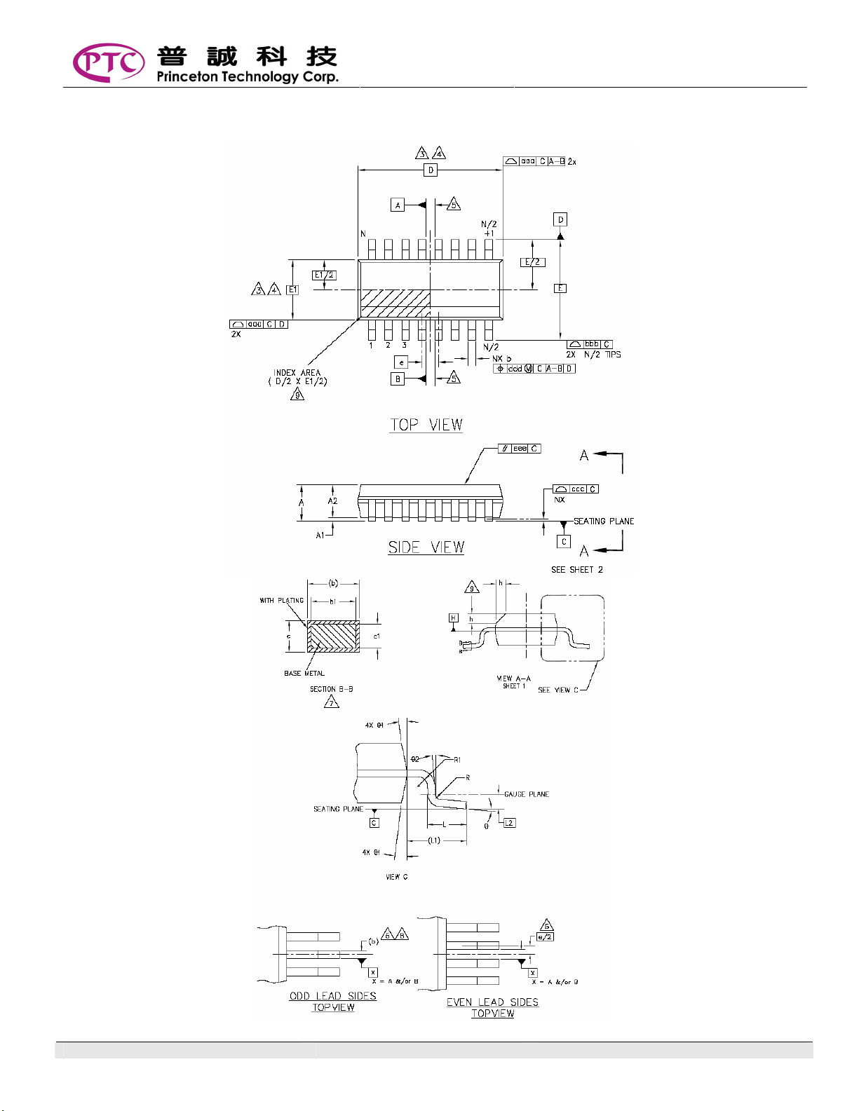
16 PINS, SOP, 150MIL
PT5622
PRE1.0 11 of 14
Page 12
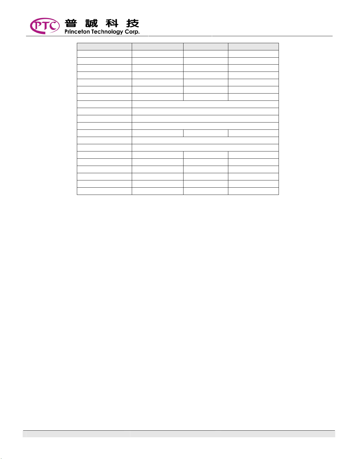
Symbol Min. Typ. Max.
A 1.35 - 1.75
A1 0.10 - 0.25
A2 1.25 - 1.65
b 0.31 - 0.51
b1 0.28 - 0.48
c 0.17 - 0.25
c1 0.17 - 0.23
D 9.90 BSC.
E 6.00 BSC.
E1 3.90 BSC.
e 1.27 BSC.
L 0.40 - 1.27
L1 1.04 REF.
L2 0.25 BSC.
R 0.07 - -
R1 0.07 -
h 0.25 - 0.50
θ 0° - 8°
θ1 5° - 15°
θ2 0° - -
Notes:
1. Dimensioning and tolerancing per ANSI Y 14.5M-1994
2. Controlling Dimension: MILLIMETERS.
3. Dimension D does not include mold flash protrusions or gate burrs. Mold flash, protrusions or gate burrs shall not
exceed 0.15 mm (0.006 in) per end. Dimension E1 does not include interlead flash or protrusion. Interlead flash or
protrusion shall not exceed 0.25mm per side. D and E1 dimensions are determined at datum H.
4. The package top may be smaller than the package bottom. Dimensions D and E1 are determined at the outermost
extremes of the plastic body exclusive of mold flash, tie bar burrs, gate burrs and interlead flash, but including any
mismatch between the top and bottom of the plastic body.
5. Datums A & B to be determined at datum H.
6. N is the number of terminal positions. (N=16)
7. The dimensions apply to the flat section of the lead between 0.10 to 0.25mm from the lead tip.
8. Dimension “b” does not include dambar protrusion. Allowable dambar protrusion shall be 0.10mm total in excess of
the “b” dimension at maximum material condition. The dambar cannot be located on the lower radius of the foot.
9. This chamfer feature is optional. If it is not present, then a pin 1 identifier must be located within the index area
indicated.
10. Refer to JEDEC MS-012, Variation AC.
JEDEC is the registered trademark of JEDEC SOLID STATE TECHNOLOGY ASSOCIATION.
PT5622
PRE1.0 12 of 14
Page 13

PT5622
IMPORTANT NOTICE
Princeton Technology Corporation (PTC) reserves the right to make corrections, modifications, enhancements,
improvements, and other changes to its products and to discontinue any product without notice at any time.
PTC cannot assume responsibility for use of any circuitry other than circuitry entirely embodied in a PTC product. No
circuit patent licenses are implied.
Princeton Technology Corp.
2F, 233-1, Baociao Road,
Sindian, Taipei 23145, Taiwan
Tel: 886-2-66296288
Fax: 886-2-29174598
http://www.princeton.com.tw
PRE1.0 13 of 14
 Loading...