

Page 1
LCD TELEVISION
LC-U# serial
Page 2

CONTENTS
Safety instructions………………………………………………………………………..…
Adjustment instructions …………………………….…….…………………………….…
Trouble shooting ……………………………………………………….……………………
Working principle analysis……………………………………………………….………….
Block diagram…………………………………..……………….……………….…………
IC block diagram………………………………………………………………………..……
Main assembly……………………………………………………………………………..…
Identification criteria for the bright spot and dark spot of the LCD screen………..….
Wiring diagram ……………………………………………………………..……………...
Troubleshooting charts………………………………………………………………..……
Schematic diagram (CPU and TV board) ……………………………………………..……
Schematic diagram (LC-23U7 and LC-27U7 power supply board)………………….…
Schematic diagram (LC-32U5 power supply board)…………………………….….…..
1
3
6
8
9
10
22
23
24
25
28
39
40
Page 3

1
Safety instructions
1. Instructions
Be sure to switch off the power supply before replacing or welding any components or
inserting/plugging in connection wire Anti static measures to be taken (throughout the entire
production process!):
a) Do not touch here and there by hand at will;
b) Be sure to use anti static electric iron;
c) It’s a must for the welder to wear anti static gloves.
Please refer to the detailed list before replacing components that have special safety requirements.
Do not change the specs and type at will.
2. Points for attention in servicing of LCD
2.1 Screens are different from one model to another and therefore not interchangeable. Be sure to
use the screen of the original model for replacement.
2.2 The operation voltage of LCD screen is 700-825V. Be sure to take proper measures in
protecting yourself and the machine when testing the system in the course of normal operation or
right after the power is switched off. Please do not touch the circuit or the metal part of the module
that is in operation mode. Relevant operation is possible only one minute after the power is
switched off.
2.3 Do not use any adapter that is not identical with the TV set. Otherwise it will cause fire or
damage to the set.
2.4 Never operate the set or do any installation work in bad environment such as wet bathroom,
laundry, kitchen, or nearby fire source, heating equipment and devices or exposure to sunlight etc.
Otherwise bad effect will result.
2.5 If any foreign substance such as water, liquid, metal slices or other matters happens to fall into
the module, be sure to cut the power off immediately and do not move anything on the module lest it
should cause fire or electric shock due to contact with the high voltage or short circuit.
2.6 Should there be smoke, abnormal smell or sound from the module, please shut the power off at
once. Likewise, if the screen is not working after the power is on or in the course of operation, the
power must be cut off immediately and no more operation is allowed under the same condition.
2.7 Do not pull out or plug in the connection wire when the module is in operation or just after the
power is off because in this case relatively high voltage still remains in the capacitor of the driving
circuit. Please wait at least one minute before the pulling out or plugging in the connection wire.
2.8 When operating or installing LCD please don’t subject the LCD components to bending, twisting
or extrusion, collision lest mishap should result.
2.9 As most of the circuitry in LCD TV set is composed of CMOS integrated circuits, it’s necessary
to pay attention to anti statics. Before servicing LCD TV make sure to take anti static measure and
ensure full grounding for all the parts that have to be grounded.
2.10 There are lots of connection wires between parts behind the LCD screen. When servicing or
moving the set please take care not to touch or scratch them. Once they are damaged the screen
Attention: This service manual is only for service personnel to take reference with. Before
servicing please read the following points carefully.
Page 4
2
would be unable to work and no way to get it repaired.
2.11 Special care must be taken in transporting or handling it. Exquisite shock vibration may lead to
breakage of screen glass or damage to driving circuit. Therefore it must be packed in a strong case
before the transportation or handling.
2.12 For the storage make sure to put it in a place where the environment can be controlled so as to
prevent the temperature and humidity from exceeding the limits as specified in the manual. For
prolonged storage, it is necessary to house it in an anti-moisture bag and put them altogether in one
place. The ambient conditions are tabulated as follows:
Temperature Scope for operation 0 ~ +50 oC
Scope for storage -20 ~ +60 oC
Humidity Scope for operation 20% ~ 85%
Scope for storage 10% ~ 90%
2.13 Display of a fixed picture for a long time may result in appearance of picture residue on the
screen, as commonly called “ghost shadow”. The extent of the residual picture varies with the
maker of LCD screen. This phenomenon doesn’t represent failure. This “ghost shadow” may remain
in the picture for a period of time (several minutes). But when operating it please avoid displaying
still picture in high brightness for a long time.
3. Points for attention during installation
3.1 The front panel of LCD screen is of glass. When installing it please make sure to put it in place.
3.2 For service or installation it’s necessary to use specified screw lest it should damage the screen.
3.3 Be sure to take anti dust measures. Any foreign substance that happens to fall down between
the screen and the glass will affect the receiving and viewing effect
3.4 When dismantling or mounting the protective partition plate that is used for anti vibration and
insulation please take care to keep it in intactness so as to avoid hidden trouble.
3.5 Be sure to protect the cabinet from damage or scratch during service, dismantling or mounting.
Page 5
3
Alignment instruction
1 Alignment equipment
PM5518 (video signal generator)
K-7253 (VGA signal generator)
CA210 (white balancer)
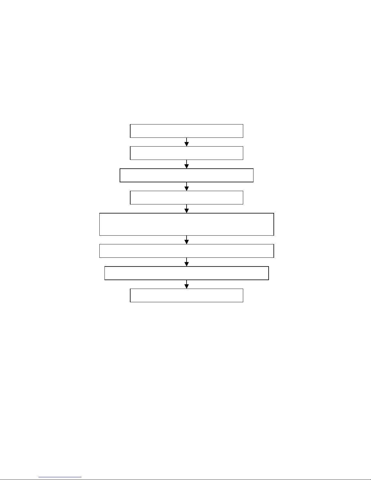
2 Alignment flow-chart
The alignment flow-chart is shown as fig-1
Fig-1 adjustment flow-chart
3 Unit adjustments
Connect digital board, CPU board and analog board according to wiring diagram, connect with
power and observe the display.
Method for entering factory menu: press “SLP”, “DSP”, “MENU” and “DSP” in turn to enter factory
menu; press “CH+” and “CH-” to select adjustment items and press “VOL+” and “VOL-” to adjust
value items, press “MENU” to exit.
Note: the white balance adjustment should be done under “nature” picture mode.
3.1 Initialization
Enter factory menu, select “Factory settings” sub-menu, and adjustment for items of table1.
Check DDC, HDCP KEY and CPU
Factory initialization setup
IF channel voltage of TV and AGC voltage adjustment
Support format of VGA pre-set
Adjustment for sub-brightness and white balance of VGA/HDMI (colo
r
temperature 6500k, 9300k and 12000k)
Adjustment for sub-brightness and white balance of YPbPr/YcbCr channel
Adjustment for sub-brightness and white balance of VIDEO channel
Preset ex-factory
Page 6
4
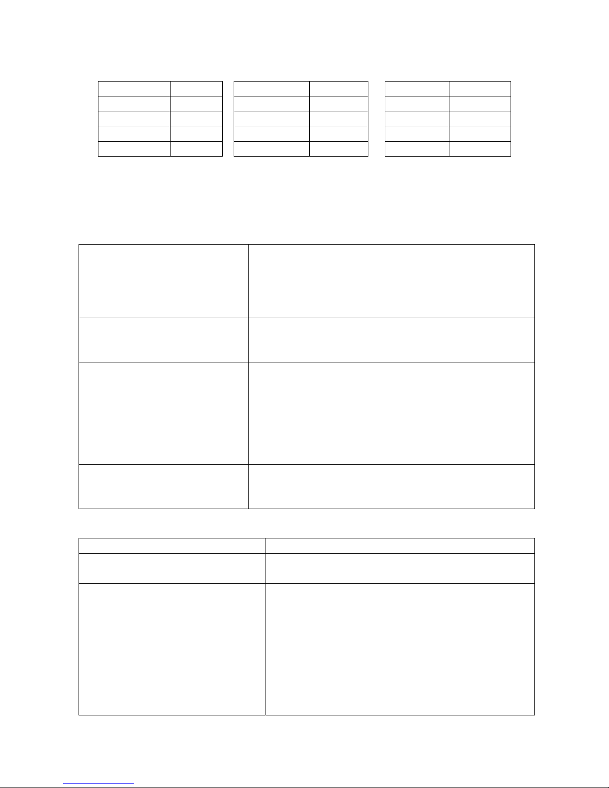
Table1 sub-menu adjustment
Items Range Introduce
PW on LOGO ON/OFF Display 5s LOGO of turn on the TV
NO Sig LOGO ON/OFF If display LOGO in no signal
Black Screen BLUE/BLACK If display blue screen and white noise wave in no signal, setting
“BLUE”
MLK 120-159 Adjustment for clock frequency (MHz) of memorizer, setting “145”.
PIP Size Middle/Large Select two component of PIP: “SMALL AND MIDDLE” and “SMALL
AND BIG”, setting “MIDDLE”.
init EEprom Start? Eeprom Initialization (adjustment for EEprom data)
3.2 Adjustment for AFT voltage and AGC voltage of IF channel in TV
Input frequency for 45.75MHz and IF signal for 80dBV of TP1, adjust L107 to value 2.4v of TP2;
when increase 0.10MHz of TP1 input signal, the TP2 value 1.0v at least; but decrease 0.10MHz of
TP1 input signal, the TP2 value 4.0v at least.
3.3 VGA/DVI channel adjustment
3.3.1 Preset VGA channel mode
Input VGA signal (PATTERN: CROSS) of VG-849 or VG-848, select PROG850(640*400/85Hz),
auto adjustment until the screen is filled with picture. Use the same method to do auto adjustment
for the following items:
PROG851(640*480/72 Hz) PROG852(640*480/75 Hz) PROG853(800*600/56 Hz)
PROG854(800*600/60 Hz) PROG855(800*600/72 Hz) PROG856(1024*768/60 Hz)
PROG857(1024*768/70 Hz) PROG858(1280*768/75 Hz) PROG888(800*600/75 Hz)
PROG915(1152*870/75 Hz) PROG915 (1280*1024/60Hz)
3.3.2 Sub-brightness and White balance adjustment VGA/HDMI channel
a. Input VG-849 or VG-848 signal of VGA: PROG852(640* 480/75Hz) and eighth level gray-scale
signal of PATTERN. Use color analyzer CA210 to adjust sub-brightness and white balance.
b. Enter submenu of COLOR TEMP., Select 9300k of color temperature, set auto value of R, G and
B to 50. Enter submenu of white balance, preset value of offset_R, offset_G and offset_B to 125,
and preset value of gain-R, gain-G and gain-B to 100. Adjustment for brightness let the second level
brightness be 3nit at least.
c. Fixed value of offset_B, adjust offset_R and offset_G, let the color coordinate of the second level
be 285 and 293 and its brightness be 4-5nit more or less (it can not 3.5nit at least). Fixed value of
gain_B, adjust gain_R, gain_G and gain_B, let the color coordinate of seventh level be 285 and 293.
Adjustment offset_R, offset_G, offset_B, gain_R, gain_G and gain_B repeatedly until the value of
the two levels gray-scale be 285 and 293.
d. Select 6500k of color temperature, set auto value of R, G and B to 50. Fixed value of B to 50,
adjust R and G, let the color coordinate of the sixth level be 313 and 329. Adjust R and G repeatedly
until the color coordinate value to 313 and 329.
e. Select 12000k of color temperature, set auto value of R, G and B to 50. Fixed value of B to 50,
adjust R and G, let the color coordinate of the sixth level be 270 and 283. Adjust R and G repeatedly
until the color coordinate value to 270 and 283.
Page 7

5
f. Input PROG852(640*480/75Hz) and the eighth level gray-scale of PATTERN signal of VG-849 to
HDMI, repeatedly the b-e course. In the HDMI channel, preset value of offset_R, offset_G and
offset_B to 15, preset value of gain_R, gain_G and gain_B to 25.
3.4 Adjustment for sub-brightness and white balance of YPbPr channel
a. Connect YPbPr signal of VG-849 and VG-848 to YPbPr terminal, input color signal of
PROG973(1080i)PATTERN964. Select AUTOTUNE item, wait for it displays “OK”. NOTE: Don’t
select AUTOTUNE item in other state.
b. Switch YPbPR signal of VG-849 and VG-848 output to the eighth gray-scale signal of
PROG973(1080i)PATTERN964. prset value of offset_R, offset_G and offset_B to 15 and gain-R,
gain-G and gain-B to 25. adjust brightness, let second bright to 3nit at least.
c. Fixed value of offset_B, adjust offset_R and offset_G, let the color coordinate of the second level
be 285 and 293 and its brightness be 4-5nit more or less (it can not 3.5nit at least). Fixed value of
gain_B to 25, adjust gain_R, gain_G and gain_B, let the color coordinate of seventh level be 285
and 293. Adjustment offset_R, offset_G, gain_R and gain_G repeatedly until the value of the two
levels gray-scale be fixed.
d. Input PROG977(720p), PROG978(480p) and PROG968(480i) mode for eighth level gray-scale
signal, let the color coordinate of the second level and the seventh level 285 and 293.
3.5 VIDEO channel adjustment (TV/VIDEO/S-VIDEO)
a. Connect color bar signal of AV (PM5518, NTSC , eight level gray-scale signal) to VIDEO1
terminal, enter factory menu, preset value of offset_R, offset_G and offset_B to 15 and gain-R,
gain-G and gain-B to 25, adjust brightness, let second bright to 3nit at least.
b. Fixed value of offset-B to 15, adjust offset_R and offset_G, let the color coordinate of the second
level be 285 and 293 and its brightness be 4-5nit more or less (it can not 3.5nit at least). Fixed value
of gain_B to 25, adjust gain_R, gain_G and gain_B, let the color coordinate of seventh level be 285
and 293. Adjustment offset_R, offset_G, gain_R and gain_G repeatedly until the value of the two
levels gray-scale be fixed.
4 Performance check
4.1 TV function
Enter searching menu → auto search, connect RF-TV terminal with central signal source and check
if there are channels be skipped
4.2 AV/S, YpbPr terminals
Input AV/S, HD signal, check if it is normal.
4.3 VGA terminal
Insert VGA terminal, input VGA format signal of 640 X 480@60 Hz, check if the display is normal. If
interference exists, press the auto adjusts button on remote control again and check if it is normal.
4.4 HDMI terminal
Insert HDMI terminal, input signal of 640 X 480@60 Hz signal and check if the display is normal.
4.5 check sound channel
Check the speaker and headphone of each channel.
4.6 presetting before ex-factory
Page 8
6
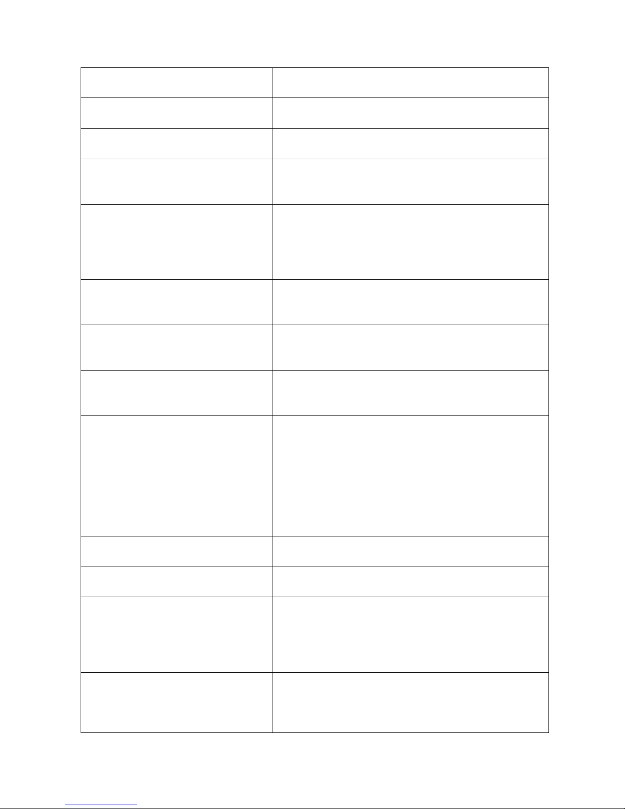
Tr ouble shooting
Before servicing please check to find the possible causes of the troubles according to the table
below.
1.Antenna(signal):
Picture is out of focus or jumping Bad status in signal receiving
Poor signal
Check if there are failures with the electrical connector or
the antenna.
Check if the antenna is properly connected.
Fringe in picture Check if the antenna is correctly oriented.
Maybe there is electric wave reflected from hilltop or
building.
Picture is interfered by stripe
shaped bright spots
Possibly due to interference from automobile, train, high
voltage transmission line, neon lamp etc.
Maybe there is interference between antenna and power
supply line. Please try to separate them in a longer
distance.
Maybe the shielded-layer of signal wire is not connected
properly to the connector.
There appear streaks or light color
on the screen
Check if interfered by other equipment and if interfered
possibly by the equipment like transmitting antenna,
non-professional radio station and cellular phone.
2.TV set:
Symptoms Possible cause
Unable to switch the power on Check to see if the power plug has been inserted
properly into the socket.
No picture and sound Check to see if the power supply of liquid crystal TV
has been switched on. (As can be indicated by the
red LED at the front of the TV set)
See if it’s receiving the signal that is transmitted from
other source than the station
Check if it’s connected to the wrong terminal or if the
input mode is correct.
Check if the signal cable connection between video
source and the liquid crystal TV set is correct.
Item Setting Item Setting Item Setting
Picture mode NATURE OSD language English CCD OFF
Sound mode NORMAL HALFTONE 50 STEREO ON
N/R WEAK DURATION 30 VGA/HDMI NORMAL
SCREEN FULL MAG.C ON ANTENNA CATV
Page 9
7
Deterioration of color phase or color
tone
Check if all the picture setups have been corrected.
Screen position or size is not proper Check is the screen position and size is correctly set
up.
Picture is twisted and deformed Check to see if the picture-frame ratio is properly set
up.
Picture color changed or colorless Check the “Component” or “RGB” settings of the
liquid crystal TV set and make proper adjustment
according to the signal types.
Picture too bright and there is
distortion in the brightest area
Check if the contrast setting is too high.
Possibly the output quality of DVD broadcaster is set
too high.
It maybe also due to improper terminal connection of
the video signal in a certain position of the system.
Picture is whitish or too bright in the
darkest area of the picture
Check if the setting for the brightness is too high
Possibly the brightness grade of DVD player
(broadcaster) is set too high.
No picture or signal produced from the
displayer if “XXX in search” appears.
Check if the cable is disconnected.
Check if it’s connected to the proper terminal or if the
input mode is correct.
There appears an indication - “outside
the receivable scope)
Check if the TV set can receive input signal. The
signal is not correctly identified and VGA format is
beyond the specified scope.
Remote control cannot work properly Check if the batteries are installed in the reverse
order.
Check if the battery is effective.
Check the distance or angle from the monitor.
Check if there is any obstruct between the remote
control and the TV set.
Check if the remote control signal- receiving window
is exposed to strong fluorescence.
No picture and sound, but only hash. Check if the antenna cable is correctly connected, or
if it has received the video signal correctly.
Blur picture Check if the antenna cable is correctly connected.
Of if it has received the right video signal.
No sound Check if the “mute” audio frequency setting is
selected.
Check if the sound volume is set to minimum.
Make sure the earphone is not connected.
Check if the cable connection is loose.
When playing VHS picture search
tape, there are lines at the top or
bottom of the picture.
When being played or in pause VHS picture search
tape sometimes can’t provide stable picture, which
may lead to incorrect display of the liquid crystal TV,
In this case please press “auto” key on the remote
Page 10

8
control so as to enable the liquid crystal TV set to
recheck the signal and then to display correct picture
signal
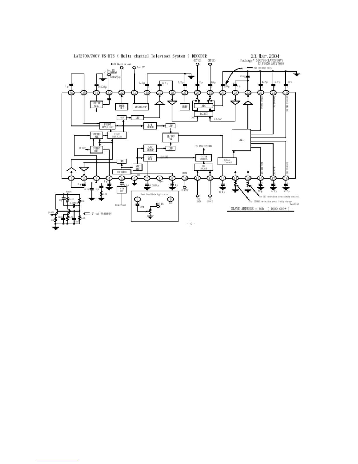
Working principle analysis
RF signal from the antenna to tuner, via high frequency amplifier and mix frequency to obtain IF
signal, and then via pre-IF amplifier in V104, then it send to processed IF filter of SAW (Z103),
obtain more idea IF speciality, it processed to IF amplifier, phase locked logic VCO and sync
detection of N101 (M52760E) in the TV board to obtain VIDEO; IF via pre IF amplifier to send to
processed filter of SAW (Z102), again send to processed IF amplifier of N101, decode second SIF.
From M52760E output VIDEO, AV1 and AV2/S signal all send to video decoder N601
(TVP5147PFP), via video select, clamping, A/D transfer, comb filter and color decode, one way
output AV OUT, another way output 8bit for CIR656 format signal and CLK signal, send to
N101(MST6151) of CPU board, Also YPbPr, VGA and HDMI send to N101. N101(MST6151) is
many function big dimension integrate circuit, it processed HDMI, A/D to DA switch, interlaced and
non-interlaced processing, model switch and low voltage difference output functions and so on, it
send to four ways difference signal and one way clock signal to LCD display.
From HDMI input to MST6151contain sound signal, via processed MST6151, send to processed
D/A switch for NA01(CS4340), output L/R of HDMI.
Output SIF from M52760F and send to processed stereo demodulation for N201(LA72700), output
L/R of TV.
L/R of HDMI and Ypbpr from CS4340 output, L/R of VGA/DVI signal via sound switch
NA02(HEF4052) to select, then send to sound processing N301(R2S15900SP); demodulate L/R
signal of LA72700 send to N301, and L/R signal for AV1A and V2/S input send to N301. Via
selected switch and processing sound, one way sound output for AV OUT, other way send to
N401(TPA3008D2) of sound amplifier, via amplify for sound signal to speaker and earphone.
The unit working is controlled N801(MTV412) of CPU, connect tuner, TVP5147, LA72700 and
R2S15900SP to IIC bus; connect MST6151 to parallel BUS.
Page 11
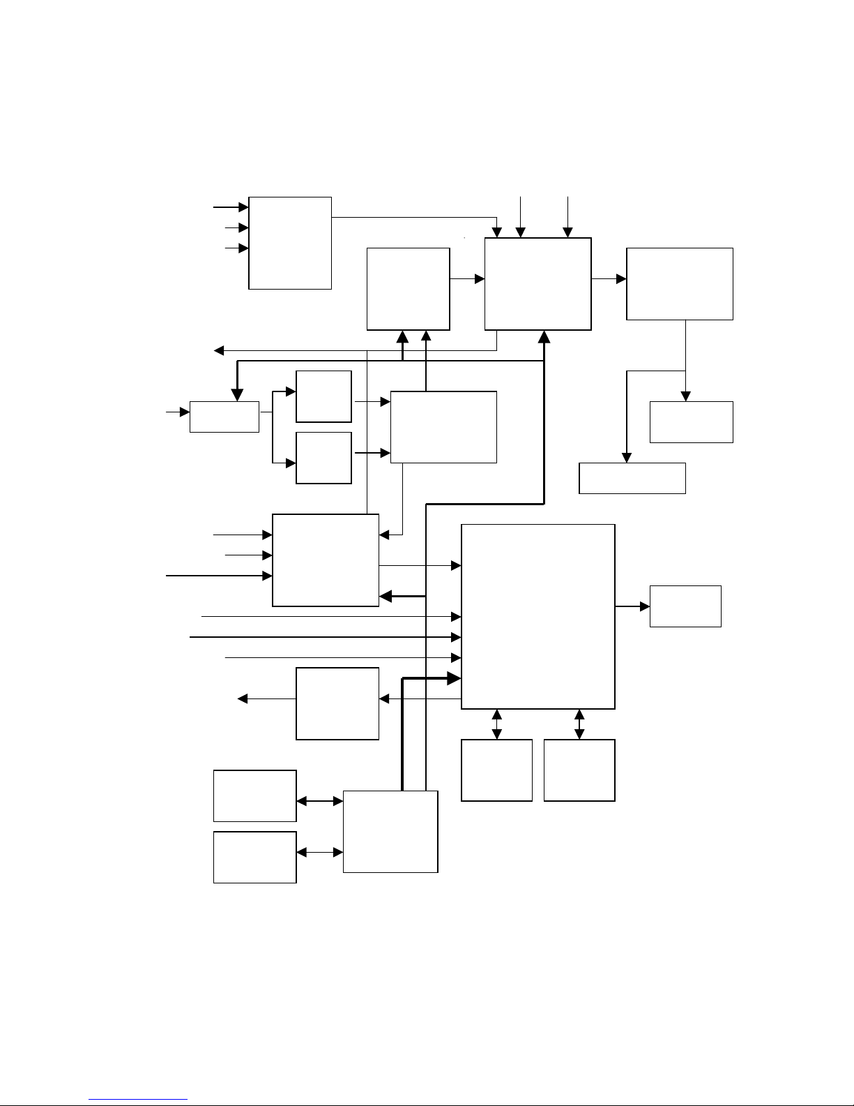
BLOCK DIAGRAM
AV1-A AV2/S-A
YPbPr-A
VGA/DVI-A L/R
HDMI-A
L/R
A
AV OUT L/R
SIF
RF
IF
V
V IIC
VIDEO1
Y/VIDEO2 CCIR656
C 8bit
YPbPr
VGA
HDMI/DVI
HDMI-A
L/R
BUS
SCALER
A/D D/A
DEINTERLACER
LVDS
HDMI
N
101(CPU)
MST6151DA
VIDEO
DECORDER
N
601
TVP5147PFP
MCU
N
801
MTV412
SDRAM
N
201
SDRAM
N
202
SIF DEC
N
201
LA72700
AUDIO
PROCESSO
R
N
301
R2S15900SP
AUDIO AMP
N
401
TPA3008D2
EEPROM
N
802
EEPROM
N
803
AUDIO
SW
N
A02
HEF4052
IF AMP
N
101(TV)
M52760E
TUNER
SAW
Z103
SAW
Z102
SPEAKER
PANEL
DAC
N
A01
CS4340
HEADPHONE
9
Page 12
10
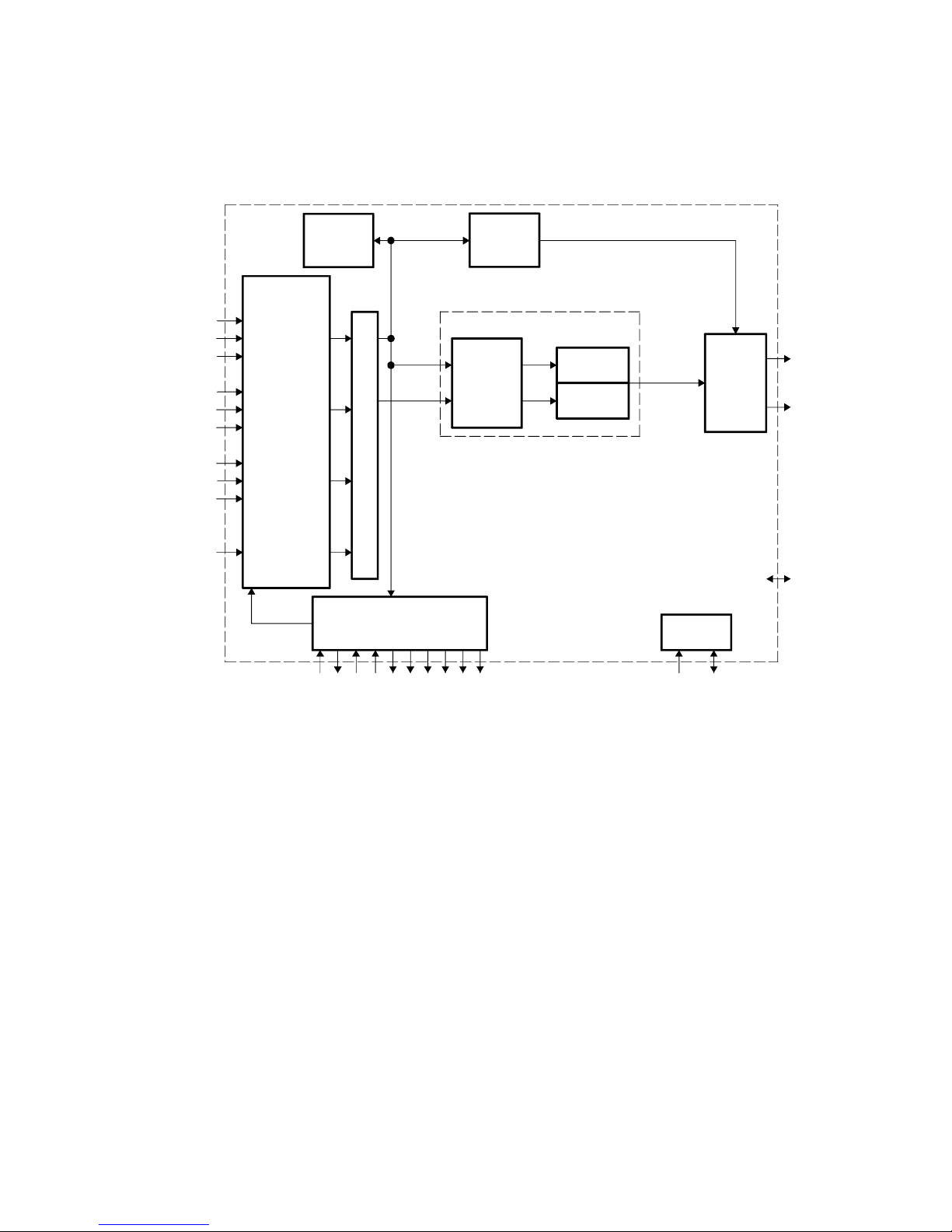
IC block diagram
TVP5147
Composite and S-Video Processor
Y/C
Separation
5-li ne
Adaptive
Comb
Luma
Processing
Chroma
Processin
g
M
U
X
CVBS/Y
C/CbCr
C
Y
Output
Formatter
Y[9:0]
VBI
Data
Proces s o r
Copy
Prot ection
Detector
C[9:0]
Host
Interface
Timing Proces sor
With Sync Detector
VI_1_A
VI_1_B
VI_1_C
VI_2_A
VI_2_B
VI_2_C
VI_3_A
VI_3_B
VI_3_C
VI_4_A
CVBS/
Y
CVBS/
C/Pb
CVBS/
C/Pr
CVBS/Y
CVBS/Y
Analog
Front End
Sampling
Clock
GPIO
HS/CS
VS/VBLK
FID
AVID
XTAL1
XTAL2
DAT ACLK
RESETB
GLCO
PWDN
SCL
SDA
YCbCr
Clamping
AGC
2 11-Bit
ADC
80: A V OUT
2: TV-V input
7: A V1-V input
9: A V2-V/S-Y input
18: S-C input
29: SDA
28: SCL
40: CLK output
43-47, 50-52: CCIR656 format signal output
4, 5, 20, and 21: 3.3V-A power supply
38, 48, 61: 3.3V-D power supply
11, 25, 76: 1.8V-A power supply
31, 41, 55, and 67: 1.8V-B power supply
Page 13

11
M52760
2: AFT
3: AGC
4, 5: picture If input
7: sound IF input
13: SIF output
10: mono sound output
18: TV- VIDEO output
14, 17: +5V-1 power supply
Page 14
12
LA72700
5: SIF input
25: TV sound -R output
26: TV sound- L output
11: SDA
12: SCL
31: +9Vpower supply
Page 15

13
MST6151
207, 208: HDMI-R input
2, 3: HDMI-G input
5, 6: HDMI-B input
8, 9: HDMI-CLK input
14: HDMI-SDA
15: HDMI-SCL
20, 21: VGA-B input
22: VGA-G input
23, 24: VGA-G input
25, 26: VGA-R input
18: VGA H-sync input
19: VGA V-sync input
27, 28: PB input
29, 30: Y input
31: HDMI-G input
32, 33: PR input
54-61: CCIR656 format signal input
53: CLK input
164-171, 174: 4 difference signal output
160, 161: 1 clock signal output
188-191: HDMI sound output
200: PWW (brightness control switch) output
72-75: BUS (parallel communication signal)
49, 131, 195: 1.8V power supply
4,17,12,109,204,66,102: 3.3V power supply
Page 16

14
PIN DIAGRAM (MST5151A)
Pin 1
1
2
3
4
5
7
9
11
13
14
17
18
21
23
25
27
28
30
32
34
36
39
41
43
6
8
10
12
15
16
19
20
22
24
26
29
31
33
35
37
38
40
42
44
45
46
47
48
50
51
52
49
5354555657
59
61
636566
69
70
73
75
777980
82
84
86
88
91
93
95
58
60
62
64
67
68
717274
76
78
81
83
85
878990
92
9496979899
100
102
103
104
101
208
207
206
205
204
202
200
198
196
195
192
191
188
186
184
182
181
179
177
175
173
170
168
166
203
201
199
197
194
193
190
189
187
185
183
180
178
176
174
172
171
169
167
165
164
163
162
161
159
158
157
160
156
155
154
153
152
150
148
146
144
143
140
139
136
134
132
130
129
127
125
123
121
118
116
114
151
149
147
145
142
141
138
137
135
133
131
128
126
124
122
120
119
117
115
113
112
111
110
109
107
106
105
108
MVREF
GND
VDDM
MST5151A
XXXXXXXXXXX
XXXXX
GND
AVDD_MPLL
XIN
XOUT
PWM1
PWM0
AIWS
AISCK
VDDC
SPDIFO
AUWS
AUSD
LVB0M
VDDC
GND
VDDP
AISD
AIMCK
GND
AUMUTE
AUSCK
AUMCK
LVB0P
GND
LVB1M
LVB1P
LVB2M
LVB2P
LVBCKM
LVBCKP
LVB3M
LVB3P
VDDC
GND
LVA0M
LVA0P
LVA1M
LVA1P
LVA2M
LVA2P
LVACKM
LVACKP
GND
VDDP
LVA3M
LVA3P
GND
BYPASS
GND
DVI_R-
DVI_R+
GND
GND
DVI_G+
DVI_G-
AVDD_DVI
DVI_B+
DVI_CK+
AVDD_DVI
AVDD_PLL
DDCD_DA
GND
HSYNC1
BIN1P
BIN1M
DVI_B-
GND
DVI_CK-
REXT
GND
DDCD_CK
AVDD_ADC
VYSNC1
SOGIN1
GIN1P
GIN1M
RIN1P
RIN1M
BIN0M
BIN0P
GIN0M
GIN0P
SOGIN0
RIN0M
RIN0P
AVDD_ADC
GND
HSYNC0
VSYNC0
RMID
REFP
REFM
VI_DATA[8]
VI_DATA[9]
VI_DATA[10]
VI_DATA[11]
VI_DATA[12]
VI_DATA[13]
VI_DATA[14]
VI_DATA[15]
AVDD_APLL
GPO[5]
GPO[4]
GND
VI_CK
VI_DATA[0]
VI_DATA[1]
VI_DATA[2]
VI_DATA[3]
VI_DATA[4]
VI_DATA[7]
GND
VDDP
INT
RDZ
DBUS[0]
DBUS[1]
VI_DATA[5]
VI_DATA[6]
VDDC
GND
HWRESET
ALE
WRZ
DBUS[2]
DBUS[3]
GPO[3]
GPO[2]
GPO[1]
VDDC
GND
MDATA[31]
MDATA[30]
MDATA[29]
MDATA[28]
VDDM
GND
MDATA[27]
MDATA[26]
MDATA[25]
MDATA[24]
MDATA[23]
MDATA[22]
MDATA[21]
MDATA[20]
MDATA[19]
MDATA[18]
MDATA[17]
MDATA[16]
DQS[2]
VCTRL
DQS[3]
DQM[1]
DQS[0]
MDATA[0]
GND
VDDC
MADR[10]
MADR[9]
MADR[8]
GND
VDDM
MADR[7]
MADR[6]
MADR[5]
MADR[4]
MADR[3]
MADR[2]
MADR[1]
MADR[0]
WEZ
CASZ
GND
VDDM
RASZ
BADR[0]
BADR[1]
AVDD_PLL2
GND
MCLK
MCLKZ
MCLKE
MDATA[1]
MDATA[2]
MDATA[3]
MDATA[4]
MDATA[5]
MDATA[6]
MDATA[7]
MDATA[8]
MDATA[9]
MDATA[10]
MDATA[11]
GND
VDDM
MDATA[12]
MDATA[13]
MDATA[14]
MDATA[15]
DQS[1]
DQM[0]
MADR[11]
VDDC
GND
VDDM
Page 17

15
PIN DESCRIPTION
MCU Interface
Pin Name Pin Type Function Pin
HWRESET
Schmitt Trigger Input
w/ 5V-tolerant
Hardware Reset, active high 67
DBUS[3:0] I/O w/ 5V-tolerant MCU 4-bit DDR Direct bus; 4mA driving strength 75-72
ALE I w/ 5V-tolerant MCU Bus ALE, active high 69
RDZ I w/ 5V-tolerant MCU Bus RDZ, active high 70
WRZ I w/ 5V-tolerant MCU Bus WDZ, active high 71
INT Output MCU Bus Interrupt; 4mA driving strength 68
Analog Interface
Pin Name Pin Type Function Pin
RMID Mid-Scale Voltage Bypass 38
REFP Internal ADC Top De-coupling Pin 39
REFM Internal ADC Bottom De-coupling Pin 40
REXT Analog Input External Resister 390 ohm to AVDD_DVI 11
HSYNC0
Schmitt Trigger Input w/
5V-tolerant
Analog HSYNC Input from Channel 0 36
VSYNC0
Schmitt Trigger Input w/
5V-tolerant
Analog VSYNC Input from Channel 0 37
BIN0M Analog Input Reference Ground for Analog Blue Input from Channel 0 27
BIN0P Analog Input Analog Blue Input from Channel 0 28
GIN0M Analog Input Reference Ground for Analog Green Input from Channel 0 29
GIN0P Analog Input Analog Green Input from Channel 0 30
SOGIN0 Analog Input Sync On Green Input from Channel 0 31
RIN0M Analog Input Reference Ground for Analog Red Input from Channel 0 32
RIN0P Analog Input Analog Red Input from Channel 0 33
HSYNC1
Schmitt Trigger Input w/
5V-tolerant
Analog HSYNC Input from Channel 1 18
VSYNC1
Schmitt Trigger Input w/
5V-tolerant
Analog VSYNC Input from Channel 1 19
BIN1P Analog Input Analog Blue Input from Channel 1 20
BIN1M Analog Input Reference Ground for Analog Blue Input from Channel 1 21
SOGIN1 Analog Input Sync On Green Input from Channel 1 22
GIN1P Analog Input Analog Green Input from Channel 1 23
GIN1M Analog Input Reference Ground for Analog Green Input from Channel 1 24
RIN1P Analog Input Analog Red Input from Channel 1 25
RIN1M Analog Input Reference Ground for Analog Red Input from Channel 1 26
Page 18

16
DVI Interface
Pin Name Pin Type Function Pin
DVI_R+ Input DVI Input Channel Red + 207
DVI_R- Input DVI Input Channel Red - 208
DVI_G+ Input DVI Input Channel Green + 2
DVI_G- Input DVI Input Channel Green - 3
DVI_B+ Input DVI Input Channel Blue + 5
DVI_B- Input DVI Input Channel Blue - 60
DVI_CK+ Input DVI Input Clock + 8
DVI_CK- Input DVI Input Clock - 9
Video Interface
Pin Name Pin Type Function Pin
VI_CK Input w/ 5V-tolerant Digital Video Input Clock 66
VI_DATA[15:0] Input w/ 5V-tolerant Digital Video Input Data[15:0] 48-41, 61-54
Digital Audio Interface
Pin Name Pin Type Function Pin
AUMCK Output Audio Master Clock Output 188
AUSD Output Audio Serial Data Output; 4mA driving strength 189
AUSCK Output Audio Serial Clock Output; 4mA driving strength 190
AUWS Output Word Select Output; 4mA driving strength 191
AUMUTE Output Audio Output Mute Control 192
SPDIFO Output S/PDIF Audio Output; 4mA driving strength 193
AIMCK Input Audio Master Clock Input 196
AISD Input Audio Serial Data Input 197
AISCK Input Audio Serial Clock Input 198
AIWS Input Word Select Input 199
LVDS Interface
Pin Name Pin Type Function Pin
LVA0M Output A-Link Negative LVDS Differential Data Output 171
LVA0P Output A-Link Positive LVDS Differential Data Output 170
LVA1M Output A-Link Negative LVDS Differential Data Output 169
LVA1P Output A-Link Positive LVDS Differential Data Output 168
Page 19

17
Pin Name Pin Type Function Pin
LVA2M Output A-Link Negative LVDS Differential Data Output 167
LVA2P Output A-Link Positive LVDS Differential Data Output 166
LVA3M Output A-Link Negative LVDS Differential Data Output 161
LVA3P Output A-Link Positive LVDS Differential Data Output 160
LVACKM Output A-Link Negative LVDS Differential Data Output 165
LVACKP Output A-Link Positive LVDS Differential Data Output 164
LVB0M Output B-Link Negative LVDS Differential Data Output 187
LVB0P Output B-Link Positive LVDS Differential Data Output 186
LVB1M Output B-Link Negative LVDS Differential Data Output 181
LVB1P Output B-Link Positive LVDS Differential Data Output 180
LVB2M Output B-Link Negative LVDS Differential Data Output 179
LVB2P Output B-Link Positive LVDS Differential Data Output 178
LVB3M Output B-Link Negative LVDS Differential Data Output 175
LVB3P Output B-Link Positive LVDS Differential Data Output 174
LVBCKM Output B-Link Negative LVDS Differential Data Output 177
LVBCKP Output B-Link Positive LVDS Differential Data Output 176
GPO Interface
Pin Name Pin Type Function Pin
PWM0 Output GPO with PWM Function; 4mA driving strength 200
PWM1 Output GPO with PWM Function; 4mA driving strength 201
GPO[1] I/O GPO / FIELD input; 4mA driving strength 78
GPO[2] I/O GPO / Digital VSYNC Input; 4mA driving strength 77
GPO[3] I/O GPO / DE Input; 4mA driving strength 76
GPO[4] I/O GPO / Secondary Video Clock Input
; 4mA driving
strength
52
GPO[5] I/O GPO / Digital HSYNC Input; 4mA driving strength 51
DRAM Interface
Pin Name Pin Type Function Pin
MVREF Input
Reference Voltage for DDR SDRAM
Interface
104
MCLKE Output DRAM Memory Clock Enable 105
MCLKZ Output
DRAM Memory clock Complementary /Input
106
Page 20

18
Pin Name Pin Type Function Pin
(for differential clocks)
MCLK Output DRAM Memory Clock 107
RASZ Output Row Address Strobe, active low 112
CASZ Output Column Address Strobe, active low 115
WEZ Output Write Enable, active low 116
DQM[1:0] Output Data Mask Byte Enable 101, 133
DQS[3:0] Output Data Strobe 81, 100, 134, 153
BADR[1:0] Output Memory Bank Address 110, 111
MADR[11:0] Output Memory Address 130-127, 124-117
MDATA[31:0] I/O Memory Data 82-85, 88-
99,
135-138, 141-152
Misc. Interface
Pin Name Pin Type Function Pin
XIN Crystal Oscillator Input Crystal Oscillator Input 203
XOUT Crys
tal Oscillator
Output
Crystal Oscillator Output 202
DDCD_DA I/O w/ 5V-tolerant HDCP Serial Bus Data /
DDC data of DVI port; 4mA
driving strength
14
DDCD_CK Input w/ 5V-Tolerant HDCP Serial Bus Clock / DDC Clock of DVI Port 15
BYPASS For External Bypass Capacitor 158
VCTRL Output Regulator Control 62
Power Pins
Pin Name Pin Type Function Pin
AVDD_DVI 3.3V Power DVI Power 4, 10
AVDD_ADC 3.3V Power ADC Power 17, 34
AVDD_PLL 3.3V Power PLL Power 12
AVDD_PLL2 3.3V Power PLL Power 109
AVDD_APLL 1.8V Power Audio PLL Power 49
AVDD_MPLL 3.3V Power PLL Power 204
VDDM
3.3V Power (SDR SDRAM) /
2.5V Power (DDR SDRAM)
DRAM Interface Power
86, 102, 113, 125, 139,
154
VDDP 3.3V Power Digital Output Power 66, 162, 182
VDDC 1.8V Power Digital Core Power 63, 7
9, 131, 156, 173,
185, 195
Page 21

19
Pin Name Pin Type Function Pin
GND Ground Ground
1, 7, 13, 16, 35, 50, 64,
65, 80, 87, 103, 108,
114, 126, 132, 140,
155, 157, 159, 163,
172, 183, 184, 194,
205, 206
Page 22

20
R2S15900
2: input L of AV1
27: input R of AV1
3: input L of AV2/S
26: input R of AV2/S
4: input L of YPBPR/VGA/HDMI
25: input R of YPBPR/VGA/HDMI
Page 23

21
5: input L of TV
24: input R of TV
6: output L of AVOUT
23: output R of AVOUT
11: L output
19: R output
18: SCL
17: SDA
28: +9Vpower supply
TPA3008
1: MUTE
3: R input
5: L input
20, 17: L input
41, 44: R input
15, 23, 33, 39, and 47: +18V power supply
Page 24

22
Main assembly
NAME NO. MAIN COMPONENT AND it’S NO.
TV board 667-L27U6-40 N101
N201
N301
N401
M52760 (352-52760-10)
LA72700 (353-72700-10)
R2S15900 (353-15900-10)
TPA3008D2 (353-30080-10)
CPU board 667-L27U6-56 N101
N601
NA01
N801
MST6151DA (353-61510-10)
TVP5147 (353-51470-10)
CS4340 (353-43400-30)
MTV412 (353-04120-10)
Keypad board 667-L27U6-05
Remote control 301-RL27U6-27M (RC-R27M)
MODEL LC-23U7
(203-L27U70-01)
LC-23U7
(203-L27U70-02)
LC-27U6/27U7 LC-32U5
Power supply
board
667-L27U6-20 667-L23U6-20 667-L27U6-20 667-L32K5-20
IR board 667-L27U6-09 667-L27U6-09 667-L27U6-09 667-L32U5-09
Panel 335-23002-00 335-23004-00 335-27001-00 335-32002-00
Page 25

23
Identification criteria for the bright spot and dark spot of the LCD screen
Q’ty allowed Distance between two spots
Category criteria
15" 20" 22" 30" 40" 15" 20" 22" 30" 40"
One single
spot
≤5 ≤2 ≤5 ≤2 ≤3
2 neighboring
spots
≤2 ≤1 ≤2 ≤1 ≤1
Bright
spo
t
Total No. ≤5 ≤2 ≤5 ≤2 ≤3
≥15mm
One single
spot
≤6 ≤7 ≤5 ≤4 ≤10
Two
neighboring
spots
≤2 ≤2 ≤2 ≤1 ≤5
Dark
spots
Total No. ≤6 ≤7 ≤5 ≤4 ≤10
≥15mm
≥10mm
≥5mm
Total defected point ≤8 ≤7 ≤5 ≤4 /
Notes:
1. Definition of defected point (bright spot, dark spot): It is identified as a defected point if its area
exceeds 1/2 of a single picture element (R,G,B).
2. Definition of bright spot: It is identified as a bright spot if it is bright in the state of dark field and its
bright size remains unchanged
3. Definition of dark spot: It is identified as a dark spot if it is dark in the state of white field and its
dark size remains unchanged
4. Definition of two neighboring points: Defects of a group of picture elements(RB,RG,GB).
Page 26

24
Wiring diagram
Page 27

25
Troubleshooting guide
1. No raster
Turn-on power supply, chec
k
if the red indicator is light in
the STANDBY?
Check if PIN8(5V) of CPU
board is normal?
Check STANDBY circuit o
f
power supply board
Press POWER button in the
unit button and sensor control,
check the indicator.
Check if the PIN12 of X503 in
CPU board is high-level?
Check if the PIN12 of X501 i
n
CPU board is high-level?
Check power supply board
Check back light board
yes
no
no
blue
red
no
yes
Replacing N801
no
yes
Page 28

26
2. Raster, but no picture
Check if the unit butto
n
and sensor control
operation?
Check if the all
channels have signal?
Replacing
CPU board
Enter factory-menu,
initialization EEPROM,
then turn off the TV,
turn on again, displa
y
picture?
Adjust CPU boar
d
again
Which is no
signal o
f
channels
Replacing
CPU board
Check if 1VPP signal
and noise wave o
f
X12 (PIN 1) in the
TV board?
Check if outpu
t
IF signal o
f
TUNER1 (pi
n
11) is normal?
Replacing
TUNER1
Check N101
no
yes
yes
HDMI/VGA/YPRP
TV
yes
no
no
no
yes
Does display OSD
menu in screen whe
n
press submenu?
yes
no
yes
Page 29

27
3.no sound
Check if PIN15, PIN30
and PIN38 voltage o
f
N
401 is normal?
Check power supply
Check PIN11 an
d
PIN19 output wave o
f
N
301
Check PIN25 an
d
PIN26 output wave o
f
N
201
Check PIN5 wave o
f
N
201
Check PIN11 wave of
TUNER1
Replacing N401
Replacing N301
Replacing N201
no
yes
no
yes
yes
yes
no
no
Replacing TUNER1
no
Page 30

Page 31

Page 32

Page 33

Page 34

Page 35

Page 36

Page 37

Page 38

Page 39

Page 40

Page 41

Page 42

5
5
4
4
3
3
2
2
1
1
D D
C C
B B
A A
3
3
BAS21
C
J1
1
1
2
TOP
1
1
2
3
E
TL431
2
TOP
TOP
2
TOP
BCX53-16
TOP
MUR860
BCX56-16
ISL9R1560G2
1
12
B
J1
0.35mm 辅铜
KAS200-5S242212
A0
PFC INPUT AND STNADBY
LC-32U5 POWER SUPPLY BOARD
A3
23Tuesday, March 15, 2005
Title
Size Document Number Rev
Date: Sheet
of
VCC1
B
A
ON_OFF_1
PFC 3
VCC1_1 3
A3
B3
D13
ON_OFF 3
STD-5V
STD-5V
R932
330K ±5%
D903
1N4007
1 2
R920
10 ±5%
C907
1000PF/50V
R969
5.1K ±5%
R927
360K ±5%
D908
BAS21
1 3
2
C917
100PF/50V
C918
0.22UF/50V 1206
R968
100K ±5%
Q908
BCX56-16
3
21
PFC
TEST
1
1
R936
360K ±5%
JP?
JUMPER
1 2
+
E904
1000UF/16V
C901
2200PF/4KV
R917
5.1K ±5%
C909
1UF/50V
R934
10 ±5%
R910
200K ±5%
R902
1M ±5% 1206
R943
360K ±5%
L901 LCM-300
12
M1
HOLE_3.5/9.4
1
D910
MURS160T3
1 2
C911
1UF/50V
D904
1N4007
12
Q909
BCX56-16
3
21
R956
24K ±5%
C908
0.1UF/50V
R929
10K ±5%
C914
0.47UF/50V
R955
150K ±5%
D902
STTA806
1 2
IC901
PC817A
1
2 3
4
R507
110 ±5%
R948
56K ±5%
IC917
PC817A
1
23
4
IC902
L4981AD
1
2
3
4
5
6
7
8
9
10
11
12
13
14
15
16
17
18
19
20
P-GND
IPK
OVP
IAC
CA-OUT
LFF
VRMS
MULT-OUT
ISENSE
S-GND
VREF
SS
VA-OUT
VFEED
P-UVLO
SYNC
ROSC
COSC
VCC
GDRV
Q903
BT169
31
2
R904
1M ±5% 1206
R965
5.1K ±5%
R915
200K ±5%
R903
MYG-10K-561
L903
8mH,LXET24-4
4 1
3 2
5
67
8
IC905
TL431A
2 3
1
C913
0.22UF/50V
L905
LGB-6R9
1 2
L904
JCLPQ32-2
2
3
5
6
7
8
R506
470 ±5%
D911
MURS160T3
1 2
R925
360 ±5%
+
E907
470UF/16V
L902
4.7mH,LXET24-3
4 1
3 2
5
67
8
D907
1.5KE200A
12
D906
MURS160T3
12
R957
47K ±5%
R921
200K ±5%
R954
330K ±5%
+
E909
33UF/100V
C916
1UF/50V
C915
0.1UF/50V
R928
2.2 ±5%
R990
470 ±5%
CN901
VH-3AW
1
2
3
L
NC
N
R912
? /1W
Q904
BCX56-16
3
21
C905
0.47UF/450V
R914
1K ±5%
R958
1K ±5%
C910
1000PF/2KV
R945
330K ±5%
R938
510 ±5%
R963
1K ±5%
R976
100K ±5%
R967
4.75K ±5%
R923
6.2K ±5%
C926
0.1UF/50V
C922
2200PF/50V
+
E903
6.8UF/35V
C924
0.01UF/50V
R940
330K ±5%
R959
2.2/1W
C921
1UF/50V
+
E902
22UF/50V
C923
2200PF/50V
+
E906
220UF/25V
R931
330K ±5%
C919
100PF/50V
R966
4.75K ±5%
R949
10K ±5%
C925
1UF/50V
C920
4700PF/50V
D913
MBRS140T3
1 2
R962
22K ±5%
Q901
BCX56-16
3
2 1
R961
18.2K ±5%
R930
22 ±5%
R964
110 ±5%
R941
10K ±5%
Q905
SPW20N60S5
2
1 3
R905
1M ±5% 1206
R937
22 ±5%
R946
18K ±5%
R911
360K ±5%
R906
1M ±5% 1206
R933
4.75K ±5%
R913
680 ±5%
F901
T5A/250V
R918
360K ±5%
T901
CH4162-C
10 8
9
6
7
1
25
4
R939
330K ±5%
R907
1M ±5% 1206
R916
4.75K ±5%
R953
22K ±5%
C906
1000PF/4KV
R926
360K ±5%
C902
1000PF/4KV
D901
1N5406RL
1 2
Q902
BCX53-16
1 2
3
R960
22 ±5%
R908
0.22/1W
+
E908
220UF/25V
R935
360K ±5%
D905
GBU806
2
1
3
4
AC
V+
AC
V-
R909
0.22/1W
R901
SCK2R55A
21
IC904
PC817A
1
23
4
R942
360K ±5%
R944
330K ±5%
R951
1K ±5% 1206
C971
1UF/50V
D912
1N4746A-18V
1 2
+
E905
6.8UF/35V
R952
1K ±5% 1206
IC903
ICE2A180
1
2
3
4 5
6
7
8
SoftSFBIsense
Drain Drain
N.C
VCC
GND
+
E901
150UF/450V
R950
82K ±5%
R947
56K ±5%
R922
6.2K ±5%
R924
68K ±5%
C903
0.47UF/275V
R919
360K ±5%
Page 43

5
5
4
4
3
3
2
2
1
1
D D
C C
B B
A A
BCX53-16
TOP
123
BCE
BCX56-16
HS9001
HS9001
1
23
46
5
KAS200-5S242212
A0
MAIN 24V
LC-32U5 POWER SUPPLY BOARD
A3
33Friday, March 25, 2005
Title
Size Document Number Rev
Date: Sheet
of
VCC1_1
24V_2
12V_1
12V
24V_1
A
B
B
A
A
B
D
24V
12V_2
24V
VCC1_12
ON_OFF 2
PFC2
D1 2
D1 2
STD-5V
STD-5V
STD-5V
CN904
TJC3-7
1
2
3
4
5
6
7
ON_OFF
RTN
STD-5V
RTN
RTN
12V
12V
R531
1K ±5% 1206
R513
10K ±5%
D935
1N4749A-24V
R514
1K ±5%
R540
13K ±5%
R553
10 ±5% 1206
IC913
UC3845
1
2
3
4
5
6
7
8
COMP
VFB
ISENSE
RT/CT
GROUND
OUTPUT
VI
VREF
R544
27K ±5%
HS901
LHS-80
1
R995
10K ±5%
A
TP
1
1
R539
2.2K ±5%
R530
1K ±5%
C966
0.1UF/50V
HS902
LHS-80
1
C962
0.22UF/50V
HS903
LHS-35
1
+
E914
680UF/25V
IC912
PC817A
1
2 3
4
R504
510 ±5% 1206
D926
MBR20150CT
2
1
3
D928
MURS160T3
1 2
R522
5.6K ±5% 1206
C965
1000PF/50V
C968
1UF/50V
L907
KH32XH-L907
63
1
2 4
5
R548
1.2K ±5%
R502
220/1W
C945
1UF/50V 1206
C959
100PF/50V
C963
1000PF/50V
R510 3.6K ±5%
HS503
LHS-80
1
D925
1N4733A-5.1V
R996
1K ±5%
C946
100PF/2KV
C951
1UF/50V 1206
C950
1UF/50V
R542
33K ±5%
C953
1UF/50V 1206
R508
220/1W
C948
1UF/50V
R528
0.5/1W
R515
10K ±5%
R525
1K ±5%
R991
510/5W
R526
10K ±5%
R984 10K ±5%
+
E916
680UF/25V
+
E921
680UF/35V
C960
1UF/50V
D924
MURS160T3
1 2
L909
LBG-1R7
12
R511 3.6K ±5%
L908
LBG-1R7
12
+
E919
680UF/35V
D922
MBR20100CT
2
1
3
+
E920
680UF/35V
R999
220 ±5% 1206
R538
1K ±5%
R523
4.7 ±5%
C958
1UF/50V
R505
510 ±5% 1206
Q906
SPP11N60C2
2
13
R501
0.1/1W
R552
220 ±5% 1206
C955
0.01UF/50V
+
E915
680UF/25V
C930
0.1UF/630V
C938
1UF/50V
R533
2K ±5%
IC909
PC817A
1
2 3
4
D931
1N4743A-13V
Q907
SPP11N60C2
2
1 3
C937
100PF/50V 1206
R989
3.6K ±5%
IC911
PC817A
1
2 3
4
C944
1UF/50V 1206
C970
2.2UF/63V
C936
0.22UF/50V 1206
R998
220 ±5% 1206
C941
1UF/50V
IC914
PC817A
1
2 3
4
D919
MBR20100CT
2
1
3
D933
LL4148
12
C969
2.2UF/63V
R551
220 ±5% 1206
HS502
LHS-80
1
R997
220 ±5% 1206
R512
360 ±5%
R987
220 ±5% 1206
D932
1N4746A-18V
1 2
C942
4700PF/250V
IC916
TL431ACLP
2 3
1
CN903
TJC3-2
1
2
RTN
12V
C940
1UF/50V
C949
0.22UF/50V 1206
R543
2.4K ±5%
+
E918
22UF/50V
C964
1000PF/50V
R516
10 ±5%
R536
1K ±5%
D934
LL4148
12
D927
MBR20150CT
2
1
3
R529
8.2K ±5%
R518
2.2K ±5%
D917 1N4746A-18V
1 2
R547
2K ±5%
R521
5.6K ±5% 1206
T902
KH32XH-T902
7
5
4
12
9
10
11
6
3
1
2
8
C939
0.1UF/50V
R520
5.6K ±5% 1206
+
-
IC910A
LM2904
3
2
1
84
+
-
IC915B
LM2904
5
6
7
84
R537
20K ±5%
R546
10K ±5%
C967
0.1UF/50V
C943
100PF/50V 1206
R982
4.7 ±5%
+
-
IC915A
LM2904
3
2
1
84
D929
MURS160T3
1 2
R545
1.2K ±5%
C947
0.1UF/50V
R509
10K ±5%
+
-
IC908A
LM2904
3
2
1
84
CN902
TJC3-4
1
2
3
4
24V
24V
RTN
RTN
C957
1UF/50V
R988
11K ±5%
C954
0.1UF/50V
R993
360 ±5%
R503
0.1/1W
R527
2.2/1W
R541
360 ±5%
R517 0.1/1W
C952
1UF/50V
CN905
TJC3-8
1
2
3
4
5
6
7
8
24V
24V
24V
24V
RTN
RTN
RTN
RTN
F902
T3.15A/250V MRT1
R519 0.1/1W
R532
6.2K ±5%
T903
JCBD19-23
4
5 1
7
R992
10K ±5%
D921 LL4148
1 2
R524 0.1/1W
R535
1.3K ±5%
R986 10K ±5%
R994
3.6K ±5%
R534
27K ±5%
HS501
LHS-80
1
L?
?
12
C956
0.1UF/50V
C961
0.1UF/50V
Page 44

LCD-S.M.-U#_Ver.1.0
 Loading...