

Page 1

1
PAP3400DUO Service Manual V1.0
Page 2

2
Contents
1. PAP3400DUO overview ............................................................................................................... 3
1.1 PAP3400DUO brief introduction ........................................................................................ 3
1.2 Function diagram ................................................................................................................ 4
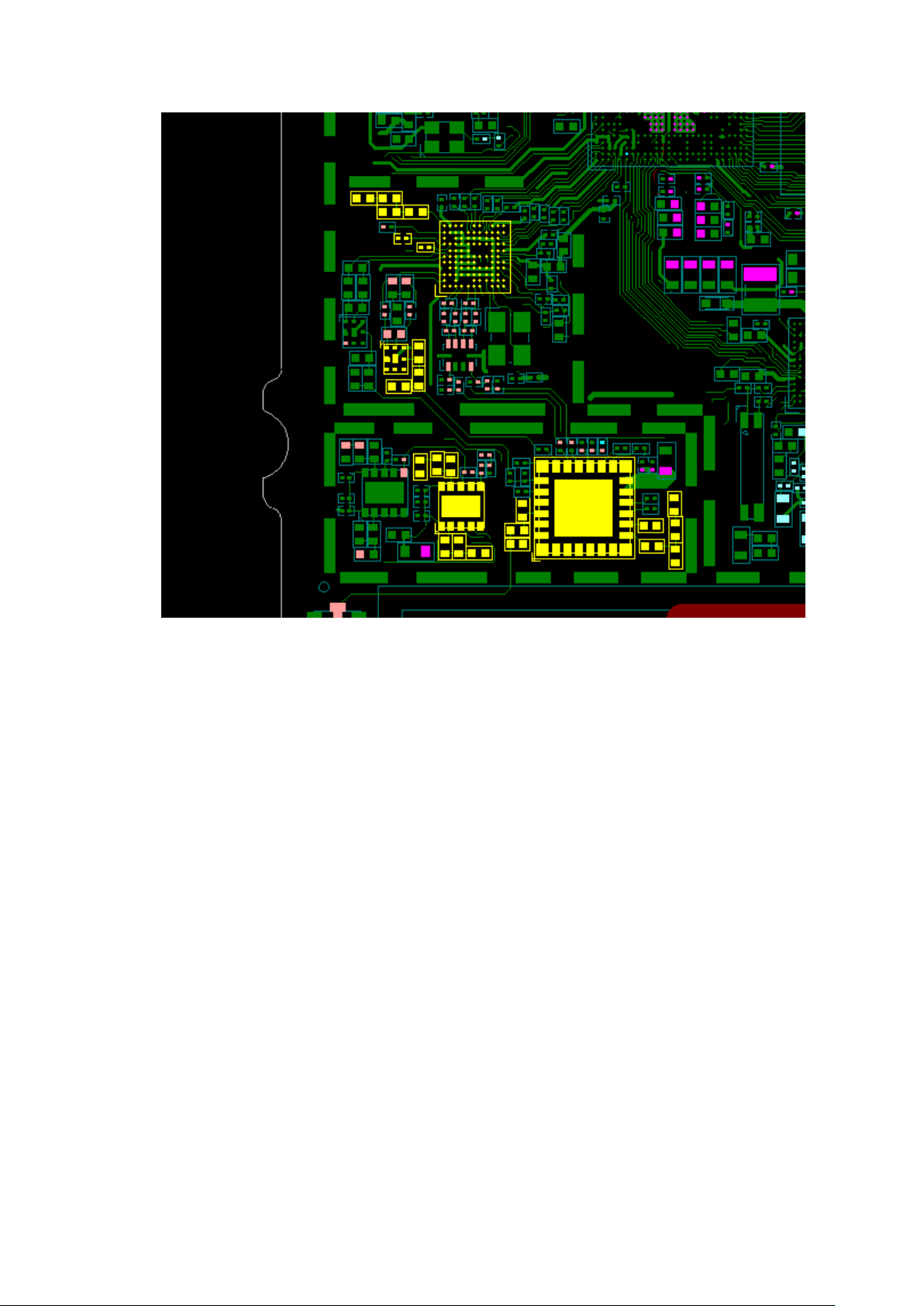
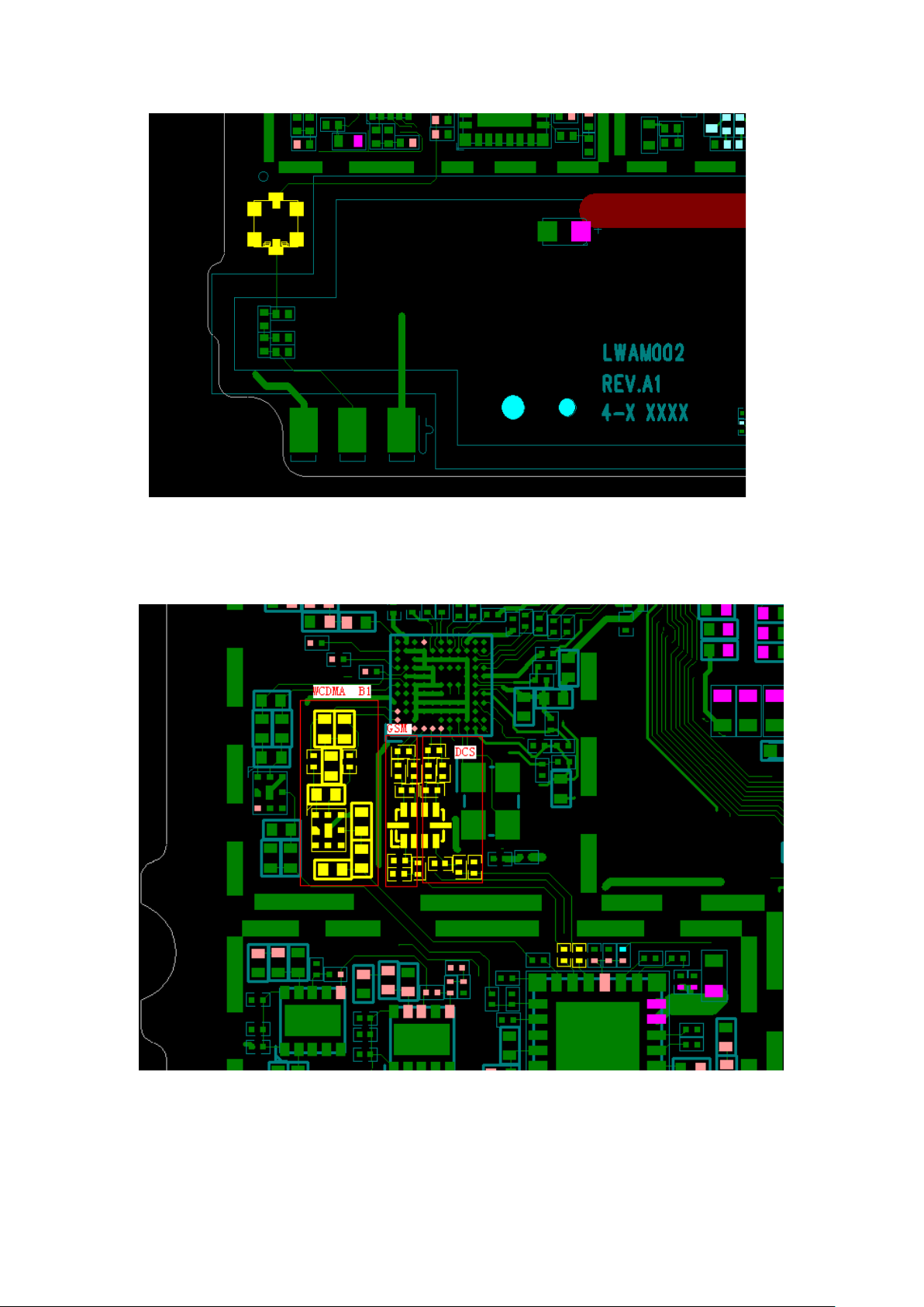
1.3 Mainboard component distribution diagram ....................................................................... 4
1.4 Main IC Names ................................................................................................................... 7
2. RF .................................................................................................................................................. 7
2.1 RF Overview ....................................................................................................................... 7
2.2 RF part service analysis .................................................................................................... 11
2.2.1 Launch part ............................................................................................................ 11
2.2.2 Receive access ........................................................................................................ 12
3. Baseband section ......................................................................................................................... 15
3.1 Outline ............................................................................................................................... 15
3.2 Common Failure Analysis and Maintenance ........................................................... 17
3.2.1 Power failure Check ............................................................................................... 17
3.2.2 Audio faults ............................................................................................................ 19
3.2.3 USB serial port malfunction ................................................................................... 23
3.2.4 LCD Fault .............................................................................................................. 23
3.2.5 FM .......................................................................................................................... 24
3.2.6 Bluetooth and wifi .................................................................................................. 25
3.2.7 Camera fault ........................................................................................................... 26
3.2.8 SIM card failure ..................................................................................................... 27
3.2.9 Motor test is invalid ............................................................................................... 27
3.2.10 Triaxial Gsensor ................................................................................................... 28
3.2.11 T-Flash fault.......................................................................................................... 29
3.2.12Touch Panel function ............................................................................................. 30
3.2.13Distance sensor fault ............................................................................................. 31
3.2.14 Cannot boot failure ............................................................................................... 31
3.2.15 Auto Powe r On ..................................................................................................... 32
Page 3

3
1. PAP3400DUO overview
1.1 PAP3400DUO brief introduction
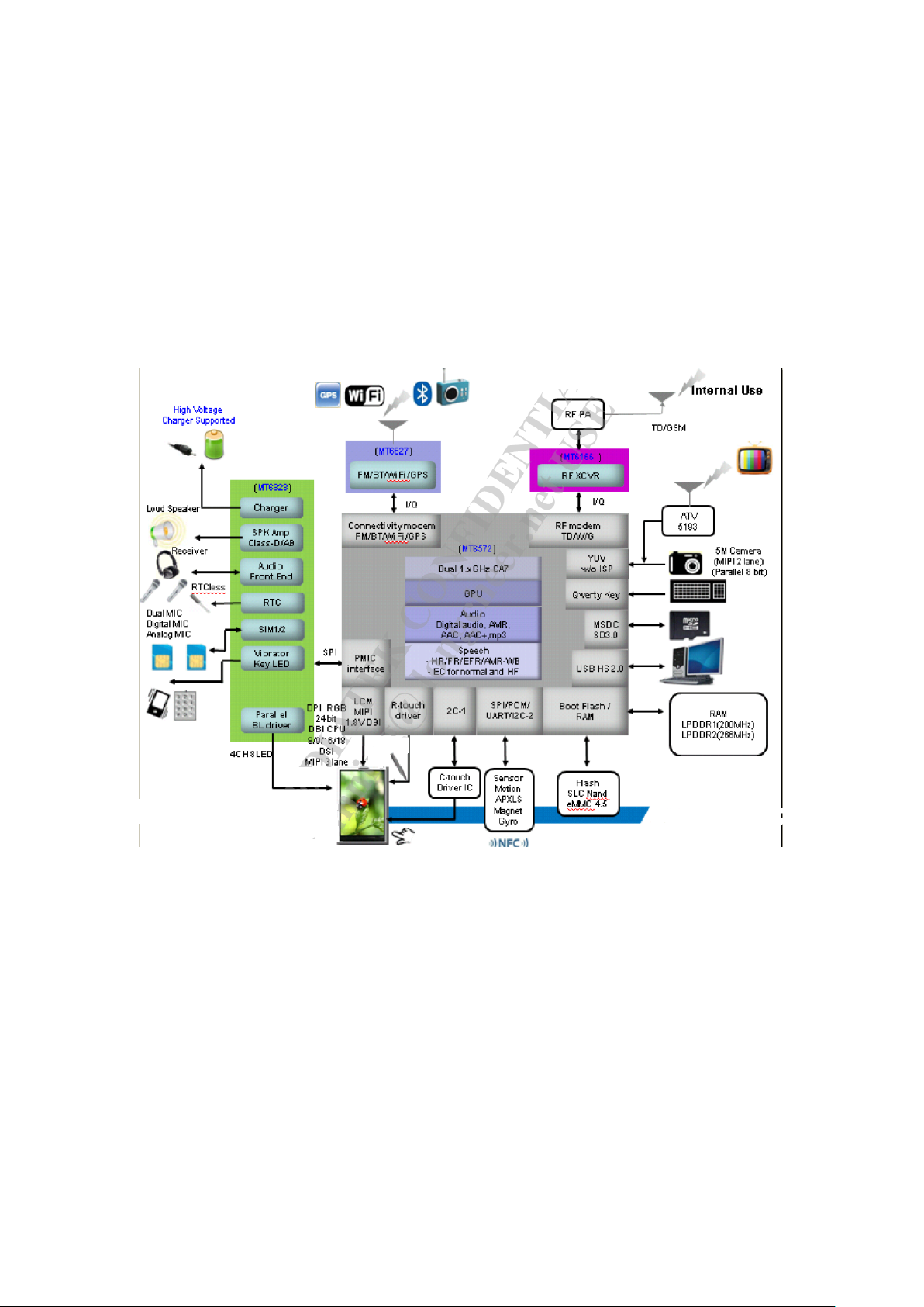
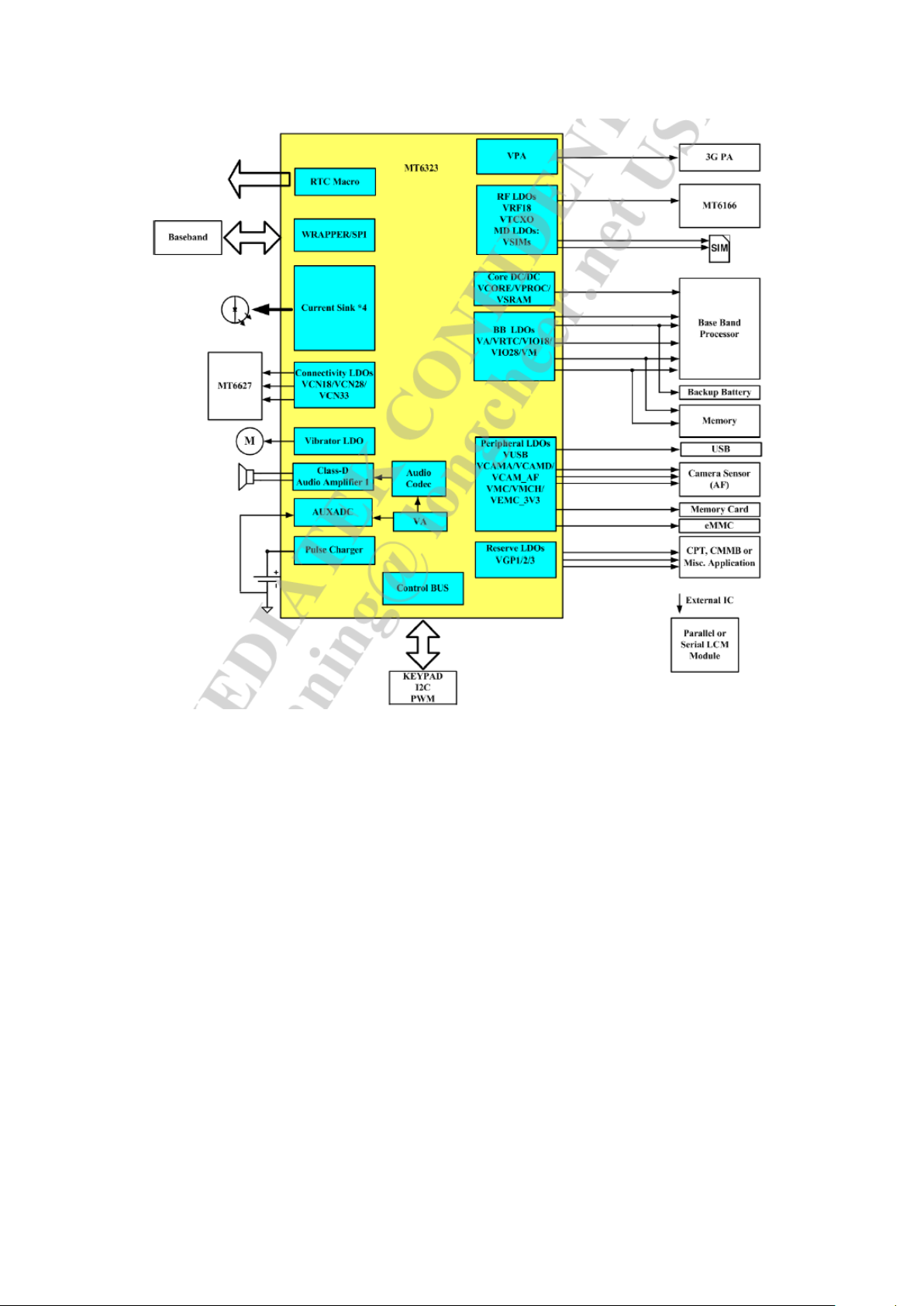
The development and design of the PAP3400DUO PCBA is based on MTK MT6572
platform. The mainboard system mainly consists of the chip
MT6572A/W+MT6166A+MT6323A, which are responsible for t hree part functions, namely,
baseband, radio frequency and power management chip. PAP3400DUO PCBA is an all-in-one
phone mainboard, w hich supports GSM, WCDMA, and covers Bluetooth, WIFI, Camera, FM
functions, GSensor and so forth.
The maintenance of mainboard is one of the important links among mobile products
rear-end producing. The speed and quality of maintenance relate to the rate of good products,
production efficie ncy, and cost control throug hout the pr oducing. In the case of a reasonable
design of product, in the end-producing, finding the significant proportion in the bad board
should be SMT bad and component incoming material ba d. So, whe n maintaining, first, start
with the two aspects. The principal means of fault diagnosis are: (1) find that bad welding spots
or components b y microscopic examination and visua l inspection; (2) guess fail ure positions
from the fault phenomena; (3) confirm the fault units by signal detection.
Page 4
4
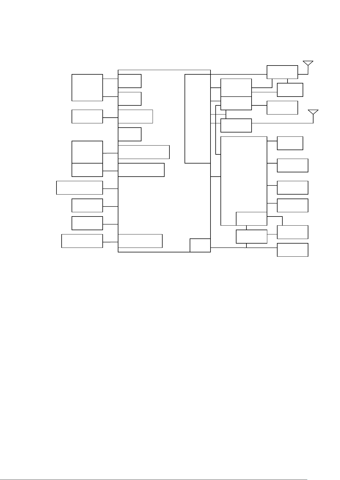
1.2 Function diagram
EMI
SPI
CAM(parallel)
LCD(MIPI)
JTAG、UART
USB
LCD
CTP
Keypad
Debug port
MT6166
FEM
Filter
26M
Charge
VIB
Memory
MCP
TF
Back
CAM
三轴 Gsensor
NFI
MSDC1
MT6572
ABB
26M
MT6627
MT6323
BJT
32K
Audio
SIM
BAT
1.3 Mainboard component distribution diagram
Mainboard TOP
USB
Page 5
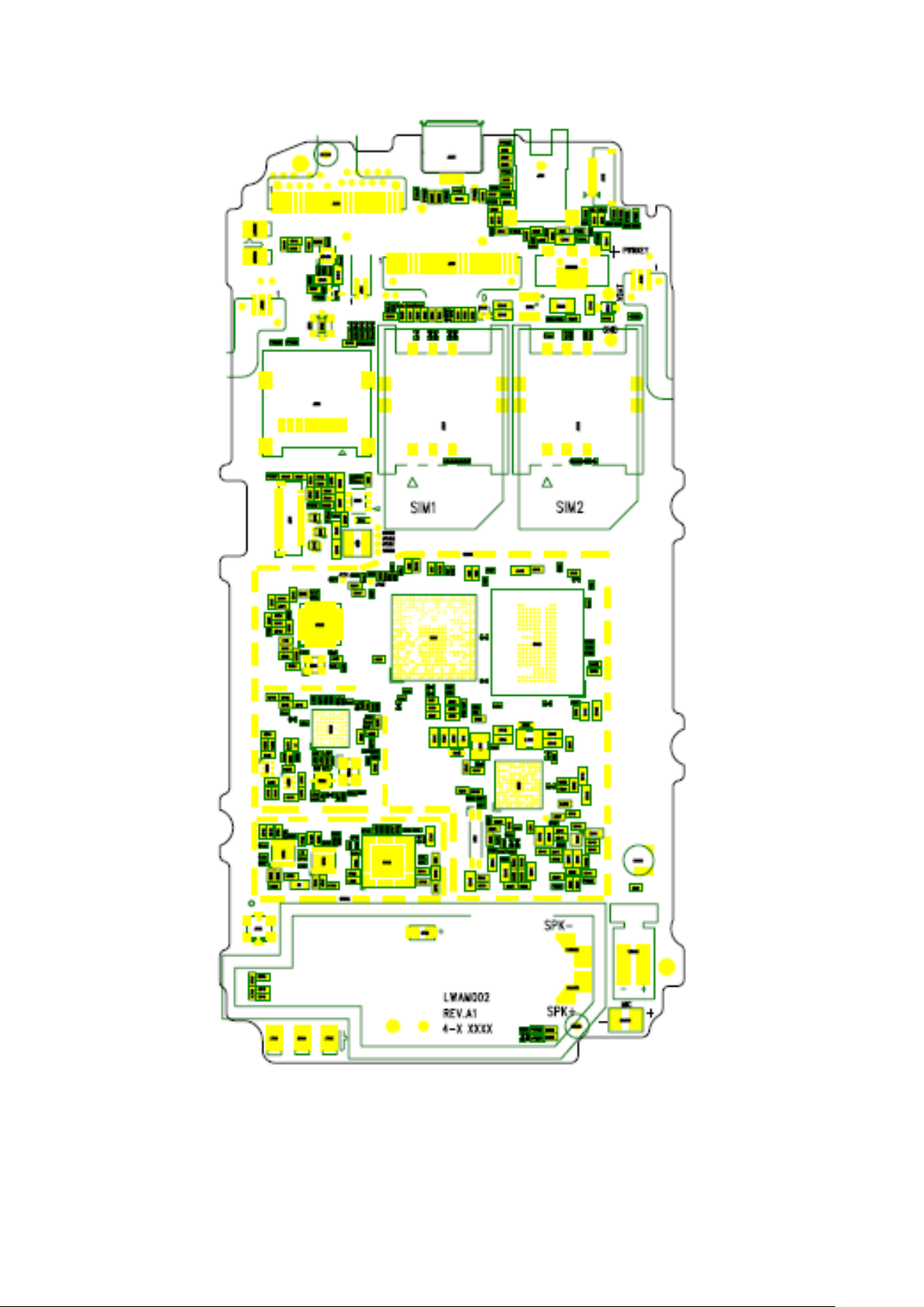
5
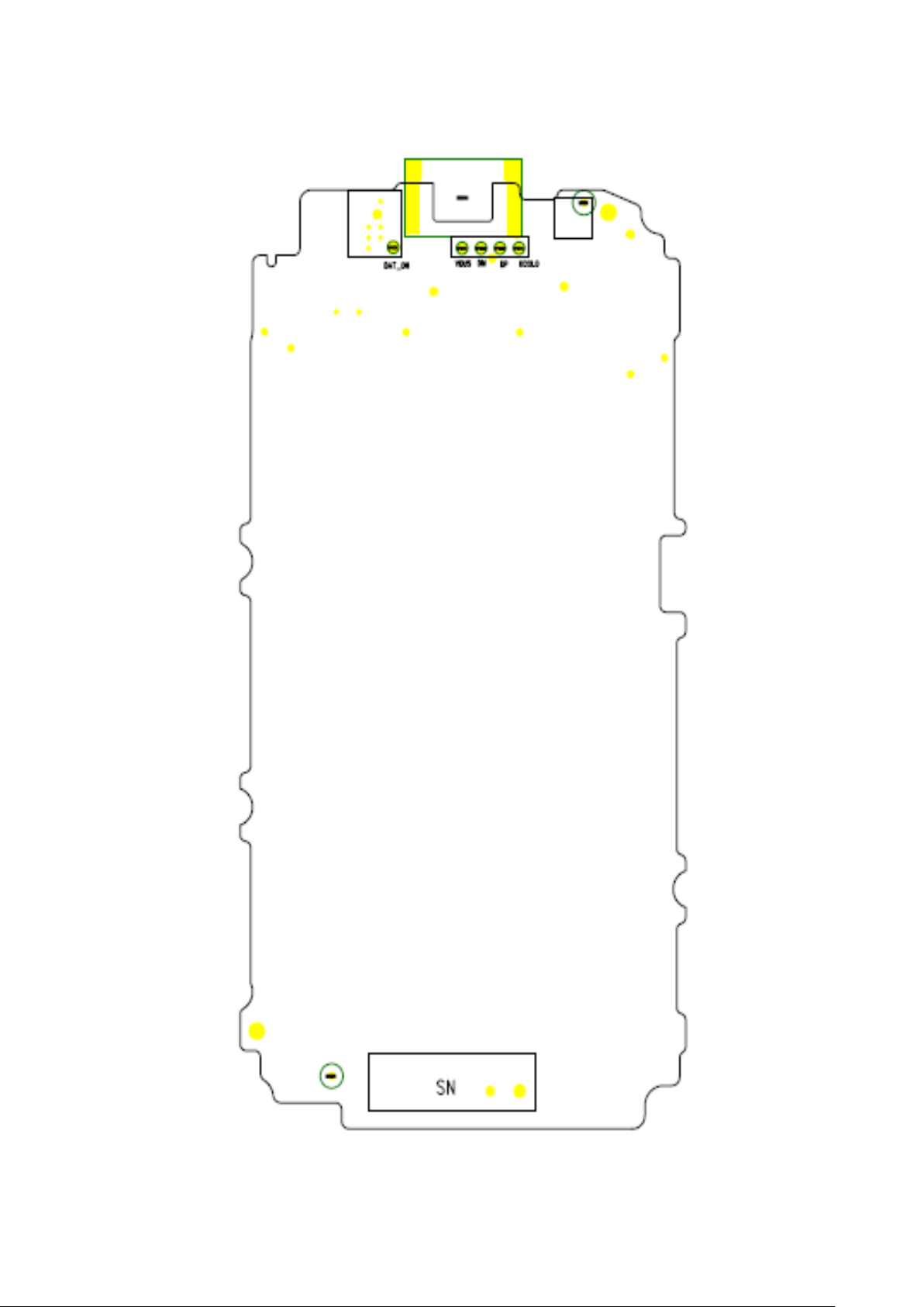
Mainboard BOTTOM
Page 6
6
Page 7
7
1.4 Main IC Names
IC,MT6572W,GSM/EDGE/WCDMA/HSDPA/HSUPA BB+AP
CHIP,1.3G,DC1318
IC,MT6323,Power Management Unit MT6323A U301
MT6572A/W U101
IC,MT6166,TD-SCDMA/HSDPA and GSM/GPRS/EDGE
dual-mode Transceiver
IC,eMMC+LPDDR2,4GB+4Gb,1.8V/3.3V,x8/x32,19ns,TLC KMN5U000ZM-B203 U402
IC,MT6627N,WIFI/BT/FM/GPS 4 in 1 MT6627N U800
IC,SY7301,40V Step-Up LED Driver, PWM control SY7301ADC U801
IC,HRPF88183B,PA+4*TRX WCDMA ASM,Tx-Rx FEM for
Quad-Band GSM/GPRS
IC,SKY77761,RF PA Module,LTE Band1/CDMA
IMT,1920-1980MHz,3x3
TRANS,PNP,30V,3A WPT2F30 U303
MOSFET,N-Channel,-40V,-180mA,4.5Ω PNM723T703E0-2 U305
Schottky diode 1PS79SB30,115 D301,D302,D801
DIODE,ZENER,5.1V,500mW PZ3D4V2H D305
32.768KHz Crystal
26MHzCrystal(3225) X1E000021043400 X600
X-CAP,3.3V,0.01mAh,Φ3.8,1.5H XH311HG IV07E GB301
MT6166A//MT6166V U600
HRPF88183B U700
SKY77761 U703
Q13MC1461000200//
Q13MC1462000200
X301
IC,MC3430,3-Axis Acceleration Sensor,Digital,8bit MC3430-I5 U1400
FILTER,BALUN,GSM,GSM850/PCS1900 OR
EGSM900/DCS1800,2012
DUPLEXER,WCDMA BAND1,
1950MHZ/2140MHZ,BALANCED,2016
RFBLN2012090BM5T25 U602
PJ D6PE2G140P3AW-Z U609
2. RF
2.1 RF Overview
MT6166 is MTK's multi-mode and multi-frequency transceiver chip, supporting GSM/
GPRS/EDGE, WCDMA dual-band mobile phone.
The circuit description of Receiving part
Page 8
8
Receiving part functional block diagram
It can be seen from the schematic diagram, first, signal is received through antenna, reach RF
coaxial switch (J700) through antenna matching, and then enter RF PA module U700.
Choose GSM signal through PA module (U700) inner switch, output from PIN20, into receiving
filter U602, passing matching circuit, into MT6166 U600’s C1&D1 port, into MT6166 (U600)
inner LNA;
Choose DCS signal through PA module (U700) inner switch, output from PIN19, into BALUN
FILTER U602, passing matching circuit, into MT6166 U600’s E1&F1 port, into MT6166 (U600)
inner LNA;
Page 9
9
Choose WCDMA B1 signal through PA module(U700) inner switch, output into antenna
diplexer (BAND1-single-end RX) U609, divided into TX and RX two ways. RX passes the match,
into MT6166 U600’ A2&A3 port, into the inner LNA.
The each ways’ signal above pass the inner down-conversion, amplification, and after ADC
converting, into baseband.
The description of transmit part
Transmit part is the other way around,
GSM baseband signal within passes up-conversion and amplification, then output from
U600.A11, through outputting and matching, into PA module U700’ PIN10, through signal
amplification, and output into antenna port.
Page 10
10
DCS/TD(A/F) baseband signal within passes up-conversion and amplification, then output
from U600.B8, through outputting and matching, into PA module U700’ PIN9, through signal
amplification, and output into antenna port.
WCDMA B1 baseband signal within passes up-conversion and amplification, then output
from U600.A8, passes matching circuit into WCDMA power amplifier. The power amplifier has
in-built coupler, can coupling one part of signal to MT6166, to detect output signal. After PA
signal amplification, output to the PA module(U700)inner switch, TX’s input foot, and then
outputs to antenna transmit.
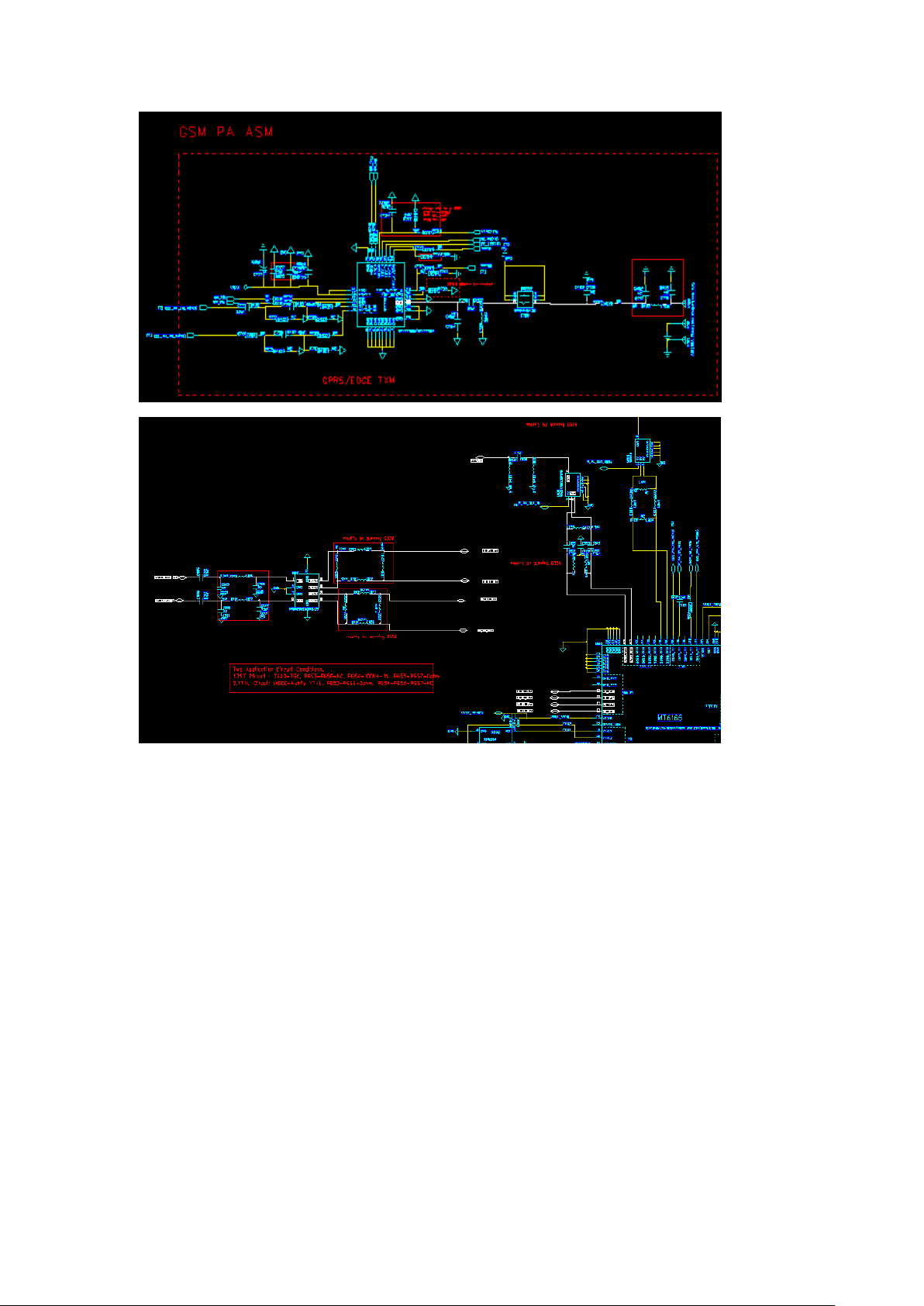
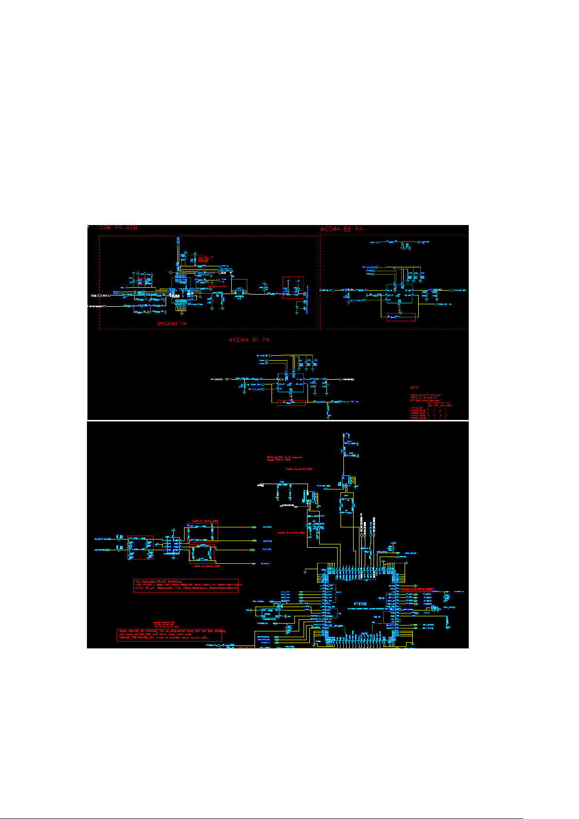
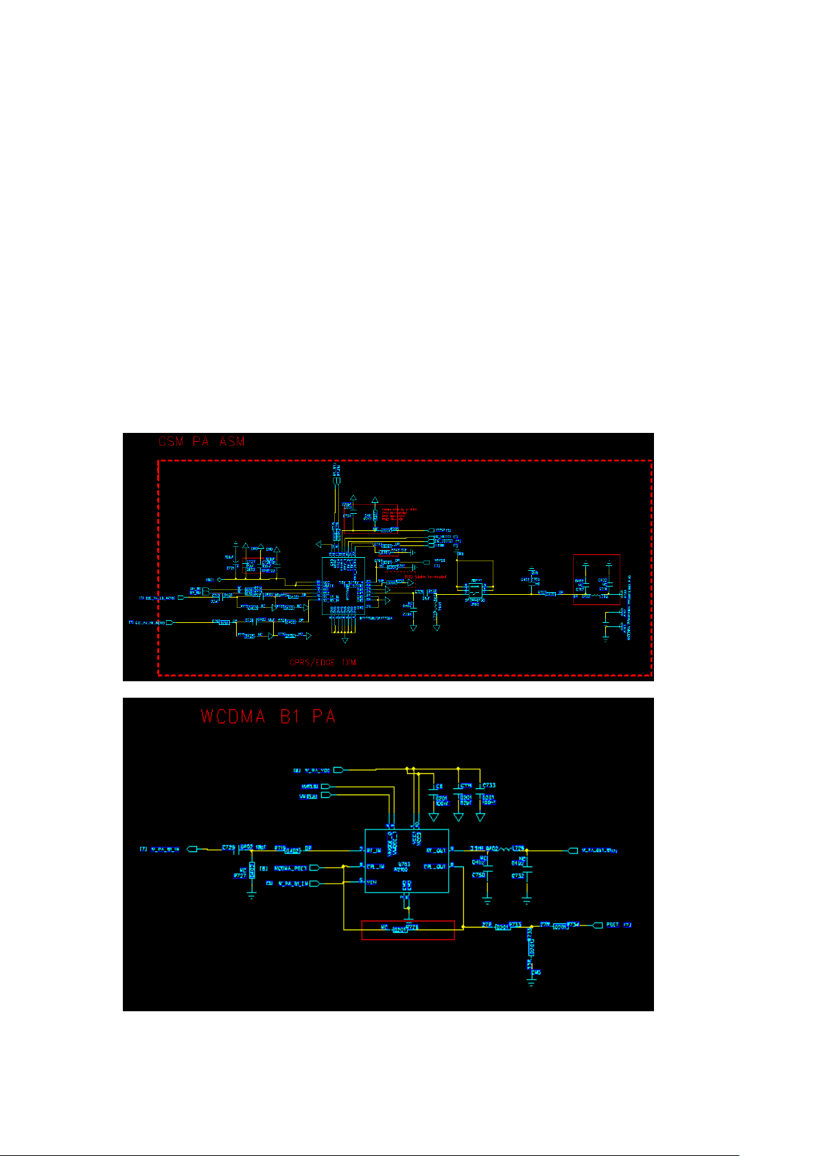
PA introduction
PA:HRPF88183B supports 2G four-band, the phone supports GSM/DCS two bands.
SKY77761 supports WCDMA’s BAND1
Page 11
11
2.2 RF part service analysis
2.2.1 Launch part
Test conditions 1:Vbatt=3.8v~4.2v
Test Equipment
Agilent8960, oscilloscope, frequency spectrograph, voltage-stabilized power,
multimeter
If BT, F T find output power low or no power output, can follow the order below to
check launch access by using multimeter, and also can choose middle some grade
to confirm whether its front grade or rear grade has problems.
GSM/WCDMA Launch
1、 To check whether the RF test socket J700 is welded well b y visual inspection? Whether
the female polarity is correct? Whether the center of the female seat has foreign matter?
2、 To check whether the components of U700&U703&600&U609 transmit circuit are
patched abnormal by visual inspection
Page 12
12
3、 If the visual inspections above have no abnormality, replace U700(for 2G&3G) test
4、 If has no improvement by replacing U700, replace the U600(for 2G&3G) test
5、 If remains no improvement, replace the U703(for 3G) test
6、 If remains no improvement, replace the U609(for 3G) test
2.2.2 Receive access
Can follow the procedure below to check
1、 To check whether the RF test socket J700 be welded well by visual inspection? Female
polarity is correct? The center of the female has foreign body?
Page 13
13
2、 Whether filter U602(for 2G)&U609(for 3G) on the receive path, and matching circuit
welded well?
Page 14
14
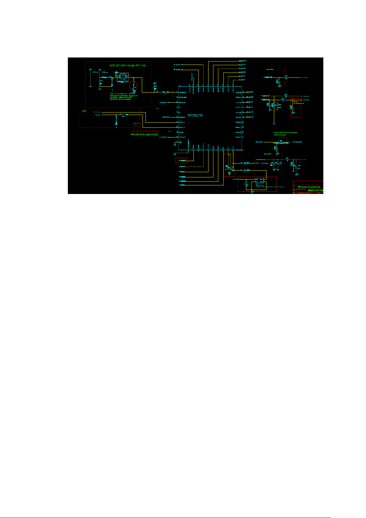
WiFi/BT/FM Part
WIFI and BT share RF access, signal is entered by antenna. The clock uses 26M clock
provided separately. Data transfer interface and audio interface are directly connected to the CPU.
WIFI main problems:
1. MT6627 chip has been calibrated before out of factory, production line directly do FT test.
The probability that it appears problems by WiFi test is ve ry low, the FT failure problems,
please power off and restart the phone, first retest.
2. WIFI test EVM fail. This major and power, as well as the freq error, if the power is too high
or the freq too big EVM may also lead to excessive, please re-test.
3. WIFI RX fail, main receiving sensitivit y fai ls to pass, Generally, production line testing has
not shielded box, RX vulnerable to external signal interference, If come across such problems,
can change the channel to do the test.
Bluetooth main problem:
Bluetooth does not need calibration, only need to check the function, if unable to search the
device or Bluetooth cannot be opened, check whether the J800 is welding bad or body bad.
Page 15
15
3. Baseband section
3.1 Outline
Baseband circuit completes main functions: the procedure data storage, keyboard
input, and the communication between the RF module, RF power control, the control
of the power management module, RUIM card interface, serial download interface,
Camera, T-flash, G-Sensor, and MMI (man-machine interface, such as the display,
backlight, buzzer, speaker, microphone, motors, etc.).
3.1.1 Memory
The baseband part has an eMMC+LPDDR2 MCP. Wherein the amount of eMMC storage
4Gb, it stores a communication protocol layer and application layer software, and
storing various system parameters, calibration parameters, such as RF control
correction value of an audio signal, the IMEI number, and other important information
and store user settings data such as phone number, CALL volume, and tone; LPDDR memory
512MB, temporary variables stored phone program run。
3.1.2 Power Management
Page 16
16
PMU chip is MT6323,which contains 3 DC-DC and 23 LDO, one 0. 7W class D audio
frequency power ampl ifier, 4-way current sink, SIM card level shift, and s o on.
3.1.3 Battery
1500mAh 3.7V lithium-ion battery.
3.1.4 32KHzCrystal
32KHz crystal is used for power-saving mode and real-time clock.
MT6572 platform supports 32K-less mode, PAP3400DUO does not adopt at present.
3.1.5 SIM Card
SIM card level shift integrates in MT6323, card 1 supports WCDMA and GSM dual modes.
3.1.6 Audio frequency
The largest impedance is 2.2KΩ.
Headset as a standard 3.5mm jack port, the nominal resistance 32Ω.
Speaker adopts 2014 specification, Receiver adopts 1506 specification.
3.1.7 I/O Interface
I/O Connector MICRO USB interface standard. Mainly used for software, download
Page 17

17
picture messages.
3.1.8 Display
The main screen is 4.0 TFT color screen 480*800(WVGA).
3.2 Common Failure Analysis and Maintenance
Before cutting board after the completion of the production line SMT X-RAY inspection,
according to the actual situation, X-RAY examination cannot be found 100% badness, X-RAY
inspection may omissions some fault plate flow down. If found fault plate in the testing process,
the first step is to re-check of the X-RAY and carefully to see if there is even welding, lap welding,
Weld, if normal, analyze the situation following the positioning。
3.2.1 Power failure Check
The failure phenomenon caused by a power failure: cannot boot, shutdown leakage current boot
large current.
The main reason for the problem: Weld, electrical the original filtering or ESD device to
short-circuit, burning with the device is connected to a power source.
Positioning as well as steps to solve this type of problem is as follows:
1, Troubleshoot and connected to the power supply components of the welding, Weld, or the
peripheral devices even tin.
2, with a multimeter rule out whether there is power to short-circuit, and step by step to
troubleshoot the cause of the short (mainly: even tin, IC burned ESD protection device
breakdown, capacitor breakdown).
3, boot to test the power output is normal.
If a power output value is not normal, whether the view filter capacitor welding problems,
whether the breakdown, filter capacitor is broken, replace; excluded one by one, and finally you
can navigate to the main chip damage.
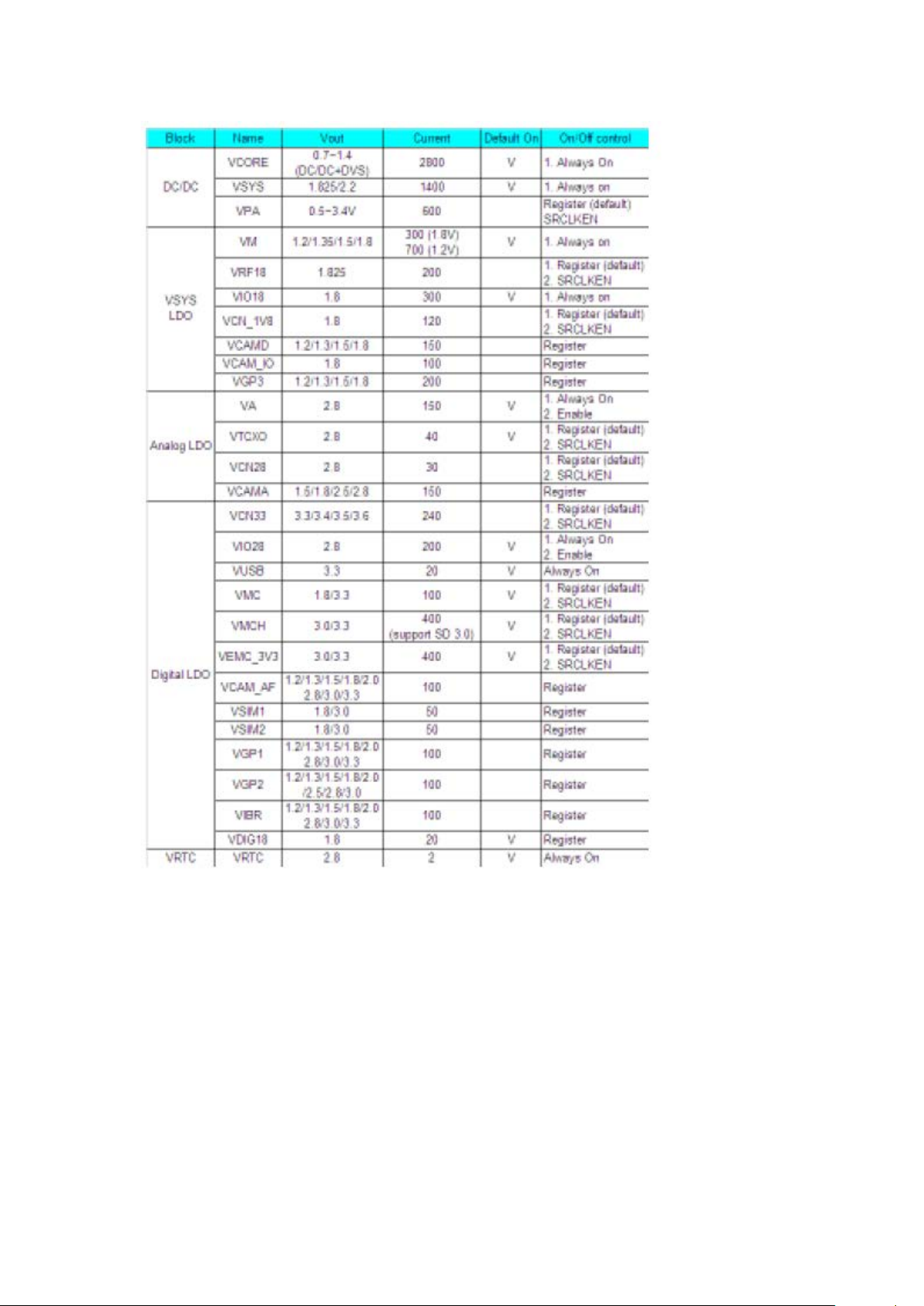
Each the power test position and the normal boot value is shown in the following table
power
VPROC_PMU for BB VCCK,VCCK_CPU
VSYS_PMU for PMU AVDD22_BUCK
VA_PMU for PMU AVDD28_ABB,AVDD28_AUXADC
VCN_2V8_PMU for 4 in 1
VTCXO_PMU for BB AVDD28_DAC,for MT6166
VCAMA_PMU for cam AVDD 2.8V
VRTC for back up bat
Page 18

18
VM_PMU for BB VCCIO_EMI,for memory
VRF18_PMU for MT6166
VIO18_PMU for 1.8V PERIPHERAL
VIO28_PMU for 2.8V PERIPHERAL
VCN_1V8_PMU for 4 in 1
VCAMD_PMU for cam DVDD 1.8V
VCAMD_IO_PMU for cam DOVDD 1.8V
VEMC_3V3_PMU /
VMC_PMU for BB DVDD3_MC1
VMCH_PMU for TF card
VUSB_PMU for BB AVDD33_USB
VSIM1_PMU for SIM1
VSIM2_PMU for SIM2
CTP_2.8V_PMU for CTP 2.8V
VIBR_PMU for VIBR
VGP2 /
CTP_1.8V_PMU for CTP 1.8V
Page 19
19
3.2.2 Audio faults
The audio part has main four parts including the speaker, receiver, mic and
headphone. First undesirable phenomena distinguish what part of the problem, and
then analyzed according to the following respective module.
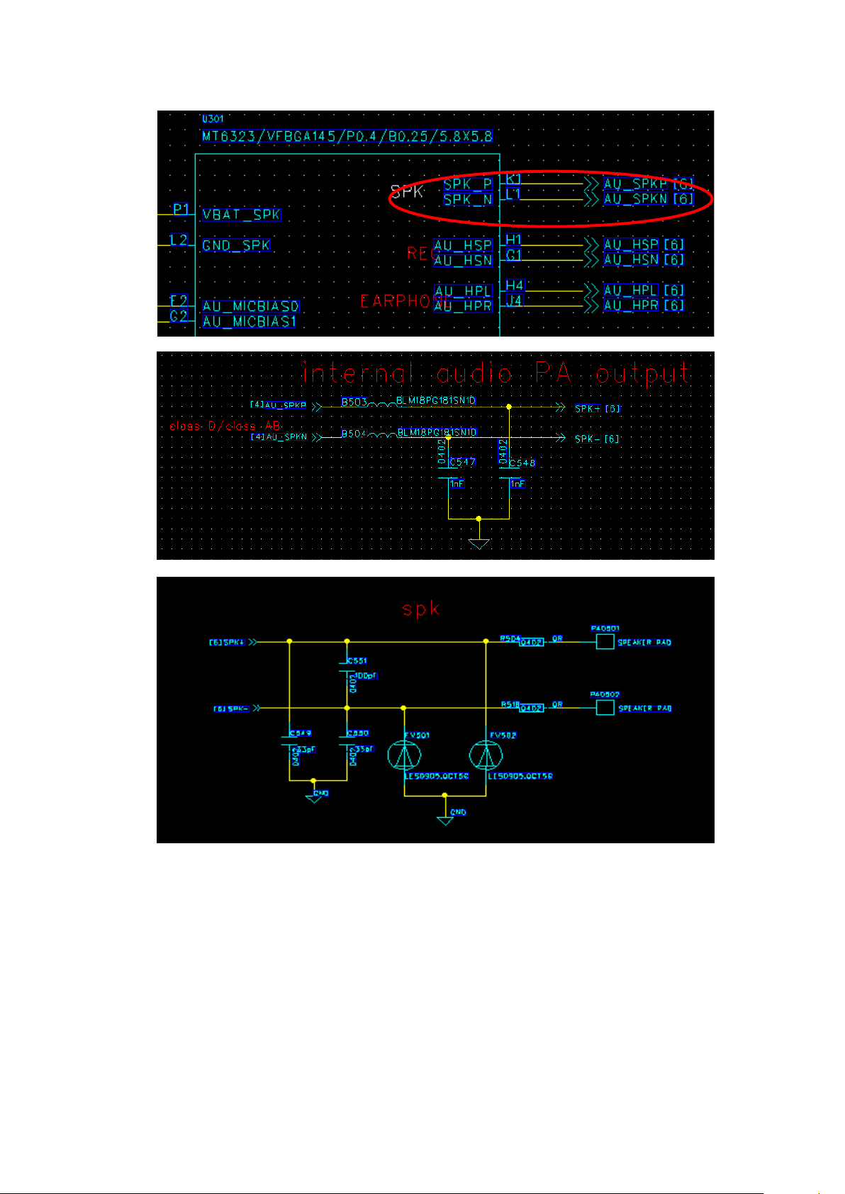
(1)Speaker loop
The PAP3400DUO phone’s speaker circuit is as follo w. Speaker audio output diagram is
as follows:
Page 20
20
Speaker Common faults and reasons:
1, SPK Ringtones reasons: 1) light board, SPK itself is bad, or the connection FPC
problem, the whole observation board board PFC Cartridge is skew, not in
place 2) B503、B504、R504、R518 relevant component there is dry welding 3 )
software problems
2: SPK ringtones or murmur: 1) software volume settings 2) SPK ontology reasons
Page 21
21
3. Switch machine ringtones, but engineering tests SPK OK: 1) scene mode is set to switch
machine ringer off 2) software problems, itself boot ringtones;
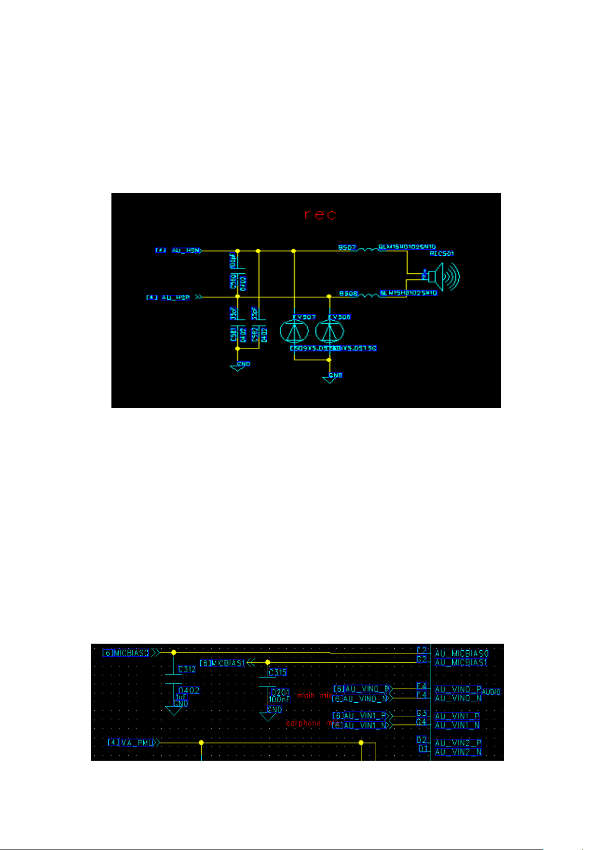
(2) Receiver circuit
PAP3400DUO phone receiver is embedded in the mobile phone front shell through shrapnel
and motherboard connection. Mainly used for the call. Receiver circuit diagram as shown below.
Receive Loop
Receiver Common faults and reasons:
1, Receiver without sound: 1) Receiver assembly adverse, the shrapnel and board
poor contact 2) Receive ontology bad 3) the volume settings or software problems
2, Receiver noise or volume: 1) Receiver incoming material, whether caused by
pad short circuit 2) relevant components have solder skips 3) software problems
(3) Mic loop
The PAP3400DUO contains two MIC circuits, the main MIC and headphone MIC. The main
MIC was inserted needle. Loop schematic diagram as following:
Main MIC common faults and causes
1 MIC unable to send words or recording: 1) MIC poor welding 2) MIC body bad
2 MIC noise or sound: 1) MIC ontology bad 2) software problems.
Page 22
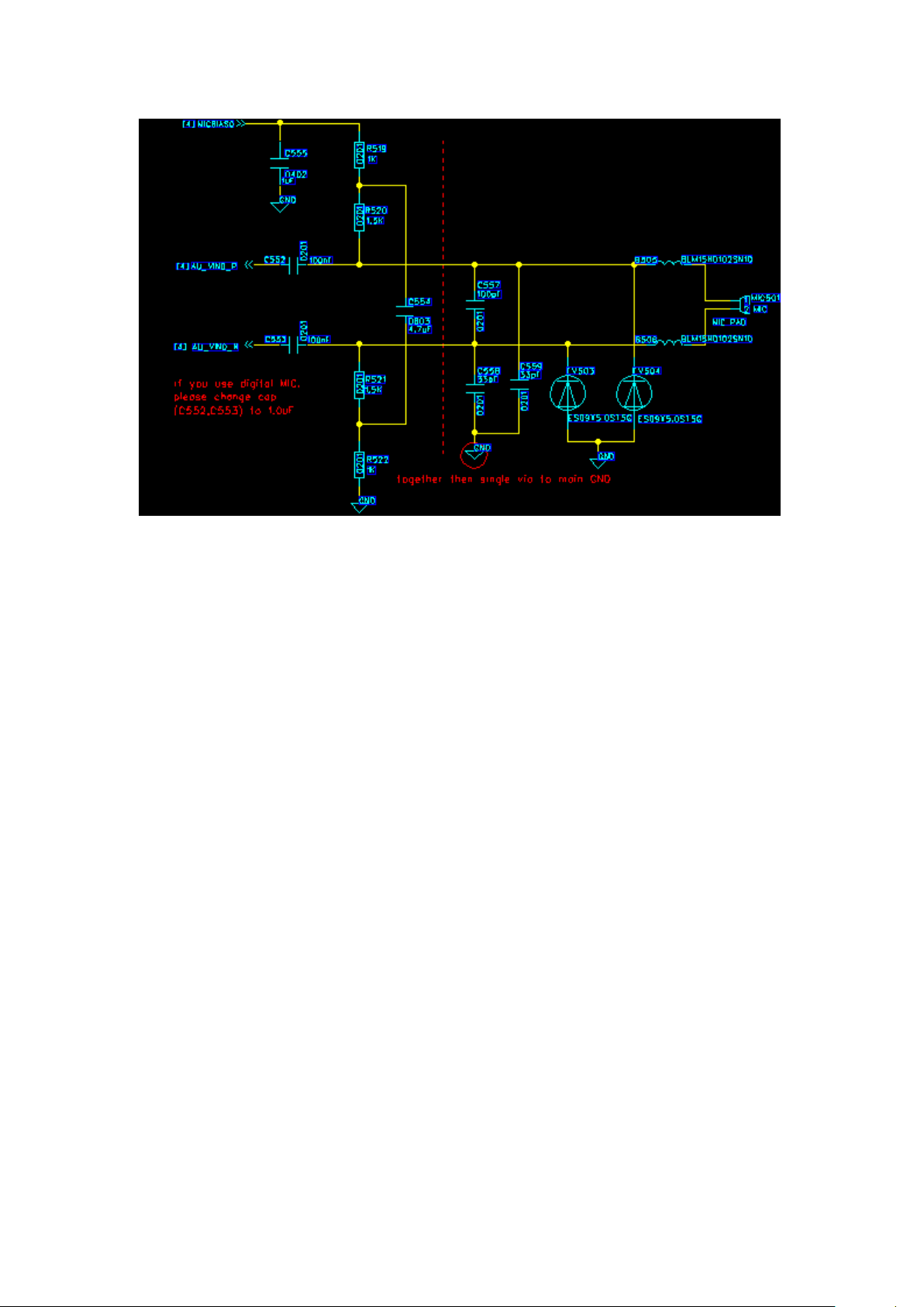
22
Main MIC
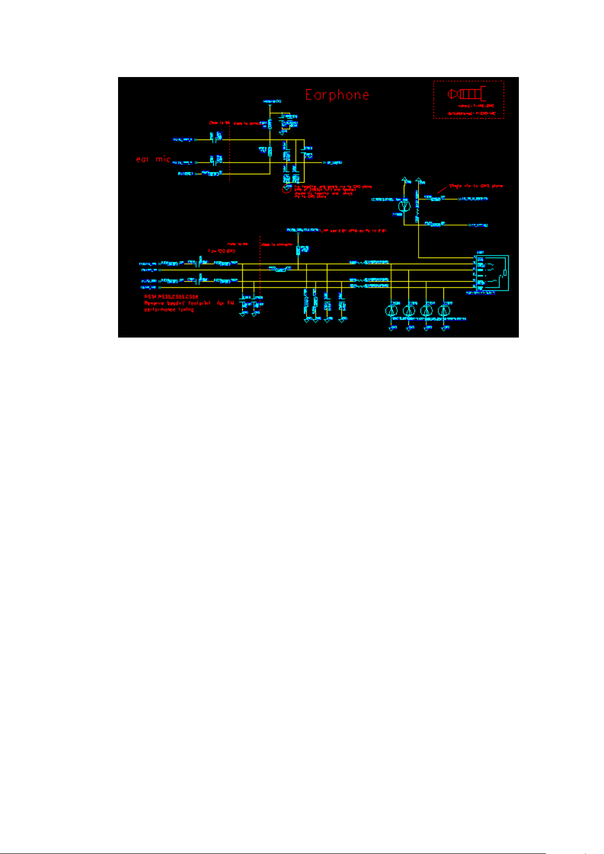
(4)Headphone loop
PAP3400DUO phone use headphones with a standard 3.5mm headphone. Its circuit
diagram is as follows:
Headphones common faults and reasons:
1, headphones only one channel sound: 1) the headset is not inserted in place 2) R534、
R535、C503、C504、R532、R533、B509、B510 Relevant component Weld. 3) R528、
R529、C501、C502、FV509、FV511 Relevant component breakdown shorted to ground;
2 headphone left and right channels are no sound: 1) the headset is not inserted in place 2)
Relevant component breakdown on the short circuit;
3, unplug the headphones bank borrowing does not recognize: 1) R530、R531 Relevant
component Weld; 2) whether headphones Block shrapnel and motherboard good contact 3)
software reasons
4 headset MIC no transmitter: 1) the headset is not inserted in place 2) B511、C565、R524、
R525、C563、C564 Relevant component Weld 3) FV512、C567、C568 Relevant component
breakdown on short-circuit;
Page 23
23
Headset MIC AND 3.5mmHeadphone jack circuit
3.2.3 USB serial port malfunction
During the test, "open serial port failure" will often occur. Main reasons are:
1) phone is unable to power on, Please refer to the fail to power on malfunction
maintenance
2) USB test points are oxidized, not contacting with fixture well
3) USB connectors J1001 is bad welding
4) USB circuit problems
3.2.4 LCD Fault
PAP3400DUO adopts 4.0-inch TFT LCD, The part of the circuit schematic as shown below.
Common problems and causes of the LCD module:
1, LCD screen is blank. 1) LCD is not installed or and fixture poor contact)
LCD backlight circuit is bad, check backlight so that the foot is pulled, check
whether welding problems 3) LCD itself fault.
Page 24

24
2, LCD blurred screen and white screen. Description LCD backlight circuit OK, just
shows abnormal. The cause of the malfunction is usually: 1) LCD connector poor
contact, poor welding and fixture poor contact 2) related components Weld or even
tin short circuit 3) software problems
3. LCD black spots, bright spots, black lines, stripes Failure: LCD ontology bad.
3.2.5 FM
When FM is working, should insert headphone as its antenna. FM outputs audio
signal to the CPU Codec, ampl ify playing or record. FM common faults and causes:
1, FM cannot search frequency or less frequency reason: 1) headphone without
Page 25

25
inserting or not insert goo d 2) sur r ounding environment is bad, such as plant, garage, etc.
FM signals itself is weak or no FM signals source 3) FM antenna circuit exists poor
soldering or short circuit, lead to unable to receive FM signals or FM signals leak 4)
software reason
2,FM without sound reasons or murmur 1) this FM radio frequency is invalid 2) FM
weak si gnal 3)related component bad-welding 4) headphone
whether headphone s ocket s hrapnel cont acts with t he m ainboard wel l 6) wheth er headph one
socket welding is OK
3,FM module operation failed. 1)Check whether the I2C and CL K signal ar e nor mal
or not 2)Software fault
was not put in place; 5)
3.2.6 Bluetooth and wifi PAP3400DUO BT and wifi adopt MT6627 chip. Data transfer interface and audio
interface are directly connected to the CPU. Common failures are:
1, Bluetooth function failure, you need to check the Bluetooth is turned on, the
Bluetooth Visibility settings are correct. The Bluetooth power supply and clock circuit
the existence of the phenomenon of short circuit or Weld.
2, Bluetooth effective distance is short, easily disconnected. Need to check
whether Bluetooth antenna circuit soldered or short circuit, Bluetooth antenna and
motherboard contact well.
Page 26

26
3.2.7 Camera fault
Camera common fault and why:
1, Camera initialization failed, could not enter the Camera the main interface. 1) Camera poor
welding or poor contact 2) the Camera Ontology failure 3) Camera Power supply is not normal
(Weld, or short-circuit led to) 4) related components welding problems
2, Camera Preview shows blurred screen or color is not normal. 1) Camera poor welding or
poor contact. 2) related components welding
Page 27

27
3.2.8 SIM card failure
PAP3400DUO SIM card module circuit is connected directly with PMU through four-path signal
from SIM slot. The major failure of the module does not know the card, the reason usually: 1)
SIM card GSM card and SIM deck poor contact 2) poor SIM card socket welding 3) software
problem cause the phone to pick a card, change the card to confirm. 4) SIM card holder exist Weld;
5) card exceeds the itinerary or inserted upside.
3.2.9 Motor test is invalid
PAP3400DUO adopts columnar motor, with simple circuit. As shown below. Common motor
failures and the reasons are:
1, the motor without vibration 1) motor and motherboard contacted poor
2, the motor was felt as weak 1) motor ontology bad) the cause of the software settings
3 motor vibration sometimes 1) motor and motherboard poor contact
Page 28

28
3.2.10 T riaxial Gsensor
PAP3400DUO triaxial GSensor circuit is provided power by VGSENSOR_PMU, supply
voltage 2.8V,1.8V I2C is imitated by GPIO. Triaxial GSensor common faults and reason:
1, Sensor sensitivity is low, response is slow: Software problems.
2, Triaxial GSensor function NG, check whether Triaxial GSensor module circuit has
welding or short-circuit faul t .
Page 29

29
3.2.11 T-Flash fault
PAP3400DUO T - Flash circuit is connected with CPU through the special SDIO bus, circuit
diagram shown below. T - Flash the common faults and reasons are:
1, T–Flash read-write test is failure. 1) T - flash for fault card or and T kaka seat have had no
contact with good 2) below the resistance there may be short circuit, or virtual welding
phenomenon. Capacitance may on short circuit. (using a multimeter to test whether T card signal
and ground and VMCH short circuit can eliminate) 3) software reason
2, T card not to know card: T holder PIN feet virtual welding, on MLV welding reverse and
capacitance breakdown
3, T - Flash can't through the USB for transmission. 1) T - Flash itself, speaking, reading and
writing test failure fault 2) software fault 3) USB fault
Page 30

30
T card circuit
3.2.12Touch Panel function
Touch Panel common fault and reasons are:
1. TP sensitivity low, slow reaction: software problem;
2. Touch Panel function NG, at present is mainly due to FPC itself partial long cause, the I2C
initialization failed;
TP circuit
Page 31

31
3.2.13Distance sensor fault
PAP3400DUO distance sensor is realized through the TP. During the call, when a certain
superficial TP sensor has reaction, realize off- screen app, etc.. If no reaction, should check
whether the TP firmware is the newest and has any problems or not.
3.2.14 Cannot boot failure
Can't boot failure is the phone fault with highest probability of occurrence. Software
problems, welding problem, device failure is the main factor causing failing to boot. Maintenance
process can cooperate with LCD and startup current, as well as the keyboard and so on to orientate
approximately.
1, Power off leak current is large. The main failure reason is VBAT connected components
had to earth short circuit problem. Usually radio frequency PA burned or welding problem cause.
The simpler method is looking for is a hot devices, general such devices have larger may on short
circuit.
2, Boot without current, LCD no display, keyboard, etc not bright. 1) boot key SMT bad 2)
battery connector bad contact (through the plug charging machines)
3, Crashed when boot, 1)can try to re-download the software, 2)replace memory
4, Current is large when boot. LCD displays normally, even can enter the IDIE interface,
single board is very hot 1) The individual power circuit short circuit to ground phenomenon exists
in the phone, which is usually the problem that ESD protective devices of module circuit
breakdown short circuit to ground or weld problems.
Page 32

32
3.2.15 Auto Power On
1, Connect the power , po w er on, insert USB don't turn on, sof tware decides to need to
connect to the power, and then power on.
2, W hether Power on key has incoming materials problem, whether welding is short
circuit.
Page 33

PAP 3400
service manual
Page 34

content
1、 Product introduce..………..p3-p4
2、 Disassembly guide ……….p5-p17
3
4
、Structure parts diagram…..p18
、 Repairing guide …………...p19-p29
2
Page 35

Product introduce
3
Page 36

Product introduce
Model :
Product size
Platform
Memory
System
Frequency band: WCDMA:900/2100,GSM:900/1800MHz
Battery
charger: Travel charger
USB cable: MICRO 5PIN
earphone
LCD&TP
Camera
: 4GB+512MB (Nand&sdram+RAM)
:Android 4.2
: 1500mAh
:0.3M and 2.0M CMOS
:123×63.5×11.9mm
:MTK6572,dual-core 1.2GHz
: 3.5jack
: 4.0 FWVGA TN, 480*800, Capacitance TP
Support
Support
:BT4.0,WIFI,FM。
:3D graphics accelerator,accelerator sensor
4
Page 37

Disassembly guide
1. Tools list
Tweezer /Cr oss scr ew driver/ Solder/Tommy bar/hot gun
Tommy bar
Tweezer
Cross Screw driver
Solder iron
Hot gun
5
Page 38

Disassembly guide
2. Battery caver disassembly
open the battery cover
,
as the Fig. 1
Battery
cover
Fig. 1
6
Page 39

Disassembly guide
3. Back caver disassembly
1)
Unscrew 10 screws in back cover ,as the Fig.2;
Fig. 2
7
Page 40

Disassembly guide
2) Disassemble back cover with Tommy bar ,as the Fig.3;
Back
cover
SPK
Fig. 3
8
Page 41

Disassembly guide
4.Main board an d front cover di sas sem bly
1)The main components of distribution,as the fig.4;
TP con.
Earphoe
con.
USB con.
Back CAM.
Front
CAM con.
Battery con.
SIM con.
Main PCBA
MIC
T card
con.
LCD con.
Fig.4
9
Page 42

Disassembly guide
2)remove two screws and open the LCD con.& TP con. ,and remove the
volume key FPC & power key FPC as the fig.5;
TPcon.
LCDcon.
Fig.5
10
Page 43

Disassembly guide
3) Disassemble the main board.as the FIG.6
Fig.6
11
Page 44

Disassembly guide
5. Front and Back camera & Flash FPC & Side key FPC & MIC &Camera
bracket disassembly
)disassembly the Camera bracket ,as the fig.7;
1
Fig.7
Camera
bracket
12
Page 45

Disassembly guide
5. Front and Back camera & Flash FPC & Side key FPC & MIC &Camera
bracket disassembly
)disassembly the Front and Back camera & Flash FPC & Side key FPC &
2
MIC ,as the fig.8;
Fig.8
13
Page 46

Disassembly guide
6. Speaker & receiver & Vibration disassembly
remove the Speaker and receiver and Vibration,as the FIG.9;
Fig.9
14
Page 47

Structure parts diagram
3in1 module
(LCD, TP & front cover
Back
cover
Battery
cover
15
Page 48

Structure parts diagram
receiver
front camera
Volume FPC
MIC
back
Main
PCBA
camera
Flash FPC
Camera
bracket
SPK
Power FPC
Vibration
16
Page 49

Repairing guide
1. LCD
a. Check if the SW is correct, otherwise to upgrade the SW;
b. Check the LCD if is ok, other wise change a new LCD;
c. If that the LCD loose, re-assemble the LCD and tes t;
d. Checking the LCD connector if is ok, otherwise re-solder it or change a new one;
e. Checking the circuit around the LCD connect or.
LCD
connector
17
Page 50

Repairing guide
2. Camera
a. Checking the camera is assemble ok, re-assemble t he camera and t est;
b. Using the good camera to do cross test, it can check if the camera is ok;
c. Checking the camera connector if is ok as below picture, otherwise to
re-solder or change a new one;
d. Checking the circuit around the camera connector.
Back Camera
connector
Front Camera
connector
18
Page 51

Repairing guide
3. TP
a. Checking the SW and upgrade the SW;
b. Checking the FPC of TP and re-assemble it;
c. Using the good TP to do cross t est;
d. Checking the TP connector, otherwise re-solder or change a new one;
e. Checking the circuit around the TP connector.
TP Connector
19
Page 52

Repairing guide
4.Ring
a. Checking the shrapnel of speaker if is ok;
b. Checking the resistance of speaker if is ok, otherwise to change a new
one;
c. Checking the F PC if is ok;
d. Checking SPK-FPC if connector with sub-board is ok.
20
Page 53

Repairing guide
5.receiver
a. Checking the shrapnel of receiver if is ok;
b. Checking the resistance of receiver if is ok, otherwise to
change a new one;
c. Checking the connector point on t he main board if is ok, as
below picture;
c. Checking the receiver circuit if is ok.
21
Page 54

Repairing guide
6.MIC and Vibrator
a. Checking the MIC and Vibrator is cold soldering, re-solder it;
b. Change the MIC and Vibrator;
c. Checking the circuit of MIC and V ibrator;
d. Checking the FPC if connect ok.
MIC con.
22
Page 55

Repairing guide
7. Earphone
a. Checking the shrapnel of earphone if is ok;
b. Checking the connector point on the main board if is ok, as below
picture;
c. Change earphone connector;
c. Checking the circuit of earphone.
earphone
23
Page 56

Repairing guide
8.No Power On
a. Checking the voltage of battery if is 3.8-4.2V and connect ok;
b. Upgrade the SW;
b. Checking the power on key and circuit around it.;
24
Page 57

Repairing guide
9.No charging
a. Checking the voltage of battery if is over 3.4V;
b. Checking the charger and USB cable if is ok;
c. Checking the USB connector and circuit if is ok.
USB Connector
25
Page 58

Repairing guide
10.No SIM card and No memory card
a. Checking the connector of T –card and SIM card;
b. Change the connector of T –card and SIM card;
T-card
connector
SIM
Connector
26
Page 59

Repairing guide
11.Signal
a. Checking RF line if that is broken;
b. Checking RF line assem ble if is ok;
27
Page 60

End
Q&A
Page 61

Page 62

Page 63

Page 64

Page 65

Page 66

Page 67

Page 68

Page 69

Page 70

Page 71

Page 72

Page 73

Page 74

 Loading...