

Page 1
LED DRIVER PR4404
Low Voltage Boost Driver PR4404
for 0.5W / 1W Power LEDs
The PR4404 is a step-up converter for white LEDs, operating with single battery cell
supply (1.2/1.5V) at up to 150mA LED current or dual cell supply (2.4/3.0V) at up to
300mA LED current.
A minimum part count allows compact and cost-efficient solutions.
The converter can be switched on and off with a logic signal, which is useful e.g. for PWM
control, timer circuits etc.
Features Applications
• minimum startup voltage 1.0V • LED torches
• supply by one or two battery cells • LCD panel backlighting
• low number of external components • home lighting
• battery deep discharge protection • toys
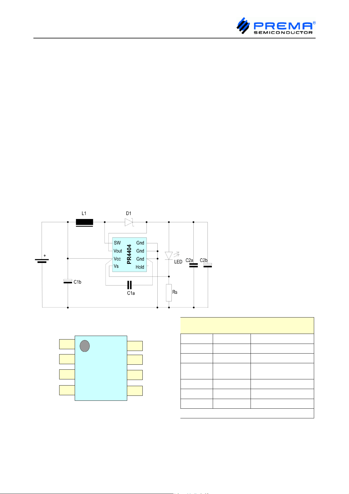
Typical Application Circuit
Pin Description PR4404
lot code
SW
Vout Gnd(sub
Vcc
Vs
1
2
3
4
date code
SZ22v10
8
Gnd(S)
7
Gnd(A)
6
Hold
5
Pin No Pin Name Pin Function
Description
1 SW driver output
2 Vout output voltage, rectified
3 Vcc battery supply input
4 Vs LED cathode / current
sense resistor
5 Hold shutdown
6 Gnd (A) ground (analog)*
7 Gnd (sub) ground (substrate)*
8 Gnd (S) ground (power)*
*Pins 6, 7, 8 must all be connected.
© PREMA Semiconductor GmbH 2008
Page 1/12 PRELIMINARY DATA Rev 3408
Page 2
LED DRIVER PR4404
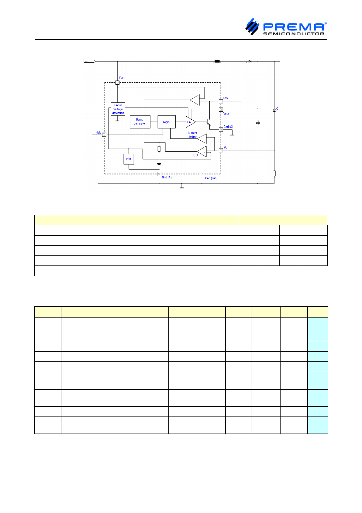
Block Diagram
Absolute Maximum Ratings
Parameter Min Typ Max Units
VCC (no damage) -0.3 8 V
SW output peak current 1.5 A
Operating junction temperature -20 125 °C
Storage Temperature Range -55 150 °C
Electrostatic Discharge (ESD) Protection 2 kV
Electrical Characteristics
Ta = 25°C, unless otherwise noted.
Symbol Parameter Conditions Min Typ Max Units
V
cc
V
sat
f
sw
V
FB
Supply Voltage, min. operating
min. startup
max. operating
0.89
1.00 1.05
5.0*
V
V
V
SW output transistor saturation 1.0A 0.4 V
Switching Frequency 300 700 kHz
Feedback voltage threshold at Vs 200 mV
Quiescent supply current Hold = LOW
Vcc > 850mV 2.0 3.0 mA
Icc Supply current Hold = open
Vcc > 850mV 2.0 3.0 mA
V
SW Clamp
Θ
JA
SW output clamping voltage 14
Thermal resistance
no air convection 160 K/W
junction - ambient
* but Vcc not higher than VF (LED)
© PREMA Semiconductor GmbH 2008
Page 2/12 PRELIMINARY DATA Rev 3408
Page 3
LED DRIVER PR4404
Typical Characteristics
This datasheet presents characteristics for different typical applications:
A. Supply voltage 1...2V - target current 100mA - one LED
B. Supply voltage 1...2V - target current 150mA - one LED
C. Supply voltage 1.5...3V - target current 300mA - one LED
D. Supply voltage 2...5V - target current 200mA - two LEDs in series
A and B are typical single battery-cell applications, C for two, and D for three cells.
The behaviour at many other operating conditions can be estimated by interpolation or
extrapolation.
Note that in the following diagrams the peak current through the output switch exceeds the
maximum rating.
Also the power dissipation can cause a junction temperature higher than the maximum
rating under some operating conditions.
These data should give an impression of the performance over the whole set of
parameters, but the fact that they are shown here should not be regarded as an approval
for operation under these conditions.
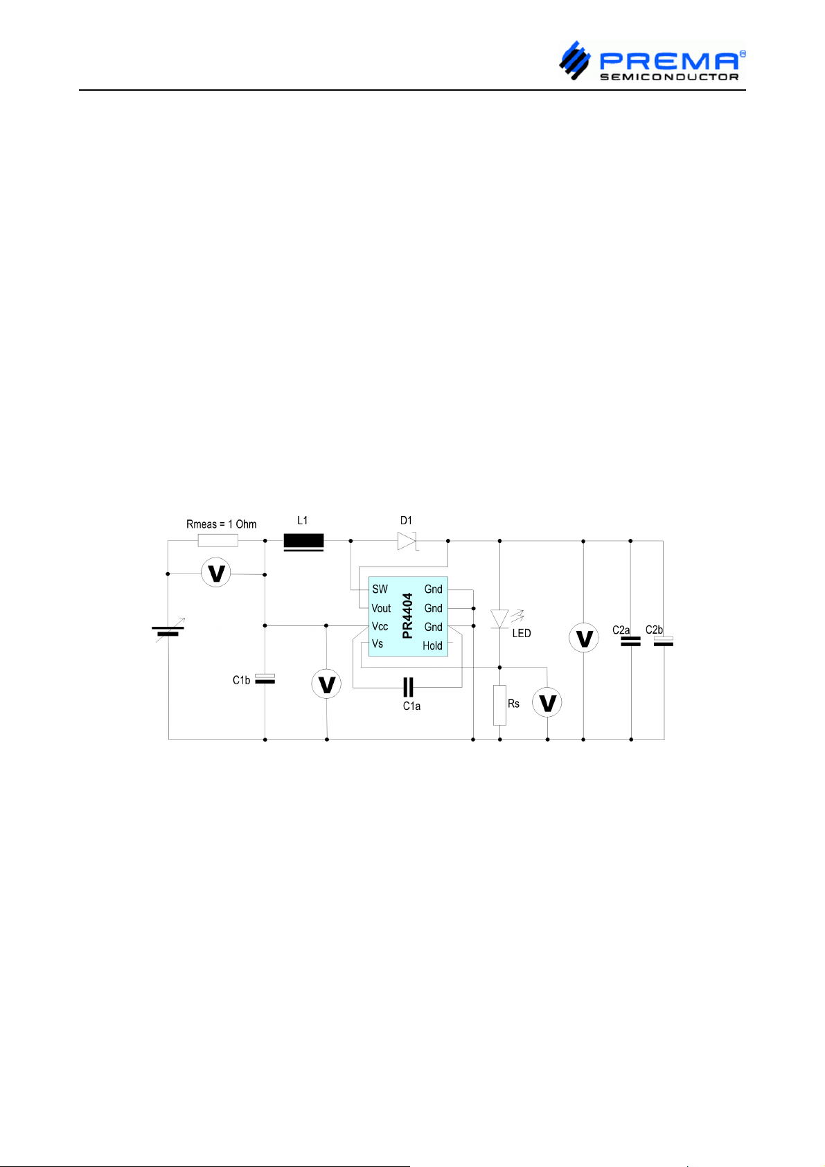
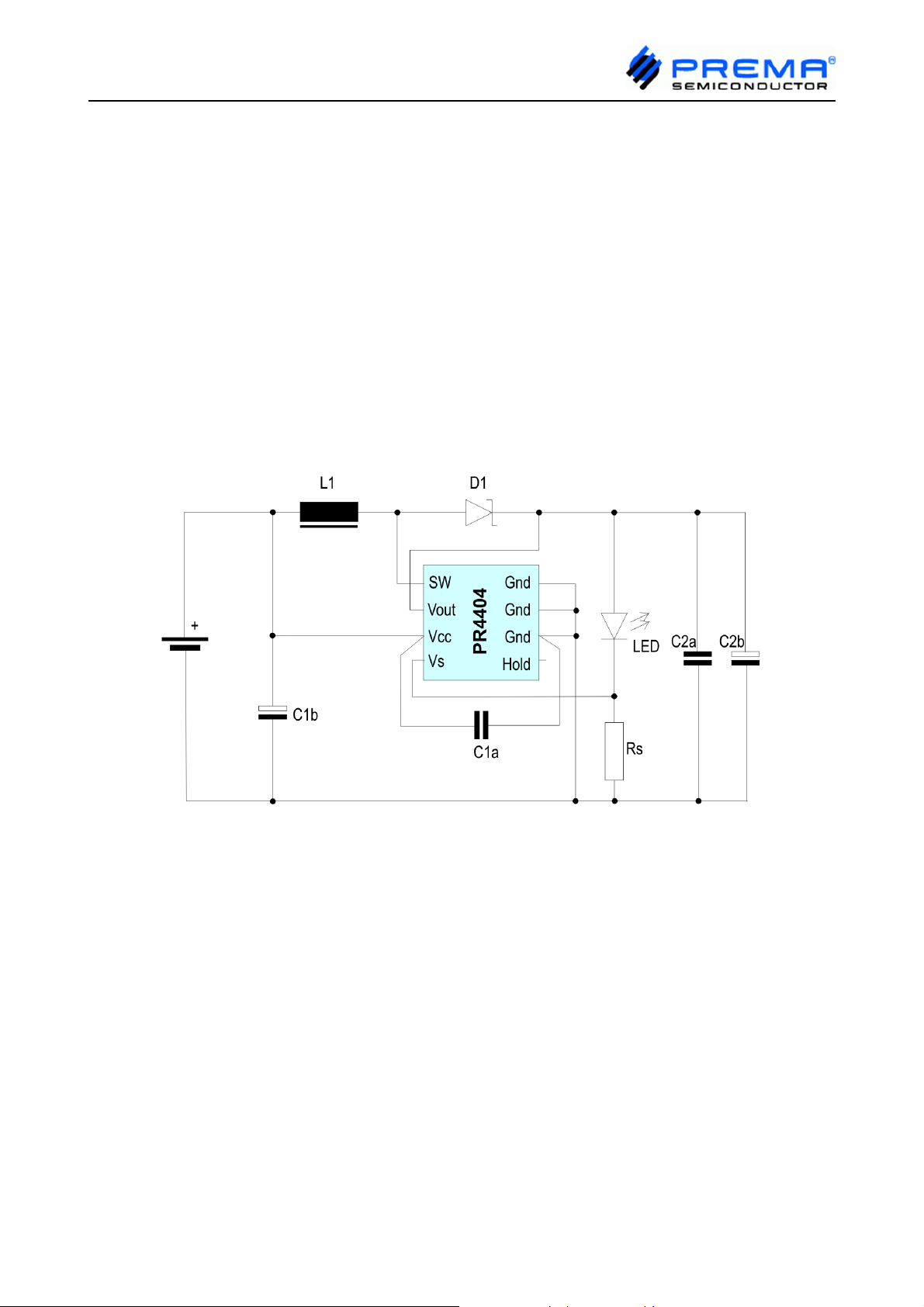
Test circuit
C1a: 1µF ceramic
C1b: 100µF tantalum
L1: Würth WE-PD XS series; inductance see diagrams
D1: MBRS140
Rs: see diagrams
C2a: 1µF ceramic
C2b: 100µF tantalum
© PREMA Semiconductor GmbH 2008
Page 3/12 PRELIMINARY DATA Rev 3408
Page 4
LED DRIVER PR4404
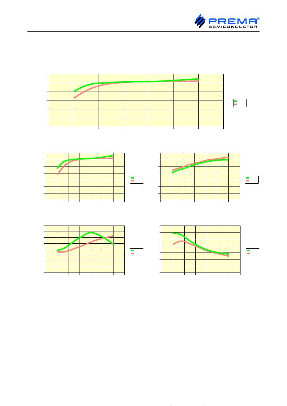
A. Supply voltage 1...3V - target current 100mA - one LED
Rs = 2 Ω , L1 = 1.0µH / 1.5µH with I
Output Current vs. Supply Voltage
120
100
80
60
40
20
Output current (mA)
0
0,8 1 1,2 1,4 1,6 1,8 2 2,2
Supply Voltage (V)
Output Power vs. Supply Voltage
350
300
250
200
150
100
Output pow er (mW)
50
0
0,8 1 1 ,2 1, 4 1,6 1 ,8 2 2,2
Supply Voltage (V )
=2.5A
sat
1.0 µ H
1.5 µ H
Efficiency vs. Supply Voltage
70
60
50
40
30
20
Efficiency (%)
10
0
0,8 1 1,2 1,4 1 ,6 1,8 2 2,2
Supply Voltage (V )
1.0 µ H
1.5 µ H
1.0 µ H
1.5 µ H
Frequency vs. Supply Voltage
800
700
600
500
400
300
200
Frequency (kHz)
100
0
0,8 1 1 ,2 1, 4 1,6 1 ,8 2 2,2
Supply Voltage (V )
0.6 µ H
1.0 µ H
700
600
500
400
300
200
100
0
Av erage input current (mA)
0,8 1 1,2 1,4 1,6 1,8 2 2 ,2
Average input current
Supply Voltage (V )
For best operation at supply voltages between 1.0 and 1.6V the 1.0µH inductance is the
best choice, while at higher voltages 1.5µH are recommended.
Generally, the peak input current is approximately twice the average input current.
1.0 µ H
1.5 µ H
© PREMA Semiconductor GmbH 2008
Page 4/12 PRELIMINARY DATA Rev 3408
Page 5
LED DRIVER PR4404
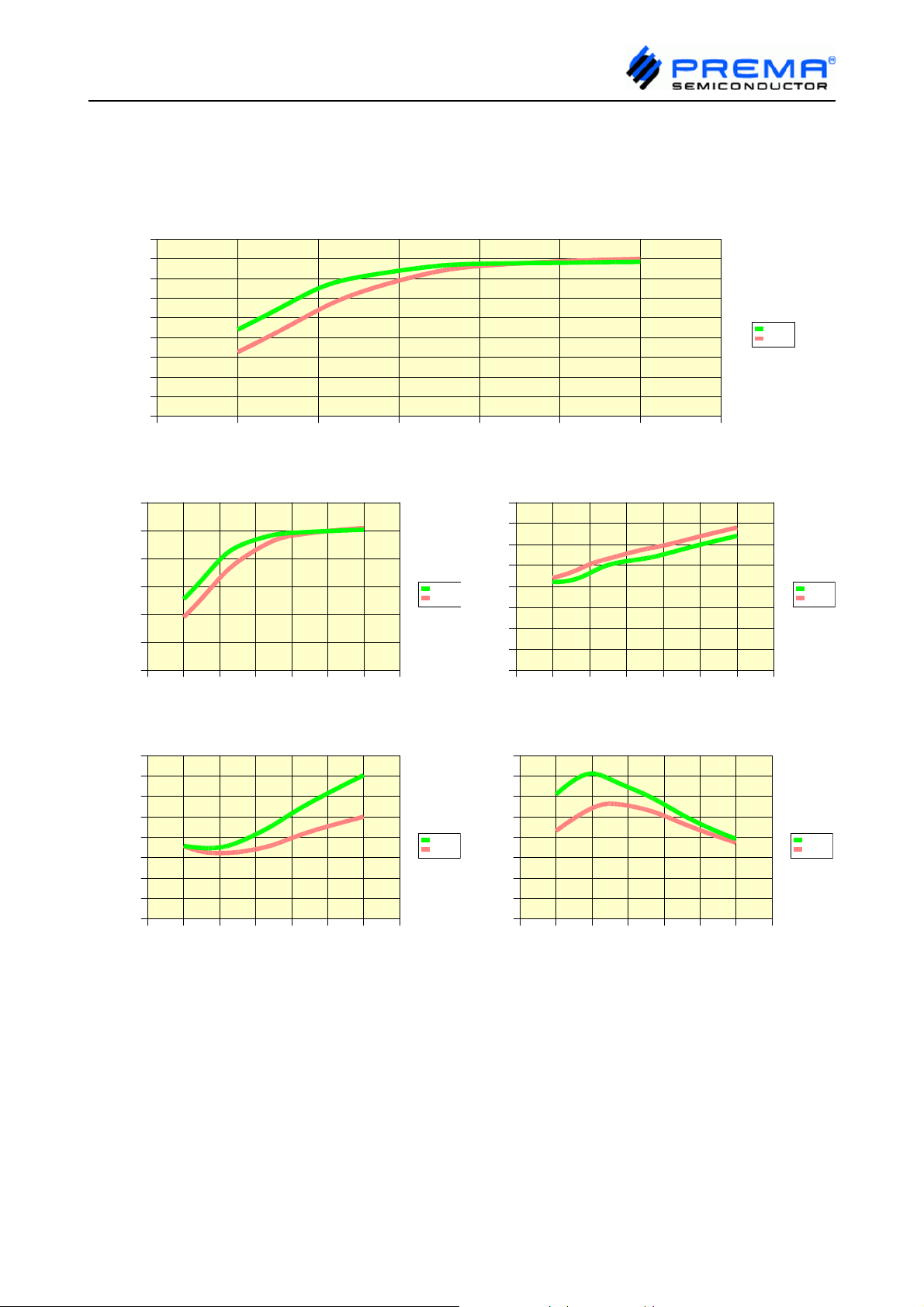
B. Supply voltage 1...2V - target current 150mA - one LED
Rs = 1.33 Ω , L1 = 1.0µH / 1.5µH with I
Output Current vs. Supply Voltage
180
160
140
120
100
80
60
40
Output current (mA)
20
0
0,8 1 1,2 1, 4 1,6 1,8 2 2, 2
Supply Voltage (V )
Output Power vs. Supply Voltage
600
500
400
300
200
Output pow er (mW)
100
0
0,8 1 1, 2 1,4 1,6 1,8 2 2 ,2
Supply Voltage (V )
=2.5A
sat
1.0 µ H
1.5 µ H
Efficiency vs. Supply Voltage
80
70
60
50
40
30
Efficiency (%)
20
10
0
0,8 1 1 ,2 1, 4 1,6 1 ,8 2 2,2
Supply Voltage (V )
1.0 µ H
1.5 µ H
1.0 µ H
1.5 µ H
Frequency vs. Supply Voltage
800
700
600
500
400
300
200
Frequency (kHz)
100
0
0,8 1 1,2 1,4 1,6 1 ,8 2 2,2
Supply Voltage (V )
1.0 µ H
1.5 µ H
800
700
600
500
400
300
200
Av erage input current (mA)
100
0
Average input current
0,8 1 1,2 1,4 1,6 1 ,8 2 2,2
Supply Voltage (V )
The peak input current is approximately twice the average input current.
At some conditions this current is close to the SW current maximum rating.
The allowed ambient temperature range is restricted by the maximum junction
temperature rating!
1.0 µ H
1.5 µ H
© PREMA Semiconductor GmbH 2008
Page 5/12 PRELIMINARY DATA Rev 3408
Page 6
LED DRIVER PR4404
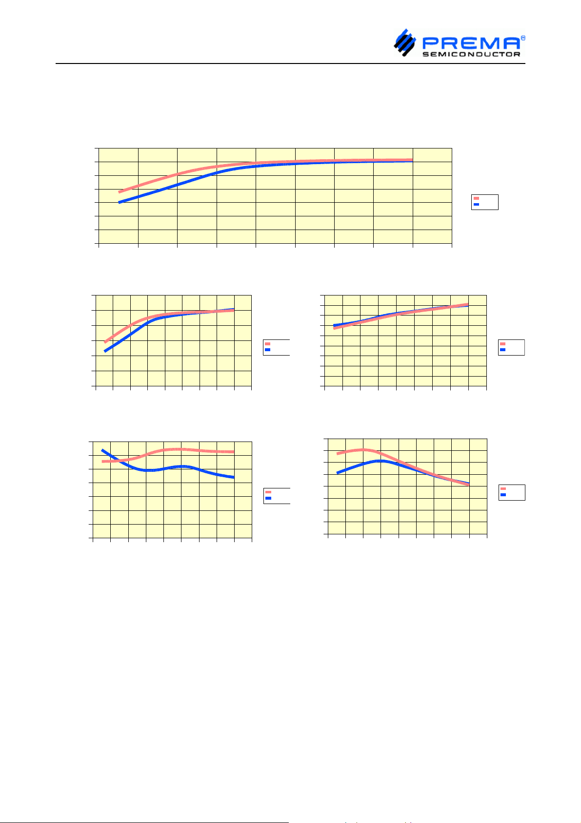
C. Supply voltage 1.5...3V - target current 300mA - one LED
Rs = 0.67 Ω , L1 = 1.5µH / 2.2µH with I
Output Current vs. Supply Voltage
350
300
250
200
150
100
Output current (mA)
50
0
1,4 1 ,6 1,8 2 2,2 2,4 2, 6 2,8 3 3,2
Supply Voltage (V )
Output Power vs. Supply Voltage
1200
1000
800
600
400
200
Output pow er (mW)
0
1,4 1,6 1,8 2 2,2 2,4 2,6 2,8 3 3,2
Supply Voltage (V )
=2.5A
sat
1.5 µ H
2.2 µ H
Efficiency vs. Supply Voltage
90
80
70
60
50
40
30
Efficiency (%)
20
10
0
1,4 1,6 1,8 2 2,2 2, 4 2, 6 2,8 3 3,2
Supply Voltage (V )
1.5 µ H
2.2 µ H
1.5 µ H
2.2 µ H
Frequency vs. Supply Voltage
350
300
250
200
150
100
Frequency (kHz)
50
0
1,4 1 ,6 1,8 2 2,2 2 ,4 2,6 2,8 3 3 ,2
Supply Voltage (V )
1.0 µ H
1.5 µ H
800
700
600
500
400
300
200
Av erage input current (mA)
100
0
Average input current
1,4 1 ,6 1,8 2 2,2 2 ,4 2,6 2,8 3 3 ,2
Supply Voltage (V )
The peak input current is approximately twice the average input current.
At some conditions this current is close to the SW current maximum rating.
The allowed ambient temperature range is restricted by the maximum junction
temperature rating!
1.0 µ H
1.5 µ H
© PREMA Semiconductor GmbH 2008
Page 6/12 PRELIMINARY DATA Rev 3408
Page 7
LED DRIVER PR4404
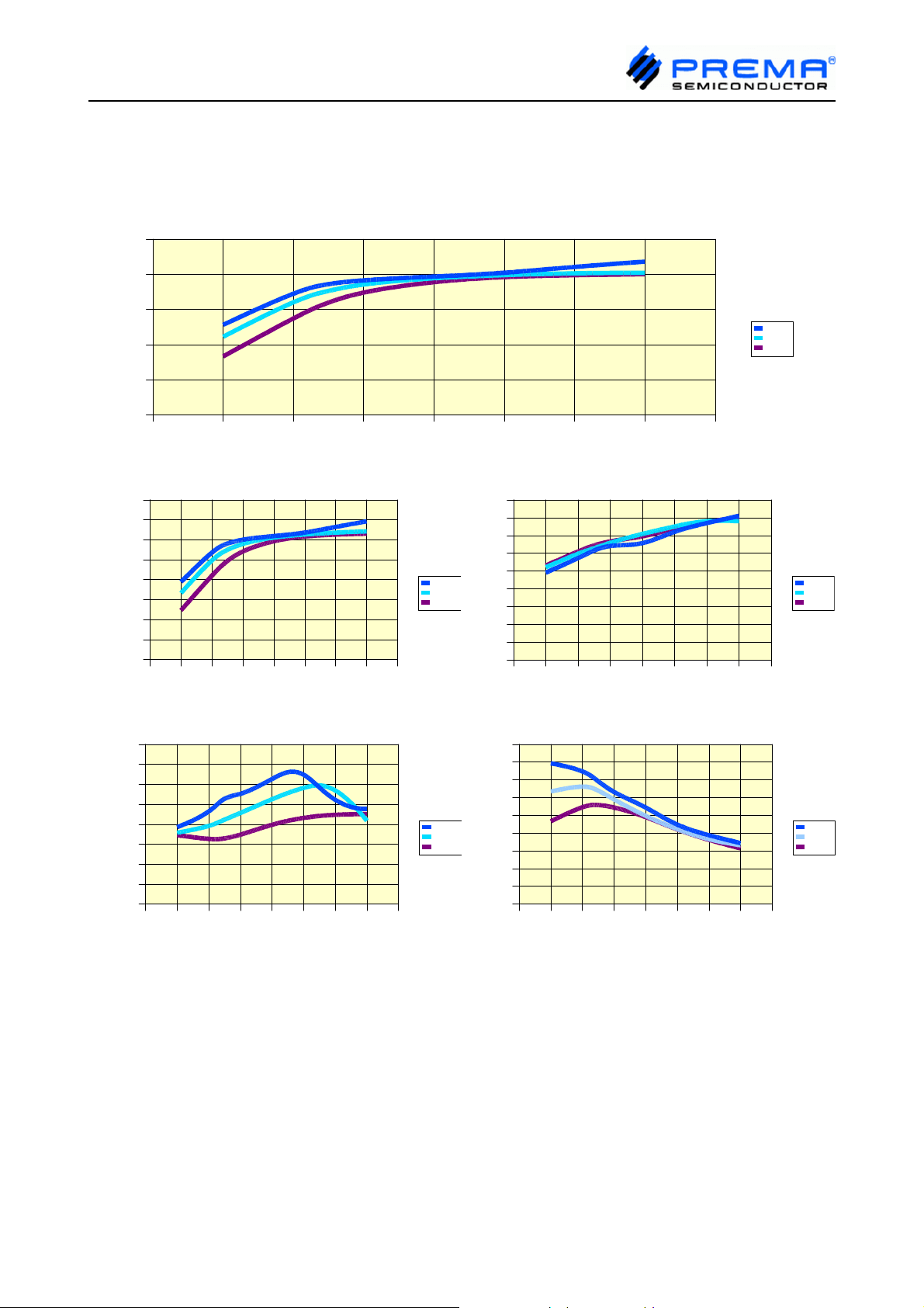
D. Supply voltage 2...5V - target current 200mA - two LEDs in series
Rs = 1 Ω , L1 = 1.5µH / 2.2µH / 3.3µH with I
Output Current vs. Supply Voltage (2 LEDs in series)
250
200
150
100
50
Output curr ent (mA)
0
1,5 2 2,5 3 3, 5 4 4,5 5 5, 5
Supply Voltage (V )
Output Power vs. Supply Voltage
1600
1400
1200
1000
800
600
400
Output Pow er (mW)
200
0
1,5 2 2,5 3 3,5 4 4,5 5 5 ,5
Supply Voltage (V )
1.5 µ H
2.2 µ H
3.3 µ H
=2.5A
sat
Efficiency vs. Supply Voltage
90
80
70
60
50
40
30
20
Efficiency (%)
10
0
1,5 2 2 ,5 3 3,5 4 4,5 5 5 ,5
Supply Voltage (V )
1.5 µ H
2.2 µ H
3.3 µ H
1.5 µ H
2.2 µ H
3.3 µ H
Frequency vs. Supply Voltage
800
700
600
500
400
300
Frequency (kHz)
200
100
0
1,5 2 2,5 3 3 ,5 4 4,5 5 5 ,5
Supply Voltage (V )
1.5 µ H
2.2 µ H
3.3 µ H
900
800
700
600
500
400
300
Mean input current (mA)
200
100
0
1,5 2 2,5 3 3 ,5 4 4,5 5 5 ,5
Mean input current
Supply Voltage (V )
1.5 µ H
2.2 µ H
3.3 µ H
As PR4404 is a boost converter, input voltages higher than the LED forward voltage
require two or three LEDs in series at the output.
With two LEDs in series, a stable output current of 200mA, or an output power of 1.2W,
can be achieved in the voltage range between 3.5V and 5V, which is interesting for three
battery cell applications.
Operation with a 2.2µH yields optimum results with best margins.
High input currents that occur at low input voltages can thermally overload the IC.
© PREMA Semiconductor GmbH 2008
Page 7/12 PRELIMINARY DATA Rev 3408
Page 8

LED DRIVER PR4404
Application Notes
General dimensioning guidelines
Current sense resistor Rs
Rs sets the peak output current, which is defined by I
Inductor L1
The best inductance depends mainly on the ratio between input and output voltage.
A high inductance results in a low frequency, limiting the transfered power at low supply
voltages.
A low inductance causes a shorter charging time, allowing a higher power transfer, but
resulting in a lower efficiency and eventually in an insufficient current regulation at higher
supply voltages.
So a proper balance between behaviour at the low end and high end of the supply voltage
range in the respective application should be found.
See diagrams and application examples for some recommendations.
The saturation current of the inductor must be at least equal to the peak current.
The peak current is approximately two times the average input current under worst-case
conditions, which mostly occur at low supply voltages.
Schottky diode D1
D1 must be capable driving the peak current, as for the inductor.
A low forward voltage at this current and a fast recovery provide a high efficiency.
Recommended diode types are MBRS140 or 1N5817.
LED
peak=VFB
/Rs.
Any type of LED can be used, as far as specified for the current.
However, the output voltage Vout must be higher than the input voltage Vcc; otherwise the
current regulation will not work properly. Therefore it is usually possible to drive one whitelight LED with VF=3.2V from two alkaline batteries with a nominal voltage of 3.0V, but not
from three NiMH cells with 3.6V.
The voltage at pin SW is internally clamped by a zener diode (for clamping voltage see
electrical specification). Therefore operation without output load does not damage the
chip. Nevertheless, prolonged operation without load should be avoided.
It is possible to connect two or more LEDs in series at the output. With increasing ratio of
Vout/Vcc the maximum output current decreases.
Mind that the built-in zener diode at SW limits the achievable output voltage and therefore
the number of LEDs that can be connected.
Capacitors C1, C2
C1 is a reservoir capacitor to stabilise the input voltage and prevent regulator oscillations.
It usually consists of a ceramic capacitor C1a in parallel to a tantalum capacitor C1b.
It is important to connect a ceramic capacitor of approx. 1µF between Vcc and Gnd very
close to the IC.
The size of the tantalum or electrolytic capacitor depends on the application. In some
cases it may be even dispensable, but mostly a capacitor of up to 100µF will improve the
© PREMA Semiconductor GmbH 2008
Page 8/12 PRELIMINARY DATA Rev 3408
Page 9
LED DRIVER PR4404
performance, as it smoothes out the peak current drain from the power source and allows
a battery to be used to a deeper discharge level.
Also C2 consists of a ceramic capacitor C2a and an electrolytic reservoir capacitor C2b at
the output, responsible for smoothing the pulsating output current through diode D1. Its
value depends on the current level and the allowed ripple height. Find some
recommended values in the application example circuits.
PCB
When designing the PCB layout, keep in mind that currents of up to 2A are involved. All
power lines, especially from the battery, inductor and SW input pin, must be sufficiently
wide to keep the voltage drop as low as possible.
The ceramic capacitor C1b must be placed close between Vcc and Gnd of the IC.
A large ground plane is helpful for good performance and low EMI.
Power Flashlight
Components:
for LED current 150mA:
Vcc: 1.2...1.5V (nominal)
C1a: 1µF
C1b: 100µF/6.3V
L1: 1.0µH, Isat ≥ 1.2A
D1: MBRS140 or 1N5817
Rs: 1.3 Ω
C2a: 470nF
C2b: 22µF/6.3V
© PREMA Semiconductor GmbH 2008
Page 9/12 PRELIMINARY DATA Rev 3408
for LED current 300mA:
Vcc: 2.4...3.0V (nominal)
C1a: 470nF
C1b: 100µF/6.3V
L1: 1.5µH, Isat ≥ 1.6A
D1: MBRS140 or 1N5817
Rs: 0.67 Ω
C2a: 470nF
C2b: 22µF/6.3V
Page 10
LED DRIVER PR4404
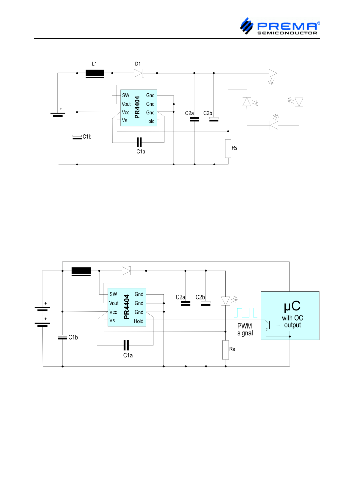
Driving a chain of LEDs
Output voltages up to 16V are possible. As the output power of the circuit is limited, the
maximum LED current is lower by a factor roughly equal to the number of LEDs compared
with single LED applications.
Recommended dimensions: see power flashlight, except Rs changed to VFB/I
LED
.
PWM controlled LED
The Hold input allows to switch on and off the LED with a digital circuit, such as a
microcontroller or a timer circuit.
This can be used e.g. for a PWM brightness control, for blinker circuits and many other
purposes.
Mind that no voltage must be applied at the Hold pin, but it must only be pulled down to
Gnd. Only an open collector or open drain output must be connected to Hold!
Due to the remaining quiescent current this feature is not recommended for soft-switching
battery-operated lamps on and off.
© PREMA Semiconductor GmbH 2008
Page 10/12 PRELIMINARY DATA Rev 3408
Page 11

LED DRIVER PR4404
Amax=TJmaxJA⋅Ptotal
Calculation of maximum ambient temperature
Under some operating conditions, especially at high voltage transfer ratios and with low
inductances, the IC can get into thermally critical states.
The following formula gives a rough estimtation of the maximum temperature at which the
circuit can be operated.
P
: output power (measured, or estimated from diagram)
out
η
: efficiency (measured, or estimated from diagram)
PIC: total power dissipation in IC
1
PIC≈
This formula assumes that the power loss occurs inside the IC and the current sense resistor, but neglects
the losses in the inductor, Schottky diode, wiring and capacitors.
T
: maximum ambient temperature
Amax
T
: maximum junction temperature (see Absolute Maximum Ratings)
Jmax
Θ
: thermal resistance of package (see Electrical Characteristics)
JA
T
: maximum ambient temperature
Amax
⋅P
outIout⋅Vsense
T
Example:
According to the diagrams, with a target current of 300mA, a 1.5µH inductor and one LED at the output, at
Vcc=2.2V the actual output power is 950mW, and the efficiency is 70%.
The power dissipated inside the IC can be estimated to
PIC ≈ 0.43 · 0.95W - 0.3A · 0.2V = 0.40W - 0.06W = 0.34W
Then the maximum ambient temperature is
T
= 125°C - 160K/W·0.34W = 70°C
Amax
For highest reliability a permanent operation near the thermal limits should be avoided.
Actual operating limits will depend on many factors. E.g. a PCB design with good heat spreading and forced
air convection may improve the situation, but a thermally sealed casing or heating from the LED or battery will
make it worse.
Also the efficiency in the actual application may differ from the values given in the diagrams.
With decreasing supply voltage the voltage transfer ratio and therefore the input current
rises, and the efficiency falls. As a consequence, the thermal load on the IC increases as
the supply voltage falls.
Therefore battery operated circuits must be designed that while discharging the battery no
critical state can occur.
© PREMA Semiconductor GmbH 2008
Page 11/12 PRELIMINARY DATA Rev 3408
Page 12
LED DRIVER PR4404
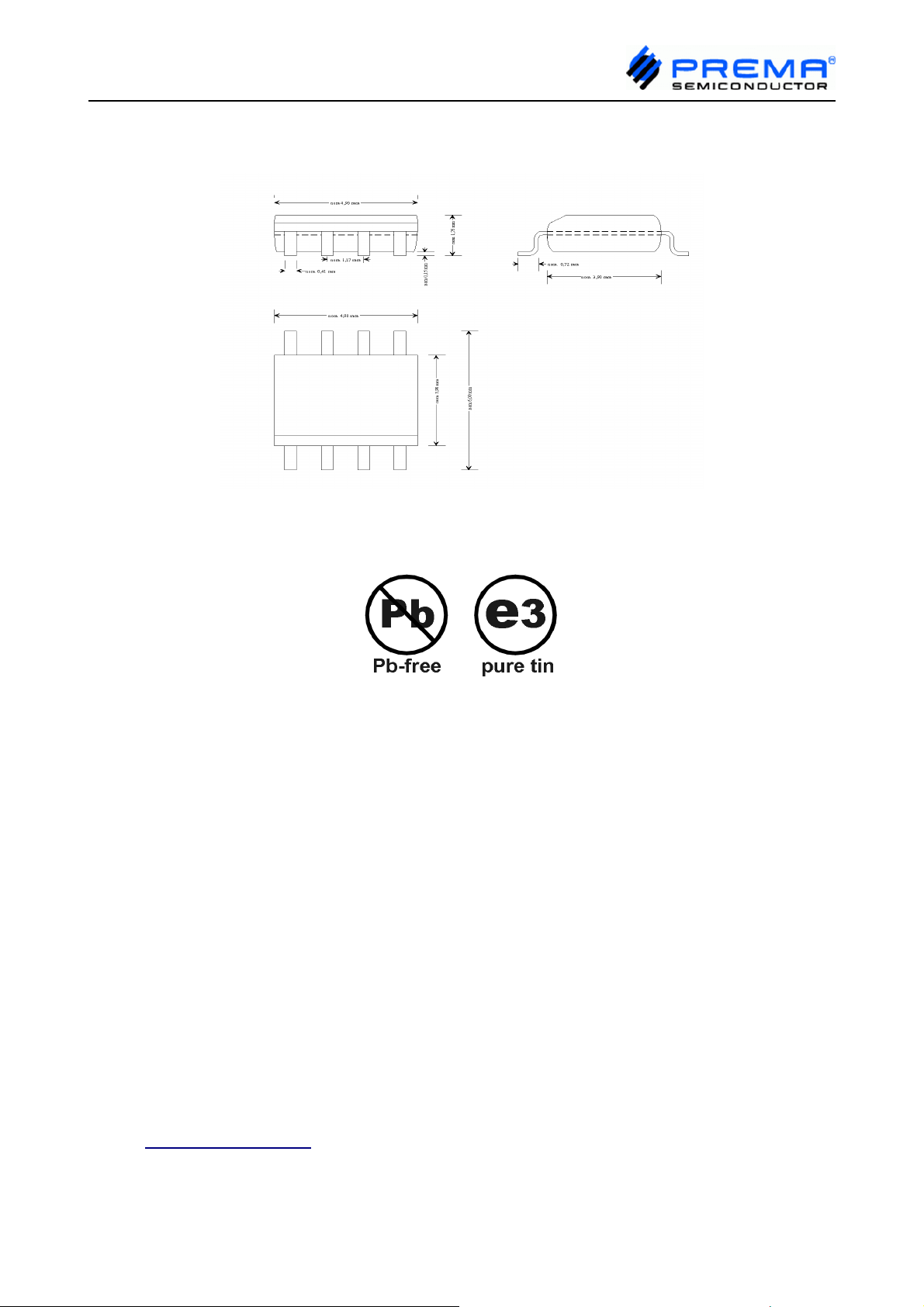
Available Package
Package type: 8L SOIC (150 mils)
All parts delivered comply with RoHS. Finish is pure tin.
Disclaimer
Information provided by PREMA is believed to be accurate and correct. However, no responsibility is assumed by PREMA for its use,
nor for any infringements of patents or other rights of third parties which may result from its use. PREMA reserves the right at any time
without notice to change circuitry and specifications.
Life Support Policy
PREMA Semiconductors products are not authorized for use as critical components in life support devices or systems without the
express written approval of PREMA Semiconductor. As used herein:
1. Life support devices or systems are devices or systems which, (a) are intended for surgical implant into the body, or (b) support or
sustain life, and whose failure to perform when properly used in accordance with instructions for use provided in the labeling, can be
reasonably expected to result in a significant injury to the user.
2. A critical component is any component of a life support device or system whose failure to perform can be reasonably expected to
cause the failure of the life support device or system, or to affect its safety or effectiveness.
PREMA Semiconductor GmbH
Robert-Bosch-Str. 6
55129 Mainz Germany
Phone: +49-6131-5062-0
Fax: +49-6131-5062-220
Email: [email protected] Web site: www.prema.com
© PREMA Semiconductor GmbH 2008
Page 12/12 PRELIMINARY DATA Rev 3408
 Loading...