

0
0
0
e
0
0
0
0
0
0
0
0
0
0
0
0
0
0
0
0
0
0
0
0
0
0
0
e
0
0
0
0
0
0
0
e
0
0
e
0
e
0
e
e
pREAMBLE
- VIINSTRUMENTS
1850A and 1855A
DIFFERENTIAL AMPLIFIERS
March 10, 1999
PREAMBLE INSTRUMENTS, Inc,
P.O. Box 6118
Beaverton, OR 97007-0118
0
0
0
0
0
0
0
0
0
0
0
0
0
0
0
0
0
0
0
0
0
0
0
0
0
0
0
0
0
0
0
0
0
0
0
0
0
0
0
0
0
0
0
O
03-10-99
TABLE OF CONTENTS
Section 1 SPECIFICATIONS
Introduction ............................................................................. 1 - l
1850/1855A Specifications ......................................................
1-2
Power Requirements & Physical Characteristics ..................... 1-3
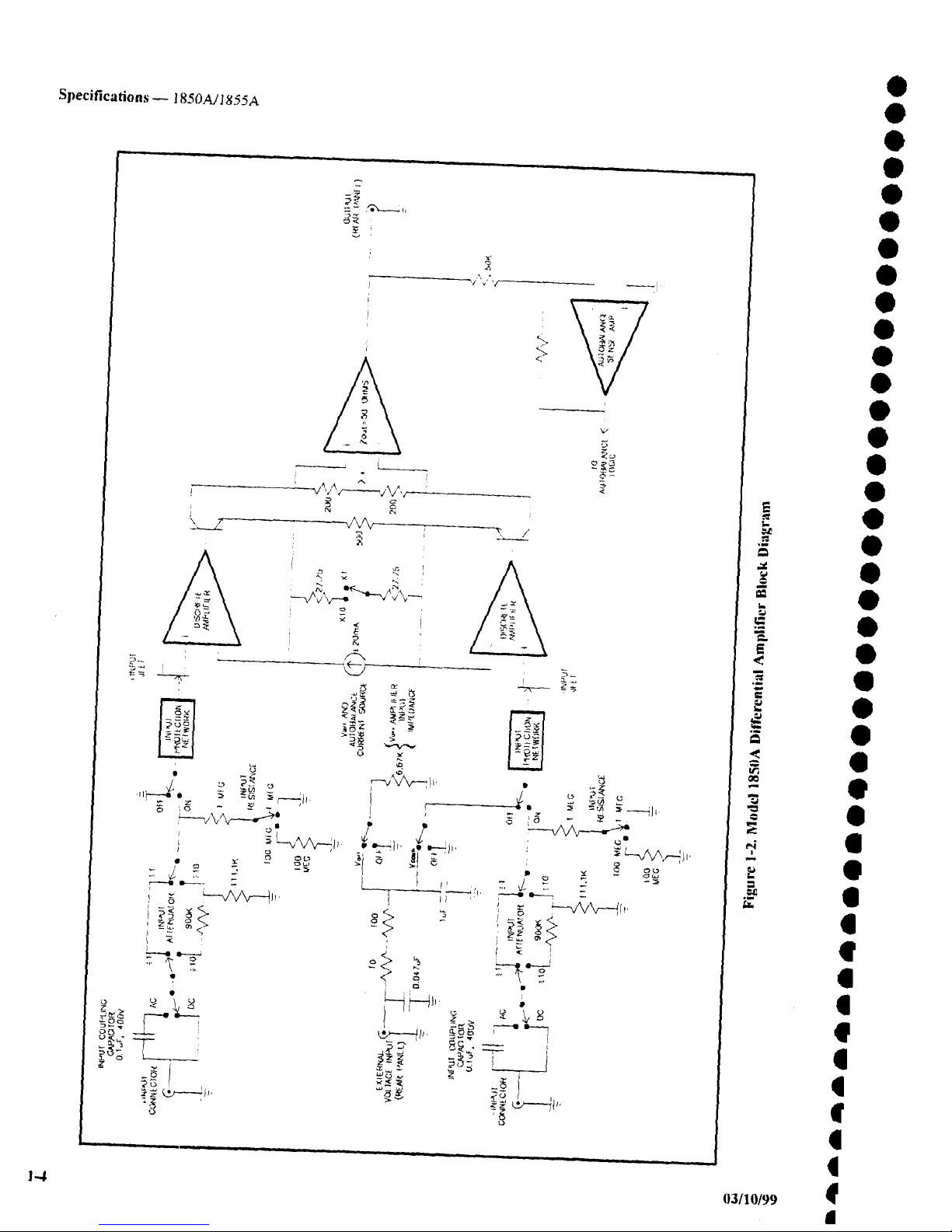
1850 Block Diagram ................................................................ 1-4
1855A Block Diagram ............................................................. 1-5
Section 2
OPERATING INSTRUCTIONS,
CONTROLS AND INDICATORS
Front Panel ............................................................................... 2-1
Rear Panel ................................................................................ 2-4
New Features of 1850A and 1855A ......................................... 2-5
Oscilloscope Settings ............................................................... 2-6
Model 1850 Operation ............................................................. 2-7
Section 3 GENERAL OPERATING INFORMATION
Getting Started ......................................................................... 3-1
Power Connection ....................................................................
3-1
1855A Front Panel Operation .................................................. 3- I
Attenuator and Gain Operation ................................................ 3-1
Comparison Voltage Operation ............................................... 3-2
Differential Offset Operation ...................................................
3-3
Which Offset Mode Should Be Used? .....................................
3-4
Operator Traps to Avoid .......................................................... 3-4
1850A/1855A
1850A/1855A
INITIAL SCOPE AND 1855 SETUP
L_ .............
7----
’
........
~---
i ’
SELECT 50 OHM INPUT
OR
PROVIDE 60 OHM TERMINATOR
~,.~
50mV/I)fV
I
v ~.ImV/DIV
Posmo
"~’ SET SENSITMTY TO 50mVldiv
DURING OPgRA13ON. USE
ON LY 5OmvIoN ON
MORE SENSITIVE PosmoN$
POSITION TRACE TO CENTER <
SCREEN (DC OFFSET = OFF)
00 NOT USE TH E SCOPE
POSmON OR OFFSE’f
AFrER THIS INIT~L SETUP
~ AC
/
~, ’f oc
’~ o:
//,!
///’
@ SELECT DCINPUTCOUPLING
//
s
’ /
/
//
,/
CONNECT AMPLIFIER OUTPUT TO
SCOPE INPUT WITH 50 OHM COAX
~
.........
mE
LJ ~e~ ~ ~ ~
’ ’~’
--"~< "
/,
l g ] ATTACH XCl00 PROBES ~ ~’2"
DO NOT ADJUST PROBE COMPENSATION
~THOUT FIRST REFERRING TO THE MANUAL
TRACE ON ~COPE
USE VDIFF AND PVG TO POSITION
~i PVG DI|PLAYS THS VOLTAGE OF THE SIGNAL AS ff
PASSES THROUGH THE SCOPE DIEPLAY CENTERLIRE.
(RE~IRRED TO THE PROIE I~P)
CONNECT PROBE CODING LEAD TO
PROBE CODE INPUT ON 1866 REAR PANEL
ii
03116/99
e
o
o
i
i
e
e
e
e
o
o
e
e
e
e
e
o
o
e
o
e
o
e
o
o
o
i)
o
o
e
e
o
o
o
o
o
e
e
o
o
o
o
o
o
0
0
0
0
0
0
0
0
0
0
0
Specifications- 1850A/1855A
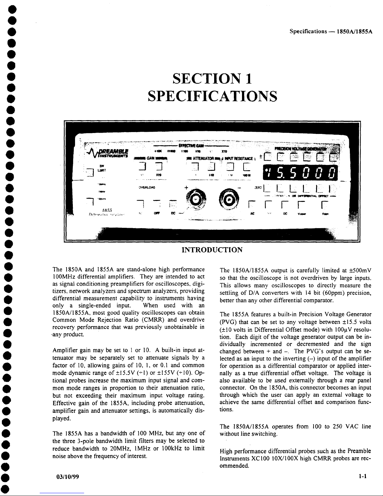
SECTION 1
SPECIFICATIONS
0
0
0
0
0
0
0
0
0
0
0
0
0
0
0
0
0
0
0
0
0
0
0
0
0
INTRODUCTION
The 1850A and 1855A are stand-alone high performance
100MHz differential amplifiers. They are intended to act
as signal conditioning preamplifiers for oscilloscopes, digitizers, network analyzers and spectrum analyzers, providing
differential measurement capability to instruments having
only a single-ended input. When used with an
1850A/1855A, most good quality oscilloscopes can obtain
Common Mode Rejection Ratio (CMRR) and overdrive
recovery performance that was previously unobtainable in
¯ any product.
Amplifier gain may be set to 1 or 10. A built-in input attenuator may be separately set to attenuate signals by a
factor of 10, allowing gains of 10, I, or 0.1 and common
mode dynamic range of_15.5V (+1) or +_.155V (+10).
tional probes increase the maximum input signal and common mode ranges in proportion to their attenuation ratio,
but not exceeding their maximum input voltage rating.
Effective gain of the 1855A, including probe attenuation,
amplifier gain and attenuator settings, is automatically displayed.
The 1855A has a bandwidth of 100 MHz, but any one of
the three 3-pole bandwidth limit filters may be selected to
reduce bandwidth to 20MHz, IMHz or 100kHz to limit
noise above the frequency of interest.
03/i 0/99
The 1850A/1855A output is carefully limited at +500mV
so that the oscilloscope is not overdriven by large inputs.
This allows many oscilloscopes to directly measure the
settling of D/A converters with 14 bit (60ppm) precision,
better than any other differential comparator.
The 1855A features a built-in Precision Voltage Generator
(PVG) that can be set to any voltage between +15.5 volts
(+10 volts in Differential Offset mode) with 100~tV resolution. Each digit of the voltage generator output can be individually incremented or decremented and the sign
changed between + and -. The PVG’s output can be selected as an input to the inverting (-) input of the amplifier
for operation as a differential comparator or applied inter-
nally as a true differential offset voltage. The voltage is
also available to be used externally through a rear panel
connector. On the 1850A, this connector becomes an input
through which the user can apply an external voltage to
achieve the same differential offset and comparison func-
tions.
The 1850A/1855A operates from 100 to 250 VAC line
without line switching.
High performance differential probes such as the Preamble
Instruments XC100 10X/100X high CMRR probes are rec-
ommended.
i-1
Specifications m 1850A/1855A
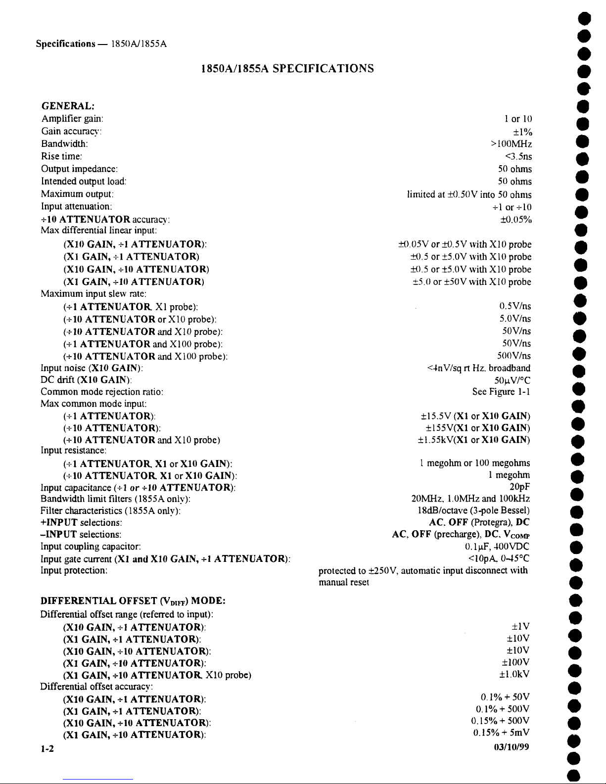
1850A/1855A SPECIFICATIONS
GENERAL:
Amplifier gain:
Gain accuracy:
Bandwidth:
Rise time:
Output impedance:
Intended output load:
Maximum output:
Input attenuation:
+10 ATTENUATOR accumc3.,:
Max differential linear input:
(X10 GAIN, +1 ATTENUATOR):
(X1 GAIN, +1 ATTENUATOR)
(X10 GAIN, +I0 ATTENUATOR)
(X1 GAIN, +10 ATTENUATOR)
Maximum input slew rate:
(+1 ATTENUATOR. X1 probe):
(+Ill ATTENUATOR or X10 probe):
(+10 ATTENUATOR and X10 probe):
(+1 ATTENUATOR and XI00 probe):
(+Ill ATTENUATOR and X100 probe):
Input noise (X10 GAIN):
DC drift (X10 GAIN):
Common mode rejection ratio:
Max common mode input:
(+1 ATTENUATOR):
(+Ill ATTENUATOR):
(+10 ATTENUATOR and X10 probe)
Input resistance:
(+1 ATTENUATOR. X1 or X10 GAIN):
(+10 ATTENUATOR. X1 or X10 GAIN):
Input capacitance (+1 or +10 ATTENUATOR):
Bandwidth limit filters (1855A only):
Filter characteristics ~ 1855A only):
+INPUT selections:
-INPUT selections:
Input coupling capacitor:
Input gate current (X1 and X10 GAIN, +1 ATTENUATOR):
Input protection:
DIFFERENTIAL OFFSET (VDIFF) MODE:
Differential offset range (referred to input):
(X10 GAIN, +I ATrENUATOR):
(X1 GAIN, +1 ATTENUATOR):
(XI0 GAIN, +10 ATTENUATOR):
(X1 GAIN, +10 ATTENUATOR):
(XI GAIN, +10 ATTENUATOR. X10 probe)
Differential offset accuracy:
(X10 GAIN, +I ATTENUATOR):
(X1 GAIN, +1 ATTENUATOR):
(X10 GAIN, +10 ATTENUATOR):
(XI GAIN, +10 ATTENUATOR):
1-2
1 orl0
+_1%
>I00MHz
<3.5ns
50 ohms
50 ohms
limited at +0.50V into 50 ohms
+1 or +10
_+0.05%
N).O5V or +0.5V with XIO probe
N).5 or +5.0V with XIO probe
_+0.5 or +-5.0V with XIO probe
_+5.0 or +50V with XIO probe
O. 5 V/ns
5.0V/ns
50V/ns
50V/ns
500V/ns
<4nV/sq rt Hz. broadband
50~V/°C
See Figure 1-1
+15.5V (X1 or X10 GAIN)
+-I55V(X1 or X10 GAIN)
+l.55kV(Xl or X10 GAIN)
1 megohm or 100 megohms
1 megohm
20pF
20MHz. 1.0MHz and 100kHz
18dB/octave (3-pole Bessel)
AC, OFF (Pmtegra),
AC, OFF (precharge), DC, Vco~
0.1 ~tF, 400VDC
<10pA. 0-45°C
protected to +_250V, automatic input disconnect with
manual reset
+-lV
+IOV
+-IOV
+lOOV
+l.OkV
0.1% + 50V
0.1% + 500V
0.15% + 500V
0.15% + 5mV
03/10/99

0
0
0
0
0
0
0
0
0
0
0
0
0
0
0
0
0
0
0
0
0
0
0
0
0
0
0
0
0
0
0
0
0
0
0
0
0
0
0
0
0
0
0
0
COMPARISON OFFSET (Vco~tp) MODE:
Effective comparison voltage range:
(+1 ATTENUATOR):
(+10 ATTENUATOR):
(Xl0 probe and +10 ATTENUATOR):
PRECISION VOLTAGE SOURCE (1855A only):
Output range:
DC accuracy:
Resolution:
Control:
Temperature coefficient:
Type:
Output:
PVG AUTO ZERO:
POWER REQUIREMENTS
Line voltage requirement:
Line frequency range:
Power requirement:
ENVIRONMENTAL CHARACTERISTICS
Operating Range:
Non-Operating:
PHYSICAL CHARACTERISTICS
Height:
Width:
Depth:
Weight:
Shipping Weight:
Specifications- 1850A/1855A
’_15.5V (Xl or Xl0 GAIN)
+155V (Xl or Xl0 GAIN)
1.55kV (Xl or Xl0 GAIN)
+15.5V
0.05% of reading +500~V (0° to 50°C)
100~tV
All digits are addressable. Digit carries to next decade
typically <5ppm/°C of full scale
Oven stabilized buried Zener
Applied to inverting input and available at rear panel
Sets output to zero when 0.0 volts selected and
in error by more than 0.5mV thereafter
100 to 250VAC
48 - 66Hz
35 W maximum
0 to 50°C
-40 to 75°C
7,29cm (2.87")
21.2cm (8.36")
23.2cm (9.12")
2.15kg (4.751b)
3.12kg (6.881b)
c
M
R
R
1000000
100000
~-- i
I
i.
1000~
1000
i
100 :
i ,
’ i
i
|0 I
I
AMPLIF’IER SE’I’T1NGS
t
XI OR Xl0 GAIN. XI Aq~’ENUATOR L
1 RHz
10 kHz 100 kHz
1 MHz 10 MHz
100 MHz
Figure 1-1. CMRR vs Frequency
1131111199
1-3
1-4
Specifications ~ 1850A/1855A
03110199
O
O
O
O
O
O
O
O
O
O
O
O
0
O
O
O
O
O
O
0
O
O
|
O
O
O
O
e
O
II
O

0
0
0
0
0
0
0
0
0
0
0
0
0
0
0
0
0
0
0
0
0
0
0
0
0
0
0
0
0
0
0
0
0
0
0
@
0
0
03/10/99
Specifications- 1850A/1855A
\

0
0
0
9
0
0
0
0
0
0
0
0
0
0
0
0
0
0
0
0
0
0
0
0
0
0
0
0
0
0
0
0
0
0
0
0
0
0
0
0
0
0
0
0
Operating Instructions, Controls and Indicators-- 1850A/1855A
SECTION 2
OPERATING INSTRUCTIONS, CONTROLS
AND INDICATORS
FRONTPANEL
ATTENUATOR
Signals connected to the +INPUT and the -INPUT are
connected either directly to the 1850A/1855A’s amplifier
inputs or to the input attenuators. The input attenuators are
passive networks which divide each signal by ten.
In +1 mode the front panel input connectors are directly
connected to the 1850A/1855A amplifier’s differential in-
puts.
In +10 mode each front panel input connector is connected
to a passive 1 megohm attenuator. The attenuator output is
connected to the 1850A/1855A amplifier’s corresponding
differential input. The signal at each input is attenuated bv
a factor of ten.
GAIN
The 1850A/1855A amplifier gain (amplification) is select-
able between XI and Xl0. The amplified signal appears at
the rear panel AMPLIFIER OUTPUT connector.
A signal connected to the +INPUT will maintain its polarity at the output connector. A signal connected to the
-INPUT will be inverted in polarity.
Proper gain is obtained when the 1850A/1855A drives a 50
ohm load such as an oscilloscope with input impedance set
to 50 ohms. An oscilloscope with only a 1 megohm input
impedance available should have a 50 ohm coaxial termi-
nation placed on its input connector. The 1850A/1855A is
then connected to the oscilloscope through the coa.,dal ter-
mination.
The amplifier gain and the input attenuator are individually
selectable to provide versatility. For example, the compari-
son voltage range is changed from +15.5000 to +155.000
volts by changing the ATTENUATOR from +1 to +10.
The overall gain can still be set to either 1 or 0.1 by selecting the GAIN mode, Xl0 or Xl, as desired.
AUTO ZERO is a feature invoked when either the Xl or
Xl0 button is pushed, even if a different gain is not se-
lected. AUTO ZERO momentarily sets the input coupling
to OFF and determines the offset necessary, to set the out-
put at 0 volts within about 25~V. During this process the
front panel is unresponsive. When finished, the input coupling returns to its previous mode. AUTO ZERO usually
takes less than one second. This handv feature allows the
operator to DC balance the 1850A/1855A simply by push-
ing the GAIN button which is already illuminated. When
changing gains, the AUTO ZERO feature is automatically
invoked, freshly adjusting the amplifier’s DC balance.
+INPUT COUPLING (AC OFF DC)
,oo .cZ% ~, ,_2~
In OFF mode, the input connector is disconnected from the
amplifier input_ and the amplifier input is connected to
ground. The AC coupling capacitor is connected between
the +INPUT and ground through 1 megohm (either the
input attenuator or the input resistor), independent of the
INPUT RESISTANCE selected. In this mode, the AC
coupling capacitor is quickly charged to the average DC
input voltage. OFF mode is also referred to as precharge
mode. Precharge is particularly useful when planning to
AC couple and measure voltages in excess of 19 volts. The
1850A/1855A input coupling is set to OFF and connected
to the circuit under test. When the +INPUT is changed
from OFF to AC mode, the coupling capacitor is already
charged, and the trace properly centered on the oscilloscope
screen. Additionally, the risk of tripping the input overload
detector and automatically disconnecting the input is eliminated.
In the AC mode, the +INPUT is connected through an AC
coupling capacitor to the amplifier input or the input at-
tenuator. The coupling capacitor retains its charge when the
input is switched to I)C, making it possible to return to the
same circuit without the precharge time. But this also
makes it possible to discharge the coupling capacitor into
another circuit under test if its DC voltage differs by more
than approximately 19 volts from the voltage on the cou-
pling capacitor. The discharge current is limited to about
70mA, but this could damage some circuits. It is therefore
03/10/99
2-1

Operating Instructions, Controls and Indicators-- 1850A/1855A
recommended that the +INPUT coupling first be changed
to OFF (precharge) when measuring a new circuit point.
This will safely recharge the AC coupling capacitor in less
than 0.3 seconds. The AC coupling capacitor is 0. I~F and
rated at 400VDC.
DC and low frequencies are attenuated by the AC coupling
capacitor and the input resistance. With the ATTEN-
UATOR set to +Ill, or set to +1 with the INPUT
RESISTANCE set to 1 megohm, the low frequency cut off
(-3dB point) is approximately 1.6Hz, lower than most oscilloscopes by a factor of 5. When the input attenuator is set
to +1, the INPUT RESISTANCE may be set to I00 megohms, and the -3dB point is 0.016Hz. This extremely low
frequency cut off is often handy in observing low frequency noise riding on large (up to 400 volts) DC voltages.
In the DC mode. the +INPUT connector is connected to
the amplifier either directly or through the input attenuator,
and the AC and DC attenuation are the same.
-INPUT COUPLING (AC OFF DC Vco~n,)
inverting input. The 1850A/1855A output is therefore zero
whenever these two voltages are equal. For this reason, the
voltage applied to the inverting input is called a comparison
voltage, Vco.~n,.
Vco.~p is often used to make precise measurements of large
signals by comparing the accurately known Vco,~n, with the
unknown signal. It can also be used to measure the actual
voltage at any point of a waveform
PRECISION VOLTAGE GENERATOR (PVG) output
range is +15.500 volts. The PVG is never attenuated bv the
input attenuator. Attenuation of the +INPUT signal bv the
+11) input attenuator will cause the PVG to null out an input
voltage up to +155.01) volts which is ten times larger than
the actual PVG voltage. When the 1855A is used with at-
tenuating probes that feature readout, the PVG display is
changed to indicate the voltage at the +INPUT probe tip
which will bring the amplifier output to zero.
The -INPUT connector is not useable when Vco~n, is selected.
r~uu ’~ ve~o
pqrc,S,t3N
x --
err
:.’,~AC,VO~
-.’~ 7-=- .....
t-T-7
"
<~> ~ utc,
r;"
,c
¯
~(S,SlANCC
The -INPUT has the same coupling modes as the +INPUT
plus one additional option, Vco~, (comparison voltage).
The 1855A generates a voltage controlled by the push buttons above and below the front panel numerical display.
This voltage is called the Precision Voltage Generator
(PVG). The 1850A does not have a built-in PVG and the
user must supply a dc voltage in the range of -15.5V to
+ 15.5V to the rear panel OFFSET connector.
In Vco~n, mode, the 1855A’s PVG is connected to the amplifier’s inverting input through an internal filter designed
to eliminate radio and television signal interference. The
1850A does not have the PVG, but uses an externally sup-
plied voltage. See Page 2-6 for Vco~ operation with the
1850A.
The 1850A/1855A’s amplifier subtracts the voltage applied
to its inverting input from the voltage applied to its non-
VDxw (differential offset voltage) is an instrument mode
rather than a type of input coupling. The Vmrr mode ’allows
the PVG (or an external source in the case of the 1850A)
inject an offset signal into the 1850A/1855A while still
using both inputs for full differential operation. This mode
can be used as a position control to move the trace on the
oscilloscope screen in preference to using the oscilloscope’s
position or offset control. The oscilloscope’s position and
offset controls should alwavs be set to zero so that the
1850A/1855A’s dvnamic range is properly centered. Op-
eration of the 1850A/1855A using the VDXW function is the
same as VcoMr except for the following:
¯ The -INPUT remains active, allowing full use of the
1850A/1855 A as a differential amplifier.
¯ The maximum range of the PVG (1855A) or the external
source (1850A) is _+10.000 volts in X1 GAIN and ±1.0000
volts in X10 GAIN. The effects of the +10 input
ATTENUATOR and probe attenuation are the same as
when using Vcosn,, i.e., any input attenuation multiplies the
effective offset.
¯ The VDtrV mode offset accuracy is slightly less than that
obtained using Vcosw.
The 1855A’s PVG display is changed to indicate the voltage that. if applied between the +INPUT and -INPUT,
would bring the amplifier output to zero. When the 1855A
is used with attenuating probes which feature readout, the
PVG display is scaled to include the effect of probe attenuation.
2-2
03110199
O
O
O
O
O
O
O
O
O
O
O
O
O
O
O
O
O
O
O
O
O
O
O
O
O
O
O
O
O
O
O
O
O
O
O
O
O
O
O
O
0
0
O

0
0
0
0
0
0
0
0
0
0
0
0
0
0
0
0
0
0
0
0
0
0
0
0
0
0
0
0
0
0
0
0
0
0
0
0
0
0
0
0
0
0
0
0
Operating Instructions, Controls and Indicators- 1850A/1855A
INPUT RESISTANCE
When the input ATTENUATOR is set to +1. the input
resistance can be increased from 1 megohm to 100 megohms. This is advantageous when measuring high impedance circuits or when AC coupling is needed with a very.
low frequency cut off.
Unbalanced source impedances can have an adverse effect
on common mode rejection. For example, a differential
source with impedances of 1000 and 2000 ohms, each
loaded with 1 megohm will have a common mode rejection
ratio (CMRR) of 1000 to I. The common mode rejection
ratio can be improved to 100,000 to 1 by using 100 megohm input resistance.
This limitation is also apparent when trying to make accurate measurements using VcoMP. A 10.000 volt reference
with a I000 ohm output impedance will be reduced to
9.9900 volts by the 1850A/1855A 1 megohm input resistance, introducing a 10mV error in the measurement. Increasing the input resistance to 100 megohms decreases this
error to 1001aV.
Oscilloscope inputs have a small input current which can
cause an offset when measuring high impedance circuits.
The offset can be observed by opening and shorting the
input to ground. The 1850A/1855A has a temperaturecompensated input current pull away (cancellation) which
works in both the 1 megohm and 100 megohm INPUT
RESISTANCE modes. Its input offset current is considerably less than that of most oscilloscopes.
EFFECTIVE GAIN (1855A ONLY)
Six lights (LEDs) across the top of the 1855A front panel
indicate the total gain from the instrument input to output.
When the XI light is lighted, the overall amplifier voltage
gain (amplification) is unity. Similarly, XI0 indicates
overall amplification of ten times. +10 indicates the voltage
amplification is 0. I, and so forth.
When Preamble Instruments or other encoded probes are
properly used. the effective gain includes the probe’s at-
tenuation factor.
BW LIMIT (1855A ONLY)
FULL -- The 1855A amplifier’s full bandwidth, over
100MHz, is passed to the oscilloscope, spectrum analyzer
or digitizer. Frequency response and transient response are
essentially independent of the oscilloscope’s input impedance.
20MHz h A 20MHz three pole (I 8dB/octave) filter allows
the 1855A to reduce extraneous noise. This filter is a passive LC design and is intended to drive a 50 ohm load.
Without the load, the filter’s frequency response and tran-
sient response are altered.
I MHz -- The I MHz filter is of the same design as the
10Ml-lz filter, and the same remarks apply.
100kHz h The 100kHz filter is an active filter with a 50
ohm output impedance. Transient and frequency response
are independent of the load impedance. An internal adjustment minimizes the filter’s DC offset.
PRECISION VOLTAGE GENERATOR (PVG)
(1855A ONLY)
The PVG generates the voltage which is used in the Vco,~n,
and VD~VV modes and appears at the rear panel OFFSET
VOLTAG E (PVG) output connector.
Above each digit is a push button which increments the
corresponding digit by one when pushed. When held, the
digit continues to increment, eventually incrementing the
next higher digit.
Similarly, below each digit is a push button which decrements the corresponding digit.
The + button above the left-most digit changes the PVG
output polarity. The ZERO button below the left-most digit
sets the output to zero and invokes the PVG’s AUTO
ZERO function.
The PVG AUTO ZERO resets the PVG output to zero to
eliminate any drift which may have occurred in the PVG
due to low frequency noise, or long term drift. PVG AUTO
ZERO is invoked each time the ZERO button is pressed
and reinvoked as needed if the output exceeds approximately 500uV. The PVG AUTO ZERO only functions
when the PVG display reads zero.
OVERLOAD
When a signal which could damage the 1850A/1855A has
been applied to either input connector, the 1850A/1855A
protects itself by disconnecting the signal. The input coupling mode changes to OFF, and the OVERLOAD light is
turned on.
Remove the offending input. The 1850A/1855A is reset
and the OVERLOAD light goes out when any of the input
coupling modes (AC, OFF, or DC) is selected.
When the ATTENUATOR is set to +1, a signal of approximately +19 volts will cause the input to draw current
and the OVERLOAD light to come on. Transients too
rapid to be disconnected by the input coupling relay will
draw up to about 70mA of input current. Inputs in excess of
250 volts may cause permanent damage to the
1850A/I 855A.
03/10/99 2-3

Operating Instructions, Controls and Indicators- 1850A/1855A
The input is not disconnected when the ATTENUATOR is
set to +10. The input attenuator is rated at 400 volts maximum continuous input.
REAR PANEL
POWER
Removing the power from the instrument by either turning
the power switch to 0 (off) position or unplugging it will
cause the oven to lose power and require time (about 30
minutes) for the PVG to stabilize. In high-humidity environments the time to stabilize may be much longer. In high
humidity environments or when warm-up time inhibits usage, we recommend that the instrument be left plugged in
at all times and the power switch left in the ! (on) position.
Normal instrument operation is obtained with the power
switch in the 1 (on) position. The instrument reaches its
specified performance in 30 minutes.
In the 1850A, power is applied when the power switch is in
the 1 (on) position.
PRECISION VOLTAGE GENERATOR OFFSET
VOLTAGE (1855A ONLY)
The rear panel OFFSET VOLTAGE BNC (PVG) output
connector, is a monitor of the Precision Voltage Generator
(PVG), It is the same voltage as that applied to the
-INPUT when the -INPUT coupling is VcoMP or internally to the 1855A when Valrr is selected. The OFFSET
VOLTAGE output can be used either to monitor the PVG
with a digital voltmeter (DVM) or as an input to one
more Preamble 1850As or 1855As, There is a 1.59kHz
single-pole low pass filter between the PVG output and the
-INPUT which removes radio frequency interference
(RFI). This filter does not attenuate the PVG signal,
The PVG output is not attenuated by the input attenuator or
probes, whereas the input signal is. Therefore the effective
range of VcoMP is increased by a factor of 10 when the +10
ATTENUATOR is selected or a +10 attenuating probe is
used to attenuate the input signal. The PVG numerical dis-
play reflects the attenuator setting and probe attenuation
when the probe is readout encoded. As an example, if there
are no probes attached, the +!0 ATTENUATOR is se-
lected and the display is set to read -155.000, the PVG out-
put will actually be-15.5 volts.
The decimal in the display will be in the correct location to
indicate the voltage at the PVG output when no probes are
attached and +1 ATTENUATOR and X1 GAIN are se-
lected.
The OFFSET VOLTAGE BNC (PVG) output also presents the same voltage used internally for differential offset
when Vt~t~ is selected. Because the PVG is applied to the
amplifier to create a true differential offset, the relationship
between Vanvv and the voltage at the OFFSET
VOLTAGE BNC (PVG) output (changes with the amplifier gain selection according to the following table:
FRONT PANEL SETTINGS MAXIMUM
PVG
GAIN ATTEN
VDIFF
OUTPUT
XI
÷1 ±lOV ±lOV
Xl
÷1o + 100V ±lOV
XIO
+I
±IV +IOV
X 10 +1o _.+10V _+lOV
The maximum Vmvv is multiplied by any probe attenuation
factor. The 1855A front panel displays the correct offset
referred to the instrument input. When using readout encoded probes which the 1855A senses, the PVG readout
calculates the effective differential offset at the probe tip.
Of course, both probes must have the same attenuation
factor.
AMPLIFIER OUTPUT
The AMPLIFIER OUTPUT BNC is intended to be used
with an oscilloscope, spectrum analyzer or digitizer having
a 50 ohm input resistance. The 1850A/1855A
AMPLIFIER OUTPUT impedance is 50 ohms. Without
the 50 ohm load, the amplifier gain is twice the amount
indicated on the front panel. Additionally, the signal presented to an oscilloscope (spectrum analyzer or digitizer)
as large as +l volt. This may cause the oscilloscope to significantly increase its overdrive recovery time, obviating
one of the 1850A/1855A’s important features, fast over-
drive recovery.
With the IMHz or 20MHz bandwidth limit filters selected,
the 1855A amplifier is not well reverse terminated at high
frequencies. When the oscilloscope’s input impedance is 50
ohms, these passive filters work properly.
With FULL or 100kHz bandwidth limit selections, the
1855A output impedance is 50 ohms, and the transient response is independent of whether the oscilloscope termination is present.
2-4
03/10/99
0
0
0
0
0
0
0
0
0
0
0
0
0
O
0
0
0
0
0
0
0
0
0
0
0
0
O
0
O
O
0
O

0
0
0
@
@
0
0
@
0
0
0
0
0
@
0
0
0
0
0
0
0
0
0
0
0
0
0
0
0
0
0
0
0
0
0
0
0
0
@
0
0
0
0
0
Operating Instructions, Controls and Indicators- 1850A/1855A
PROBE CODING INPUT (1855A ONLY)
This jack is to be used with Preamble Instruments probes
and other probes that have multiple selectable attenuation
factors. Other manufacturer’s probes with standard probe
coding capability, will be properly decoded through the
1855A’s front panel +INPUT BNC connector.
NEW FEATURES OF THE
1850A AND 1855A
The A versions of the 1850 and 1855 are microprocessorcontrolled. The microprocessor sleeps except when processing a command and therefore generates no digital noise
during normal operation. The new A version features are:
Power up indication Upon turn-on, the model number and
firmware version are briefly displayed in the PVG readout.
For example, 1855.11 indicates that the instrument is a
model 1855A and the firmware version is I.I.
20MHz BWL filter The only analog difference between
the 1855 and 1855A is a change in the 1855’s 10MHz
bandwidth limit filter to 20MHz in the 1855A. Neither the
1850 nor the 1850A has a bandwidth limit filter.
Remote operation A REMOTE connector on the
1850A/1855A rear panel allows remote control of the instrument when connected to a ProBus-equipped LeCroy
oscilloscope.
Retained settings All front panel settings, including PVG
settings are retained when the instrument is turned off. The
1850A and 1855A turn on in the same state they were left.
The 1855A’s PVG output will be in error by up to 40mV
until full warm up unless the PVG was set to 0 when turned
off. The PVG oven takes approximately 7 minutes to reach
a stable temperature.
VCOMP/’VDIFF settings retained Switching between VcoMv
and VDwF settings will not reset the PVG to 0. VcoruP
settings greater than 10.0 volts will change to 10.0 volts
when the PVG mode is changed to Vmrv. The original
Vco~te setting will be retained upon switching back to
VcoMe unless the PVG setting is changed while in Vmrv
mode.
PVG oven The 1855A oven regulates over a wider ambient temperature range of approximately 0 to 50 deg C.
PVG AUTO ZERO The PVG AUTO ZERO function
operates when PVG ZERO is pressed and whenever
0.0000 is displayed if the output exceeds 500uV. During
warm-up, this results in frequent PVG autozero operation
and may cause the 1855A to seem unresponsive to other
03/10/99
commands. Setting the PVG to any voltage other than
0.0000 will restore normal response.
The 1855A also performs its autozero routine whenever the
X1 or XI0 GAIN button is pushed. During this time the
PVG output is momentarily set to 0.
PVG absolute mode 1855 PVG increment and decrement
buttons always function to increment or decrement the dis-
play. respectively. When decrementing from a positive
voltage, the display always stops at zero. To obtain negative voltages, the + button must be pushed, and the increment button is used to increase the magnitude of the nega-
tive voltage. This operation is natural if simply setting a
voltage, but unnatural if moving an oscilloscope trace.
This is known as the PVG absolute mode. The 1855A provides the option of operating in this same manner.
PVG roll through zero mode The 1855A increment buttons are trace related by factory default. The increment
buttons move an oscilloscope trace upward and the decrement buttons move the trace downward independent of the
PVG polarity. Decrements from a positive voltage will roll
smoothly through zero. For example, if the PVG is set to
+1.0500 and the decrement IV button is pushed, the PVG
output will change by - 1.0V to -.95V. If however the display actually reads 0.0000 during this process, the PVG
AUTO ZERO will be implemented, the display will pause
briefly at 0.0000 and the voltage will then continue to increase in a negative direction. This is known as roll
through zero mode.
Toggle PVG modes To change from roll through zero to
absolute mode of operation hold the PVG ZERO button
and press the __. button. Change back to the roll through
zero mode by repeating the same operation.
Reset to factory default The instrument can be set to
factory default mode by pressing the VcoMP and VmFV buttons simultaneously. Factory defaults are as follows:
GAIN Xl
ATTN +10
+INPUT COUPLING
OFF
-INPUT COUPLING OFF"
BW LIMIT
FULL
PVG
+00.000
VCOMP OFF
VDIFF
OFF
INPUT RESISTANCE 1M
PVG mode roll through zero
Standby mode Early 1850 and 1855 units supplied power
to the PVG oven when the rear panel STANDBY push
button switch was OFF, All 1850 and 1855 units which
used a rocker switch were turned on or off entirely by the
switch.
2-5

Operating Instructions, Controls and Indicators m 1850A/1855A
The 1850A and 1855A do not supply power to the oven
when the power switch is off.
OSCILLOSCOPE SETTINGS
The Preamble Instruments 1850A/1855A output is intended
to connect directly to the input of an oscilloscope, spectrum
analyzer, network analyzer, or digitizer, but it is important
to observe some rules so that the 1850A/1855A delivers its
specified performance.
INPUTIMPEDANCE
The 1850A/1855A output impedance is 50 ohms and the
intended load impedance is also 50 ohms. Nominal gain
(amplification) is obtained only when the oscilloscope,
(network analyzer, etc) input impedance is set to 50 ohms.
The EFFECTIVE GAIN lights and the PRECISION
VOLTAGE GENERATOR display are correct only when
the 1855A is properly terminated into 50 ohms.
A factor of two additional gain is achieved by setting the
oscilloscope input impedance to 1 megohm, but the IMHz
and 20MHz bandwidth limit filters will have poor transient
response. This is because these passive filters are located
directly at the 1855A output to afford maximum signal to
noise ratio. Their response depends upon termination into a
50 ohm load. The effects of improper termination are especially visible with long cable lengths between the 1855A
and the oscilloscope.
The FULL and 100kHz bandwidth selections have 50 ohm
output impedance over a wide bandwidth and will not
cause transient response deterioration when connected to a
1 megohm load.
The oscilloscope’s gain and position controls should be
properly set to avoid displaying the non-linear portion of
the 1850A/1855A’s output signal when it is in overdrive.
This can be accomplished bv observing the two following
rules:
Turn the oscilloscope input coupling to "OFF" or
"GND", set the oscilloscope position control to cen-
ter screen, and do not change it~ If the oscilloscope
has an OFFSET control, it too should be set to zero.
Return the oscilloscope’s input coupling to "DC". Subsequently adjust the trace position on the oscilloscope
screen using the 1855A PVG (an external source for the
1850A) and VDjrr mode or VcoMP input. This assures
that the oscilloscope is looking at the center of the
1850A/1855A’s dynamic range.
Set the oscilloscope deflection factor to no greater
than 50mV/div. The most useful range for the oscillo-
scope deflection factors will be between lmV/div and
50mV/div. Using a deflection factor of 200mV/Div will
bring the nonlinear portion of the 1850A/1855A’s output
on screen. Digitizers should not expect accurate measurements for high frequency signals from the
1850A/1855A exceeding _.+250mV into a 50 ohm load.
This is equivalent to +5 divisions of deflection at
50mV/div in an oscilloscope.
More sensitive settings (e.g 100/.tV/div) available on some
oscilloscopes are perfectly acceptable, but their usefulness
may be limited by noise, particularly with the
1850A/1855A FULL bandwidth limit selection and without averaging. With the oscilloscope set to 100~V/div and
the 1850A/1855A in the XI0 GAIN mode, the over all
deflection factor will be 101aV/div.
SENSITIVITY, POSITION AND OFFSET
Oscilloscopes are designed to maintain their accuracy for
that portion of a signal that is displayed on-screen. When
the signal is large enough to drive the display off-screen,
the oscilloscope’s amplifier must limit the signal in a non-
linear mode. Oscilloscopes are designed so that no matter
how the sensitivity, position and offset controls are set, the
operator cannot view this distorted portion of the signal.
How well the oscilloscope handles being overdriven is covered by its overdrive recovery specification, if any.
The maximum 1850A/1855A output is carefully controlled
so it will not exceed _+500mV when the output is properly
terminated into a 50 ohm load. This is most important
when making measurements that require good overdrive
performance, especially with those oscilloscopes exhibiting
poor overdrive recovery performance.
In its Xl0 GAIN mode, the 1850A/1855A is somewhat
quieter than oscilloscopes, so it is preferable to use the
1850A/1855A XI0 GAIN mode and a lower oscilloscope
deflection factor rather than the other way around. For
example, to obtain the best noise performance at I mV/div,
set the 1850A/1855A to XI0 mode and the oscilloscope to
10mV/div rather than the use XI mode and lmV/div. This
also maximizes the bandwidth, as some oscilloscopes give
up some bandwidth at their most sensitive settings. Other
oscilloscopes give up bits of resolution to obtain lmV or 2
mV/div sensitivity. The 1850A/1855A is very quiet in its
X10 GAIN mode, but no better than most oscilloscopes in
the X1 mode.
Any oscilloscope bandwidth limit setting may be used so
long as the unlimited signal does not exceed full screen
before invoking bandwidth limit. This is a good rule to
follow in using oscilloscopes with or without the
1850A/1855A.
2-6 03/10/99
O
0
0
0
0
0
0
0
0
0
0
0
0
0
O
0
0
0
0
0
0
0
0
0
0
0
0
0
0
O
O
0
0
0
0
0
0
0
0
0
O
0
0
A

0
0
0
0
0
@
0
@
0
0
0
0
0
0
0
0
0
0
0
0
0
0
0
@
0
0
0
0
0
0
0
0
@
0
0
@
0
0
0
0
@
0
0
0
Operating Instructions, Controls and Indicators u 1850A/1855A
MODEL 1850A OPERATION
The performance and operation of the 1850A Differential
Amplifier is identical to that of the 1855A except as follows:
I. The 1855A three pole bandwidth limit filters are not
included in the 1850A. The 1850A operator should rely
on the bandwidth limit capabilities provided with the
oscilloscope.
FRONT PANEL
EFFECTIVE FULL
SETTINGS
SCALE RANGE
GAIN ATTEN
VCOMP VDIFF
XI
+10
+155V
+100V
XIO
+10
+155V _lOV
XI
+1 _+15.5V
_lOV
XI0
+1 +15.5V +_lV
FRONT PANEL EFFECTIVE FULL
SETTINGS SCALE RANGE WITH
100X PROBE
GAIN ATTEN
VCOMP
VDIFF
XI
+1o +_ 15.5kV +_10kV
X10
+10 --- 15.5kV _ 1000v
Xl
÷1 _1550v + 1000V
XI0 --:1
+_1550V +I00V
.
The 1855A EFFECTIVE GAIN indicator is not included in the 1850A. The 1850A operator will need to
keep track of the various attenuator and gain settings to
accurately account for the proper deflection factor on
the oscilloscope.
.
The Vco,~w and VDIFF functions operate the same as in
the 1855A. The 1850A does not contain the Precision
Voltage Generator, but the voltages required for the
operation of VcoMP and VOWF can be provided from an
external source. This voltage source is applied to the
1850A through the OFFSET VOLTAGE connector
on the rear panel. By using a stable voltage source and
monitoring the level with a digital voltmeter (DVM),
operation and accuracy similar to that of the 1855A
can be achieved. The maximum input voltage that can
be applied depends on whether the 1850A is operated
in VcoMP or VOWF mode.
In the VcoMP mode, the maximum OFFSET VOLTAGE
connector input is limited by the 1850A/1855A common
mode dynamic range. In the Vowv mode it is limited by
the dynamic range of the internal Volvv amplifier.
The following charts will help the operator stay within the
maximum input voltage limits and understand the relationship between the actual voltage applied and the effective
voltage. Effective voltage is always referred to the input of
the 1850A or the probe tip if a probe is used. When using
probes, the maximum effective voltage range may be lim-
ited by the maximum voltage rating of the probe.
When operating the 1850A with an external voltage source,
the applied voltage should not exceed 15.5 volts in Comparison mode and 10.0 volts in Differential Offset mode.
When these maximum external voltages are applied, the
effective voltage as seen by the amplifier is as follows:
NOTE
The effective voltage is always increased by the attenuator. It therefore follows that any probe will increase the
effective voltage of both VCOMP and Votrr by its attenuation factor. In oti~er words, a probe with a IOOX attenuation factor will increase the effective full scale range by
100.
Although the full scale range may be 10kV or 15.5kV, most
probes have a much lower maximum input voltage rating
which must not be exceeded.
Damage to the instrument can occur if greater than 20 volts
is applied in the Vowv mode.
03/10/99
2-7

0
0
0
0
0
0
0
0
0
0
0
0
0
0
0
0
0
0
0
0
0
0
0
0
0
0
0
0
0
0
0
0
0
0
0
0
0
General Operating Information -- 1850A/1855A
SECTION 3
GENERAL OPERATING INFORMATION
GETTING STARTED
This section will help the first time user become familiar
with the operation of the 1850A and 1855A and how it interfaces with an oscilloscope. Operation of the 1850A and
1855A is very similar except an external voltage source is
needed for 1850A operation of the comparison and differential offset modes. "I850A/1855A" refers to either the
1850A or 1855A.
To carry out the following exercises, the operator will need
an oscilloscope and a general purpose function generator.
POWER CONNECTION
Connect the power cord to an appropriate power source.
The 1850A/1855A will operate on a 50 or 60Hz AC power
source with a nominal voltage range from 100 volts to 250
volts. Turn the power on by depressing the rear panel 1
(on) portion of the rocker switch.
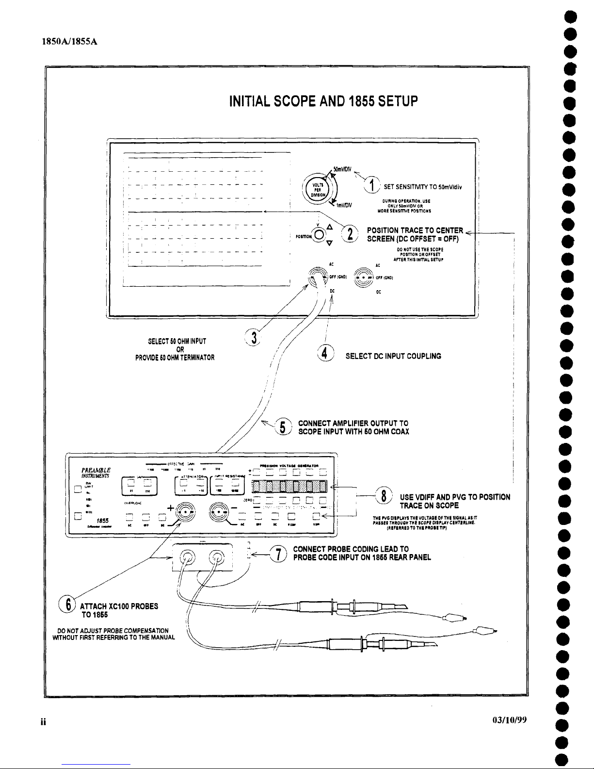
CONNECTING TO AND SETTING UP THE OSCIL-
LOSCOPE (See page ii)
Connect a 50 ohm coaxial cable between the AMPLIFIER
OUTPUT BNC on the 1850A/1855A rear panel and the
oscilloscope’s input connector. If the oscilloscope has I
megohm and 50 ohm input capability, select 50 ohms. If
the oscilloscope has only a one megohm input, terminate
the coaxial cable at the oscilloscope’s input with a 50 ohm
feed-through terminator. It is important that the
1850A/1855A be terminated by 50 ohms.
Set the oscilloscope deflection factor to 50mV/div. Set the
oscilloscope’s input coupling to GND or OFF and position
the trace to center screen. Do not move the oscilloscope
position setting after this initial set-up. Change the oscilloscope input coupling to DC.
1855A FRONT PANEL OPERATION
Change the power switch located on the 1850A/1855A’s
rear panel to 1 (on). The 1850 and 1855 will turn on
approximately 2 seconds.
All display indicators, including the red OVERLOAD light
and all segments in the Precision Voltage Generator display
will be lighted.
All controls except the Precision Voltage Generator (PVG)
display will next change to the state in which they were left
when the 1850A/1855A was last turned off. The PVG
display will show model number and firmware version
briefly. "’1855.11" means model 1855A, firmware version
03/10/99
1.1. The PVG display will then return to the voltage set
when the 1850A/1855A was last turned off.
During warm up, the 1855A may seem sluggish. Enter a
"I" in the least significant digit of the PVG display to kept
the microprocessor from constantly trying to autozero the
PVG before the instrument’s oven is up to temperature.
The PVG output will have an offset of up to 40mV during
this period. Before proceeding with the following exercise,
allow the 1855A to warm up for at least 7 minutes. Press
the PVG ZERO button before continuing.
ATTENUATOR AND GAIN OPERATION
Conduct the following exercise to familiarize yourself with
the 1850A/1855A: Connect the function generator output
to the +INPUT BNC connector and apply a sinewave of
50kHz and 0.5V peak amplitude. Push the DC button on
the 1850A/1855A’s +INPUT. The signal on the oscilloscope should be 2 divisions peak to peak in amplitude.
Adjust the oscilloscope’s sweep speed and trigger to display at least two complete cycles of the waveform.
Press the +1 ATTENUATOR button. The waveform’s
magnitude on the oscilloscope’s display will increase by a
factor of 10 and extend off the top and bottom of the
screen. The X1 light will be lighted in the EFFECTIVE
GAIN display. Reduce the function generator’s output until
the oscilloscope’s display is again 2 divisions peak to peak.
The overall sensitivity of the 1855A and the oscilloscope is
now 50mV/div.
Now press the XI0 GAIN button. Observe the following
changes: The +INPUT’s DC light will momentarily go out
and its OFF light will be lighted before returning to their
previous states. This momentary change is the result of the
1855A automatically adjusting its DC Balance (AUTO
ZERO). The XI0 light will be lighted in the EFFECTIVE
GAIN display and the display on the oscilloscope will
again extend off screen. The overall sensitivity of the
1855A and the oscilloscope is now 5mV/div.
3-1

General Operating Information -- 1850A/1855A
COMPARISON VOLTAGE OPERATION (VCOMP)
Leave the 1850A/Ig55A set up as in the previous exercise
or set as follows:
+INPUT
DC
-INPUT
OFF
BW LIMIT FULL
GAIN
XI0
ATTENUATOR +1
INPUT RESISTANCE
1M
PVG
+0.0000
COMPARISON or DIFFERENTIAL COMPARISON
EFFECTIVE GAIN
XI 0
¯ Function Generator output -- 50kHz 50mVpk sine
wave. connected to the 1850A/1855A’s + INPUT.
¯ Oscilloscope- Set at 50mV/div (equivalent to 5mV/div
with 1855A at X10 GAIN) and sweep adjusted for 2 to
cycles,
Under these conditions, the display on the oscilloscope will
extend offthe top and bottom of the screen.
Press the -INPUT’s Vco.~w button. This internally applies
the Precision Voltage Generator’s (PVG) output to the
1855A’s -INPUT and the OFF light goes out (the -INPUT connector is disabled). For the 1850A, connect
variable external voltage source capable of-10V to +IOV
range to the rear panel BNC marked OFFSET.
Note that for the 1855A, the rear panel OFFSET connector is an output which monitors the PVG voltage.
However, the 1850A OFFSET connector is an input accepting a range of-10V to +IOV. Serious damage will
result when the 1850A OFFSET connector is connected
to more than +__20 volts.
The positive and negative peaks of the waveform displayed
on the oscilloscope are (respectively) 10 divisions above
and below the display center line. Push the button above
the digit that is two places right of the decimal (lOmV)
the Precision Voltage Generator (PVG) until the positive
peak of the waveform appears in the oscilloscope’s display.
Continue incrementing and decrementing Precision Voltage
Generator’s digits until the peak of the waveform is at the
center line of the oscilloscope’s display. The number in the
Precision Voltage Generator display is the waveform’s
positive peak voltage.
For the 1850A, manually adjust the external voltage
source until the top of the waveform is at center line of
the oscilloscope’s display. Use a DVM to monitor the
external voltage source. The voltage at the center line
will equal the DVM reading.
3-2
The 1850A uses an OFFSET input range of only
-~15.5V to -15.5V (-,-10.0V to -10.0V in the VDnv~
mode). The offset is applied to the 1850A’s internal
amplifier’s negative input directly rather than through the
input attenuator. When the ATTENUATOR is set to
÷10 the effective offset is increased by a factor of 10.
Thus it takes only 9.3V applied to the rear panel OFFSET connector to offset 93V applied to the +INPUT
connector. Remember to apply this correction factor
when setting the ATTENUATOR to +10. An attenuat-
ing probe has the same effect, so using a +100 probe increases the effective offset range from +15,5V to
_+1550V. Remember, however that while the effective
offset is mathematically calculated in this fashion, many
probes are not capable of 1550 volts offset. Limit the
probe input to the voltage rating for the probe.
Press the + button in the Precision Voltage Generator. Observe that the negative peak of the signal is now at or near
the oscilloscope’s display center line. By incrementing and
decrementing the digits, the negative peak can be positioned to the oscilloscope’s display center line, Now the
number in the Precision Voltage Generator’s display is the
waveform’s negative peak voltage.
03/i 0/99
O
O
O
O
0
O
0
0
O
0
0
0
O
0
O
0
0
O
0
0
O
0
0
0
0
0
O
O
0
O
O
Q
0
0
O
e
O
O
O
t
O
O
O
a

0
0
0
0
0
0
0
0
0
0
0
0
0
0
0
0
0
0
0
0
0
0
0
0
0
0
0
0
0
0
0
0
0
0
0
0
0
0
0
0
0
0
0
0
Change the oscilloscope’s sensitivity from 50mV/div to
I 0mV/div. Overall sensitivity, including the 1850A/1855A,
is now lmV/div. Temporarily change the oscilloscope’s
input coupling from DC to GND (or OFF) and re-center the
trace to center screen using the oscilloscope’s position
control. Return its input coupling to DC. Now press the
XI0 button on the 1850A/1855A to invoke its AUTO
ZERO function. It is not necessary to disconnect the signal from the 1850A/1855A input to perform AUTO
ZERO. The 1850A/1855A automatically performs this
operation as part of the AUTO ZERO routine. (Note that
pressing the gain button that is already selected causes the
1850A/1855A to adjust its DC balance (invoke AUTO
ZERO), but does not change its gain.)
Change the Precision Voltage Generator’s reading to again
place the negative peak of the waveform at the oscilloscope’s center screen. Note that the PVG (Precision Voltage Generator) display represents the negative peak voltage
of the waveform with greater resolution.
The GAIN control affects the 1850A/1855A amplifier gain
but does not affect the offset range. The 1855A PVG display reflects this fact. The 1850A effective offset calculation is not affected by the GAIN setting.
Return the oscilloscope’s sensitivity to 50mV/div and press
the 1855A’s -INPUT OFF (or AC or DC) button. The
PVG will retain its setting and the display on the oscilloscope will be centered about the center line. Press the -INPUT’s VCOMP button again and observe that the Precision
Voltage Generator’s output is again connected to the minus
input of the 1855A’s -INPUT.
Following are a few observations on using the 1855A comparison voltage mode (VcoMP):
The negative input and its AC, OFF and DC coupling
are disabled. Instead of being a differential amplifier,
the 1855A becomes a differential comparator, it compares the voltage present at the +INPUT with the output of the Precision Voltage Generator and when they
are equal, the output of the 1855A is zero volts.
.
The value displayed by the Precision Voltage Generator indicates a waveform’s voltage, with respect to
ground, as it passes through the oscilloscope display’s
center line. It is very important that the oscilloscope’s
trace be positioned to center screen if an accurate
measurement is to be made using this method.
.
By using the 1855A in the comparison voltage mode
and the oscilloscope in a high sensitivity setting, highly
accurate voltage measurements can be made.
.
The Precision Voltage Generator can be used as a position control which allows the 1855A to operate in its
linear region.
03/10/99
General Operating Information -- !850A/1855A
DIFFERENTIAL OFFSET OPERATION (VcoMP)
Leave the 1855A set up as in the previous exercise or set it
up as follows:
+INPUT
DC
-INPUT
VcoMe
BW LIMIT
FULL
GAIN
Xl0
ATTENUATOR
+!
INPUT RESISTANCE
1M
PRECISION VOLTAGE GENERATOR
-0.0500*
COMPARISON or DIFFERENTIAL COMPARISON
EFFECTIVE GAIN
X10
*approximate, and apply approximately -0.05V to the
1850A rear panel OFFSET connector.
¯ Function Generator output -- 50kHz 50mVpk sine
wave connected to the +INPUT of the 1850A/1855A.
* Oscilloscope -- set at 50mV/div (equivalent to 5mV/div
with 1850A/1855A at XI0 GAIN) and sweep adjusted for
2 to 3 cycles.
¯ Externally trigger the oscilloscope on the function generator’s output (same signal as is applied to the I855A’s
+INPUT).
Under these conditions, the negative peak of the display on
the oscilloscope should be very near center screen. Adjust
the Precision Voltage Generator until the negative peak is
at center screen. For the 1850A, adjust the external voltage
source until the negative peak is at center screen.
Press the VDIFF button. This internally applies the output of
the Precision Voltage Generator to a point within the
1855A’s amplifier that facilitates a true differential offset.
Also note that the -INPUT coupling changed. The VcoMP
light v~ent out and the OFF light was lighted. In the line
under the Precision Voltage Generator display (COMPARISON or DIFFERENTIAL OFFSET), the COMPARISON light went out and the DIFFERENTIAL light
was lighted. This indicates that the Precision Voltage Generator will now be applied as a differential offset rather
than as a comparison voltage as in the previous exercise.
Both the +INPUT and the -INPUT inputs are now enabled, although the -INPUT is not in use at the moment.
Press the +_ button in the Precision Voltage Generator.
(With the 1850A, change the polarity of the external voltage source connected to the 1850A rear panel OFFSET
connector.) Observe that the negative peak of the signal is
now at or near the oscilloscope display’s center line. By
incrementing and decrementing the digits, the negative
peak can be positioned to the oscilloscope display’s center
line. Now the number in the Precision Voltage Generator’s
3-3

General Operating Information -- 1850A/1855A
display is the value of the waveform’s negative peak voltage. With the 1850A, the reading of the DVM attached to
the external voltage source will be the voltage at the oscil-
loscope center line.
Change the oscilloscope’s sensitivity from 50mV/div to
10mV/div. Overall sensitivity, including the ] 850A/1855A,
is now ImV/div. Temporarily change the oscilloscope’s
input coupling from DC to GND (or OFF) and re-center
the trace to center screen using the oscilloscope’s position
control. Return its input coupling to DC. Now press the
1850A/1855A XI0 button to invoke its AUTO ZER0
function. (Note that pressing the gain button that is already
selected causes the 1850A/1855A to adjust its DC balance,
i.e. invoke AUTO ZERO, but does not change its gain.)
Change the PVG (or external source in the 1850A case)
again place the negative peak of the waveform at the oscilloscope’s center line. Note that the Precision Voltage Generator’s display more accurately represents the negative
peak voltage of the waveform.
Return the oscilloscope’s sensitivity to 50mV/div and again
press the 1850A/1855A’s Vnwr button. The VmrF light will
extinguish and the oscilloscope display will be centered
about the center line. Notice that the 1855A PVG retains its
setting, but the output of the PVG is not applied to the amplifier. Press the VD~rr button again and observe that the
PVG’s output is reapplied internally to the 1855A amplifier.
Following are a few observations on using the differential
offset mode(Vmrr) of the 1850A/I 855A:
1. Both the positive and negative inputs (AC, OFF and
DC) are enabled and the 1850A/1855A remains a true differential amplifier.
2. The value displayed by the Precision Voltage Generator indicates a waveform’s differential voltage, with respect
to the -INPUT, as it passes through the oscilloscope display’s center line. It is very important that the oscilloscope’s trace be positioned to center screen if an accurate
measurement is to be made using this method. The voltage
applied to the 1850A’s OFFSET VOLTAGE input also
indicates the waveform’s differential voltage with respect
to its-INPUT.
3. By using the 1855A in the differential offset mode and
the oscilloscope in a high sensitivity setting, high resolution
voltage measurements can be made. The -INPUT is the
reference for these measurements.
4. The PVG can be used as a position control which al-
lows the 1855A to operate in its most linear region.
5. The PVG will retain its voltage when switching be-
tween Vco~lP and Vatvr if the voltage is less than 10.0
volts in magnitude, the maximum allowed for VDwF.
3-4
WHICH OFFSET MODE SHOULD BE USED?
The operations of the Comparison (Vco~w) and Differential
Offset modes (VDIFF) are quite similar. The Comparison
mode is easier to understand and has a wider range, 15.5
volts vs 10.0 volts. The Differential Offset mode provides
offset operation while allowing the 1855A to function as a
true differential amplifier.
For most applications, the Differential Offset (Vmrr) mode
has advantages over the Comparison (Vco,~w) mode. When
using the Comparison mode, the Precision Voltage Generator’s output is subtracted from the +INPUT, Except for
the PVG’s offset, operation is the same as a standard single-ended oscilloscope...only one 1850A/1855A input is
available. In the Differential Offset mode, the
1850A/1855A functions as a differential amplifier...both
+INPUT and -INPUT function. This allows the operator
to choose a measurement reference point other than ground.
Even in ground referenced measurements, signal degradation can be reduced by using the -INPUT probe to select a
ground reference point with the least noise. This method is
especially useful in eliminating hum and noise from ground
loops.
There is one instance in which the Differential Offset
(VDIvr) mode might result in more noise. Magnetic pick-up
is proportional to the area between the probes. If twisting
the probe leads together is not sufficient to reduce magnetic
pick-up, the Comparison Offset (Vcos~r) mode may
preferable.
Because the Comparison Offset mode uses the CMRR of
the 1850A/1855A while the Differential Offset mode uses
an internal amplifier, the Comparison Offset mode is
slightly more accurate.
The Differential Offset (Vnjrr) mode is usually the mode
choice if the wider range or higher accuracy of the Comparison (VcoMe) mode is not needed.
OPERATOR TRAPS TO AVOID
There are a few situations the operator of either the 1850A
or 1855A should be aware of to avoid some potential
measurement traps.
EXCEEDING COMMON MODE RANGE
The 1850A and 1855A Differential Amplifiers have the
largest common mode range available for this type of amplifier and are very good at measuring small differences
between two large signals. However, care still must be
taken not to allow a large common mode signal to exceed
the available common mode range.
The maximum common mode range is ±15.5 volts when a
signal is applied directly (÷1 ATTENUATOR and no
probes) to the 1850A/1855A’s + and -INPUTS.
03/10/99
0
0
0
0
0
0
0
0
0
0
0
0
0
0
0
0
0
0
0
I
0
0
0
0
0
0
0
0
0
0
0
0
0
0
0
0
0
0
0
0
e
I

0
0
0
0
0
0
0
0
0
0
0
0
0
0
0
0
0
0
0
0
0
0
0
0
0
0
0
0
0
0
0
0
0
0
0
0
0
Attenuating the input signal extends the common mode
range by the same factor as the attenuation. Pressing the
+10 ATTENUATOR button increases the common mode
range to ±155 volts, and using a probe with a +10 attenuation factor will too. The effect of the internal ÷10 AT-
TENUATOR and the attenuation factor of probes is multi-
plied just as the signal is attenuated. For example, using
the amplifier’s ÷10 ATTENUATOR with a probe having a
+100 attenuation factor (total attenuation of + 1000) results
in a common mode range of 15,500 volts. In this case, the
probe’s maximum voltage rating probably limits the maxi-
mum common mode input voltage.
The gain setting of the amplifier has no effect on common
mode range; it is the same in XI0 GAIN as it is in XI.
When making measurements on circuits that are line referenced, use enough total attenuation to keep the peak voltage at the amplifier input below 15.5 volts. The US
power-line can exceed 170 peak volts and therefore at
least a total attenuation of ÷100 should be used. Line
voltages in some other countries are larger but their peak
voltages do not exceed the 1550 volt common mode range
that a +100 attenuation factor provides.
MOVING THE OSCILLOSCOPE POSITION SETTING
AWAY FROM CENTER SCREEN
When operating the 1850A/1855A with a scope, it is very
important to set the oscilloscope’s position and/or offset
control to center screen, There are a couple of reasons for
this.
First, the linear portion of the 1850A/1855A’s ±500mV
output range is centered around zero volts. As the
1850A/1855A approaches its limits, the output signal will
be distorted. Moving the oscilloscope’s position control
way from center screen can allow these distortions to
appear on the oscilloscope’s screen where they may be
mistaken for part of the displayed signal.
Second, proper operation of the 1855A’s Precision Voltage
Generator (PVG) depends on the operator knowing the
location of zero volts on the display. The readout in the
PVG is designed to display the voltage of the signal as it
crosses the center line of the oscilloscope screen. If the
oscilloscope’s position or offset control has been moved,
incorrect readings could result.
When the 1855A is controlled with the ProBus interface
(using the REMOTE connector on the 1850A/1855A rear
panel), the offset control on the oscilloscope controls the
1855A PVG. The PVG display will read the offset set from
the oscilloscope front panel.
When the 1850A is controlled with the ProBus interface, an
external source must be used to control the vertical trace
position:
03/10/99
General Operating Information -- 1850A11855A
USING SCOPE AT GREATER THAN 50mV/div (e.g.
200m V/div)
"I know the input to the 1850A/1855A is a sinewave, but I
am seeing a squarewave on the oscilloscope." This comment is the result of the operator setting the oscilloscope
sensitivity to something less than 50mV/div. If the oscilloscope sensitivity ’is set to 200mV/div, the 1850A/1855A
will limit at 2%_ divisions above and below center screen
(zero volt point if the oscilloscope’s position control is
properly set). Thus, a sinewave large enough to overdrive
the 1850A/1855A will appear as a squarewave on the os-
cilloscope.
The 1850A/1855A is designed to cleanly limit the output
signal to ±500inV. The 1850A/1855A is designed to recover very quickly once its input signal level decreases
sufficiently to allow the amplifier to return to its linear
range. The 1850A/1855A will recover from overdrive to
its full accuracy much more quickly than most oscillo-
scopes.
If the 1850A/I 855A did not limit the signal at +_.500mV, it
would be of no help to the oscilloscope in viewing large
signals.
Keeping the oscilloscope’s position at center screen and
using oscilloscope sensitivities between 50mV/div and
l mV/div (or the oscilloscope’s most sensitive setting) will
insure good signal integrity. When the displayed signal
contains mostly low frequency components, the operator can use the oscilloscope’s 100mV/div setting to allow
large signals to he completely shown on screen.
FAILURE TO TERMINATE THE AMPLIFIER IN 50
OHMS
"All the signals displayed on my oscilloscope seem to be
twice as large as they should be." This comment results
from not having the output of the 1850A/1855A properly
terminated into 50 ohms. The 1850A/1855A output impedance is 50 ohms. The cable connecting the
1850A/1855A to the oscilloscope or spectrum analyzer
should be 50 ohms and be terminated with a 50 ohm load.
If the termination at the end of the connecting coaxial cable
is missing, the amplifier will not be properly terminated.
Several things occur if the external termination is missing.
First, the output isn’t properly terminated for all frequencies resulting in poor frequency and transient response. For
most signals this distortion will be minor, except when the
1855A’s 1 MHz and 20 MHz bandwidth limit filters are
used. These filters will ring when not properly terminated.
Failure to use a 50 ohm coaxial cable will adversely affect
the transient response of the 20MHz filter even though the
termination impedance is 50 ohms.
3-5

General Operating Information -- 1850A/1855A
Second, the gain of the amplifier will be twice that indicated by the front panel settings. The 1855A’s EFFECTIVE GAIN indicator will be offby a factor of two.
In some measurements, the operator can take advantage of
this increased gain if the problems caused by not terminat-
ing the output are fully understood and taken into account.
The 1850A/1855A maximum output is limited to _+_I.0V
when the output is terminated with 1 megohm.
3-6
03/10/99
0
0
0
0
0
0
0
0
0
0
0
0
0
0
0
0
0
0
0
0
0
0
0
0
0
0
0
0
0
0
0
0
0
0
0
0
0
0
0
0
0
0
0
m

Copyright© 1999, Preamble Instruments, Inc. All rights reserved.
Printed in U. S. A.
Preamble Instruments, Inc. products are covered by U. S. and foreign patents, issued or pending.
Specification changes reserved. Information contained in this publication supersedes all previously published material.
Preamble Instruments, Inc. and
J~ ,,OmUtMBlJlregistered trademarks.
" V IIME’II~JM|IWT
WARRANTY
Preamble Instruments warrants the products it manufactures and sells to be free of defects in materials and workmanship for
a period of three years, (one year for passive probes and probe accessories). Preamble lnswuments will repair or replace,
its option, any product which proves defective within the warranty period.
To obtain warranty service, the customer must contact Preamble Instruments within the warranty period to obtain a Return
Material Authorization. The customer shall be responsible for the proper packaging, insurance and shipping charges for the
return of the product to Preamble Instruments. Preamble Instruments will pay the shipping charges for the return of the
product to the customer.
This warranty does not apply to damage resulting from the improper use or abuse of the product. The warranty also excludes
any damage resulting from repair or modifications of the product which were not performed by Preamble Instruments or its
authorized service facility.
This warranty is exclusive and no other warranty shall be made by Preamble Instruments or its representatives,
express or implied. Preamble Instruments disclaims any implied warranty of fitness for use. Preamble Instruments’
sole responsibility under the foregoing conditions of this warranty is the repair or replacement of products. Preamble
Instruments and its representatives will not be liable for any special, indirect, incidental, or consequential damages
resulting from the use of this product.
PREAMBLE INSTRUMENTS, Inc.
P.O. Box 6118
Beaverton, OR 97007-0118
U.S.A.
(503) 646-2410
FAX: (503) 646- i 604
www.preamble.com
e
e
e
e
e
e
e
e
i
e
e
o
o
o
o
e
e
e
o
o
o
o
e
e
e
e
o
o
o
o
o
o
o
o
o
o
o
o
o
o
o
o
o
A
 Loading...