

Page 1
-,~ ~OREAMBLE
-
VIINSTRUMENTS
1820/1822
DIFFERENTIAL AMPLIFIER
OPERA TOR’S
MANUAL
Revision D
August 1999
Page 2
Table of Contents
Section 1
Specifications
Introduction .............................................................................
1 - 1
1820/1822 Specifications ........................................................
1-2
Nominal Characteristics ..........................................................
1-3
Warranted and Typical Characteristics .................................... 1-4
Environmental and Physical Characteristics ............................
1-5
Section 2
Operating Instructions, Controls and Indicators
Front Panel ..............................................................................
2-1
Rear Panel ...............................................................................
2-4
Oscilloscope Settings ...............................................................
2-5
Model 1820 Operation .............................................................
2-6
Section 3
General Operating Information
Getting Started .........................................................................
3-1
1822 Front Panel Operation .....................................................
3-1
Comparison Voltage Operation ...............................................
3-2
Differential Offset Operation ..................................................
3-3
User Traps to Avoid ................................................................
3-4
Section 4
Performance Verification
Introduction ............................................................................. 4-1
Test Equipment Required ........................................................
4-2
Preliminary Procedure .............................................................
4-3
Procedure .................................................................................
4-3
1820/1822 Test Record ..........................................................
4-11
0
0
0
0
0
0
0
0
0
0
0
0
0
0
0
0
0
0
0
0
0
0
0
0
0
0
0
0
0
0
0
0
0
0
0
0
0
0
0
0
0
0
0
0
Page 3
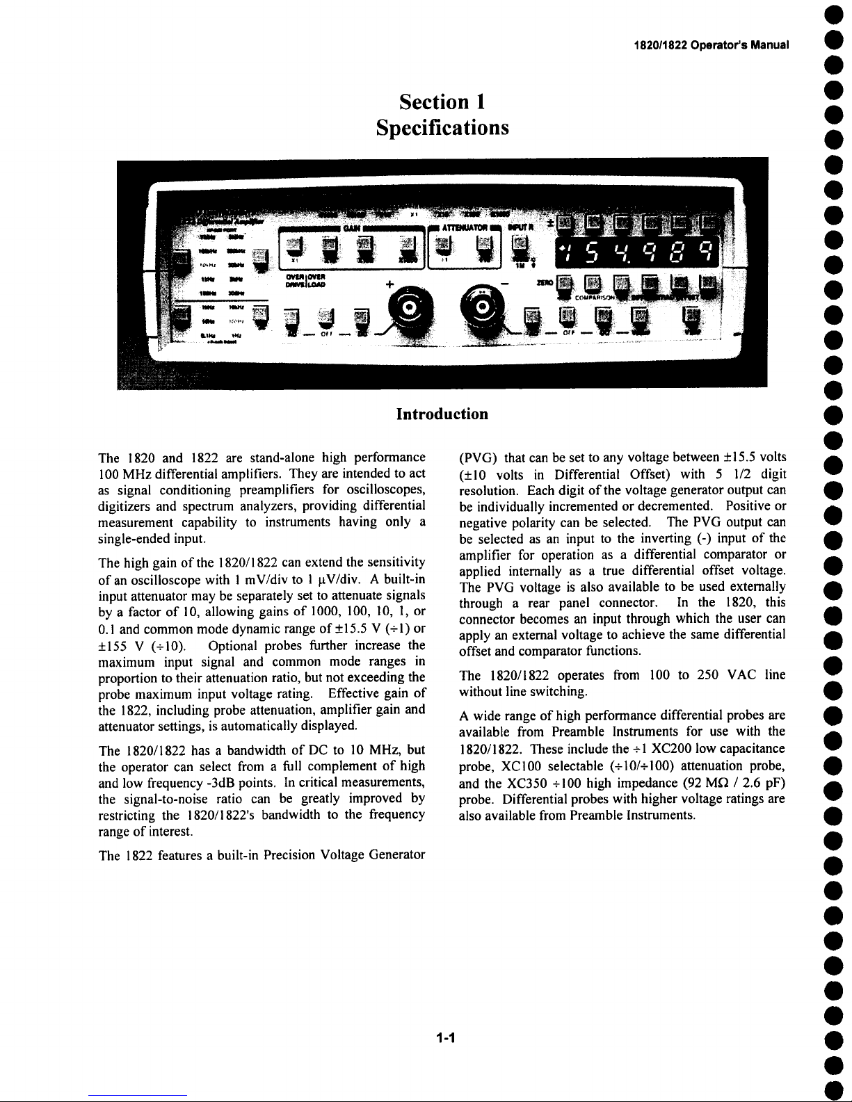
Section 1
Specifications
Introduction
182011822 Operator’s Manual
The 1820 and 1822 are stand-alone high performance
100 MHz differential amplifiers. They are intended to act
as signal conditioning preamplifiers for oscilloscopes,
digitizers and spectrum analyzers, providing differential
measurement capability to instruments having only a
single-ended input.
The high gain of the 1820/1822 can extend the sensitivity
of an oscilloscope with 1 mV/div to 1 laV/div. A built-in
input attenuator may be separately set to attenuate signals
by a factor of 10, allowing gains of 1000, 100, 10, 1, or
0.1 and common mode dynamic range of +15.5 V (+1)
+155 V (+10). Optional probes further increase the
maximum input signal and common mode ranges in
proportion to their attenuation ratio, but not exceeding the
probe maximum input voltage rating. Effective gain of
the 1822, including probe attenuation, amplifier gain and
attenuator settings, is automatically displayed.
The 1820/1822 has a bandwidth of DC to 10 MHz, but
the operator can select from a full complement of high
and low frequency -3dB points. In critical measurements,
the signal-to-noise ratio can be greatly improved by
restricting the 1820/1822’s bandwidth to the frequency
range of interest.
The 1822 features a built-in Precision Voltage Generator
(PVG) that can be set to any voltage between +15.5 volts
(+10 volts in Differential Offset) with 5 1/2 digit
resolution. Each digit of the voltage generator output can
be individually incremented or decremented. Positive or
negative polarity can be selected. The PVG output can
be selected as an input to the inverting (-) input of the
amplifier for operation as a differential comparator or
applied internally as a true differential offset voltage.
The PVG voltage is also available to be used externally
through a rear panel connector. In the 1820, this
connector becomes an input through which the user can
apply an external voltage to achieve the same differential
offset and comparator functions.
The 1820/1822 operates from 100 to 250 VAC line
without line switching.
A wide range of high performance differential probes are
available from Preamble Instruments for use with the
1820/1822. These include the +1 XC200 low capacitance
probe, XCI00 selectable (+10/+100) attenuation probe,
and the XC350 +100 high impedance (92 M~ / 2.6 pF)
probe. Differential probes with higher voltage ratings are
also available from Preamble Instruments.
1-1
Page 4

1820/1822 Operator’s Manual
1820/1822 Specifications
Except where otherwise noted, the following specifications apply to model 1820, 1822,
1820-PR2 and 1822-PR2
Differential Amplifiers.
The specifications are valid for instruments when the following conditions have been met:
The instrument is being operated from a power source which meets the line voltage and frequency specifications.
The instrument has been operating for at least 30 minutes in an environment which is within the operating
environmental specifications.
¯
The instrument has been calibrated within the last 12 months. Calibration was performed in a controlled environment
of 25 +5°C.
Nominal Characteristics
Nominal characteristics describe parameters and attributes which have are guaranteed by design, but do not have
associated tolerances.
General
Input Configuration:
True Differential, + and - Inputs.
Precision Voltage Generator (1822 and 1822-PR2
models), or external offset reference source (1820
and 1820-PR2 models) can be selected as - input
source in VCOMP mode.
Offset Capability
The Precision Voltage Generator (1822 and 1822PR2 models), or external offset reference source
(1820 and 1820-PR2 models) can be used
provide true differential offset.
+ Input Coupling Selections
- Input Coupling Selections
Input Connectors
AC, Off (Precharge),
AC, Off (Precharge), DC, VcouP
BNC. + Input incorporates Probe Attenuation
Coding sensing connector (1822 Only).
Maximum Non-Destruct Input Voltage
Withstands up to +250 V.
Automatic input disconnect with manual reset
Output Configuration
Output Impedance
Intended Output Load
Output Connector
Amplifier Gain
Input Attenuation
Bandwidth Limit Filters (Upper Limit)
Single Ended, Ground referenced.
50
50f)
BNC
X1, X10, XI00, or X1000
+1 or +10
100 Hz, 300 Hz, 1 KHz, 3 KHz, 10 KHz,
30 KHz, 100 KHz, 300 KHz, 1 MHz, 3 MHz
Bandwidth Limit Filters (Lower Limit)
Bandwidth Limit Filter Characteristics
Autobalance
0.1 Hz, 1 Hz, 10 Hz, 100 Hz, 1 KHz, 10 KHz
Single pole, 6 dB/octave
Amplifier initiates an automatic balance cycle
when either gain button is depressed.
Effective Gain Indicator
(1822 and 1822-PR2 models only)
LEDs indicate the effective gain by factoring
Probe Attenuation, Attenuator and Gain settings.
(Probes must have coding connectors.
+ 1, + 10, + 100, and + 1000 probes are
recognized.)
1-2
Page 5

182011822 Operator’s Manual
Nominal Characteristics (continued)
Dynamic Ranges
Maximum Differential Linear Input:
X 1000 Gain, + 1 Attenuator
X100 Gain, +1 Attenuator
X 10 Gain, - 1 Attenuator
XI Gain, +l Attenuator
XI000 Gain, +10 Attenuator
X 100 Gain, + I 0 Attenuator
X 10 Gain, + ! 0 Attenuator
XI Gain, +10 Attenuator
~
+5 mV
j
+50 mV
1
+0.5 V
I
+5 V
I
_+50 mV
l
¯ +0.5 V
~
+5 V
t
+50 V
Maximum Common Mode Input
+ 1 Attenuator
+ 10 Attenuator
1
+15.5 V
l
¯ +155 V
Differential Offset Range (VD~FV Mode)
(referred to input)
X 10, X 100, X 1000 Gain, + 1 Attenuator
X 1 Gain, + ! Attenuator
Xi0, X100, XI000 Gain, +10 Attenuator
X ! Gain, +l 0 Attenuator
I
¯ +! V
1
¯ +!0 V
l
±10 V
I
±100 V
Comparison Offset Range (VcoMP Mode)
(referred to input)
+ 1 Attenuator
+ 10 Attenuator
Output Range
I
_+15.5 V
I
¯ +i55 V
Limitedto _+5 V into 50 ~ load
t Voltages are referred amplifier input connector. Multiply by probe attenuation factor to obtain value refer to probe
input. (e.g. _+50 mV1 becomes +0.5V at the probe tip when using a +10 probe.)
Precision Voltage Generator (1822 and 1822-PR2 models
Output Range
Resolution
Control
Reference Type
Output Routing
Autozero
Power Requirements
Line Voltage Range
Line Frequency Range
only)
±15.5 V
1 O0 p.V
Individual increment and decrement buttons for
each digit. Digit carries over to next decade.
Oven stabilized buried Zener
Can be applied to - input and available at rear
panel BNC connector.
Removes output offset when 0.0000 volts is
selected and periodically thereafter.
100 - 250 VAC
48 - 66 Hz
1-3
Page 6

1820/1822 Operator’s Manual
Warranted Characteristics
Warranted characteristics describe parameters which have guaranteed performance.
provided in the Performance Verification Procedure for all warranted specifications.
Unless otherwise noted, tests are
Gain Accuracy
+1% + Uncertainty of termination resistance
Bandwidth (- 3dB)
X1 or XI0 Gain
X 100 Gain
X 1000 Gain
Rise Time (XI or X10 Gain)
>10 MHz
>2.5 MHz
>1 MHz
<35 ns (Calculated from Bandwidth)
Common Mode Rejection Ratio
(X 1 or X 10 Gain)
70 Hz
100 KHz
1 MHz
Precision Voltage Generator Accuracy
>100,000:1 (100 dB)
>100,000:1 (100 dB)
>1,000:1 (60 dB)
0.05% of reading + 500 ~tV (15° to 45° C.)
Typical Characteristics
Typical characteristics describe parameters which do not have guaranteed performance. Tests for typical characteristics
are not provided in the Performance Verification Procedure.
Input Resistance
+1 Attenuator
1 MF2 or 100 Mr2
1 Mr2 only with attenuating probe
+ 10 Attenuator
Input Capacitance
AC Input Coupling Capacitance
+ 10 Attenuator Accuracy
DC Drift (X10 Gain, referred to input)
Input Leakage Current
1 Mr2
20 pF
0.1 ~tF
0.05%
50 ~tVPC
<10 pA (0° - 45° C.)
(X 1 or X 10 Gain, + 1 Attenuator)
Differential Offset Accuracy
X i 0, X 100, X 1000 Gain, + 1 Attenuator
XI Gain, +1 Attenuator
X 10, X 100, X 1000 Gain, + 10 Attenuator
XI Gain, +10 Attenuator
Precision Voltage Generator Temperature
O. 1% + 50 laV
2
0.1% + 500 ~tV
2
O. 15% + 500 ~tV
2
O. 15% + 5 mV
<5 mVPC of full scale
2
Coefficient (1822 and 1822-PR2 models)
Power Consumption
26 W, ~ 36 VA (1820 and 1822)
52 W, ~ 72 VA (1820-PR2 and 1822-PR2)
2 Voltages are referred amplifier input connector. Multiply by probe attenuation factor to obtain value refer to probe
input. (e.g. 0.1% + 50 ~tV2 becomes 0.1% + 500 laV at the probe tip when using a +10 probe.)
Page 7
1820/1822 Operator’s Manual
Environmental Characteristics
The Environmental Characteristics are tested to specification MIL-T28800D Class 5.
performance verification of environmental characteristics is required.
Refer to this specification if
Temperature Range, operating
Temperature Range, non-operating
0° - 50° C.
-40° - 75° C.
Physical Characteristics
Height
Width
Depth
Weight
Shipping Weight
7.29 cm (2.87") (1820 and 1822 models)
8.75 cm (3.4") (1820-PR2 and 1822-PR2 models)
21.2 cm (8.36") (1820 and 1822 models)
43.9 cm (17.3") (1820-PR2 and 1822-PR2 models
without rack mounting ears installed)
23.2 cm (9.12") (1820 and 1822 models)
42.5 cm (16.7")(1820-PR2 and 1822-PR2 models)
2.15 kg (4 Ibs. 12 oz.) (1820 and 1822 models)
9.5 kg (21 lbs.) (1820-PR2 and 1822-PR2 models)
3.12 kg (6 lbs. 14 oz.) (1820 and 1822 models)
11.3 kg (25 lbs.) (I 820-PR2 and 1822-PR2 models)
Compliances
EC Declaration of Conformity
Designed to comply with EN61010-1 : 1993
Installation Category l, 42.2V, pollution degree 1.
Conforms to Low Voltage Directive 73.72 EEC for
product safety.
1-5
Page 8
1820/1822 Operator’s Manual
Section 2
Operating Instructions, Controls, and Indicators
Front Panel
Attenuator
Signals connected to the +INPUT and the -INPUT are
connected either directly to the 1820/1822’s amplifier
inputs or to the input attenuators. The input attenuators
are passive networks which divide each signal by ten.
In ÷1 mode the front panel input connectors are directly
connected to the 1820/1822 amplifier’s differential inputs.
In ÷10 mode each front panel input connector is
connected to a passive 1 Mr2 attenuator. The attenuator
output is connected to the 1820/1822 amplifier’s
corresponding differential input. The signal at each input
is attenuated by a factor of ten.
Gain
The 1820/1822 amplifier gain (amplification) is selectable
XI, XI0, XI00 and XI000. The amplified signal appears
at the rear panel AMPLIFIER OUTPUT connector.
A signal connected to the +INPUT will maintain its
polarity at the output connector. A signal connected to
the -INPUT will be inverted in polarity.
Proper gain is obtained when the 1820/1822 drives a 50
load such as an oscilloscope with input impedance set to
50 fL An oscilloscope with only 1 Mr2 input impedance
available should have a 50 f2 coaxial termination placed
on its input connector. The ! 820/1822 is then connected
to the oscilloscope through the coaxial termination.
The amplifier gain and the input attenuator are
individually selectable to provide versatility. For
example, the comparison voltage range is changed from
+15.5000 to ±155.000 volts by changing the
ATTENUATOR from +1 to ÷10. The overall gain can
still be set to 100, 10, 1 or 0.1 by selecting the GAIN
mode, XI000, X100, XI0 or XI, as desired.
Autobalance is a feature invoked when any gain button is
pushed, even if a different gain is not selected.
Autobalance momentarily sets the INPUT COUPLING
to OFF and determines the offset necessary to set the
output at 0 volts within about 25~tV. During this process
the front panel input coupling controls are unresponsive.
When finished, the INPUT COUPLING returns to its
previous mode. Autobalance usually takes less than one
second. This handy feature allows the operator to DC
balance the 1820/1822 simply by pushing the GAIN
button which is already illuminated. When changing
gains, the Autobalance feature is automatically invoked,
freshly adjusting the amplifier’s DC balance.
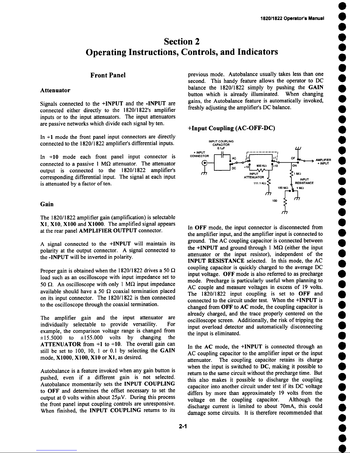
+Input Coupling (AC-OFF-DC)
INPUT COUPLING
CAPACITOR
+ INPUT
CONNECTOR [----11--7 AC ~11 I+1[
0.I~ .......
l [ r--- , ¯
10 900 K~ +10
ATTENUATOR
11111
i
In OFF mode, the input connector is disconnected from
the amplifier input, and the amplifier input is connected to
ground. The AC coupling capacitor is connected between
the +INPUT and ground through 1 M~ (either the input
attenuator or the input resistor), independent of the
INPUT RESISTANCE selected. In this mode, the AC
coupling capacitor is quickly charged to the average DC
input voltage. OFF mode is also referred to as precharge
mode. Precharge is particularly useful when planning to
AC couple and measure voltages in excess of 19 volts.
The 1820/1822 input coupling is set to OFF and
connected to the circuit under test. When the +INPUT is
changed from OFF to AC mode, the coupling capacitor is
already charged, and the trace properly centered on the
oscilloscope screen. Additionally, the risk of tripping the
input overload detector and automatically disconnecting
the input is eliminated.
In the AC mode, the +INPUT is connected through an
AC coupling capacitor to the amplifier input or the input
attenuator. The coupling capacitor retains its charge
when the input is switched to DC, making it possible to
return to the same circuit without the precharge time. But
this also makes it possible to discharge the coupling
capacitor into another circuit under test if its DC voltage
differs by more than approximately 19 volts from the
voltage on the coupling capacitor. Although the
discharge current is limited to about 70mA, this could
damage some circuits. It is therefore recommended that
2-1
Page 9
182011822 Operator’s Manual
the +INPUT COUPLING first be changed to OFF
(precharge) when measuring a new circuit point. This
will safely recharge the AC coupling capacitor in less
than 0.3 seconds. The value of the AC coupling capacitor
is 0.1 laF.
DC and low frequencies are attenuated by the AC
coupling capacitor and the input resistance. With the
ATTENUATOR set to +10, or set to +1 with the INPUT
RESISTANCE set to 1 Mr2, the low frequency cut off
(-3dB point) is approximately 1.6Hz, lower than most
oscilloscopes by a factor of 5. When the input attenuator
is set to +1, the INPUT RESISTANCE may be set to
100 M~, and the -3dB point is 0.016Hz. This extremely
low frequency cut off is often handy in observing low
frequency noise riding on large (up to 400 volts)
voltages.
In the DC mode, the +INPUT connector is connected to
the amplifier either directly or through the input
attenuator, and the AC and DC attenuation are the same.
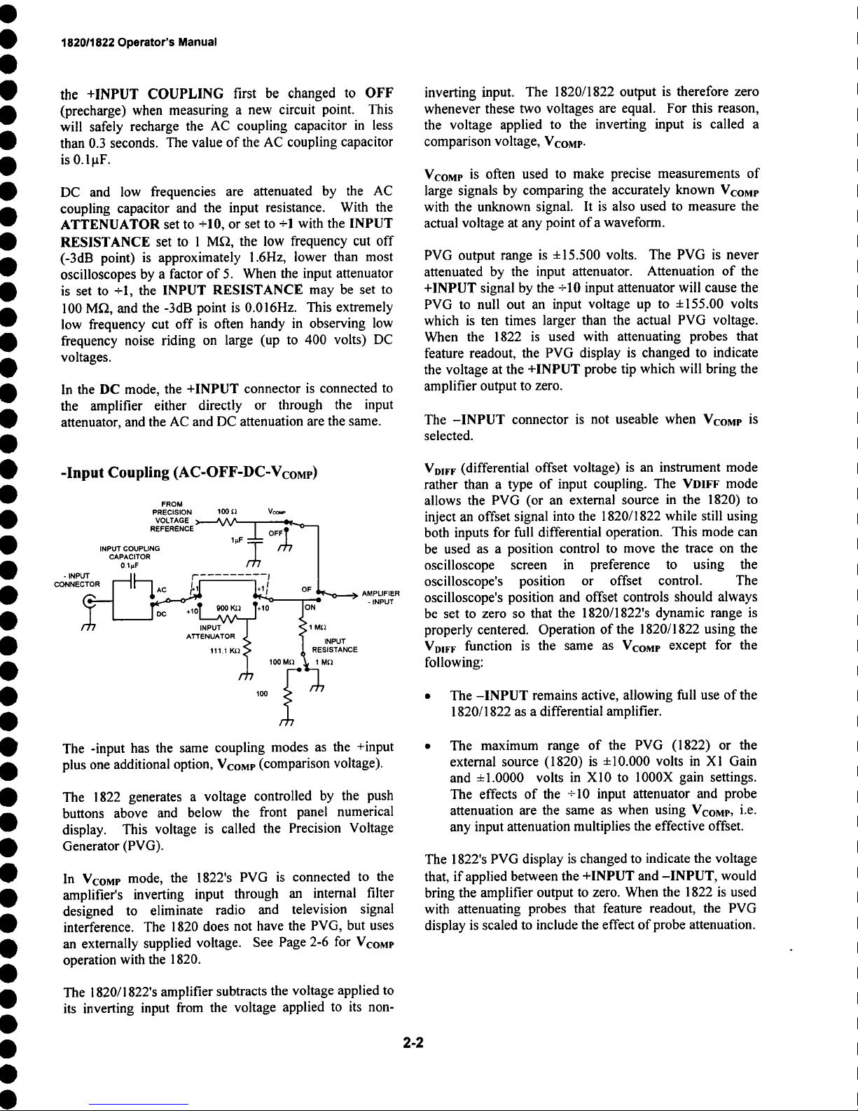
-Input Coupling (AC-OFF-DC-VcoMP)
PRECISION
VOLTAGE )-
REFERENCE
INPUT COUPLING
CAPACITOR
- INPUT
CONNECTOR
~ I.~ /-" .........
l r Ac
("~ I1~
I
~ -+lOT 900 KI] ~*10-
/7/ INPUT
FROM
100 II Vcoup
~
I I
H
ATTENUATOR
111.1 KI2
v A_
/ (’O--I
1 I / / I
I
]
M OF L
~______.~..~’~O ). AMPLIFIER
I
ION-
~1 Mr1
RESISTANCE
100 Mfl fl
INPUT
-INPUT
inverting input. The 1820/1822 output is therefore zero
whenever these two voltages are equal. For this reason,
the voltage applied to the inverting input is called a
comparison voltage, VcoMP.
VcoMP is often used to make precise measurements of
large signals by comparing the accurately known Vcome
with the unknown signal. It is also used to measure the
actual voltage at any point ofa waveform.
PVG output range is +15.500 volts. The PVG is never
attenuated by the input attenuator. Attenuation of the
+INPUT signal by the -10 input attenuator will cause the
PVG to null out an input voltage up to ±155.00 volts
which is ten times larger than the actual PVG voltage.
When the 1822 is used with attenuating probes that
feature readout, the PVG display is changed to indicate
the voltage at the +INPUT probe tip which will bring the
amplifier output to zero.
The -INPUT connector is not useable when Vcome is
selected.
VDIFF (differential offset voltage) is an instrument mode
rather than a type of input coupling. The VBIFF mode
allows the PVG (or an external source in the 1820)
inject an offset signal into the 1820/1822 while still using
both inputs for full differential operation. This mode can
be used as a position control to move the trace on the
oscilloscope screen in preference to using the
oscilloscope’s position or offset control. The
oscilloscope’s position and offset controls should always
be set to zero so that the 1820/1822’s dynamic range is
properly centered. Operation of the 1820/1822 using the
VD|FF function is the same as VCOMP except for the
following:
The -input has the same coupling modes as the +input
plus one additional option, VcoMv (comparison voltage).
The 1822 generates a voltage controlled by the push
buttons above and below the front panel numerical
display. This voltage is called the Precision Voltage
Generator (PVG).
In VCOMP mode, the 1822’s PVG is connected to the
amplifier’s inverting input through an internal filter
designed to eliminate radio and television signal
interference. The 1820 does not have the PVG, but uses
an externally supplied voltage. See Page 2-6 for VcoMv
operation with the 1820.
The 1820/i 822’s amplifier subtracts the voltage applied to
its inverting input from the voltage applied to its non-
¯
The -INPUT remains active, allowing full use of the
1820/1822 as a differential amplifier.
The maximum range of the PVG (1822) or the
external source (1820) is ±10.000 volts in XI Gain
and ±1.0000 volts in X10 to 1000X gain settings.
The effects of the +10 input attenuator and probe
attenuation are the same as when using VCOMP, i.e.
any input attenuation multiplies the effective offset.
The 1822’s PVG display is changed to indicate the voltage
that, if applied between the +INPUT and -INPUT, would
bring the amplifier output to zero. When the 1822 is used
with attenuating probes that feature readout, the PVG
display is scaled to include the effect of probe attenuation.
2-2
Page 10
1820/1822 Operator’s Manual
Input Resistance
When the input ATTENUATOR is set to -1 and no
attenuating probe is connected, the input resistance can be
increased from 1 Mr2 to 100 Mr2 by pressing the
100M/IM button. This is advantageous when measuring
high impedance circuits or when AC coupling is needed
with a very low frequency cut off. When the input
ATTENUATOR is set to -10 or an attenuating probe
with readout capability is attached, 1 Mr2 (IM) input
resistance is automatically selected.
Unbalanced source impedances can have an adverse
effect on common mode rejection. For example, a
differential source with impedances of 1000 and 2000 [2,
each loaded with 1 M£2 will have a common mode
rejection ratio (CMRR) of 1000 to 1. The common mode
rejection ration can be improved to 100,000 to 1 by using
100 M~ input resistance.
This limitation is also apparent when trying to make
accurate measurements using VCOMP. A 10.000 volt
reference with a 1000 f2 output impedance will be
reduced to 9.9900 volts by the 1820/1822 1 M~ input
resistance, introducing a 10 mV error in the measurement.
Increasing the input resistance to 100 M~ decreases this
error to 100~tV.
frequency -3 dB points are 3MHz, I MHz, 300kHz,
100kHz, 30kHz, 10kHz, 3kHz, IkHz, 300Hz and 100Hz.
Selections for the lower -3 dB points are 0.1Hz, IHz,
10Hz, 100Hz, lkHz and 10kHz. These filters make it
possible to improve the signal-to-noise ratio when making
measurements on microvolt magnitude signals.
Precision Voltage Generator (1822 Only)
The PVG generates the voltage which is used in the
VCOMP and VDWF modes and appears at the rear panel
PRECISION VOLTAGE GENERATOR OUTPUT
connector.
Above each digit is a push button which increments the
corresponding digit by one when pushed. When held, the
digit continues to increment, eventually incrementing the
next higher digit.
Similarly, below each digit is a push button which
decrements the corresponding digit.
The 4- button above the left-most digit changes the PVG
output polarity. The ZERO button below the left-most
digit sets the output to zero and invokes the Autozero
function.
Oscilloscope inputs have a small input current which can
cause an offset when measuring high impedance circuits.
The offset can be observed by opening and shorting the
input to ground. The 1820/1822 has a temperaturecompensated input current pull away (cancellation) which
works in both the 1 M~ and 100 Mr2 INPUT
RESISTANCE modes. Its input offset current is
considerably less than that of most oscilloscopes.
Effective Gain (1822 Only)
Seven lights (LEDs) across the top of the 1822 front panel
indicate the total gain from the instrument input to output.
When the X1 light is lighted, the overall amplifier voltage
gain (amplification) is unity. Similarly, XI0 indicates
overall amplification of ten times. +10 indicates the
voltage amplification is 0.1, and so forth.
When Preamble Instruments or other encoded probes are
properly used, the effective gain includes the probe’s
attenuation factor.
Upper and Lower -3 dB Points
The 1820/22 allows the user to select both the upper and
lower frequency -3 dB points. Selections for the high
Autozero resets the PVG output to zero to eliminate any
drift which may have occurred in the PVG due to low
frequency noise, or long term drift. Autozero is invoked
each time the ZERO button is pressed and re-invoked
approximately every minute thereafter. This is useful
when the instrument has been unplugged and a cold start
is required.
Overdrive (yellow)
When a signal is applied to either input of the 1820/1822
that exceeds its ±15.5 volt input range the yellow
OVERDRIVE indicator is lighted. The light remains on
as long as the input remains larger than the linear range.
The linear range is multiplied by the ATTENUATOR
factor and by the use of an attenuating probe.
The yellow OVERDRIVE light is intended to warn the
user of potentially distorted waveforms.
Overload (red)
When a signal which could damage to the 1820/1822 has
been applied to either input connector, the 1820/1822
protects itself by disconnecting the signal. The input
2-3
Page 11

182011822 Operator’s Manual
coupling mode changes to OFF, and the red
OVERLOAD light is turned on.
The 1820/1822 is reset and the OVERLOAD light goes
out when any of the input coupling modes is selected.
When the ATTENUATOR is set to -1, a signal of
approximately ±19 volts will cause the input to draw
current and the OVERLOAD light to come on.
Transients too rapid to he disconnected by the input
coupling relay will draw up to about 70mA of input
current. Inputs in excess of 250 volts may cause
permanent damage to the i 820/1822.
The input is not disconnected when the ATTENUATOR
is set to +10.
Rear Panel
Power
Normal instrument operation is obtained in the ON
position. The instrument reaches its specified
performance in 30 minutes.
PRECISION VOLTAGE GENERATOR
OUTPUT (1822 Only)
The rear panel PRECISION VOLTAGE
GENERATOR OUTPUT BNC connector is a monitor
of the Precision Voltage Generator (PVG). It is the same
voltage that is applied to the -INPUT when the -INPUT
coupling is VCOMe or internally to the 1822 when VDIFF
is selected. The PRECISION VOLTAGE
GENERATOR OUTPUT can be used either to monitor
the PVG with a DVM (digital voltmeter) or as an input
one or more Preamble 1820s or 1822s. There is a
1.59kHz single-pole low pass filter between the PVG
output and the -INPUT which removes radio frequency
interference (RFI). This filter does not attenuate the PVG
signal.
The PVG output is not attenuated by the input attenuator
or probes, whereas the input signal is. Therefore the
effective range of V¢OMP is increased by a factor of 10
when the +10 attenuator is selected or a +10 attenuating
probe is used to attenuate the input signal. The PVG
numerical display reflects the attenuator setting and probe
attenuation when the probe is readout encoded. As an
example, if there are no probes attached, the +10
attenuator is selected and the display is set to read
+155.000, the PVG output will actually be _+15.5 volts.
The decimal in the display will be in the correct location
to indicate the voltage at the PVG output when no probes
are attached and ÷1 attenuator and X1 gain are selected.
The PRECISION VOLTAGE GENERATOR OUT
BNC also presents the same voltage used internally for
differential offset when VDIFF is selected. Because the
PVG is applied to the amplifier to create a true differential
offset, the relationship between VDIFr and the voltage at
the PVG output BNC changes with the amplifier gain
selection according to the following table:
Front Panel Settings
Gain
X1
Atten
+1 +IOV
Xl +10 +I00V
XI0,X100,
+1
VDIFF
+IV +10v
Maximum
PVG Output
+IOV
+10v
XI000
Xl0,Xi00,
+10 +lOV ±lOV
Xl000
The maximum VDIFF is multiplied by any probe
attenuation factor. When using readout encoded probes
which the 1822 senses, the PVG readout calculates the
effective differential offset at the probe tip. Of course,
both probes must have the same attenuation factor.
Amplifier Output
The amplifier’s output BNC is intended to be used with an
oscilloscope, spectrum analyzer or digitizer having a 50 if2
input resistance. The 1820/1822 output impedance is
50 f2. Without the 50 ~ load, the amplifier gain is twice
the amount indicated on the front panel. Additionally, the
signal presented to an oscilloscope (spectrum analyzer or
digitizer) is as large as ± 10 volts.
Probe Coding Input (1822 Only)
This jack is to be used with Preamble Instruments probes
and other probes that have multiple selectable attenuation
factors. Other manufacturer’s probes with standard probe
coding capability will be properly decoded through the
1822’s front panel +INPUT BNC connector.
2-4
Page 12

182011822 Operator’s Manual
Oscilloscope Settings
The Preamble Instruments 1820/1822 output is intended
to connect directly to the input of an oscilloscope,
spectrum analyzer or digitizer, but it is important to
observe some rules so that the 1820/1822 delivers its
specified performance.
Oscilloscope Input Impedance
The 1820/1822 output impedance is 50 f~ and the
intended load impedance is also 50 ~. Nominal gain
(amplification) is obtained only when the oscilloscope (or
digitizer) input impedance is set to 50fL The
EFFECTIVE GAIN display is correct only when the
1822 is properly terminated into 50 f~.
A factor of two additional gain is achieved by setting the
oscilloscope input impedance to 1 M fL However, the
operator needs to be aware that all the 1820/1822 gain
indicators will be off by a factor of two.
Sensitivity, Position, and Offset
Oscilloscopes are designed to maintain their accuracy for
that portion of a signal that is displayed on-screen. When
the signal is large enough to drive the display off-screen,
the oscilloscope’s amplifier must limit the signal in a non-
linear mode. Oscilloscopes are designed so that no matter
how the sensitivity, position and offset controls are set,
the operator cannot view this distorted portion of the
signal.
The maximum 1820/! 822 output is carefully controlled so
it will not exceed +5V when the output is properly
terminated into a 50 ~ load.
Set the oscilloscope vertical sensitivity to no less than
500mV/div. The most useful range for the oscilloscope
deflection factors will be between ! mV/div and
500mV/div. Using a deflection factor of 2V/Div will
bring the nonlinear portion of the 1820/1822’s output on
screen. Digitizers should not expect accurate
measurements for high frequency signals from the
1820/1822 exceeding +2.5V into a 50 ~ load. This is
equivalent to +5 divisions of deflection at 500mV/div in
an oscilloscope.
More sensitive settings (e.g. 100~tV/div) available on
some oscilloscopes are perfectly acceptable, but their
usefulness may be limited by noise, particularly with the
full bandwidth limit selection and without averaging.
With the oscilloscope set to lmV/div and the 1820/1822
in the XI000 gain mode, the over all deflection factor will
be 1 laV/div.
In its Xl0 gain mode, the 1820/1822 is somewhat quieter
than most oscilloscopes, so it is preferable to use the
1820/1822 X10 gain mode and a lower oscilloscope
deflection factor rather than the other way around. For
example, to obtain the best noise performance at
lmV/div, set the 1820/1822 to XI0 mode and the
oscilloscope to 10mV/div rather than the use XI mode
and lmV/div. Other oscilloscopes give up bits of
resolution to obtain ImV or 2 mV/div sensitivity. The
1820/1822 is very quiet in its XI0 or greater gain mode,
but no better than most oscilloscopes in the X1 mode.
Any oscilloscope bandwidth limit setting may be used so
long as the unlimited signal does not exceed full screen
before invoking bandwidth limit. This is a good rule to
follow in using oscilloscopes with or without the
1820/1822.
The oscilloscope’s gain and position controls should be
properly set to avoid displaying the non-linear portion of
the 1820/1822’s output signal when it is in overdrive.
This can be accomplished by observing the two following
rules:
Turn the oscilloscope input coupling to "OFF" or
"GND", set the oscilloscope position control to center
screen, and do not change it! If the oscilloscope has an
offset control, it too should be set to zero. Return the
oscilloscope’s input coupling to "DC". Subsequently
adjust the trace position on the oscilloscope screen using
the 1822 PVG (an external source for the 1820) and
VDIFF mode or VCOMP input. This assures that the
oscilloscope is looking at the center of the 1820/1822’s
dynamic range.
2-5
Page 13

0
1820/1822 Operator’s Manual
Model 1820 Operation
The performance and operation of the 1820 Differential
Amplifier is identical to that of the 1822 except as
follows:
The 1822 EFFECTIVE GAIN indicator is not
included in the 1820. The 1820 operator will need to
keep track of the various attenuator and gain settings
to accurately account for the proper deflection factor
on the oscilloscope.
Front Panel Settings Effective Full Scale Range
GAIN ATTEN
VCOMP VDIFF
XI +10 +155V +lOOV
XI0, xl00,
+1o +155v +lOV
xl000
XI
+1 +15.5V +lOV
Xi0, xl00, +! +15.5V
+lV
xl000
Front Panel Effective Full Scale Range
Settings
with +100 Probe
GAIN ATTEN
VCOMP VDIFF
X1 +10 +15.5kV
+lOkV
XI0 +!0 ±15.5kV
41000V
X!
+!
+ 1550V + ! 000V
Xl0 +1 +1550V +iOOV
.
The VcoMe and WHIFF functions operate the same as
in the 1822. The 1820 does not contain the Precision
Voltage Generator, but the voltages required for the
operation of VCOMP and VDIFF can be provided
from an external source. This voltage source is
applied to the 1820 through the OFFSET
VOLTAGE connector on the rear panel. By using a
stable voltage source and monitoring the level with a
DVM, operation and accuracy similar to that of the
1822 can be achieved. The maximum input voltage
that can be applied depends on whether the 1820 is
operated in VCOMP or VDIFF.
The following charts will help the operator stay within the
maximum input voltage limits and understand the
relationship between the actual voltage applied and the
effective voltage. Effective voltage is always referred to
the input of the 1820 or the probe tip if a probe is used.
When using probes, the maximum effective voltage range
may be limited by the maximum voltage rating of the
probe.
When operating the 1820 with an external voltage source,
the applied voltage should not exceed 15.5 volts in
Comparison mode and 10.0 volts in Differential Offset
mode.
When these maximum external voltages are applied, the
effective voltage as seen by the amplifier is as follows:
2-6
Note that the effective voltage is always increased by the
attenuator. It therefore follows that any probe will
increase the effective voltage of both VCOMP and VDIFF
by its attenuation factor. In other words, a probe with a
+100 attenuation factor will increase the effective full
scale range by 100.
Although the full scale range may be 10kV or 15.5kV,
most probes have a much lower maximum input voltage
rating which must not be exceeded.
Page 14

Section 3
General Operating Information
1820/1822 Operator’s Manual
Getting Started
This section will help the first time user become familiar
with the operation of the 1822 and how it interfaces with
an oscilloscope. Operation of the 1820 is very similar
except an external voltage source is needed for operation
of the comparison and differential offset modes.
To carry out the following exercises, the operator will
need an oscilloscope and a general purpose function
generator.
Power Connection
Check to make sure the POWER switch located on the
rear panel is in the OFF position. Connect the power
cord to an appropriate power source. The 1822 will
operate on a 50 or 60 Hz AC power source with a
nominal voltage range from 100 volts to 250 volts.
Connection to and Setting up the Oscilloscope
Connect a 50 f2 coaxial cable between the AMPLIFIER
OUTPUT BNC on the 1822 rear panel and the
oscilloscope’s input connector. If the oscilloscope has
1 M tq and 50 if2 input capability, select 50 f2. If the
oscilloscope has only a I M f2 input, terminate the
coaxial cable at the oscilloscope’s input with a 50
feed-through terminator. It is important that the 1822 be
terminated into 50 fL
Set the oscilloscope scale factor to 50mV/div. Set the
oscilloscope’s input coupling to GND or OFF and
position the trace to center screen. Do not move the
oscilloscope position setting after this initial set-up.
Change the oscilloscope input coupling to DC.
1822 Front Panel Operation
Change the POWER switch located on the 1822’s rear
panel to ON and observe the 1822’s front panel
indicators. Initially, there will be about a 2 second delay
and then each function, other than the upper and lower 3dB points, will have one indicator light lighted. The red
OVERLOAD and yellow OVERDRIVE lights will be
lighted as well as all segments in the Precision Voltage
Generator display. After approximately 3 seconds, the 1822
will be set to its power-up reset state. This state is as follows:
+ INPUT
- INPUT
HF-3dB POINT
LF-3dB POINT
GAIN
ATTENUATOR +10
INPUT RESISTANCE
PRECISION VOLTAGE GENERATOR
COMPARISON or DIFFERENTIAL COMPARISON
EFFECTIVE GAIN -10
Attenuator and Gain Operation
Connect the function generator output to the +INPUT BNC
connector and apply a sinewave of 50 kHz and 0.5V peak
amplitude. Push the DC button on the 1822’s +INPUT. The
signal on the oscilloscope should be 2 divisions peak to peak
amplitude. Adjust the oscilloscope’s time/division and trigger
to display at least two complete cycles of the waveform.
Press the +1 ATTENUATOR button. The waveform’s
magnitude on the oscilloscope’s display will increase by a
factor of 10 and extend off the top and bottom of the screen.
The XI light will be lighted in the EFFECTIVE GAIN
display. Reduce the function generator’s output until the
oscilloscope’s display is again 2 divisions peak to peak. The
overall sensitivity of the 1822 and the oscilloscope is now
50mV/div.
Now press the Xl0 GAIN button. Observe the following
changes: The +INPUT DC light will momentarily go out and
its OFF light will be lighted before returning to their previous
states. This momentary change is the result of the 1822
automatically adjusting its DC Balance. The XI0 light will be
lighted in the EFFECTIVE GAIN display and the display on
the oscilloscope will again extend off screen. The overall
sensitivity of the 1822 and the oscilloscope is now 5mV/div.
No lights on (full BW)
No lights on (DC)
OFF
OFF
Xl
1M
+ 00.000
3-1
Page 15

182011822 Operator’s Manual
Comparison Voltage Operation (VcoMP)
Leave the 1822 set up as in the previous exercise or set
as follows:
+ INPUT DC
- INPUT OFF
HF-3dB POINT No lights on (full BVV)
LF-3dB POINT No lights on (DC)
GAIN Xl0
ATTENUATOR
+1
INPUT RESISTANCE t M
PRECISION VOLTAGE GENERATOR + 0.0000
COMPARISON or DIFFERENTIAL COMPARISON
EFFECTIVE GAIN Xl0
¯ Function Generator output: 50 kHz 50 mVpk sine
wave. connected to the 1822’s +INPUT.
¯ Oscilloscope: Set at 50mV/div (equivalent to 5 mV/div
with 1822 at X10 GAIN) and time/division adjusted for
2 to 3 cycles.
Under these conditions, the display on the oscilloscope
will extend off the top and bottom of the screen.
Press the -INPUT VCOMP button. This internally
applies the Precision Voltage Generator’s output to the
1822’s -INPUT and the OFF light goes out (the
-INPUT connector is disabled).
The positive and negative peaks of the waveform
displayed on the oscilloscope are (respectively)
divisions above and below the display center line. Push
the button above the digit that is two places right of the
decimal (10 mV) in the Precision Voltage Generator
(PVG) until the positive peak of the waveform appears
the oscilloscope’s display. Continue incrementing and
decrementing Precision Voltage Generator’s digits until
the peak of the waveform is at the centerline of the
oscilloscope’s display. The number in the Precision
Voltage Generator display is the waveform’s positive
peak voltage.
Press the + button in the Precision Voltage Generator.
Observe that the negative peak of the signal is now at or
near the oscilloscope’s display centerline. By
incrementing and decrementing the digits, the negative
peak can be positioned to the oscilloscope’s display
center line. Now the number in the Precision Voltage
Generator’s display is the waveform’s negative peak
voltage.
Change the oscilloscope’s sensitivity from 50 mV/div to
10mV/div. Overall sensitivity, including the 1822, is now
lmV/div. Temporarily change the oscilloscope’s input
coupling from DC to GND (or OFF) and re-center the trace
center screen using the oscilloscope’s position control. Return
its input coupling to DC. Now press the XI0 button on the
1822 to invoke its Autobalance function. (Note that pressing
the gain button that is already selected causes the 1822 to
adjust its DC balance, but does not change its gain.)
Change the Precision Voltage Generator’s reading to again
place the negative peak of the waveform at the oscilloscope’s
center screen. Note that the Precision Voltage Generator’s
display represents the negative peak voltage of the waveform
with greater resolution.
Return the oscilloscope’s sensitivity to 50mV/div and press the
1822’s -INPUT OFF (or AC or DC) button. The Precision
Voltage Generator will retain its setting and the display on the
oscilloscope will be centered about the center line. Press the
-INPUT VCOMP button again and observe that the Precision
Voltage Generator’s output is again connected to the minus
input of the 1822’s -INPUT.
Following are a few observations on using the 1822
comparison voltage mode (VCOMP):
The negative input and its AC, OFF and DC coupling are
disabled. Instead of being a differential amplifier, the
1822 becomes a differential comparator. It compares the
voltage present at the +INPUT with the output of the
Precision Voltage Generator and when they are equal, the
output of the 1822 is zero volts.
The value displayed by the Precision Voltage Generator
indicates a waveform’s voltage, with respect to ground, as
it passes through the oscilloscope display’s centerline. It
is very important that the oscilloscope’s trace be
positioned to center screen if an accurate measurement is
to be made using this method.
By using the 1822 in the comparison voltage mode and
the oscilloscope in a high sensitivity setting, highly
accurate voltage measurements can be made.
The Precision Voltage Generator can be used as a position
control which allows the 1820/1822 to operate in its linear
region.
3-2
Page 16

Differential Offset Operation
Leave the 1822 set up as in the previous exercise or set
it up as follows:
+ INPUT
DC
- INPUT
VCOMP
HF-3dB POINT
No lights on (full BW)
LF-3dB POINT
No lights on (DC)
GAIN
Xl0
ATTENUATOR
)1
INPUT RESISTANCE 1M
PRECISION VOLTAGE GENERATOR - 0.0500*
COMPARISON or DIFFERENTIAL COMPARISON
EFFECTIVE GAIN XI0
*approximate
¯ Function Generator output: 50kHz 50mVpk sine
wave. connected to the +INPUT of the 1822.
¯ Oscilloscope: set at 50mV/div (equivalent to 5mV/div
with 1822 at X10 GAIN) and sweep adjusted for 2 to
cycles.
¯ Externally trigger the oscilloscope on the function
generator’s output (same signal as is applied to the 1822’s
+INPUT)
Under these conditions, the negative peak of the display
on the oscilloscope should be very near center screen.
Adjust the value in the Precision Voltage Generator until
the negative peak is at center screen.
Press the VawF button. This internally applies the output
of the Precision Voltage Generator to a point within the
1822’s amplifier that facilitates a true differential offset.
Also note that the Precision Voltage Generator display
was reset to zero (+ .00000) and the -INPUT coupling
changed. The VcoMP light went out and the OFF light
was lighted. In the line under the Precision Voltage
Generator display (COMPARISON or
DIFFERENTIAL OFFSET), the COMPARISON light
went out and the DIFFERENTIAL light was lighted.
This indicates that the Precision Voltage Generator will
now be applied as a differential offset rather than as a
comparison voltage as in the previous exercise. Both the
+INPUT and the -INPUT inputs are now enabled.
The positive and negative peaks of the waveform
displayed on the oscilloscope are 10 divisions above and
below (respectively) the center line of the display. Push
the button above the digit that is two places right of the
decimal (10mV) in the Precision Voltage Generator until
the positive peak of the waveform appears in the
182011822 Operator’s Manual
oscilloscope’s display. Continue incrementing and
decrementing the digits in the Precision Voltage Generator
until the peak of the waveform is at the center line of the
oscilloscope’s display. The number in the Precision Voltage
Generator display is the value of the waveform’s positive peak
voltage.
Press the + button in the Precision Voltage Generator.
Observe that the negative peak of the signal is now at or near
the oscilloscope display’s center line. By incrementing and
decrementing the digits, the negative peak can be positioned to
the oscilloscope display’s center line. Now the number in the
Precision Voltage Generator’s display is the value of the
waveform’s negative peak voltage.
Change the oscilloscope’s sensitivity from 50mV/div to
10mV/div. Overall sensitivity, including the 1822, is now
ImV/div. Temporarily change the oscilloscope’s input
coupling from DC to GND (or OFF) and re-center the trace
center screen using the oscilloscope’s position control. Return
its input coupling to DC. Now press the XI0 button on the
1822 to invoke its Autobalance function. (Note that pressing
the gain button that is already selected causes the 1822 to
adjust its DC Balance, but does not change its gain.)
Change the Precision Voltage Generator’s reading to again
place the negative peak of the waveform at the oscilloscope’s
center line. Note that the Precision Voltage Generator’s
display more accurately represents the negative peak voltage
of the waveform.
Return the oscilloscope’s sensitivity to 50 mV/div and again
press the 1822’s VDwv button. The VmFF light will go out and
the display on the oscilloscope will be centered about the
center line. Notice that the PVG retains its setting, but the
output of the PVG is not applied to the amplifier. Press the
VD=FF button again and observe that the Precision Voltage
Generator’s output is reapplied internally to the 1822
amplifier.
Following are a few observations on using the differential
offset mode (VDw~) of the 1820/1822:
Both the positive and negative inputs (AC, OFF and DC)
are enabled and the 1820/1822 remains a true differential
amplifier.
The value displayed by the Precision Voltage Generator
indicates a waveform’s differential voltage, with respect
to the -INPUT, as it passes through the oscilloscope
display’s center line. It is very important that the
oscilloscope’s trace be positioned to center screen if an
accurate measurement is to be made using this method.
The voltage applied to the 1820’s EXTERNAL
3-3
e
e
e
e
e
e
e
e
e
e
e
e
e
e
e
e
e
e
e
e
e
e
e
e
e
e
Q
e
e
e
e
e
i
Page 17

182011822 Operator’s Manual
VOLTAGE INPUT also indicates the waveform’s
differential voltage with respect to its -INPUT.
By using the 1822 in the differential offset mode and
the oscilloscope in a high sensitivity setting, high
resolution voltage measurements can be made. The
-INPUT is the reference for these measurements.
The Precision Voltage Generator can be used as a
position control which allows the 1822 to operate in
its most linear region.
Which Offset Mode Should be Used?
The operation of the Comparison (VcoMv) and
Differential Offset modes (VwvF) are quite similar. The
Comparison mode is easier to understand and has a wider
range, 15.5 volts versus 10.0 volts. The Differential
Offset mode provides offset operation while allowing the
1822 to function as a true differential amplifier.
For most applications, the Differential Offset (VDIFF)
mode has advantages over the Comparison (VcoMv)
mode. When using the Comparison mode, the Precision
Voltage Generator’s output is subtracted from the
+INPUT. Except for the PVG’s offset, operation is the
same as a standard single-ended oscilloscope - only one
1820/1822 input is available. In the Differential Offset
mode, the 1820/1822 functions as a differential amplifier
- both +INPUT and -INPUT function. This allows the
operator to choose a measurement reference point other
than ground. Even in ground referenced measurements,
signal degradation can be reduced by using the -INPUT
probe to select a ground reference point with the least
noise. This method is especially useful in eliminating
hum and noise from ground loops.
User Traps to Avoid
There are a few situations the user of either the 1820 or 1822
should be aware of to avoid some potential measurement traps.
Exceeding the Common Mode Range
The 1820 and 1822 Differential Amplifiers have the largest
common mode range available for this type of amplifier and
are very good at measuring small differences between two
large signals. However, care still must be taken not to allow a
large common mode signal to exceed the available common
mode range.
The maximum common mode range is +15.5 volts when a
signal is applied directly (+1 ATTENUATOR and no probes)
to the 1820/1822’s + and - inputs. The yellow OVERDRIVE
light illuminates to warn the user of possible waveform
distortion caused by exceeding +15.5 volts.
Attenuating the input signal extends the common mode range
by the same factor as the attenuation. Pressing the +10
ATTENUATOR button increases the common mode range to
+155 volts, and using a probe with a +10 attenuation factor
will too. The effect of the internal +10 ATTENUATOR and
the attenuation factor of probes is multiplied just as the signal
is attenuated. As an example, using the amplifier’s +10
ATTENUATOR with a probe having a +100 attenuation
factor (total attenuation of+1000) results in a common mode
range of 15,500 volts. In this case, the probe’s maximum
voltage rating probably limits the maximum common mode
input voltage.
The gain setting of the amplifier has no effect on common
mode range; it is the same in XI000, XI00, XI0 or XI gains.
There is one instance in which the Differential Offset
(VmFv) mode might result in more noise. Magnetic pickup is proportional to the area between the probes. If
twisting the probe leads together is not sufficient to
reduce magnetic pick-up, the Comparison Offset (Vco~)
mode may be preferable.
Because the Comparison Offset mode uses the CMRR of
the 1822 while the Differential Offset mode uses an
internal amplifier, the Comparison Offset mode is
slightly more accurate.
The Differential Offset (VDIFF) mode is usually the mode
of choice if the wider range or higher accuracy of the
Comparison (VcoMP) mode is not needed.
When making measurements on circuits that are line
referenced, be sure to use enough total attenuation to keep the
peak voltage at the amplifier input below 15.5 volts. The US
line can exceed 170 peak volts and therefore at least a total
attenuation of +100 should be used. Line voltages in some
other countries are larger but their peak voltages do not exceed
the 1550 volt common mode range that a +100 attenuation
factor provides.
Moving the oscilloscope position setting away from
center screen
When operating the 1820/1822 with an oscilloscope, it is very
important to set the oscilloscope position and/or offset control
to center screen. There are a couple of reasons for this:
3-4
Page 18

182011822 Operator’s Manual
First, the linear portion of the 1820/1822’s +5V output
range is around zero volts. As the 1820/1822
approaches its limits, the output signal will be distorted.
Moving the oscilloscope position control way from
center screen can allow these distortions to appear on the
oscilloscope’s screen where they may be mistaken for
part of the displayed signal.
Second, proper operation of the 1822’s Precision Voltage
Generator (PVG) depends on the operator knowing the
location of zero volts on the display. The readout in the
PVG is designed to display the voltage of the signal as it
crosses the center line of the oscilloscope screen. If the
oscilloscope position or offset control has been moved,
incorrect readings could result.
Using Oscilloscope V/Div Settings Greater than
500 mV/Div
"I know the input to the 1820/1822 is a sinewave, but I
am seeing a square wave on the oscilloscope." This
comment is the result of the operator setting the
oscilloscope sensitivity to something less than 1V/div. If
the oscilloscope sensitivity is set to 2V/div, the
1820/1822 will limit at 2-1/2 divisions above and below
center screen (zero volt point if the oscilloscope’s
position control is properly set). Thus, a sinewave large
enough to overdrive the 1820/1822 will appear as a
square wave on the oscilloscope.
Failure to Terminate the Amplifier into 50 f2
"All the signals displayed on my oscilloscope seem to be twice
as large as they should be." This comment results from not
having the output of the 1820/1822 properly terminated into 50
if2. The 1820/1822 output impedance is 50 f). The cable
connecting the 1820/1822 to the oscilloscope or spectrum
analyzer should be 50 f2 and be terminated with a 50 ~ load.
If the termination at the end of the connecting coaxial cable
is missing, the amplifier will not be properly terminated.
The gain of the amplifier will be twice that indicated by the
front panel settings and the 1822’s EFFECTIVE GAIN
indicator will be offby a factor of two.
In some measurements, the operator can take advantage of this
increased gain if the problems caused by not terminating the
output are fully understood and taken into account.
The 1820/1822 is designed to cleanly limit the output
signal to +5V. Keeping the oscilloscope’s position at
center screen and using oscilloscope sensitivities between
500mV/div and I mV/div (or the oscilloscope’s most
sensitive setting) will insure good signal integrity. When
the displayed signal contains mostly low frequency
components, the operator can use the oscilloscope’s
1V/div setting to allow large signals to be completely
shown on screen.
3-5
Page 19

Section 4
Performance Verification
1820/1822 Operator’s Manual
Introduction
This procedure can be used to verify the warranted
characteristics of the
Differential Amplifiers.
Unless otherwise noted the 1820 refers to the 1820, and
1820-PR2. 1822 refers to the 1822, and 1822-PR2.
The-PR2 models contain two complete single channel
amplifiers within a single housing. To verify the
performance of the -PR2 models, complete the entire
procedure on one channel, then repeat the procedure
with the remaining channel.
The recommended calibration interval for the model
1820 and 1822 Differential Amplifiers is one year. The
complete performance verification procedure should be
performed as the first step of annual calibration. Test
results can be recorded on a photocopy of the Test
Record provided at the end of this section.
Performance verification can be completed without
removing the instrument covers or exposing the user to
hazardous voltages. Adjustment should only be
attempted if a parameter measured in the Performance
Verification Procedure is outside of the specification
limits.
1820 and 1822 series of
NOTE
Adjustment should only be performed by qualified
personnel. Removing the covers from the instrument
may alter critical compensation adjustments, requiring
the instrument to be re-calibrated. Re-establishing these
adjustments requires the use of special calibration
fixtures. Therefore, the covers should never be removed
by the user. The Adjustment Procedure is part of this
service manual.
Test Equipment Required
Table 4-1 on the following page lists the test
equipment and accessories, or their equivalents,
which are required for performance verification of
the 1820/1822.
This procedure has been developed to minimize
the number calibrated test instruments required.
Only the parameters listed in boldface in the
Minimum Requirements column must be
calibrated to the accuracy indicated.
Because the input and output connector types may
vary on different brands and models of test
instruments, additional adapters or cables may be
required.
4-1
Page 20

182011822 Operator’s Manual
TABLE 4-1
List of required Equipment
Description
Minimum Requirements Test Equipment Examples
Wide Band Oscilloscope
Oscilloscope Preamplifier
Digital Multimeter
Oscillator/Function Generator
Leveled Sine Wave Generator
100 MHz bandwidth
2 mV-200 mV scale factors
1 ns-10 [as time/division
2% vertical accuracy
50 ~ termination
200laV- 10mY scale factors
10 MHz bandwidth
DC: 0.2% accuracy
AC: 0.2% accuracy to measure
200 mV and 2 Vrms @ 1 kHz
6% digit resolution
Sinewave output
5 Vp-p
50 Hz - 1 MHz frequency range
Relative output level accurate to
3% flatness from 1 - 100 MHz
and 50 kHz.
Output adjustable to 2 Vp-p
LeCroy LT342 or
LeCroy LC584AM
Wide band oscilloscope plus Preamble
1822.
HP 34401A, or
Fluke 8842A-09, or
Keithley 2001
Stanford Research Model DS340, or
Hewlett Packard 33120A, or
Leader LAG- 120B
Tegam SG503 with TM series mainframe
with 012-0482-00 precision BNC cable.
A semiautomatic software leveled signal
source calibrated with a power meter may
be substituted.
Terminator, in-line, BNC 50 f2 + 1% coaxial termination
ITT Pomona 4119-50, or
AIM 27-9008
Terminator, precision, BNC 50 ~ + 0.05%
Tektronix 011-0129-00
Attenuator, BNC, (2 ca) 50 f~ + 2%, +10 (20 dB),
ITT Pomona 4108-20dB, or
BNC coaxial cable, (2 ca) Male-male BNC (approx. 1 meter)
ITT Pomona 5697-36
BNC coaxial cable, (2 ca) Male-male BNC 4"-6" length
Pasternack Enterprises PE3067-5
BNC ’Y’ connector Male to dual female, BNC
AIM 27-9294
BNC Tee connector Male to dual female, BNC
ITT Pomona 3285, or
AIM 27-8140
BNC adapter Female to female AIM 25-7430, or
ITT Pomona 3283
Banana Plug adapter BNC female to banana plug.
ITT Pomona 1269
Note: Boldface indicates parameters required to be calibrated. Other parameters are compensated for in the procedure
and can be approximate.
4-2
Page 21

Preliminary Procedure
1. Connect the Differential Amplifier to an AC power
source within the range listed in the Nominal
Characteristics in the Specification section.
1. Allow at least 20 minutes warm-up time for the
1820/1822 and test equipment before performing the
Verification Procedure.
2. Turn on the other test equipment and allow it to warm
up for the time recommended by the manufacturer.
The warranted characteristics of the 1820/1822 series
Differential Amplifiers are valid at any temperature
within the Environmental Characteristics listed in
Section 1. However, some of the other test equipment
used to verify the performance may have environmental
limitations required to meet the accuracy requirements
needed for the procedure. Be sure that the ambient
conditions meet the requirements of all the test
instruments used in the procedure.
NOTE
When the oscilloscope input is connected to the
1820/1822 AMPLIFIER OUTPUT, the oscilloscope
input impedance should be set to 50 .(-2 unless otherwise
stated Use a 50 .(2 inline termination when using an
oscilloscope without an internal 50 .(2 termination.
Position the oscilloscope display to center screen.
Unless otherwise noted, the oscilloscope position and
offset must remain at zero for the duration of the
adjustment procedure.
Set the 1820/! 822 front panel controls as follows:
HF -3 dB POINT All LEDs Off
(Maximum bandwidth)
LF-3dB POINT
All LED’s Off
(DC)
GAIN
Xl
ATTENUATOR .-1
INPUT RESISTANCE
1 MQ
+INPUT OFF
-INPUT OFF
VCOMP
OFF
VDIFF
OFF
PRECISION VOLTAGE 00.000 V
GENERATOR
4-3
1820/1822 Operator’s Manual
Procedure
1. CheckXl Gain Accuracy
a. Set the 1820/1822 +INPUT to DC.
b. Connect the High Amplitude Sine Wave
generator via a 50 f2 BNC coaxial cable, a
standard 50 f2 termination to a female BNC
to banana plug adapter.
c. Set the DMM to measure AC volts.
d. Connect the banana plug adapter to the
DMM.
e. Set the sine wave generator to 70 Hz and the
output amplitude to read 2 Vrms + 50 mV on
the DMM.
f. Record the DMM reading to 100 laV
resolution as ’Sine Wave Generator Output
Voltage’ in the Test Report.
g. Disconnect the sine wave generator output
cable with the 50 f2 termination from the
BNC to banana plug adapter on the DMM.
Leave the banana plug adapter installed on
the DMM for the remainder of the
procedure.
h. Connect the sine wave generator via the
coaxial cable with the standard 50 f2
termination to the +INPUT of the
1820/1822.
i. Connect the 1820/1822 AMPLIFIER
OUTPUT connector via another coaxial
cable and the precision 50 ~ termination to
the banana plug adapter on the DMM.
j. Press the XI GAIN button to remove any
residual DC offset from the input. (A DC
component may interfere with the RMS
computation in some DMMs.)
k. After the DMM has stabilized, record the
reading to 1 mV resolution as ’Amplifier
Output Voltage’ in the Test Record.
1. Divide the measured output voltage from
step 1-k by the sine wave generator output
voltage (amplifier input voltage) in step i-f.
Subtract 1.0 from the ratio and multiply the
result by 100% to get the error in percent.
I
Measured Output Voltage _ 11 x
Error = Amplifier Input Voltage 100%
I
Page 22

1820/1822 Operator’s Manual
m. Record the result to two decimal places
(±0.xx%) as ’Xl Gain Error’ in the Test
Record.
n.
CHECK -- That the XI GAIN error is less
than ± 1%.
2. Check +10 Attenuator Accuracy.
NOTE
The accuracy of the internal +10 attenuator is not a
warranted specification. However, the attenuator will
be used in the XIO00 gain test where it’s absolute
accuracy will be included in the calculations.
a.
Verify that the measured output voltage is still
the same value as recorded in step l-k.
b. Set the 1820/1822 ATTENUATOR to +10.
c. After the DMM has stabilized, record the
reading as ’Amplifier Output Voltage’ in the
Test Record to 10 laV resolution.
d. Divide the output voltage recorded in step 1-k
by the attenuated output voltage recorded in
step 2-c. Record the result to four digit
resolution in the Test Record. This is the
’Actual Attenuation’.
e.
Divide the attenuation calculated in step 2-d
by 10.0. Subtract the 1.0 from the result and
multiply this number by 100% to get the
attenuation error in percentage.
Error=(Actual Attenuation(StePlo 2-d)-13
xl00%
f. Record this value as ’+10 Attenuator Error’ in
the Test Record.
g. Add the attenuation error recorded in step 2-f
to the X 1 gain error recorded in step l-k. Be
sure to include the signs of the two terms
when performing this addition. Record the
result to two decimal places (±0.xx%) as ’XI
Gain + +10 Attenuation Error’ in the Test
Record.
h. CHECK -- That the combined X1 Gain +10
Attenuation error is less than ± 1%.
4-4
3, Check the Xl0, Xl00 and Xl000 Gain
Accuracy.
NOTE
Because most DMMs do not provide the required
accuracy on lower AC voltage ranges, the check for
XIO, XIO0 and XIO00 Gain Accuracy uses a ratio
technique with an external +10 attenuator. The actual
attenuation of the attenuator is determined using higher
amplitude signals.
i. Disconnect the amplifier output cable and the
precision 50 f2 termination from the BNC to
banana plug adapter on the DMM.
j. Disconnect the sine wave generator output
cable from the +INPUT and remove the 50 f2
termination from the coaxial cable.
k.
Connect one female end of the BNC Tee to
the sine wave generator cable.
1. Connect a 50 f2 + 10 attenuator to the male
end of the BNC Tee followed by a standard
50 f~ termination.
m. Connect another coaxial cable from the
banana plug on the DMM to the other female
end of the BNC Tee.
n. Set the sine wave generator output amplitude
to read 2.00 Vrms ± 50 mV on the DMM.
o. Record the reading to 1 mV resolution as
’Sine Wave Generator Output Voltage’ in the
Test Record.
p.
Remove the DMM cable from the BNC Tee.
q. Connect the 50 if2 termination end of the
termination/attenuator/BNC Tee combination
of the sine wave generator cable to the DMM
banana plug adapter.
r. Record the DMM reading to 100 laV
resolution in the Test Record as ’ Actual
Amplifier Input Voltage’.
(Note: This reading should be approximately
200 mV. If it is not, verify that the in-line
attenuator and termination are installed in the
correct order. The 50 if2 termination should
be closest to the DMM).
s. Divide the DMM reading in step 3-j into the
output amplitude measured in step 3-g. This
is the exact attenuation of the attenuator-
termination combination.
t. Record the result to four digit resolution as ’
Exact Attenuation’ in the Test Record.
Page 23

182011822 Operator’s Manual
Disconnect the termination/attenuator/BNC
u.
Tee combination from the DMM.
v. Connect the terminated end of the
termination/attenuator/BNC Tee combination
to the 1820/1822 +INPUT.
Connect the DMM to the free female end of
w.
the BNC Tee connector.
Adjust the sine wave generator output
x.
amplitude to read 200 mVrms + 50 mV on the
DMM.
y. Record the DMM reading to 100 p.V in the
Test Record as ’Sine Wave Generator Output
Voltage’.
z. Disconnect the DMM cable from the BNC
Tee.
aa. Connect the DMM cable to the 1820/1822
AMPLIFIER OUTPUT connector.
bb. Insert the precision 50 f) termination between
this cable end the banana plug adapter on the
DMM.
cc. Set the 1820/1822 GAIN to XI0.
jj. Record the calculated error to two decimal
places (+0.xx%) in the Test Record as ’X
Gain Error’.
kk. CHECK -- That the calculated error is less
than + 1%.
11. Press the XI00 GAIN button on the
1820/I 822.
mm. Multiply the actual input voltage of the
1820/1822 which was recorded in step 3-w by
100.0.
nn. Record the result to four digit resolution in the
Test Record as ’Expected Amplifier Output
Voltage’.
oo. After the DMM has stabilized, record the
measured output voltage to 1 mV resolution
as ’Measured Amplifier Output Voltage’ in
the Test Record.
pp. Calculate the error by dividing the measured
output voltage recorded in step 3-gg by the
expected output voltage recorded in step 3-ff.
Subtract !.0 from this ratio and multiply by
100% to get the error in percent.
dd. Divide the sine wave generator amplitude
recorded in step 3-q by the actual attenuation
calculated in step 3-1. This represents the
actual voltage on the input of the amplifier.
ee. Record the result as ’Actual Amplifier Input
Voltage’ in the Test Record.
ff. Multiply the actual input voltage as recorded
in step 3-w by 10.0 to obtain the expected
output voltage.
gg. Record the result to four digit resolution as
’Expected Amplifier Output Voltage’ in the
Test Record.
hh. After the DMM reading has stabilized, record
the measured voltage to 100 !aV resolution as
’Measured Amplifier Output Voltage’ in the
Test Record.
ii. Calculate the error by dividing the measured
output voltage recorded in step 3-z by the
expected output voltage recorded in step 3-y.
Subtract 1.0 from this ratio and multiply by
100% to get the error in percent.
Measured Output Voltage
I
qq. Record the calculated error to two decimal
places (+0.xx%) in the Test Record as X i00
Gain Error.
rr. CHECK -- That the calculated error is less
than + 1%.
ss. Press the +10 ATTENUATOR and then the
X1000 GAIN button on the 1820/1822.
Divide the actual input voltage recorded in
tt.
step 3-w by the internal +10 attenuation
factor, recorded in step 2-d. This represents
the effective amplifier input voltage.
Multiply this number by 1000 to get the
expected output voltage.
uu. Record this reading as ’Expected Amplifier
Output Voltage’ in the Test Record.
1") x 100%Error = Expected Output Voltage
)
Error= ~, Expected Output Voltage
(.Measured Output Voltage _ 11 x 100%
vv. After the DMM has stabilized, record the
measured output voltage to I mV resolution
)
4-5
in the Test Record as ’Measured Amplifier
Output Voltage’.
Page 24

182011822 Operator’s Manual
ww. Calculate the error by dividing the measured
output voltage recorded in step 3-00 by the
expected output voltage recorded in step 3.
Subtract 1.0 from this ratio and multiply by
100% to get the error in percent.
Error =
Measured Output Voltage
Expected Output Voltage
1) x 100%
°
xx. Record the calculated error to two decimal
places (±0.xx%) as ’X1000 Gain Error’ in the
Test Record.
yy. CHECK -- That the calculated error is less
than ± 1%.
Check X1 and XI0 Bandwidth and Calculate
Rise Time.
a. Connect the AMPLIFIER OUTPUT to
channel 1 of the oscilloscope.
b. Set the channel input coupling to 50 fL
NOTE
If the oscilloscope does not have an internal 50 [2 input
termination, inset the standard inline 50 [2 termination
between the cable and the oscilloscope input.
Use the standard wide bandwidth 50 [2 termination.
The precision termination is not accurate at frequencies
higher than 100 kHz.
c. Set the 1820/1822 GAIN to XI and the
ATTENUATOR to +10.
d.
Connect a BNC cable to the output of the
leveled sine wave generator.
NOTE
Many leveled sine wave generators, including the
SG503, are calibrated only when a special BNC cable is
used on its output. Be sure to use a cable which is
specified for the generator.
Insert a standard 50 ~ termination on the free
cable end and connect the termination to the
+INPUT of the 1820/1822.
4-6
f. Set the sine wave generator output frequency
to 50 kHz, and the amplitude to
approximately 3 Vp-p.
g. Set the oscilloscope V/div to 50 mV/div and
the time/div to 20 p.sec/div. Adjust the trigger
level for a stable display.
h. Adjust the sine wave generator output for an
amplitude of exactly 6 divisions (300 mV)
the oscilloscope.
i. Set the sine wave generator output frequency
to 500 kHz. Be careful not to alter the output
amplitude.
NOTE
The displayed waveform will be compressed in time to
form a solid rectangle. It is not necessary to alter the
time/div setting as long as the peak amplitude can be
measured.
j.
Slowly increase the output frequency of the
sine wave generator until the displayed
amplitude decreases to exactly 4.2 divisions.
This is a 3 dB reduction in amplitude.
, k.
Record the frequency where the X1 Gain -3
dB amplitude is obtained in the Test Record
as ’Measured-3 dB Frequency at X I Gain’.
1. CHECK-- That the frequency is > 10 MHz.
m. Divide the 0.35 by the -3 dB frequency
recorded in step 4-k. The result is the
’Calculated Rise Time at X 1 Gain’. Record
the result in the Test Record.
n. Set the sine wave generator output frequency
to 50 kHz. and the amplitude to
approximately 300 mVp-p
o. Set the 1820/1822 GAIN to XI0.
p. Set the oscilloscope sensitivity to 5 mV/div.
q. Adjust the sine wave generator output for an
amplitude of exactly 6 divisions (300 mV)
the oscilloscope.
r. Set the sine wave generator output frequency
to 500 kHz. Be careful not to alter the output
amplitude.
s. Slowly increase the output frequency of the
sine wave generator until the displayed
amplitude decreases to exactly 4.2 divisions.
This is a 3 dB reduction in amplitude.
Page 25

t.
Record the frequency where the X l0 Gain -3
dB amplitude is obtained in the Test Record
as ’measured -3 dB Frequency at X l 0 Gain’.
u. CHECK -- That the frequency is > l0 MHz.
v.
Divide the 0.35 by the-3 dB frequency
recorded in step 4-t. The result is the
’Calculated Rise Time at Xl 0 Gain’. Record
the result in the Test Record.
5. Check XI00 and X1000 Bandwidth.
a. Continue with the same set up as in step 4.
b. Set the sine wave generator frequency to 50
kHz and an amplitude of approximately 30
mVp-p.
c. Set the 1820/1822 GAIN to XI00.
d. Adjust the amplitude of the sine wave
generator for a waveform amplitude of
exactly 6 divisions on the oscilloscope.
e. Set the sine wave generator output frequency
to 500 kHz. Be careful not to alter the output
amplitude.
NOTE
The displayed waveform will be compressed in time to
form a solid rectangle. It is not necessary to alter the
time/div setting as long as the peak amplitude can be
measured
f. Slowly increase the output frequency of the
sine wave generator until the displayed
amplitude decreases to exactly 4.2 divisions.
This is a 3 dB reduction in amplitude.
g. Record the frequency where the -3 dB
amplitude is obtained in the Test Record as
’Measured-3 dB Frequency at X100 Gain’.
h.
CHECK -- That the frequency is > 2.5 MHz.
i. Insert a + 10 attenuator between the sine wave
generator cable and the 50 f~ termination.
j.
Set the sine wave generator frequency to 50
kHz.
k.
Set the ! 820/1822 GAIN to XIO00.
1. Adjust the amplitude of the sine wave
generator for a waveform amplitude of
exactly 6 divisions on the oscilloscope.
m. Set the sine wave generator output frequency
to 500 kHz. Be careful not to alter the output
amplitude.
4-7
182011822 Operator’s Manual
n. Slowly increase the output frequency of the
sine wave generator until the displayed
amplitude decreases to exactly 4.2 divisions.
This is a 3 dB reduction in amplitude.
o. Record the frequency where the -3 dB
amplitude is obtained in the Test Record as
’Measured-3 dB Frequency at XI000 Gain’.
p. CHECK -- That the frequency is > 1 MHz.
6. Check High Frequency CMRR.
NOTE
Common Mode Rejection Ratio (CMRR) is defined
the Differential Mode Gain divided by the Common
Mode Gain (normalized inverse of the Common Mode
Feedthrough). At higher frequencies where the
bandwidth of the amplifier begins to attenuate the
differential mode signal, both the differential mode gain
and the common mode feedthrough must be measured to
derive the CMRR.
a. Make the set-up the same as used for the
bandwidth tests (Steps 4-a through e).
b. Connect a BNC cable from the Frequency
Reference Signal Output of the high
amplitude sine wave generator to the External
Trigger Input connector of the oscilloscope.
(If the sine wave generator does not have
Frequency Reference Signal Output, insert a
BNC Tee adapter into the Output connector
and attach the external Trigger BNC cable to
the BNC Tee adapter.
c. Set the 1820/1822 GAIN to xl,
ATTENUATION to +1, INPUT
RESISTANCE to 1 Mr), BANDWIDTH to
FULL, +INPUT to DC, -INPUT to OFF.
d. Set the leveled sine wave generator output
frequency to 50 kHz. If necessary, adjust the
output amplitude for a display of exactly 6
divisions (300 mVp-p).
e. Without changing the output amplitude set the
output frequency to 1 MHz.
f. Measure the peak to peak output amplitude of
the 1820/1822. Record the answer as
’Amplifier Output Amplitude at 1 MHz’ to
two digit resolution (xx0 mV) in the Test
Record.
g. Divide the measured output amplitude by 300
mV. Record the answer to two digit
resolution (0.xx) as ’Differential Mode Gain
/)
e
e
e
e
e
e
e
e
e
e
e
e
e
e
e
e
e
e
e
e
e
e
e
e
!
Page 26

1820/1822 Operator’s Manual
at I MHz’ in the Test Record. This is the
Differential Mode Gain at 1 MHz.
h.
Remove the leveled sine wave generator from
the input of the 1820/1822.
i. Connect a BNC cable from the output of the
high amplitude sine wave generator to the
Channel 2 input of the oscilloscope. Do not
terminate the cable into 50 f2, and verify that
channel 2 coupling is set to DC and 1 Mr2.
j. Set the oscilloscope to display channel 2,
vertical scale to 1 V/div, horizontal scale to
500 ns/div, and trigger source to external +10.
If necessary, adjust the trigger level for a
stable display.
k. Set the sine wave generator frequency to
i MHz, and the output amplitude to exactly 5
Vp-p (5 divisions on the oscilloscope).
I. Remove the sine wave generator output cable
from the oscilloscope. On the free end of the
BNC cable, install the female to female BNC
adapter, BNC ’Y’ adapter and two 6" BNC
cables.
m. Set both the 1820/1822 +INPUT and-
INPUT to DC.
n. Connect the two free ends of the 6" cables to
the 1820/1822 +INPUT and -INPUT.
o. Set the oscilloscope to display channel 1
(1820/I 822 output signal). Increase the
vertical sensitivity to maximum. Verify that
the oscilloscope is still triggered on the
Frequency Reference Signal Output of the
sine wave generator.
p. The displayed signal is the Common Mode
Feedthrough. Measure the peak to peak
amplitude. (Use the oscilloscope ZOOM
function if needed to increase the size of the
displayed waveform.
NOTE
The amplitude of the Common Mode Feedthrough
should be very small lf the output waveform appears to
be a 10 V square wave, check that both of the
1820/1822 inputs are set to DC.
q. Record the ’Common Mode Feedthrough at 1
MHz’ amplitude to two digit resolution in the
Test Record.
r. Calculate the Common Mode Gain by
dividing the Common Mode Feedthrough (in
4-8
mV) by 5,000 mV. Record the result to two
significant places as ’Common Mode Gain at
1 MHz’ in the Test Record. (Keep all of the
leading zeros or use scientific notation.)
s.
Calculate the Common Mode Rejection Ratio
(CMRR) at 1 MHz by dividing the
Differential Mode Gain at 1MHz (recorded in
step 6-0 by the Common Mode Gain recorded
in step 6-u. Record the result as ’Common
Mode Rejection ratio at 1 MHz’ to two
significant places in the Test Record. (Keep
all of the trailing zeros.)
t. CHECK -- That the CMRR at 1 MHz is
greater than 1,000:1 (60 dB).
u. Leave the test setup for the next tests.
7. Check Low Frequency CMRR.
NOTE
The attenuation of the 1820/1822 at 70 Hz and 100 kHz
is so insignificant that the Differential Mode Gain can
be assumed to be unity (1.0). However, the high value
of the CMRR specification requires a preamplifier to
boost the level of the common mode feedthrough to an
amplitude where it can be measured.
a.
Disconnect the output cable of the 1820/1822
under test from channel 1 of the oscilloscope.
Install a 50 f2 inline BNC termination the free
end of the cable.
b.
Connect the terminated input to the + input of
the oscilloscope preamplifier. Using another
BNC cable connect the output of the
oscilloscope preamplifier to the channel 1
input of the oscilloscope.
c. Set the input coupling termination of the
oscilloscope channel 1 to what is required by
the oscilloscope preamplifier (50 f~ ifa 1822
is being used.)
d. Disconnect the output cable of the sine wave
generator from the female to female BNC
adapter. Reconnect the free end of the cable
to the channel 2 input of the oscilloscope.
e. Set the oscilloscope to display channel 2,
vertical scale to 5 V/div and horizontal scale
to 10 ms/div.
f.
Set the sine wave generator frequency to 70
Hz and the output amplitude to exactly 30 Vpp (6 divisions). Adjust the oscilloscope
trigger level for a stable display if necessary.
Page 27

1820/1822 Operator’s Manual
Verify that both the +INPUT and-INPUT of
g.
the 1820/1822 are set to DC.
Remove the output cable of the sine wave
h.
generator from the oscilloscope input and
reconnect the cable to the female to female
input of the BNC adapter and cables attached
to the inputs of the 1820/1822.
i. Set the + Input Coupling of the oscilloscope
preamplifier to AC, GAIN to X100, Offset
Off, any bandwidth limiting controls to Off or
Full Bandwidth.
j. Set the oscilloscope to display channel 1 and
the vertical as necessary to measure the
amplitude of the displayed waveform.
Autozero the oscilloscope preamplifier if
necessary to keep the displayed trace on
screen.
k. The displayed signal is the Common Mode
Feedthrough multiplied by 100 by the
preamplifier.
I. Record the displayed Common Mode
Feedthrough amplitude to two digit resolution
in the Test Record as ’Common Mode
Feedthrough X100 at 70 Hz’.
m. Divide the result recorded in step 7-1 by 100
to determine the Common Mode feedthrough
at the output of the 1820/1822 under test.
u. Set the oscilloscope to display channel 2, the
vertical scale to 5 mV/div and the horizontal
to 5 laV/div. If necessary, adjust the trigger
level for a stable display.
v. Set the sine wave generator to 100 kHz.
w. Adjust the output amplitude of the sine wave
generator to 30 Vp-p (6 divisions). Readjust
the oscilloscope trigger level if necessary to
maintain a stable display.
x. Remove the sine wave generator output cable
and reconnect it to the female to female BNC
adapter and cables attached to the 1820/1822.\
inputs.
y. Set the oscilloscope to display channel 1 (the
output of the 100X preamplifier driven by the
1820/1822 output signal), and the vertical
scale as necessary to measure the amplitude
of the displayed signal. Autozero the
oscilloscope preamplifier if necessary to keep
the displayed signal on screen.
z. The displayed signal is the Common Mode
Feedthrough multiplied by 100 by the
preamplifier.
aa. Record the displayed Common Mode
Feedthrough amplitude to two digit resolution
in the Test Record as ’Common Mode
feedthrough X 100 at 100 kHz’.
n. Record this as ’Common Mode Feedthrough
at 70 Hz’ to two digit resolution in the Test
record. Keep all leading zeros or use
scientific notation.
Calculate the Common Mode Gain by
o.
dividing the Common Mode Feedthrough (in
laV) by 30,000,000 ~V. Record the result to
two significant places in the Test record as
’Common Mode Gain at 70 Hz’. (Keep all of
the leading zeros or use scientific notation.)
Calculate the Common Mode rejection Ratio
p.
(CMRR) at 70 Hz by dividing the Differential
Mode Gain at 70 Hz (I .0) by the Common
Mode Gain recorded in step 7-0.
q. Record the result as ’Common Mode rejection
ratio at 70 Hz’ to two significant places in the
Test Record. (Keep all of the leading zeros.)
r. CHECK -- That the CMRR at 70 Hz is
greater than 100,000:1 (I 00 dB).
s. Remove the sine wave generator output cable
from the female to female BNC adapter
Reconnect the cable to the channel 2 input of
t.
the oscilloscope.
bb. Divide the result recorded in step 7-aa by 100
to determine the Common Mode Feedthrough
at the output of the 1820/1822 under test.
cc. Record the Common Mode Feedthrough
amplitude to two digit resolution as ’Common
Mode Feedthrough at 100 kHz’ in the Test
Record. Keep all leading zeros or use
scientific notation.
dd. Calculate the Common Mode Gain by
dividing the Common Mode Feedthrough (in
laV) by 30,000,000 InV. Record the result to
two significant places as ’Common Mode
Gain at 100 kHz’ in the Test Record. (Keep
all leading zeros or use scientific notation.)
ee. Calculate the Common Mode Rejection Ratio
(CMRR) at 100 kHz by dividing the
Differential Mode Gain at 70 Hz (1.0) by the
Common Mode Gain recorded in step 7-dd.
ff. Record the result as ’Common Mode rejection
ratio at 100 kHz’ to two significant places in
the Test Record. Keep all of the trailing
zeros.)
gg. CHECK -- That the CMRR at 100 kHz is
greater than 100,000:1 (100 dB).
4-9
Page 28

1820/1822 Operator’s Manual
.
hh. Remove all cables and connections from the
i 820/1822.
Check the Precision Voltage Generator
Accuracy (1822 Only).
a. Connect a BNC cable from the OFFSET
VOLTAGE output connector on the rear
panel to a DMM without a 50 f2 termination.
b. Push the PVG ZERO button.
c. Set the DMM to DC Volts on the most
sensitive range. After the display has
stabilized record the reading as ’PVG Zero
Output Voltage’ in the Test Record.
d.
CHECK -- That the measured 0.0000 V
output is within + 0.5 mV of zero.
e.
Set the DMM range to read 15.5 V.
f. Press and hold MSB increment button (button
to right of+ button) until the display reads
+15.000 V. If necessary, press the + button
once to invert the polarity.
g. After the DMM display has stabilized record
the reading as ’PVG Output Voltage at + 15.5
V’ in the Test Record with 100 p.V resolution
h. CHECK-- That the measured output is
within15.4917 to 15.5082 V.
i. Press the + button to change the output
voltage to -15.5000 V.
j. After the DMM display has stabilized record
the reading as ’PVG Output Voltage at -15.5
V’ in the Test Record to 100 ~tV resolution.
k.
CHECK-- That the measured output is
within -15.4917 to -15.5082 V.
!.
Disconnect DMM and all cables from
amplifier.
This completes the Performance Verification Procedure.
File the test results as required to support your internal
calibration procedures.
4-I0
Page 29

182011822 TEST RECORD
This record can be used to record the results of measurements made during the performance verification of the 1820/1822
series of instruments.
Photocopy this page and record the results on the copy. File the completed record as required by applicable internal
quality procedures.
The section in the test record corresponds to the parameters tested in the performance verification procedure. The
numbers preceding the individual data records correspond with the steps in the procedure which require data recording.
Steps printed in Boldface type are the actual specification limit check. Other steps are for recording intermediate data
used in the limit calculations.
Permission is granted to reproduce this page for the purpose of recording test results.
Model:
Serial Number:
Right or Left Channel:
Date:
Technician:
(PR-2 models only)
EQUIPMENT USED:
Oscilloscope
Preamplifier
Digital Multimeter
Oscillator/Function Generator
Leveled Sine Wave Generator
Power Meter
(If used to level Sine Wave Generator)
Model Serial Number Calibration Due Date
Notes:
Page 30

Step
Description
XI Gain Accuracy
l-f Sine Wave Generator Output Voltage
I-k Amplifier Output Voltage
1-m XI Gain Error (Test Limit: < + 1%)
+10 Attenuator Accuracy
2-c Amplifier Output Voltage
2-d Actual Attenuation
2-f + 10 Attenuator Error
2-h XI Gain ++10 Attenuator Error (Test limit < + 1%)
Intermediate Data
V
V
V
%
XI0, XI00 and X1000 Gain Accuracy
XIO
3-g
3-j
3-1
3-q
3-w
3-y
3-z
3-bb
XI00
3-ff
3 -gg
3-ii
Gain Accuracy
Sine Wave Generator Output Voltage
Actual Amplifier Input Voltage
Exact Attenuation
Sine Wave Generator Output Voltage
Actual Amplifier Input Voltage
Expected Amplifier Output Voltage
Measured Amplifier Output Voltage
XI0 Gain Error (Test Limit: < + 1%)
Gain Accuracy
Expected Amplifier Output Voltage
Measured Amplifier Output Voltage
XI00 Gain Error (Test Limit: < + 1%)
XI000 Gain Accuracy
3-mm Expected Amplifier Output Voltage
3-nn Measured Amplifier Output Voltage
3-pp XI000 gain Error (Test Limit: < + 1%)
V
V
V
V
V
V
V
V
V
V
XI and XIO Bandwidth and Calculated Rise Time
4-k Measured -3 dB Frequency at XI Gain (Test Limit: > 10 MHz)
4-m Calculated Rise Time at XI Gain
4-t
Measured -3 dB Frequency at X10 Gain (Test Limit: > 10 MHz)
4-v Calculated Rise Time at X10 Gain
Test Result
%
%
%
%
%
MHz
nsec
MHz
nsec
Page 31

XI00 and XI000 Bandwidth
5-g Measured -3 dB Frequency at XI00 Gain (Test Limit: >2.5 MHz)
5-o Measured -3 dB Frequency at XI000 Gain (Test Limit: >1 MHz)
High Frequency CMRR
6-f Amplifier Output Amplitude at 1 MHz
6-g Differential Mode Gain at 1 MHz
6-q
Common Mode Feedthrough at l MHz.
6-r
Common Mode Gain at 1 MHz
6-s Common Mode Rejection Ratio at I MHz (Test Limit: > 1,000:l)
Low Frequency CMRR
7-1
Common Mode Feedthrough xl00 at 70 Hz
7-n Common Mode Feedthrough at 70 Hz at Amplifier Output
7-o Common Mode Gain at 70 Hz
7-q Common Mode Rejection Ratio at 70 Hz (Test Limit: > 100,000:l)
7-aa Common Mode Feedthrough at 100 kHz
7-cc
Common Mode Feedthrough xlO0 at i O0 kHz
7-dd Common Mode Gain at 100 kHz
7-ff Common Mode Rejection Ratio at 100 kHz (Test Limit: > 100,000:l)
Precision Voltage Generator Accuracy
8-c PVG Zero Output Voltage (Test Limit: <+ 500 ~V)
8-g
PVG Output Voltage at +15.5 V (Test Limit: 15.4917 to 15.5082 V)
8-j
PVG Output Voltage at -15.5 V (Test Limit: -15.4917 to -15.5082 V)
V
V
V
V
V
V
:l
:l
MHz
MHz
V
V
V
Page 32

Copyright@ 1999, Preamble Instruments, Inc. All rights reserved.
Printed in U. S. A.
Preamble Instruments, Inc. products are covered by U. S. and foreign patents, issued or pending.
Specification changes reserved. Information contained in this publication supersedes all previously
published material.
Preamble Instruments, Inc. and -,A ,~OR~C.MBLE are registered trademarks.
- V IINS’rRUMENI~
WARRANTY
Preamble Instruments warrants the products it manufactures and sells to be free of defects in materials
and workmanship for a period of three years, (one year for passive probes and probe accessories).
Preamble Instruments will repair or replace, at its option, any product which proves defective within the
warranty period.
To obtain warranty service, the customer must contact Preamble Instruments within the warranty period
to obtain a Return Material Authorization. The customer shall be responsible for the proper packaging,
insurance and shipping charges for the return of the product to Preamble Instruments. Preamble
Instruments will pay the shipping charges for the return of the product to the customer.
This warranty does not apply to damage resulting from the improper use or abuse of the product. The
warranty also excludes any damage resulting from repair or modifications of the product which were not
performed by Preamble Instruments or its authorized service facility.
This warranty is exclusive and no other warranty shall be made by Preamble Instruments or its
representatives, express or implied. Preamble Instruments disclaims any implied warranty of
fitness for use. Preamble Instruments’ sole responsibility under the foregoing conditions of this
warranty is the repair or replacement of products. Preamble Instruments and its representatives
will not be liable for any special, indirect, incidental, or consequential damages resulting from the
use of this product.
PREAMBLE INSTRUMENTS, Inc.
P.O. Box 6118
Beaverton, OR 97007-0118
U.S.A.
(503) 646-2410
FAX: (503) 646-1604
www.preamble.com
 Loading...