

Page 1

Datasheet
Product : CompactFlash Card
Part Number: 6ACJ-XXXXRXXXX
Description : CompactFlash Card
Release Date : 2010.07.19
Customer :
Customer approve:
Approved
Prepared by
LEVEL Person
DSC10007 Rev. A.1 July. 2010
Page 2

Datasheet
說明事項:
1、 此交貨規格書,請簽名或蓋章承認後,將正本寄回本公司。
2、 此交貨規格書若需變更內容,請與本公司協議後標示變更處後送回,本公司將發行更正版供簽署
承認。
3、 若待承認產品使用於非本公司先前同意之用途及條件時,請先通知我方對應窗口。
4、 本公司努力提升產品品質及可靠度,惟半導體產品有其故障發生之或然率,因此本公司半導體產
品之設計,係以不造成人身傷害事故、火災事故、公共安全事件的考量為設計前提。
5、 此產品為一般半導體應用製品、電化產品(個人電腦、一般事務性機器、測量機器、一般家電等)
之使用設定,因此不建議使用在偶發之故障或錯誤動作將可能造成人體危害或致命傷害危險性之
用途(如:原子力控制機器、航空宇宙控制機器、運輸控制機器、醫療機器及各種安全裝置等),
若產品使用於以上機器或裝置,本公司不負保證責任。
6、 此交貨規格書說明承認產品之規格、使用、內容等各項資訊,惟對於任何第三人之智慧財產權,
不負使用承諾及內容保證之責。
7、 本產品不得使用在與國內外法令、規則及命令禁止使用及販賣的產品上。
8、 對於因購買、使用或無法操作本產品所造成之損害、費用或財產、利潤喪失及其他不論偶發的、
必然的損害本公司不負責任。本公司的保證,僅限於對該產品的修理及退換服務或退款。
Note:
1. Please sign-off or stamp with company-seal on the Delivery Specification and return
the original copy back to PQI.
2. To change Delivery Specification contents or descriptions must be negotiated with PQI in
advance. Any changes made will be result in the issuing of a revised version to be signed-off
or stamp with company-seal.
3. Products that are not in agreement of prior conditions or purposes, please notify your PQI
contact window in advance.
4. PQI strives to provide quality products and excellent reliability but nevertheless, malfunction
is a nature of semi-conductor. Therefore, in addition to product quality, all designs are aimed to
provide protection from causing personal harm, fire, endangering the public, etc.
5. This is a general semi-conductor / electronic product (personal computer, general purpose
stationary goods, quantitative machine, general household electronics, etc.). Therefore, its
intended purposes is not for use when it is damaged or incorrectly operated (human error)
which may result in bodily harm (eg. intended use not for medical equipments, nuclear, aviation
and transportation controllers). PQI shall not be held liable if the product is used coincide with
machineries described not for intended use.
6. The “Delivery Notice” states product specifications, instruction manual, etc. PQI does not
guarantee the violation of third party intellectual property rights.
7. This product is not to be use or sold in overseas countries where legislations states such
products may be banned or restricted.
PQI shall not be held liable for any damages, expenses, loss of profit as a result from the purchase,
use or incorrect operation, whether it may be accidental or consequential. PQI’s guarantee only
extends to the repair, exchange or refund of the purchased product.
DSC10007 Rev. A.1 July. 2010
Page 3

Datasheet
CompactFlash Card
6ACJ-XXXXRXXXX
DSC10007 Rev. A.1 July. 2010
Page 4

Datasheet
Table of Contents
1. Description ................................................................................................................................ 1
2. Features ..................................................................................................................................... 1
3. Interface Description ................................................................................................................ 2
4. Access specification................................................................................................................. 9
5. ATA Command Set .................................................................................................................. 28
6. Electrical specification ........................................................................................................... 32
7. AC characteristic..................................................................................................................... 34
9. Physical outline....................................................................................................................... 50
DSC10007 Rev. A.1 July. 2010
Page 5

CompactFlash Card
1. Description
6ACJ-XXXX newly redesigned CompactFlash™ offers a sustained speed of 600x. This card complies with
CompactFlash™ specification; it is suitable for the usage of data storage memory for PC or other electric equipment
and digital still camera. This card is equipped with NAND flash memory. By using this card it is possible to operate
stability for the system that have CompactFlash™ slots.
PQI CompactFlash cards offer the perfect combination of speed, capacity, and reliability.
The CFC setting to Fixed or Removable mode will no any function different or issue.
2. Features
Flash memory card capacity support list below:
¾ 8GB
¾ 16GB
¾ 32GB
¾ 64GB
CompactFlash™ specification: CF4.1,PCMCIA ver.2.1 and PC Card ATA ver.2.01 compatible 50pin SMT connector
and type I (3.3mm).
3.3V/5V single power supply operation.
Internal self-diagnostic program operates at VCC power on.
3 variations of access mode:
¾ Memory Card Mode.
¾ I/O Card Mode.
¾ True-IDE Mode.
True IDE Mode supports:
¾ Ultra DMA Modes: 0, 1, 2, 3, 4, 5 and 6.
¾ PIO Modes: 0, 1, 2, 3, 4, 5, and 6.
¾ Multi-Word DMA Modes 0, 1, 2, 3 and 4.
Improve high-end UDMA DSLR & PC Host Performance
High reliability based on internal ECC (Error Correcting Code) Function.
Wear-leveling support
¾ Adjustable delta value
¾ Stable delta value by erase count increase
MTBF: 3,000,000 hours
Operation Temperature range: 0 to 70 ℃. Storage Temperature range: -40 to 85 ℃.
Speed Type:
¾ 600X.
Notes: The performance will depend on different platform with different test result.
Rev. A.1 1/50 July. 2010
Page 6
CompactFlash Card
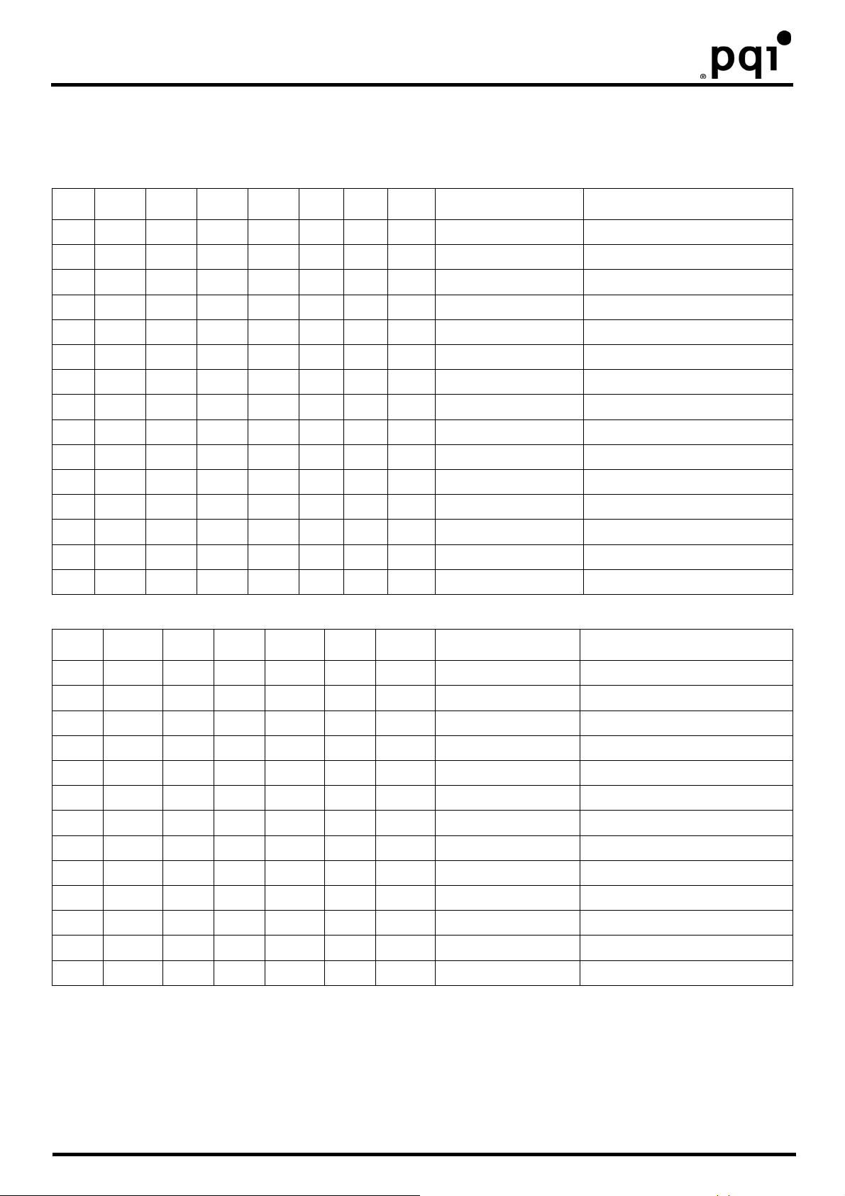
3. Interface Description
3.1 Card pin Assignment
Pin No.
Signal name I/O Signal name I/O Signal name I/O Signal name I/O
1
2
3
4
5
6
7
8
9
10
11
12
13
14
15
16
17
18
19
20
21
22
23
24
25
26
27
28
29
30
31
32
33
34
35
36
37
38
39
40
41
42
43
44
45
46
47
48
49
50
GND
D3 I/O D3 I/O D3 I/O D3 I/O
D4 I/O D4 I/O D4 I/O D4 I/O
D5 I/O D5 I/O D5 I/O D5 I/O
D6 I/O D6 I/O D6 I/O D6 I/O
D7 I/O D7 I/O D7 I/O D7 I/O
-CE1 I
A10 I
-OE I
A9
A8 I
A7
VCC
A6 I
A5 I
A4 I
A3 I
A2 I
A1 I
A0 I
D0 I/O D0 I/O D0 I/O D0 I/O
D1 I/O D1 I/O D1 I/O D1 I/O
D2 I/O D2 I/O D2 I/O D2 I/O
WP O -IOIS16 O -IOIS16 O -IOIS16 O
-CD2 O -CD2 O -CD2 O -CD2 O
-CD1 O -CD1 O -CD1 O -CD1 O
D11 I/O D11 I/O D11 I/O D11 I/O
D12 I/O D12 I/O D12 I/O D12 I/O
D13 I/O D13 I/O D13 I/O D13 I/O
D14 I/O D14 I/O D14 I/O D14 I/O
D15 I/O D15 I/O D15 I/O D15 I/O
-CE2 I -CE2 I -CS1 I -CS1 I
-VS1 O -VS1 O -VS1 O -VS1 O
-IORD I
-IOWR I
-WE I
RDY/-BSY O -IREQ O INTRQ O INTRQ O
VCC
-CSEL I -CSEL I -CSEL I -CSEL I
-VS2 O -VS2 O -VS2 O -VS2 O
RESET I RESET I -RESET I -RESET I
-WAIT O -WAIT O IORDY O IORDY O
-INPACK O -INPACK O RFU O DMARQ O
-REG I -REG I RFU I -DMACK I
BVD2 I/O -SPKR I/O -DASP I/O -DASP I/O
BVD1 I/O -STSCHG I/O -PDIAG I/O -PDIAG I/O
D8 I/O D8 I/O D8 I/O D8 I/O
D9 I/O D9 I/O D9 I/O D9 I/O
D10 I/O D10 I/O D10 I/O D10 I/O
GND
True IDE mode Memory card mode I/O card mode
PIO mode Multi-word DMA mode
-
GND
-
GND
-
GND
-CE1 I -CS0 I -CS0 I
A10 I A10 I A10 I
-OE I -ATASEL I -ATASEL I
I
A9
I
A9
I
A9
A8 I A8 I A8 I
I
-
A7
VCC
I
-
A7
VCC
I
-
A7
VCC
A6 I A6 I A6 I
A5 I A5 I A5 I
A4 I A4 I A4 I
A3 I A3 I A3 I
A2 I A2 I A2 I
A1 I A1 I A1 I
A0 I A0 I A0 I
-IORD I -IORD I -IORD I
-IOWR I -IOWR I -IOWR I
-WE I -WE I -WE I
-
-
VCC
GND
-
-
VCC
GND
-
-
VCC
GND
-
I
I
-
-
-
Rev. A.1 2/50 July. 2010
Page 7

CompactFlash Card
3.2 Card pin Description
Signal Name Dir Pin No. Description
A10 to A0
(PC Card Memory Mode)
A10 to A0
(PC Card I/O Mode)
A2 to A0
(True IDE Mode)
BVD1
(PC Card Memory Mode)
-STSCHG
(PC Card Memory Mode)
-PDIAG
(True IDE Mode)
BVD2
(PC Card Memory Mode)
-SPKR
(PC Card / I/O Mode)
-DASP
(True IDE Mode)
-CD1,-CD2
(PC Card Memory Mode)
-CE1,-CE2
(PC Card I/O Mode)
-CE1,-CE2
(PC Card I/O Mode)
-CS0,-CS1
(True IDE Mode)
-CSEL
(PC Card Memory Mode
-CSEL
(PC Card I/O Mode)
-CSEL
(True IDE Mode)
8,10,11,12,14,15,16,17,18,19,20
I
18,19,20
I/O 46
I/O 45
O 26,25
I 7,32
I 39
These address lines along with the-REG signal are
used to select the following: The I/O port address
registers within the CompactFlash Storage Card or
CF + Card, the memory mapped port add address
registers within the CompactFlash Storage Card or
CF+ Card , a byte in the card’s information structure
and its configuration control and status registers.
In True IDE Mode only A {2:0} are used to select the
one of eight registers in the Task File. The
remaining address lines should be grounded by the
host.
This signal is asserted high as BVD1 is not
supported
This signal is asserted low to alert the host to
changes in the RDY/-BSY and Write Protect states;
while the I/O interface is configured. Its use is
controlled by the Card Configured and Status
Register.
In the True IDE Mode, this input/output is the Pass
Diagnostic signal in the Master/Slave handshake
protocol.
This signal is asserted high, as BVD2 is not
supported.
This line is the Binary AUDIO OUTPUT FROM THE
CARD .if the Card does not support the Binary
Audio function, this line should be held negated.
In the True IDE Mode, this input/output is the Disk
Active/Slave Present signal in the Master/Slave
These Card Detect pins are connected to ground on
the CompcatFlash Storage Card or CF + Card.
They are used by the host to determine that the
CompactFlash Storage Card or CF +Card is fully
inserted into its socket.
These input signals are used both to select the card
and to indicate to the card whether a byte or a word
operation is being performed. –CE2 always
accesses the odd byte of the word depending on A0
and –CE2. A multiplexing scheme based on
A1.-CE1,-CE2 allows 8 bit hosts to access all data
on D0 to D7.
See Access specification below.
In the True IDE Mode CS0 is the chip select for the
task file registers while CS1 is used to select the
Alternate Status Register and the Device Control
Register.
This signal is not used for this mode.
This internally pulled up signal is used to configure
this device as a Master or a Slave when configured
in the True IDE Mode. When this pin is grounded,
this device is configured as a Master. When the
pins is open, this device is configured as a Slave.
Rev. A.1 3/50 July. 2010
Page 8

CompactFlash Card
Signal Name Dir Pin No. Description
D15 to D00
(PC Card Memory Mode)
D15 to D00
(PC Card I/O Mode)
D15 to D00
(True IDE Mode)
GND
(PC Card Memory Mode)
GND
(PC Card I/O Mode)
GND
(True IDE Mode)
-INPCAK
(PC Card Memory Mode)
-INPACK
(PC Card I/O Mode)
Reserved
(True IDE Mode
for PIO)
DMARQ
(True IDE Mode for
Multi-word DMA)
31,30,29,28,27,49,48,47,6,5,4,3,2,23,
I/O
22,21
─ 1,50
O 43
These lines carry the Data, Commands and Status
information between the host and the controller.D00
is the LSB of the Even Byte of the Word.D08 is the
LSB of the Even Byte of the Word.D08 is the LSB of
the Odd Byte of the Word.
True IDE Mode, all Task File operations occur in
byte mode on the low order bus D00 to D07 while
all data transfers are 16 bit using D00 to D15.
Ground
This signal is not used in this mode.
The Input Acknowledge signal is asserted by the
CompactFlash Storage Card or CF +Card when the
card is selected and responding to an I/O read
cycle at the address that is on the address bus. This
signal is used by the host to control the enable of
any input data buffers between the CompactFlash
Storage Card or CF +Card and the CPU.
In True IDE Mode this output signal is not used and
should not be connected at the host.
This signal is a DMA Request that is used for DMA
data transfers between host and device. It shall be
asserted by the device when it is ready to transfer
data to or from the host. For Multiword DMA
transfers, the direction of data transfer is controlled
by –IORD and –IOWR. This signal is used in a
handshake manner with –DMACK, i.e., the device
shall wait until the host asserts –DMACK before
negating DMARQ, and reasserting DMARQ if there
is more data to transfer.
DMARQ shall not be driven when the device is not
selected.
While a DMA operation is in progress, -CS0 and
–CS1 shall be held negated and the width of the
transfers shall not be 16 bits.
If there is no hardware support for DMA mode in the
host, this output signal is not used and should not
be connected at the host. In this case, the BIOS
must report that DMA mode is not supported by the
host so that device drivers will not attempt DMA
mode.
A host that does not support DMA mode and
implements both PCMCIA mode and True-IDE
modes of operation need not alter the PCMCIA
mode connections while in True-IDE mode as long
as this does not prevent proper operation in any
mode.
Rev. A.1 4/50 July. 2010
Page 9

CompactFlash Card
Signal Name Dir Pin No. Description
-IORD
(PC Card Memory Mode)
-IORD
(PC Card I/O Mode)
-IORD
(True IDE Mode)
-IOWR
(PC Card Memory Mode)
-IOWR
(PC Card I/O Mode)
-IOWR
(True IDE Mode)
-OE
(PC Card Memory Mode)
-OE
(PC Card I/O Mode)
-ATA SEL
(True IDE Mode)
RDY/BSY
(PC Card Memory Mode)
-IREQ
(PC Card I/O Mode)
INTRQ
(True IDE Mode)
I 34
I 35
I 9
O 37
This signal is not used in this mode.
This is an I/O Read strobe generated by the host.
This signal gates I/O data onto the bus from the
CompactFlash Storage Card or CF +Card when the
card is configured to use the I/O interface.
In True IDE Mode, this signal has same function as
in PC Card I/O Mode.
This signal is not used in this mode.
The I/O Write strobe pulse is used to clock I/O data
on the Card Data bus into the CompcatFlash
Storage Card or CF +Card controller registers when
the CompactFlash Storage Card or CF +Card is
configured to use the I/O interface. The clocking will
occur on the negative to positive edge of the signal
(Trailing edge)
In True IDE Mode, this signal has the same function
as in PC Card I/O Mode.
This is an Output Enable strobe generated by the
host interface. It is used to read data from the
CompactFlash Storage Card or CF +Card in
Memory Mode and to read the CIS and
configuration registers.
In PC Card I/O Mode. This signal is used to read
the CIS and configuration registers.
To enable True IDE Mode this input should be
grounded by the host.
In Memory Mode this signal is set high when the
CompactFlash Storage Card or CF +Card is ready
to accept a new data transfer operation and held
low when the card is busy . The Host memory card
socket must provide a pull-up resistor. At power up
and at Reset the RDY/-BSY signal is held low
(busy) until the CompactFlash Storage Card or CF
+Card has completed its power up or reset function.
No access of any type should be made to the
CompactFlash Storage Card or CF +Card during
this time. The RDY/-BSY signal is held high
(disabled from being busy) whenever the following
condition is true. The CompactFlash Storage Card
or CF +Card has been powered up with + RESET
continuously disconnected or asserted.
Operation-After the CompactFlash Storage Card or
CF + Card has been configured for I/O operation;
this signal is used as interrupt Request. This line is
strobe low to generate a pulse mode interrupt or
held low for a level mode interrupt.
In True IDE Mode signal is the active high interrupt
Request to the host.
Rev. A.1 5/50 July. 2010
Page 10

CompactFlash Card
Signal Name Dir Pin No. Description
This signal is used during Memory Cycles to
-REG
(PC Card Memory Mode)
-REG
(PC Card I/O Mode)
Reserved
(True IDE Mode
for PIO)
-DMACK
(True IDE Mode for
Multi-word DMA)
RESET
(PC Card Memory Mode)
RESET
(PC Card I/O Mode)
-RESET
(True IDE Mode)
VCC
(PC Card Memory Mode)
(PC Card I/O Mode)
(True IDE Mode)
-VS1 /-VS2
(PC Card Memory Mode)
(PC Card I/O Mode)
(True IDE Mode)
-WAIT
(PC Card Memory Mode)
-WAIT
(PC Card I/O Mode)
IORDY
(True IDE Mode)
I 44
I 41
─ 13,38
O 33,40
O 42
distinguish between Common Memory and
Register(Attribute) Memory accesses. High for
Common Memory. Low for Attribute Memory.
The signal must also be active (low) during I/O
Cycles when the I/O address is on the Bus.
In the True IDE Mode, this input signal is not used
and should be driven high or connected to VCC by
the host.
This is a DMA acknowledge signal that is asserted
by the host in response to DMARQ to initiate DMA
transfers.
While DMA operations are not active, the card shall
ignore the –DMACK signal, including a floating
condition.
If DMA operation is not supported by a True-IDE
mode only host, this signal should be driven high or
connected to VCC by the host.
A host that does not support DMA mode and
implements both PCMCIA and True-IDE modes of
operation need not alter the PCMCIA mode
connections while in True-IDE mode as long as this
does not prevent proper operation all modes.
The CompactFlash Storage Card or CF+ Card is
Reset when the RESET pin is high with the following
important exception:
The host may leave the RESET pin open or keep it
continually high from the application of power
without causing a continuous Reset of the card.
Under either of these conditions, the card shall
emerge from power-up having completed an initial
Reset.
The CompactFlash Storage Card or CF +Card is
also Reset when the Soft Reset bit in the Card
Configuration Option Register is set.
This signal is the same as the PC Card Memory
Mode signal.
In the True IDE Mode this input pin is the active low
hardware reset form the host.
+5V +3.3V power.
Voltage Sense Signals. –VS1 is grounded so that the
CompactFlash Storage Card or CF + Card CIS can
be read at 3.3 volts and –VS2 is reserved by
PCMCIA for a secondary voltage.
The –WAIT signal is driven low by the CompactFlash
Storage Card or CF +Card to signal the host to delay
completion of a memory or I/O cycle that is in
progress.
In True IDE Mode this output signal may be used as
IORDY.
Rev. A.1 6/50 July. 2010
Page 11

CompactFlash Card
Signal Name Dir Pin No. Description
This is a signal driven by the host and used for
-WE
(PC Card Memory Mode)
-WE
(PC Card I/O Mode)
-WE
(True IDE Mode)
WP
(PC Card Memory Mode)
-IOIS16
(PC Card I/O Mode)
-IOIS16
(True IDE Mode)
I 36
O 24
starting memory write data to the registers of the
CompactFlash Storage Card or CF + Card when the
card is configured I the memory interface mode. It is
also used for writing the configuration registers.
In PC Card I/O Mode, this signal is used for writing
the configuration registers.
In True IDE Mode this input signal is not used and
should be connected to VCC by the host.
Memory Mode-The CompactFlash Storage Card or
CF + Card does not have a write protect switch. This
signal is held low after the completion of the reset
initialization sequence.
I/O Operation-When the CompactFlash Storage
Card or CF + Card is configured for I/O Operation
Pin 24 is used for the –I/O Selected is 16 Bit Port
(-IOIS16) function. A Low signal indicates that a 16
bit or odd byte only operation can be performed at
the addressed port.
In True IDE Mode this output signal is asserted low
when this device is expecting a word data transfer
cycle.
Rev. A.1 7/50 July. 2010
Page 12
CompactFlash Card
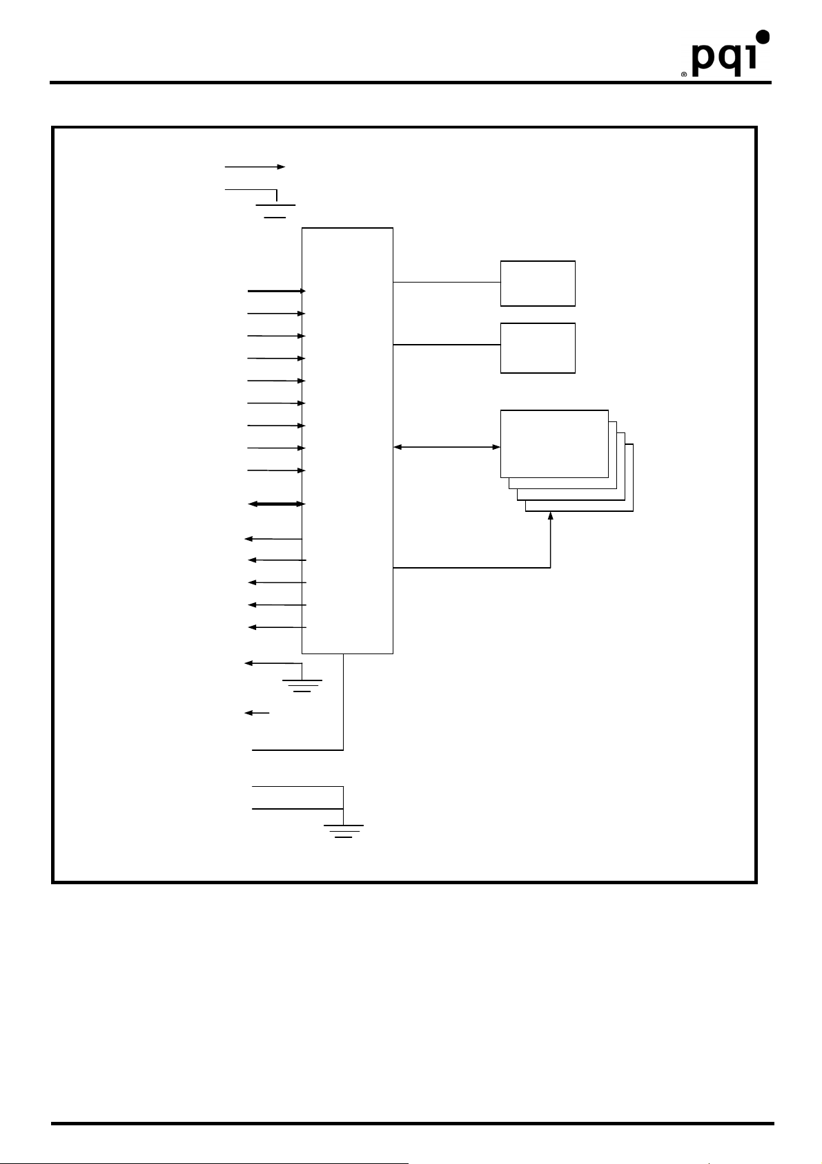
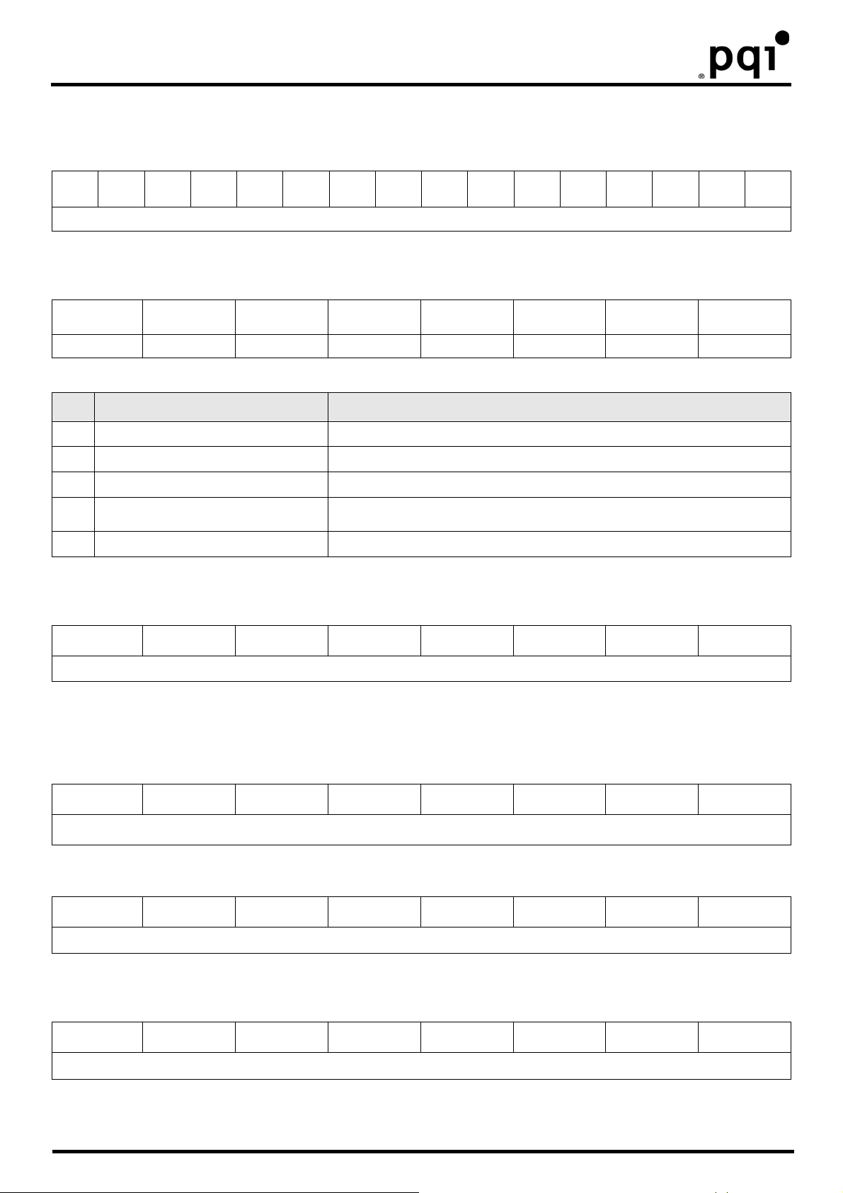
3.3 Card Block Diagram
VCC
GND
Internal VCC
A0 to A10
-CE1,-CE2
-OE,-ATASEL
-WE
-IORD
-IOWR
-REG
RESET/-RESET
-CSEL
D0 to D15
RDY/-BSY/-IREQ/INTRQ
WP/-IOIS16
-INPACK
BVD1/-STSCHG/-PDIA
-WAIT/IORDY
VS1
VS1
Controller
Flash memory
bus
Reset IC
Clock
NAND FLASH
Control signal
VS2
OPEN
BVD2/-SPKR/-DAS
-CD1
-CD2
●
Rev. A.1 8/50 July. 2010
Page 13
CompactFlash Card
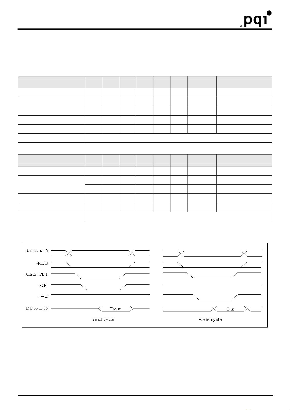
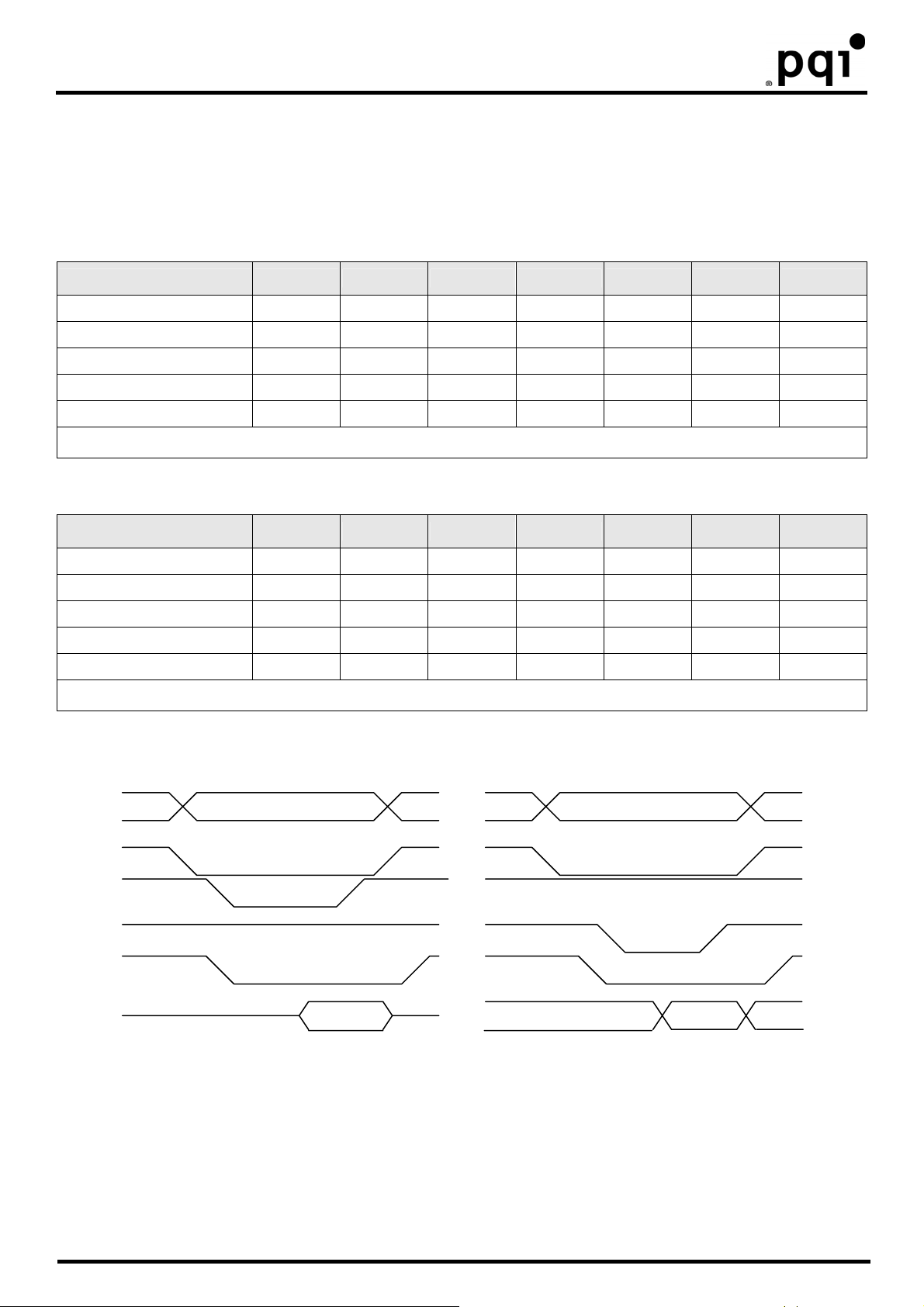
4. Access specification
4.1 Attribute access specifications
When CIS-ROM region or Configuration register region is accessed, read and write operations are executed under the
condition of –REG = “L” as follows. That region can be accessed by Byte/Word/Odd-byte modes, which are defined by PC
card standard specifications.
Attribute Read Access Mode
Mode -REG -CE2 -CE1 A0 -OE -WE D8 to D15 D0 to D7
Standby mode X H H X X X High-Z High-Z
Byte access (8-it)
Word access (16-it) L L L X L H invalid even byte
Odd byte access (8bit) L L H X L H invalid High-Z
Note: X → L or H
L H L L L H High-Z even byte
L H L H L H High-Z invalid
Attribute Write Access Mode
Mode -REG -CE2 -CE1 A0 -OE -WE D8 to D15 D0 to D7
Standby mode × H H × × × Don’t care Don’t care
Byte access (8bit)
Word access (16bit) L L L × H L Don’t care even byte
Odd byte access (8bit) L L H × H L Don’t care Don’t care
Note: X → L or H
L H L L H L Don’t care even byte
L H L H H L Don’t care Don’t care
Attribute Access Timing Example
Rev. A.1 9/50 July. 2010
Page 14

CompactFlash Card
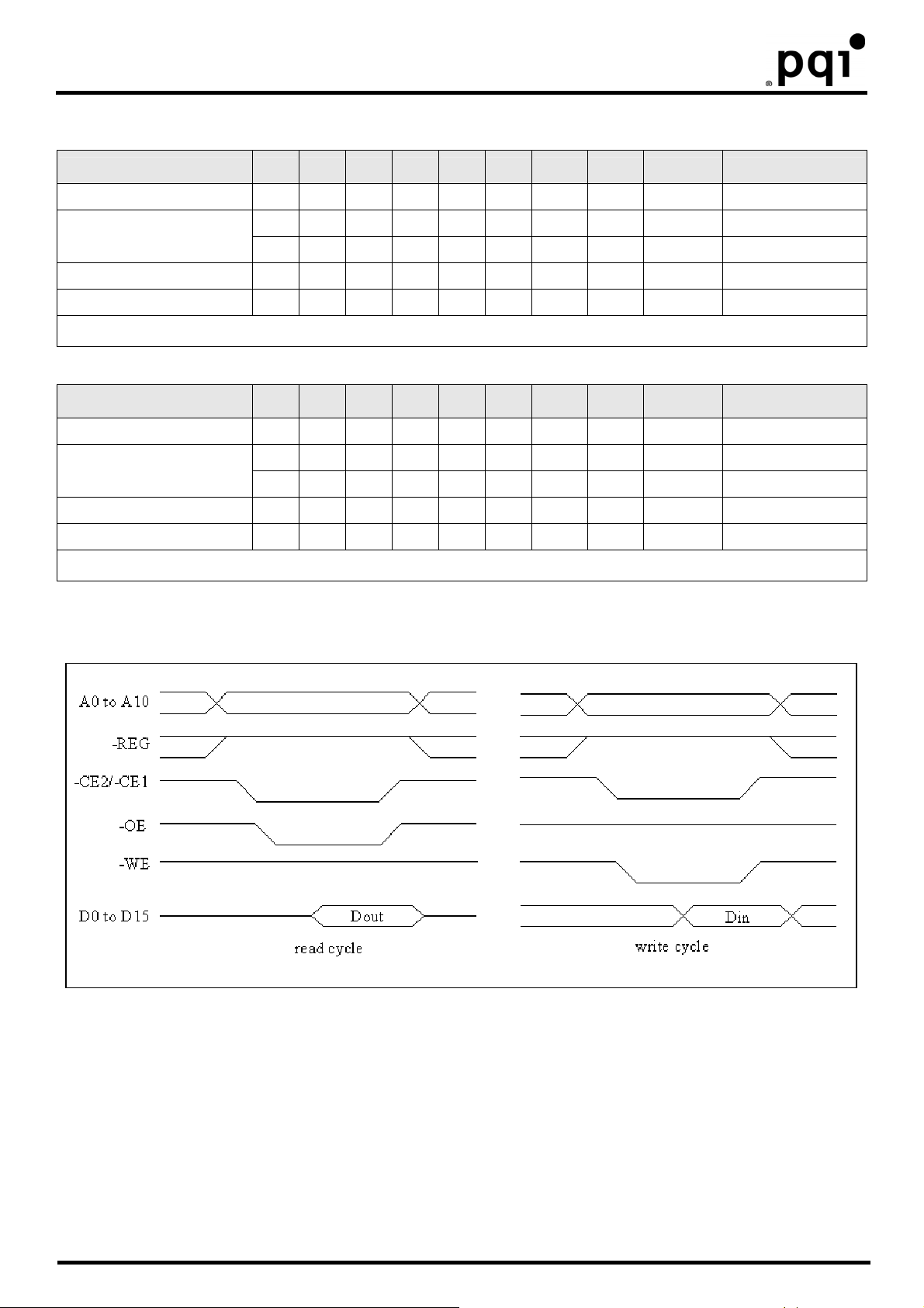
4.2 Task file Register access specifications
There are two cases of Task File register mapping, one is mapped I/O address area, the other is mapped Memory
address area. Each case of Task File registers read and write operations is executed under the condition as follows.
That area can be accessed by Byte/World/Odd Byte modes, which are defined by PC card standard specifications.
4.2.1 I/O address map
Task File Register Read Access Mode (1)
Mode -REG -CE2 -CE1 A0 -IORD -IOWR -OE -WE D8 to D15 D0 to D7
Standby mode X H H X X X X X High-Z High-Z
Byte access (8bit)
Word access (16bit) L L L X L H H H odd byte even byte
Odd byte access (8bit) L L H X L H H H odd byte High-Z
Note: X→ L or H
L H L L L H H H High-Z even byte
L H L H L H H H High-Z odd byte
Task File Register Write Access Mode (1)
Mode -REG -CE2 -CE1 A0 -IORD -IOWR -OE -WE D8 to D15 D0 to D7
Standby mode × H H × × × × × Don’t care Don’t care
Byte access(8-bit)
Word access(16-bit) L L L × H L H H odd byte even byte
Odd byte access(8-bit) L L H × H L H H odd byte don’t care
Note: X→ L or H
L H L L H L H H Don’t care even byte
L H L H H L H H Don’t care odd byte
Task File Register Access Timing Example (1)
Rev. A.1 10/50 July. 2010
Page 15
CompactFlash Card
4.2.2 Memory address map
Task File Register Read Access Mode (2)
Mode -REG -CE2 -CE1 A0 -OE -WE -IORD -IOWR D8 to D15 D0 to D7
Standby mode X H H X X X X X High-Z High-Z
Byte access (8bit)
Word access (16bit) H L L X L H H H odd byte even byte
Odd byte access (8bit) H L H X L H H H odd byte High-Z
Note: X→ L or H
Task File Register Write Access Mode (2)
Mode -REG -CE2 -CE1 A0 -OE -WE -IORD -IOWR D8 to D15 D0 to D7
Standby mode X H H X X X X X Don’t care Don’t care
H H L L L H H H High-Z even byte
H H L H L H H H High-Z odd byte
Byte access (8bit)
Word access (16bit) H L L X H L H H odd byte even byte
Odd byte access (8bit) H L H X H L H H odd byte don’t care
Note: X→ L or H
H H L L H L H H Don’t care even byte
H H L H H L H H Don’t care odd byte
Task File Register Access Timing Example (2)
Rev. A.1 11/50 July. 2010
Page 16
CompactFlash Card
4.2.3 True IDE Mode
The card can be configured in a True IDE This card is configured in this mode only when the –OE input signal is
asserted GND by the host. In this True IDE mode Attribute Registers are not accessible from the host. Only I/O
operation to the task file and data register is allowed. If this card is configured during power on sequence, data register
is accessed in word (16-bit). The card permits 8-bit accessed if the user issues a Set Feature Command to put the
device in 8-bit mode.
True IDE Mode Read I/O Function
Mode -CE2 -CE1 A0~A2 -IORD -IOWR D8 to D15 D0 to D7
Invalid mode L L X X X High-Z High-Z
Standby mode H H X X X High-Z High-Z
Data register access H L 0 L H Odd byte even byte
Alternate status access L H 6H L H High-Z Status out
Other task file access H L 1~7H L H High-Z Data
Note: X→ L or H
True IDE Mode Write I/O Function
Mode -CE2 -CE1 A0~A2 -IORD -IOWR D8 to D15 D0 to D7
Invalid mode L L X X X Don’t card Don’t card
Standby mode H H X X X Don’t card even byte
Data register access H L 0 H L Odd byte Don’t card
Alternate status access L H 6H H L Don’t card Control in
Other task file access H L 1~7H H L Odd byte Data
Note: X→ L or H
True IDE Mode I/O Access Timing Example
A0~A2
-CE
-IORD
-IORW
-IOS16
D0~D15
Din
Dout
Rev. A.1 12/50 July. 2010
Page 17
CompactFlash Card
4.3 Configuration register specification
This card supports four Configuration registers for the purpose of the configuration and observation of this card.
4.3.1 Configuration Option register (Address 200H)
This register is used for the configuration of the card configuration status and for the issuing soft reset to the card.
bit7 bit6 bit5 bit4 bit3 bit2 bit1 bit0
SRESET LevIREQ INDEX
Note: initial value: 00H
Name R/W Function
Setting this bit to “1”, places the card in the reset state (Card Hard Reset). This operation is equal
SRESET
(HOST->)
R/W
to Hard Reset, except this bit is not cleared. Then this bit set to “0”,places the card in the reset
state of Hard Reset (This bit is set to “0” by Hard Reset). Card configuration status is reset and the
card internal initialized operation starts when Card Hard Reset is executed, so next access to the
card should be the same sequence as the power on sequence.
LevIREQ
(HOST->)
INDEX
(HOST->)
Note: initial value → 00H
R/W
R/W
This bit sets to “0” when pulse mode interrupt is selected and “1 when level mode interrupt is
selected.
This bits is used for select operation mode of the card as follows.
When Power on, Card Hard Reset and Soft Reset, this data is “000000” for the purpose of Memory
card interface recognition.
INDEX bit assignment
INDEX bit
5 4 3 2 1 0 Card mode Task File register address Mapping mode
0 0 0 0 0 0 Memory card 0H to FH, 400H to 7FFH memory mapped
0 0 0 0 0 1 I/O card ××0H to ××FH Contiguous I/O mapped
0 0 0 0 1 0 I/O card 1F0H to 1F7H, 3F6H to 3F7H Primary I/O mapped
0 0 0 0 1 1 I/O card 170H to 177H, 376H to 377H Secondary I/O mapped
4.3.2 Configuration and Status register (Address 202H)
This register is used for observing the card state.
bit7 bit6 bit5 bit4 bit3 bit2 bit1 bit0
CHGED SIGCHG IOIS8 0 0 PWD INTR 0
Note: initial value: 00H
Rev. A.1 13/50 July. 2010
Page 18

CompactFlash Card
Name R/W Function
CHGED
(CARD->)
SIGCHG
(HOST->)
IOIS8
(HOST->)
PWD
(HOST->)
INTR
(CARD->)
R
R/W
R/W The host sets this field to “1” when it can provide I/O cycles only with on 8bit data bus (D7 to D0).
R/W
R
This bit indicates that CRDY-BSY bit on Pin Replacement register is set to “1”. When CHGED bit is
set to “1”, -STSCHG pin is held “L” at the confition of SIGCHG bit set to “1” and the card configured
for the I/O interface.
This bit is set or reset by the host for enabling and disabling the status-change signal (-STSCHG
pin). When the card is configured I/O card interface and this bit is set to “1”, -STSCHG pin is
controlled by CHGED bit. If this bit is set to “0”, -STSCHG pin is kept “H”.
When this bit is set to “1”, the card enters sleep state (Power Down mode). When this bit is reset to
“0”, the card transfers to idle state (active mode). RRDY/-BSY bit on Pin Replacement Register
becomes BUSY when this bit is changed. RRDY/-BSY will not become Ready until the power state
requested has been entered. This card automatically powers down when it is idle, and powers
back up when it receives a command.
This bit indicates the internal state of the interrupt request. This bit state is available whether I/O
card interface has been configured or not. This signal remains true until the condition which cased
the interrupt request has been serviced. If interrupts are disabled by the –IEN bit in the
Device Control Register, this bit is a zero.
4.3.3 Pin Replacement register (Address 204H)
This register is used for providing the signal state of –IREQ signal when the card configured I/O card interface.
bit7 bit6 bit5 bit4 bit3 bit2 bit1 bit0
0 0 CRDY/-BSY 0 1 1 RRDY/-BSY 0
Note: initial value: 00H
Name R/W Function
CRDY/-BSY
(HOST->)
RRDY/-BSY
(HOST->)
R/W
R/W
This bit is set to “1” when the RRDY/-BSY bit changes state. This bit may also be written by the
host.
When read, this bit indicates +READY pin states. When written, this bit is used for CRDY/-Bsy bit
masking.
4.3.4 Socket and Copy register (Address 206H)
This register is used for identification of the card from the other card. Host can read and write this register. This
register should be set by host before this card’s Configuration Option register set.
bit7 bit6 bit5 bit4 bit3 bit2 bit1 bit0
0 0 0 DRV# 0 0 0 0
Note: initial value: 00H
Name R/W Function
DRV#
(HOST->)
R/W
These fields are used for the configuration of the plural cards. When host configures the plural
cards, written the card’s copy number in this field. In this way, host can perform the card’s
master/slave organization.
Rev. A.1 14/50 July. 2010
Page 19
CompactFlash Card
4.4 CIS Information
CIS information of Compact Flash Card is defined as follows.
Address Data 7 6 5 4 3 2 1 0 Description of Contents CIS function
000H 01H CISTPL_DEVICE Device Info tuple Tuple code
002H 03H TPL_LINK Link length is 3 byte Link to next tuple
Type=D: I/O device
004H D9H Device Type W Speed
006H 01H # address units –1 unit size 2 Kbytes of address space Device size
008H FFH CISTPL_END End of CISTPL_DEVICE End marker
00AH 1Ch CISTPL_DEVICE_OC
00CH 04H TPL_LINK Link length is 4 byte Link to next tuple
00EH 02H Ext Reserved 3V M
010H D9H Device Type W Speed
012H 01H # address units –1 unit size 2 Kbytes of address space Device size
014H FFH CISTPL_END End of CISTPL_DEVICE_OC End marker
016H 18H CISTPL_JEDEC_C JEDEC programming info tuple Tuple code
018H 02H TPL_LINK Link length is 2 byte Link to next tuple
01AH DFH JEDEC ID Device manufacturer ID Manufacturer ID
01CH 01H JEDEC Info Manufacturer specific info Manufacturer info
01EH 20H CISTPL_MANFID Manufacturer ID tuple Tuple code
020H 04H TPL_LINK Link length is 4 bytes Link to next tuple
022H 00H
024H 00H
026H 00H
028H 00H
02AH 21H CISTPL_FUNCID Function ID tuple Tuple code
02CH 02H CISTPL_LINK Link length is 2 bytes Link to next tuple
02EH 04H TPLFID_FUNCTION Fixed disk drive Function code
030H 01H Reserved R P
032H 22H CISTPL_FUNCE Function Extension tuple Tuple code
034H 02H CISTPL_LINK Link length is 2 bytes Link to next tuple
036H 01H Disk function extension tuple Disk interface information TPLFE_TYPE
038H 01H Disk interface type PC card ATA interface TPLFE_DATA
03AH 22H CISTPL_FUNCE Function Extension tuple Tuple code
03CH 03H CISTPL_LINK Link length is 3 bytes Link to next tuple
TPLMID_MANF PC Card manufacturer code Manufacturer ID
TPLMID_CARD Manufacturer specific info Manufacturer info
WPS=1: no WP switch
Speed=1: 250 ns
Common memory other
operating conditions tuple
3V=1: dual voltage card,
conditions for 3.3V operation
M=0: conditions without wait
Type=D: I/O device
WPS=1: no WP switch
Speed=1: 250 ns
R=0: no expansion ROM
P=1: configure at POST
Device type, WPS, speed
Tuple code
Other Conditions
Information
Device type, WPS, speed
System init byte
TPLFID_SYSINIT
Rev. A.1 15/50 July. 2010
Page 20

CompactFlash Card
Address Data 7 6 5 4 3 2 1 0 Description of Contents CIS function
03EH 02H Disk function extension tuple PC card ATA basic features TPLFE_TYPE
040H 04H Reserved D U S V
042H 07H R I E N P
044H 1AH CISTPL_CONFIG Configuration Tuple Tuple code
046H 05H TPL_LINK Link length is 5 bytes Link to next tuple
048H 01H RFS RMS RAS
04AH 07H TPCC_LAST Last configuration entry is 07H Last entry index
04CH 00H TPCC_RADR (LSB)
04EH 02H TPCC_RADR (MSB)
050H 0FH TPCC_RMSK
052H 1BH CISTPL_CFTABLE_ENTRY Configuration tuple Tuple code
054H 0BH CISTPL_LINK Link length is 11 bytes Link to next tuple
056H C0H I D Configuration Index
058H C0H W R P B Interface type
05AH A1H M MS IR IO T Power
05CH 27H R DI PI AI SI HV LV NV
05EH 55H X Mantissa Exponent Nominal voltage 5.0V
060H 4DH X Mantissa Exponent Minimum voltage 4.5V
062H 5DH X Mantissa Exponent Maximum voltage 5.5V
064H 75H X Mantissa Exponent Peak current 80 mA
D=0: single drive on card
U=0: no unique serial number
S=1: silicon device
V=0: no V
I=0: twin IOIS16# unspecified
E=0: index bit not emulated
N=0: I/O includes 0x3F7
P=7: sleep, standby, idle
supported
RFS: reserved
RMS: 1 byte register mask
RAS: 2 bytes base address
Configuration registers are
located at 0200H
Configuration registers 0 to 3
are present
Memory mapped configuration,
index=0
I=1: Interface byte follows
D=1: Default entry
W=1: wait required
R=1: ready/busy active
P=0: WP not used
B=0: BVD1, BVD2 not used
Type=0: Memory interface
M=1: misc info present
MS=1: 2 byte memory length
IR=0: no interrupt is used
IO=0: no I/O space is used
T=0: no timing info specified
Power=1: V
DI: no power-down current
PI=1: peak current info
AI: no average current info
SI: no static current info
HV=1: max voltage info
LV=1: min voltage info
NV=1: nominal voltage info
required
PP
info, no VPP
CC
TPLFE_TYPE
TPLFE_TYPE
Size of fields
TPCC_SZ
Configuration
register location
Configuration
reg-ister present
mask
Configuration Table
Index Byte
TPCE_INDX
Interface Description
TPCE_IF
Feature Selection
Byte TPCE_FS
Power Description
Structure Parameter
Selection Byte
TPCE_PD
Rev. A.1 16/50 July. 2010
Page 21

CompactFlash Card
Address Data 7 6 5 4 3 2 1 0 Description of Contents CIS function
066H 08H Length in 256 byte units (LSB)
068H 00H Length in 256 byte units (MSB)
06AH 21H X R P RO A T
06CH 1BH CISTPL_CFTABLE_ENTRY Configuration tuple Tuple code
06EH 06H CISTPL_LINK Link length is 6 bytes Link to next tuple
070H 00H I D Configuration Index
072H 01H M MS IR IO T Power Power=1: VCC info, no VPP TPCE_FS
D
074H 21H R
076H B5H X Mantissa Exponent X=1: extension byte present
078H 1EH X Extension Nominal voltage 3.30V
07AH 4DH X Mantissa Exponent Peak current 45 mA
07CH 1BH CISTPL_CFTABLE_ENTRY Configuration tuple Tuple code
07EH 0DH CISTPL_LINK Link length is 13 bytes Link to next tuple
080H C1H I D Configuration Index
082H 41H W R P B Interface type
084H 99H M MS IR IO T Power
086H 27H R DI PI AI SI HV LV NV
088H 55H X Mantissa Exponent Nominal voltage 5.0V
08AH 4DH X Mantissa Exponent Minimum voltage 4.5V
08CH 5DH X Mantissa Exponent Maximum voltage 5.5V
08EH 75H X Mantissa Exponent Peak current 80 mA
090H 64H R S E IO
PI AI SI HV LV NV
I
Length of memory space is 2
Kbytes
X=0: no more misc fields
P=1: power-down supported
RO=0:read/write media
A=0: audio not supported
T=1: max twins is 1
Memory mapped configuration,
index=0
PI=1: peak current info
NV=1: nominal voltage info
I/O mapped, index=1
I=1: Interface byte follows
D=1: Default entry
W=0: wait not required
R=1: ready/busy active
P=0: WP not used
B=0: BVD1, BVD2 not used
Type=1: I/O interface
M=1: misc info present
MS=0: no memory space info
IR=1: interrupt is used
IO=1: I/O space is used
T=0: no timing info specified
Power=1: V
DI: no power-down current
PI=1: peak current info
AI: no average current info
SI: no static current info
HV=1: max voltage info
LV=1: min voltage info
NV=1: nominal voltage info
S=1: support 16 bit hosts
E=1: support 8 bit hosts
IO=4: 4 address lines decoded
info, no VPP
CC
Memory space- descr.
TPCE_MS
Miscellaneous
features TPCE_MI
TPCE_INDX
TPCE_PD
TPCE_INDX
TPCE_IF
TPCE_FS
TPCE_PD
TPCE_IO
Rev. A.1 17/50 July. 2010
Page 22

CompactFlash Card
Address Data 7 6 5 4 3 2 1 0 Description of Contents CIS function
S=1: interrupt sharing logic
P=1: pulse mode supported
L=1: level mode supported
092H F0H S P L M V B I N
094H FFH IRQ7..0
096H FFH IRQ15..8
98H 21H X R P RO A T
09AH 1BH CISTPL_CFTABLE_ENTRY Configuration tuple Tuple code
09CH 06H CISTPL_LINK Link length is 6 bytes Link to next tuple
09EH 01H I D Configuration Index I/O mapped, index=1 TPCE_INDX
0A0H 01H M MS IR IO T Power Power=1: VCC info, no VPP TPCE_FS
0A2H 21H R DI PI AI SI HV LV NV
0A4H B5H X Mantissa Exponent X=1: extension byte present
0A6H 1EH X Extension Nominal voltage 3.30V
0A8H 4DH X Mantissa Exponent Peak current 45 mA
0AAH 1BH CISTPL_CFTABLE_ENTRY Configuration tuple Tuple code
0ACH 12H CISTPL_LINK Link length is 18 bytes Link to next tuple
0AEH C2H I D Configuration Index
0B0H 41H W R P B Interface type
0B2H 99H M MS IR IO T Power
0B4H 27H R DI PI AI SI HV LV NV
0B6H 55H X Mantissa Exponent Nominal voltage 5.0V
0B8H 4DH X Mantissa Exponent Minimum voltage 4.5V
0BAH 5DH X Mantissa Exponent Maximum voltage 5.5V
M=1: masks V..N present
V=0: no vendor unique IRQ
B=0: no bus error IRQ
I=0: no I/O check IRQ
N=0: no NMI
Interrupt signal may be
assigned to any host IRQ
X=0: no more misc fields
P=1: power-down supported
RO=0:read/write media
A=0: audio not supported
T=1: max twins is 1
PI=1: peak current info
NV=1: nominal voltage info
I/O mapped, index=2
I=1: Interface byte follows
D=1: Default entry
W=0: wait not required
R=1: ready/busy active
P=0: WP not used
B=0: BVD1, BVD2 not used
Type=1: I/O interface
M=1: misc info present
MS=0: no memory space info
IR=1: interrupt is used
IO=1: I/O space is used
T=0: no timing info specified
Power=1: V
DI: no power-down current
PI=1: peak current info
AI: no average current info
SI: no static current info
HV=1: max voltage info
LV=1: min voltage info
NV=1: nominal voltage info
info, no VPP
CC
TPCE_IR
TPCE_MI
TPCE_PD
TPCE_INDX
TPCE_IF
TPCE_FS
TPCE_PD
Rev. A.1 18/50 July. 2010
Page 23

CompactFlash Card
Address Data 7 6 5 4 3 2 1 0 Description of Contents CIS function
0BCH 75H X Mantissa Exponent Peak current 80 mA
R=1: range follows
0BEH EAH R S E IO
0C0H 61H LS AS NR
0C2H F0H Base address 1 (LSB)
0C4H 01H Base address 1 (MSB)
0C6H 07H Address range 1 length
0C8H F6H Base address 2 (LSB)
0CAH 03H Base address 2 (MSB)
0CCH 01H Address range 2 length
0CEH EEH S P L M IRQN
0D0H 21H X R P RO A T
0D2H 1BH CISTPL_CFTABLE_ENTRY Configuration tuple Tuple code
0D4H 06H CISTPL_LINK Link length is 6 bytes Link to next tuple
0D6H 02H I D Configuration Index I/O mapped, index=2 TPCE_INDX
0D8H 01H M MS IR IO T Power Power=1: VCC info, no VPP TPCE_FS
0DAH 21H R DI PI AI SI HV LV
0DCH B5H X Mantissa Exponent X=1: extension byte present
0DEH 1EH X Extension Nominal voltage 3.30V
0E0H 4DH X Mantissa Exponent Peak current 45 mA
0E2H 1BH CISTPL_CFTABLE_ENTRY Configuration tuple Tuple code
0E4H 12H CISTPL_LINK Link length is 18 bytes Link to next tuple
0E6H C3H I D Configuration Index
0E8H 41H W R P B Interface type
0EAH 99H M MS IR IO T Power
S=1: support 16 bit hosts
E=1: support 8 bit hosts
IO=10: 10 lines decoded
LS=1: 1 byte length
AS=2: 2 byte address
NR=1: 2 address ranges
Address range 1
0x1F0 to 0x1F7
Address range 2
0x3F6 to 0x3F7
S=1: interrupt sharing logic
P=1: pulse mode supported
L=1: level mode supported
M=0: masks V.N not present
IRQN=14: use interrupt 14
X=0: no more misc fields
P=1: power-down supported
RO=0:read/write media
A=0: audio not supported
T=1: max twins is 1
NVPI=1: peak current info
NV=1: nominal voltage info
I/O mapped, index=3
I=1: Interface byte follows
D=1: Default entry
W=0: wait not required
R=1: ready/busy active
P=0: WP not used
B=0: BVD1, BVD2 not used
Type=1: I/O interface
M=1: misc info present
MS=0: no memory space info
IR=1: interrupt is used
IO=1: I/O space is used
T=0: no timing info specified
Power=1: V
info, no VPP
CC
TPCE_IO
TPCE_IR
TPCE_MI
TPCE_PD
TPCE_INDX
TPCE_IF
TPCE_FS
Rev. A.1 19/50 July. 2010
Page 24

CompactFlash Card
Address Data 7 6 5 4 3 2 1 0 Description of Contents CIS function
DI: no power-down current
PI=1: peak current info
AI: no average current info
0ECH 27H R DI PI AI SI HV LV NV
0EEH 55H X Mantissa Exponent Nominal voltage 5.0V
0F0H 4DH X Mantissa Exponent Minimum voltage 4.5V
0F2H 5DH X Mantissa Exponent Maximum voltage 5.5V
0F4H 75H X Mantissa Exponent Peak current 80 mA
0F6H EAH R S E IO
0F8H 61H LS AS NR
0FAH 70H Base address 1 (LSB)
0FCH 01H Base address 1 (MSB)
0FEH 07H Address range 1 length
100H 76H Base address 2 (LSB)
102H 03H Base address 2 (MSB)
104H 01H Address range 2 length
106H EEH S P L M IRQN
108H 21H X R P RO A T
10AH 1BH CISTPL_CFTABLE_ENTRY Configuration tuple Tuple code
10CH 06H CISTPL_LINK Link length is 6 bytes Link to next tuple
10EH 03H I D Configuration Index I/O mapped, index=3 TPCE_INDX
110H 01H M MS IR IO T Power Power=1: VCC info, no VPP TPCE_FS
112H 21H R DI PI AI SI HV LV NV
114H B5H X Mantissa Exponent X=1: extension byte present
116H 1EH X Extension Nominal voltage 3.30V
118H 4DH X Mantissa Exponent Peak current 45 mA
11AH 1BH CISTPL_CFTABLE_ENTRY Configuration tuple Tuple code
11CH 04H CISTPL_LINK Link length is 4 bytes Link to next tuple
11EH 07H I D Configuration Index I/O mapped, index=7 TPCE_INDX
120H 00H M MS IR IO T Power No feature descriptions follow TPCE_FS
SI: no static current info
HV=1: max voltage info
LV=1: min voltage info
NV=1: nominal voltage info
R=1: range follows
S=1: support 16 bit hosts
E=1: support 8 bit hosts
IO=10: 10 lines decoded
LS=1: 1 byte length
AS=2: 2 byte address
NR=1: 2 address ranges
Address range 1
0x170 to 0x177
Address range 2
0x376 to 0x377
S=1: interrupt sharing logic
P=1: pulse mode supported
L=1: level mode supported
M=0: masks V..N not present
IRQN=14: use interrupt 14
X=0: no more misc fields
P=1: power-down supported
RO=0:read/write media
A=0: audio not supported
T=1: max twins is 1
PI=1: peak current info
NV=1: nominal voltage info
TPCE_PD
TPCE_IO
TPCE_IR
TPCE_MI
TPCE_PD
Rev. A.1 20/50 July. 2010
Page 25
CompactFlash Card
Address Data 7 6 5 4 3 2 1 0 Description of Contents CIS function
122H 28H Hyper stone specific data
124H D3H Hyper stone specific data
126H 14H CISTPL_NO_LINK No link control tuple Tuple code
128H 00H CISTPL_LINK Link length is 0 bytes Link to next tuple
12AH 15H CISTPL_VERS_1 Level 1 version/product info Tuple code
12CH 0AH CISTPL_LINK Link length is 21 bytes Link to next tuple
12EH 04H TPPLV1_MAJOR PCMCIA2.0/JEIDA4.1 Major version
130H 01H TPPLV1_MINOR PCMCIA2.0/JEIDA4.1 Minor version
132H 20H
134H 20H
136H 20H
138H 20H
13AH 20H
13CH 00H Null terminator
13EH 20H Info string “ “
140H 00H Null terminator
142H FFH
144H FFH
146H FFH
148H FFH
14AH FFH
14CH FFH
14EH FFH
150H FFH
152H FFH
154H FFH
156H FFH CISTPL_END End of CISTPL_VERS_1 End marker
158H FFH CISTPL_END End of CIS Tuple code
Rev. A.1 21/50 July. 2010
Page 26
CompactFlash Card
4.5 Task file register specification
There registers are used for reading and writing the storage data in this card. These registers are mapped five types by
the configuration of INDEX in Configuration Option register. The decoded addressed are shown as follows.
Memory map (INDEX=0)
-REG A10 A9~A4 A3 A2 A1 A0 Offset -OE=L -WE=L
1 0 X 0 0 0 0 0H Data register Data register
1 0 X 0 0 0 1 1H Error register Feature register
1 0 X 0 0 1 0 2H Select count register Sector count register
1 0 X 0 0 1 1 3H Sector number register Sector number register
1 0 X 0 1 0 0 4H Cylinder lox register Cylinder low register
1 0 X 0 1 0 1 5H Cylinder high register Cylinder high register
1 0 X 0 1 1 0 6H Drive head register Drive head register
1 0 X 0 1 1 1 7H Status register Command register
1 0 X 1 0 0 0 8H Dup. Even data register Dup. Even data register
1 0 X 1 0 0 1 9H Dup. Odd data register Dup. Odd data register
1 0 X 1 1 0 1 DH Dup. Error register Dup. Feature register
1 0 X 1 1 1 0 EH Alt. Status register Dup. Feature register
1 0 X 1 1 1 1 FH Drive address register Reserved
1 0 X X X X 0 8H Even data register Even data register
1 0 X X X X 1 9H Odd data register Odd data register
Contiguous I/O map (INDEX=1)
-REG A10~A4 A3 A2 A1 A0 Offset -OE=L -WE=L
0 X 0 0 0 0 0H Data register Data register
0 X 0 0 0 1 1H Error register Feature register
0 X 0 0 1 0 2H Select count register Sector count register
0 X 0 0 1 1 3H Sector number register Sector number register
0 X 0 1 0 0 4H Cylinder lox register Cylinder low register
0 X 0 1 0 1 5H Cylinder high register Cylinder high register
0 X 0 1 1 0 6H Drive head register Drive head register
0 X 0 1 1 1 7H Status register Command register
0 X 1 0 0 0 8H Dup. Even data register Dup. Even data register
0 X 1 0 0 1 9H Dup. Odd data register Dup. Odd data register
0 X 1 1 0 1 DH Dup. Error register Dup. Feature register
0 X 1 1 1 0 EH Alt. Status register Dup. Feature register
0 X 1 1 1 1 FH Drive address register Reserved
Rev. A.1 22/50 July. 2010
Page 27

CompactFlash Card
Primary map (INDEX=2)
-REG A10 A9~A4 A3 A2 A1 A0 -IORD=L -IOWR=L
0 X 1FH 0 0 0 0 Data register Data register
0 X 1FH 0 0 0 1 Error register Feature register
0 X 1FH 0 0 1 0 Select count register Sector count register
0 X 1FH 0 0 1 1 Sector number register Sector number register
0 X 1FH 0 1 0 0 Cylinder lox register Cylinder low register
0 X 1FH 0 1 0 1 Cylinder high register Cylinder high register
0 X 1FH 0 1 1 0 Drive head register Drive head register
0 X 1FH 0 1 1 1 Status register Command register
0 X 1FH 0 1 1 0 Alt. Status register Device control register
0 X 1FH 0 1 1 1 Drive address register Reserved
Secondary I/O map (INDEX=3)
-REG A10 A9~A4 A3 A2 A1 A0 -IORD=L -IOWR=L
0 X 17H 0 0 0 0 Data register Data register
0 X 17H 0 0 0 1 Error register Feature register
0 X 17H 0 0 1 0 Select count register Sector count register
0 X 17H 0 0 1 1 Sector number register Sector number register
0 X 17H 0 1 0 0 Cylinder lox register Cylinder low register
0 X 17H 0 1 0 1 Cylinder high register Cylinder high register
0 X 17H 0 1 1 0 Drive head register Drive head register
0 X 17H 0 1 1 1 Status register Command register
0 X 37H 0 1 1 0 Alt. Status register Device control register
0 X 37H 0 1 1 1 Drive address register Reserved
True IDE Mode I/O map
-CE2 -CE1 A3 A1 A0 -INRD=L -IOWR=L
1 0 0 0 0 Data register Data register
1 0 0 0 1 Error register Feature register
1 0 0 1 0 Select count register Sector count register
1 0 0 1 1 Sector number register Sector number register
1 0 1 0 0 Cylinder lox register Cylinder low register
1 0 1 0 1 Cylinder high register Cylinder high register
1 0 1 1 0 Drive head register Drive head register
1 0 1 1 1 Status register Command register
0 1 1 1 0 Alt. Status register Device control register
0 1 1 1 1 Drive address register Reserved
Rev. A.1 23/50 July. 2010
Page 28
CompactFlash Card
1. Data register
This register is a 16-bit register that has read/write ability. And it is used for transferring 1 sector data between the card
and the host. This register can be accessed in word mode and byte mode. This register overlaps the Error or Feature
register.
bit15 bit14 bit13 bit12 bit11 bit10 bit9 bit8 bit7 bit6 bit5 bit4 bit3 bit2 bit1 bit0
D0 to D15
2. Error register
This register is a read only register, and it is used for analyzing the error content at the card accessing. This register is
valid when the BSY bit in Status register and Alternate Status register are set to “0”(Ready).
bit7 bit6 bit5 bit4 bit3 bit2 bit1 bit0
BBK UNC 0 IDNF 0 ABRT 0 AMNF
bit Name Function
7 BBK(Bad Block detected) This bit set when a Bad is detected in requester ID field.
6 UNC(Data ECC error) This bit is set when Uncorrectable error is occurred at reading the card.
4 IDNF(ID Not Found) The requested sector ID is in error or cannot be found.
2 ABRT (AboRTed command)
0 AMNF (Address Mark Not Found This bit is set in case of a general error.
This bit is set if the command has been aborted because of the card status
condition.(Not ready. Write fault, Invalid command, etc.)
3. Feature register
This register is write-only register, and provides information regarding features of the drive that the host wishes to
utilize.
bit7 bit6 bit5 bit4 bit3 bit2 bit1 bit0
Feature byte
4. Sector count register
This register contains the numbers of sectors of data requested to be transferred on a read or write operation between
the host and the card. IF the value of this register is zero, a count of 256 sectors is specified. In plural sector transfer, if
not successfully completed, the register contains the number of sectors, which need to be transferred in order to
complete, the request.
bit7 bit6 bit5 bit4 bit3 bit2 bit1 bit0
Sector count byte
5. Sector number register
This register contains the starting sector number, which is started by following sector transfer command.
bit7 bit6 bit5 bit4 bit3 bit2 bit1 bit0
Sector number byte
6. Cylinder low register
This register contains the low 8-bit of the starting cylinder address, which is started by following sectors transfer
command.
bit7 bit6 bit5 bit4 bit3 bit2 bit1 bit0
Cylinder low byte
Rev. A.1 24/50 July. 2010
Page 29
CompactFlash Card
7. Cylinder high register
This register contains the high 8-bit of the starting cylinder address, which is started by following sector transfer
command.
bit7 bit6 bit5 bit4 bit3 bit2 bit1 bit0
Cylinder high byte
8. Drive head register
This register is used for selecting the Drive number and Head number for the following command.
bit7 bit6 bit5 bit4 bit3 bit2 bit1 bit0
Obsolete LBA Obsolete DRV Head number
bit Name Function
7 Obsolete This bit is normally set to “1”
LBA IS A FLAG TO SELECT EITHER Cylinder/Head/Sector (CHS) or Logical
Block Address (LBA) mode. When LBA =0. CHS mode is selected. When
LBA=1.LBA mode is selected. In LBA MODE. The logical Block Address is
6 LBA
5 Obsolete This bit is normally set to “1”.
4 DRV (Drive select)
3 Head number
9. Status register
This register is read only register, and it indicates the card status of command execution. When this register is read in
configured I/O card mode (INDEX=1, 2, 3) and level interrupt mode, -IREQ is negated.
bit7 bit6 bit5 bit4 bit3 bit2 bit1 bit0
interrupted as follows:
LBA07~LBA00: Sector Number Register D7 to D0.
LBA15~LBA08: Cylinder Low Register D7 to D0.
LBA23~LBA16: Cylinder High Register D7 to D0.
LBA27~LBA24: Drive / Head Register bits HS3 to HS0.
This bit is used for selecting the Master (Card 0) and Slave (Card 1) in
Master/Slave organization. The card is set to be Card 0 or 1 by using DRV# of
the Socket and Copy register.
This bit is used for selecting the Head number for the following command. Bit 3 is
MSB.
BSY DRDY DWF DSC DRQ CORR IDX ERR
Bit Name Function
7 BSY (BuSY)
6 DRDY (Drive ReaDY)
5 DWF (Drive Write Fault) This bit is set if this card indicates the write fault status.
4 DSC (Drive Seek Complete) This bit is set when the drive seeks complete.
3 DRQ (Data ReQuest)
2 CORR (CORRected data)
1 IDX (InDex) This bit is always set to “0”
0 ERR (ERRor)
This bit is set when the card internal operation is execting. When this bit is set to
“1”, other bits in this register are invalid.
If this bit and DSC bit are set to “1”, the cards is capable of receiving the read or
write or seek requests. If this bit is set to”0”, the card prohibits these requests.
This bit is set when the information can be transferred between the host and Data
register. This bit is cleared when the card receives the other command.
This bit is set when a correctable data error has been occurred and the data has
been corrected.
This bit is set when the previous command has ended is some type of error. The
error information is set in the error register. This bist is cleared by the next
command.
Rev. A.1 25/50 July. 2010
Page 30
CompactFlash Card
10. Alternate status register
This register is the same as Status register in physically, so the bit assignment refers to previous item of Status register.
But this register is different from Status register that –IREQ is not negated when data read.
11. Command register
This register is write only register, and it is used for writing the command to execute the requested operation. The
command codes is written in the command register, after the parameter is written is the Task File when the card is in
Ready state.
Command Command code
FR SC SN CY DR HD LBA
Check power mode E5H or 98H N N N N Y N N
Execute drive diagnostic 90H N N N N Y N N
Erase sector C0H N Y Y Y Y Y Y
Format track 50H N Y N Y Y Y Y
Identify Drive ECH N N N N Y N N
Idle E3H or 97H N Y N N Y N N
Idle immediate E1h or 95h N N N N Y N N
Initialize drive parameters 91H N Y N N Y Y N
Read buffer E4H N N N N Y N N
Read multiple C4H N Y Y Y Y Y Y
Read long sector 22H or 23H N N Y Y Y Y Y
Read sector 20H or 21H N Y Y Y Y Y Y
Read verify sector 40h or 41h N Y Y Y Y Y Y
Recalibrate 1Xh N N N N Y N N
Request sense 03H N N N N Y N N
Seek 7XH N N Y Y Y Y Y
Set features EFH Y N N N Y N N
Set multiple mode C6H N Y N N Y N N
Set sleep mode E6h or 99h N N N N Y N N
Stand by E2h or 96h N N N N Y N N
Stand by immediate E0h or 94h N N N N Y N N
Translate sector 87H N Y Y Y Y Y Y
Wear level F5H N N N N Y Y N
Write buffer E8H N N N N Y N N
Write long sector 32h or 33h N N Y Y Y Y Y
Write multiple C5H N Y Y Y Y Y Y
Write multiple w/o erase CDH N Y Y Y Y Y Y
Write sector 30H or 31H N Y Y Y Y Y Y
Write sector w/o erase 38H N Y Y Y Y Y Y
Write verify 3CH N Y Y Y Y Y Y
12 Device control register
This register is write only register and it is used for controlling the interrupt request and issuing an ATA soft reset to the
card.
Used parameter
bit7 bit6 bit5 bit4 bit3 bit2 bit1 bit0
X X X X 1 SRST nIEN nlEN 0
Rev. A.1 26/50 July. 2010
Page 31
CompactFlash Card
bit Name Function
7 to 4 X Don’t care
3 1 This bit is set to “1”
This bit is set to “1” in order to force the card to perform Task File Reset operation.
2 SRST(Software ReSeT)
1 nIEN(Interrupt Enable)
0 0 This bit is set to “0”.
13. Drive Address register
The register is read only register, and it is used for confirming the drive status. This register is provides for compatibility
with the AT disk drive interface. It is recommended that this register is not mapped into the host’s I/O space because of
potential conflicts on bit7.
bit7 bit6 bit5 bit4 bit3 bit2 bit1 bit0
X nWTG nHS3 nHS2 nH1 nHS0 nDS1 nDS0
This does not change the Card Configuration registers as a Hardware Reset
does. The card remains in Reset until this bit is reset to “0”
This bit is used for enabling –IREQ. When this bit is set to “0”, -IREQ is enabled.
When this bit is set to “1”, -IREQ is disabled.
bit Name Function
7 X This bit remains tri-state when host read access.
6 nWTG (WriTing Gate) This bit is set as 0
5 to2 nHS3 to Nhs0 (Head Select3-0)
1 nDS1(Idrive Select1) This bit is 0 when drive 1 is active and selected.
0 nDS0 (Idrive Select0) This bit is 0 when drive 0 is active and selected.
These bits is the negative value of Head Select bits (bit3 to 0) in Drive/Head
register.
Rev. A.1 27/50 July. 2010
Page 32

CompactFlash Card
5. ATA Command Set
The following table lists the ATA commands that are supported by the Firmware.
No Command set Code FR SC SN CY DR HD LBA
1 Check power mode E5H, 98H — — — — Y — —
2 Execute drive diagnostic 90H — — — — — — —
3 Erase sector(s) C0H — Y Y Y Y Y Y
4 Flush Cache E7H — — — — — Y —
5 Format track 50H — Y — Y Y Y Y
6 Identify Device ECH — — — — Y — —
7 Idle E3H, 97H — Y — — Y — —
8 Idle immediate E1H, 95H — — — — Y — —
9 Initialize drive parameters 91H — Y — — Y Y —
Key Management
10
Structure Read
Key Management Read
11
Keying Material
Key Management
12
Change Key
Management Value
13 NOP 00H — — — — — Y —
14 Read Buffer E4H — — — — Y — —
15 Read DMA C8H — Y Y Y Y Y Y
16 Read multiple C4H — Y Y Y Y Y Y
17 Read long 22H, 23H — — Y Y Y Y Y
18 Read sector(s) 20H, 21H — Y Y Y Y Y Y
19 Read verify sector(s) 40H, 41H — Y Y Y Y Y Y
20 Recalibrate 1XH — — — — Y — —
21 Request sense 03H — — — — Y — —
22 Seek 7XH — — Y Y Y Y Y
23 Set features EFH Y — — — Y — —
24 Set multiple mode C6H — Y — — Y — —
25 Set sleep mode E6H, 99H — — — — Y — —
26 Stand by E2H, 96H — — — — Y — —
27 Stand by immediate E0H, 94H — — — — Y — —
28 Translate sector 87H — Y Y Y Y Y Y
29 Wear level F5H — — — — Y Y —
30 Write buffer E8H — — — — Y — —
31 Write DMA CAH — Y Y Y Y Y Y
32 Write long 32H, 33H — — Y Y Y Y Y
33 Write multiple C5H — Y Y Y Y Y Y
34 Write multiple w/o erase CDH — Y Y Y Y Y Y
35 Write sector(s) 30H, 31H — Y Y Y Y Y Y
36 Write sector(s) w/o erase 38H — Y Y Y Y Y Y
37 Write verify 3CH — Y Y Y Y Y Y
Notes: FR: Feature Register
SC: Sector Count register (00H to FFH, 00H means 256 sectors)
SN: Sector Number register
CY: Cylinder Low/High register
DR: Drive bit of Drive/Head register
HD: Head No. (0 to 15) of Drive/Head register
Y: Used for the command
—: Not used for the command
B9
(Feature 0-127)
B9
(Feature 80)
B9
(Feature 81) Y Y Y Y Y Y —
Y Y Y Y Y Y —
Y Y Y Y Y Y —
Rev. A.1 28/50 July. 2010
Page 33

CompactFlash Card
Identify Device Information of True IDE Mode
Word address Default value Bytes Data field type information
0 848AH 2 General configuration bit-significant information
1 XXXXH 2 Default number of cylinders
2 0000H 2 Reserved
3 00XXH 2 Default number of heads
4 0000H 2 Obsolete
5 0240H 2 Obsolete
6 XXXXH 2 Default number of sectors per track
7-8 XXXXH 4 Number of sectors per card (Word 7 = MSW, Word 8 = LSW)
9 0000H 2 Obsolete
10-19 XXXXH 20 Serial number in ASCII (Right justified)
20 0002H 2 Obsolete
21 0002H 2 Obsolete
22 0004H 2 # ECC bytes passed on Read/Write Long Commands
23-26 XXXXH 8 Firmware revision in ASCII. Big Endian Byte Order in Word
27-46 XXXXH 40 Model number in ASCII (Left justified) Big Endian Byte Order in
47 8001H 2 Maximum of sector on Read/Write Multiple command
48 0000H 2 Reserved
49 0F00H 2 Capabilities
50 0000H 2 Reserved
51 0200H 2 PIO data transfer cycle timing mode
52 0000H 2 Obsolete
53 0007H 2 Fields valid
54 XXXXH 2 Number of current logical cylinders
55 XXXXH 2 Number of current logical heads
56 XXXXH 2 Number of current logical sectors per track
Word
Rev. A.1 29/50 July. 2010
Page 34

CompactFlash Card
Word address Default value Bytes Data field type information
57-58 XXXXH 4 Current capacity in sectors (LBAs)
59 0100H 2 Multiple sector setting
60
61 XXXXH 2 Total number of sectors addressable in LBA Mode
62 0000H 2 Reserved
63 0007H 2 Multiword DMA transfer. In PCMCIA mode this value shall be 0h.
64 0003H 2 Advanced PIO modes supported
65 0078H 2
66 0078H
67 0078H 2 Minimum PIO transfer cycle time without flow control
68 0078H 2 Minimum PIO transfer cycle time with IORDY flow control
69 - 79 0000H 20 Reserved
80 0000H 2 Major version number
81 0000H 2 Minor version number
82 7028H 2 Command sets supported
83 500CH 2 Command sets supported
84 4000H 2 Command sets supported
85 0000H 2 Command sets Enable
86 0000H 2 Command sets Enable
87 0000H 2 Command sets Enable
88 001FH 2 Ultra DMA support and selected
89 0000H 2 Time required for Security erase unit completion
90 0000H 2 Time required for Enhanced security erase unit completion
91 0000H 2 Current Advanced power management value
92 0000H 2 Master Password Revision Code
93 600FH
94 - 127 0000H 2 Reserved
128 0000H 2 Security status
129-159 0000H 64 Vendor unique bytes
160 81F4H 2 Power requirement description
161 0000H 2 Reserved
162 0000H 2 Key management schemes supported
163 0092H 2 CF Advanced True lDE Timing Mode Capability and Setting
164
165-175 0000H 22 Reserved
176-255 0000H 140 Reserved
(Word 57 = LSW, Word 58 = MSW)
XXXXH
6F00H
603FH
0000H 2
2 Total number of sectors addressable in LBA Mode
Minimum Multiword DMA transfer cycle time per word. In
PCMCIA mode this value shall be 0h
2 Recommended Multiword DMA transfer cycle time . In PCMCIA
mode this value shall be 0h
2 *Hardware reset result (Master)
* Hardware reset result (Slave)
* Hardware reset result (Master w/ slave present)
*CF Advanced PCMCIA I/O and Memory Timing Mode Capability
and Setting
*80ns cycle in memory and I/O mode
Rev. A.1 30/50 July. 2010
Page 35

CompactFlash Card
Identify Device Information of PCMCIA Mode
Word address Default value Bytes Data field type information
0 848AH 2 General configuration bit-significant information
1 XXXXH 2 Default number of cylinders
2 0000H 2 Reserved
3 00XXH 2 Default number of heads
4 0000H 2 Obsolete
5 0240H 2 Obsolete
6 XXXXH 2 Default number of sectors per track
7-8 XXXXH 4 Number of sectors per card (Word 7 = MSW, Word 8 = LSW)
9 0000H 2 Obsolete
10-19 XXXXH 20 Serial number in ASCII (Right justified)
20 0002H 2 Obsolete
21 0002H 2 Obsolete
22 0004H 2 # ECC bytes passed on Read/Write Long Commands
23-26 XXXXH 8 Firmware revision in ASCII. Big Endian Byte Order in Word
27-46 XXXXH 40 Model number in ASCII (Left justified) Big Endian Byte Order in
47 8001H 2 Maximum of sector on Read/Write Multiple command
48 0000H 2 Reserved
49 0F00H 2 Capabilities
50 0000H 2 Reserved
51 0200H 2 PIO data transfer cycle timing mode
52 0000H 2 Obsolete
53 0007H 2 Fields valid
54 XXXXH 2 Number of current logical cylinders
55 XXXXH 2 Number of current logical heads
56 XXXXH 2 Number of current logical sectors per track
57-58 XXXXH 4 Current capacity in sectors (LBAs)
59 0100H 2 Multiple sector setting
60 XXXXH 2 Total number of sectors addressable in LBA Mode
61 XXXXH 2 Total number of sectors addressable in LBA Mode
62 0000H 2 Reserved
63 0007H 2 Multiword DMA transfer. In PCMCIA mode this value shall be 0h.
64 0003H 2 Advanced PIO modes supported
65 0000H 2 Minimum Multiword DMA transfer cycle time per word. In
66 0000H 2 Recommended Multiword DMA transfer cycle time . In PCMCIA
67 0078H 2 Minimum PIO transfer cycle time without flow control
68 0078H 2 Minimum PIO transfer cycle time with IORDY flow control
69 - 79 0000H 20 Reserved
80 0000H 2 Major version number
81 0000H 2 Minor version number
82 7028H 2 Command sets supported 0
83 500CH 2 Command sets supported 1
84 4000H 2 Command sets supported 2
85 0000H 2 Command sets Enable 0
86 0000H 2 Command sets Enable 1
87 0000H 2 Command sets Enable 2
88 0000H 2 Ultra DMA support and selected
89 0000H 2 Time required for Security erase unit completion
90 0000H 2 Time required for Enhanced security erase unit completion
91 0000H 2 Current Advanced power management value
92 0000H 2 Reserved
Word
(Word 57 = LSW, Word 58 = MSW)
PCMCIA mode this value shall be 0h
mode this value shall be 0h
Rev. A.1 31/50 July. 2010
Page 36

CompactFlash Card
Word address Default value Bytes Data field type information
93 - 127 0000H 2 Reserved
128 0000H 2 Security status
129-159 0000H 64 Vendor unique bytes
160 81F4H 2 Power requirement description
161 0000H 2 Reserved
162 0000H 2 Key management schemes supported
163 0092H 2 CF Advanced True lDE Timing Mode Capability and Setting
164
165-175 0000H 22 Reserved
176-255 0000H 140 Reserved
891BH
6. Electrical specification
6.1 Absolute Ratings
Symbol Parameter Ratings Units
VDD Supply voltage - 0.3 to +7.0 V
VIN Input Voltage -0.3 to VDD +0.3 V
IIN DC Input Current -10 mA
TSTG Storage temperature Industrial -40 to +85 ℃
6.2 Recommand operating conditions
Symbol Parameter Ratings Units
VDD DC supply voltage
Ta
6.3 DC Characteristics 1( Ta=-40 ℃ to +85 , Vcc = 3.3V +/℃ - 5%)
Symbol Parameter Conditions MIN MAX Unix
Vcc Supply Voltage
Operating temperature Industrial 0 to +70
2 *CF Advanced PCMCIA I/O and Memory Timing Mode Capability
and Setting
5V 4.5 to +5.5 V
3.3V
3.0 to +3.6 V
℃
2.97 3.63 V
Non- Schmitt trigger 2.4 V
VIH High level inpup voltage
Schmitt trigger 2.05 V
Non- Schmitt trigger 0.6 V
VIL Low level input voltage
Schmitt trigger 1.25 V
VOH High level output voltage Vcc-0.8 V
VOL Low level output voltage 0.8 V
Rev. A.1 32/50 July. 2010
Page 37

CompactFlash Card
6.4 DC Characteristics 2 ( Ta=-40 ℃ to +85 ℃, Vcc = 5.0V +/- 10%)
Symbol Parameter Conditions MIN MAX Unix
Vcc Supply Voltage 4.5 5.5 V
Non- Schmitt trigger 4.0 V
VIH High level input voltage
Schmitt trigger 2.92
Non- Schmitt trigger 0.8 V
VIL Low level input voltage
Schmitt trigger 1.70
VOH High level output voltage Vcc-0.8 V
VOL Low level output voltage 0.8 V
6.5 Environment and reliability
ITEM Specification
Vibration
Shock
(non-condensing)
MTBF Operating : 25℃ ≧ 3,000,000 hours
Endurance Operating
Data Reliability Operating Data reliability is 1 error in 1014 bits read
Operating 15G peak to peak Max.
Non-Operating 15G peak to peak Max.
Operating 1,000G Max
Non-Operating 1,000G Max
Operating : 30 Max. wet bulb temp℃ 8% ~ 95% Relative Humidity
Non-Operating : 30 Max. wet bulb temp℃ 8% ~ 95%
≧100,000 erase/program cycles (SLC flash)
≧10,000 erase/program cycles (MLC flash)
Rev. A.1 33/50 July. 2010
Page 38

CompactFlash Card
7. AC characteristic
7.1 Attribute Memory Read timing
SYMBOL PA R AMETER MIN ns. MAX ns.
tCR Read cycle time 300
tA (A) Address access time 300
ta (CE) Card Enable access time 300
ta (HOE) Output Enable access time 150
tDIS (CE) Output disable time (-CE) 100
tDIS (OE) Output disable time (-OE) 100
tEN (CE) Output enable time (-CE) 5
tEN (OE) Output enable time (-OE) 5
tV (A) Data valid time (A) 0
tSU (A) Address setup time 30
Attribute Memory Read Timing Diagram
Rev. A.1 34/50 July. 2010
Page 39

CompactFlash Card
7.2 Configuration Register (Attribute Memory) write Timing
SYMBOL PA R AMETER MIN ns. MAX ns.
tCW Write cycle time 250 ─
tW (WE) Write pulse time 150 ─
tSU (A) Access setup time 30 ─
tSU (D-WEH) Data setup time (-WE) 80 ─
tH (D) Data hold time 30 ─
tREC (WE) Write recover time 30 ─
Attribute Memory Write Timing Diagram
Rev. A.1 35/50 July. 2010
Page 40

CompactFlash Card
7.3 Common Memory Read Timing
Command Memory Read Timing Diagram
Rev. A.1 36/50 July. 2010
Page 41

CompactFlash Card
7.4 Common Memory Write Timing
Command Memory Write Timing Diagram
Rev. A.1 37/50 July. 2010
Page 42
CompactFlash Card
7.5 I/O Read Timing
I/O Read Timing Diagram
Rev. A.1 38/50 July. 2010
Page 43

CompactFlash Card
7.6 I/O Write Timing
I/O Write Timing Diagram
Rev. A.1 39/50 July. 2010
Page 44

CompactFlash Card
7.7 True IDE PIO Mode Read/Write Timing
True IDE PIO Mode Read/Write Timing Diagram
Rev. A.1 40/50 July. 2010
Page 45
CompactFlash Card
7.8 True IDE Multiword DMA Mode Read/Write Timing
True IDE Multiword DMA Mode Read/Write Timing
Rev. A.1 41/50 July. 2010
Page 46
CompactFlash Card
7.9 Ultra DMA Signal Usage in Each Interface Mode
7.10 Ultra DMA Data Burst Timing Requirements
Rev. A.1 42/50 July. 2010
Page 47
CompactFlash Card
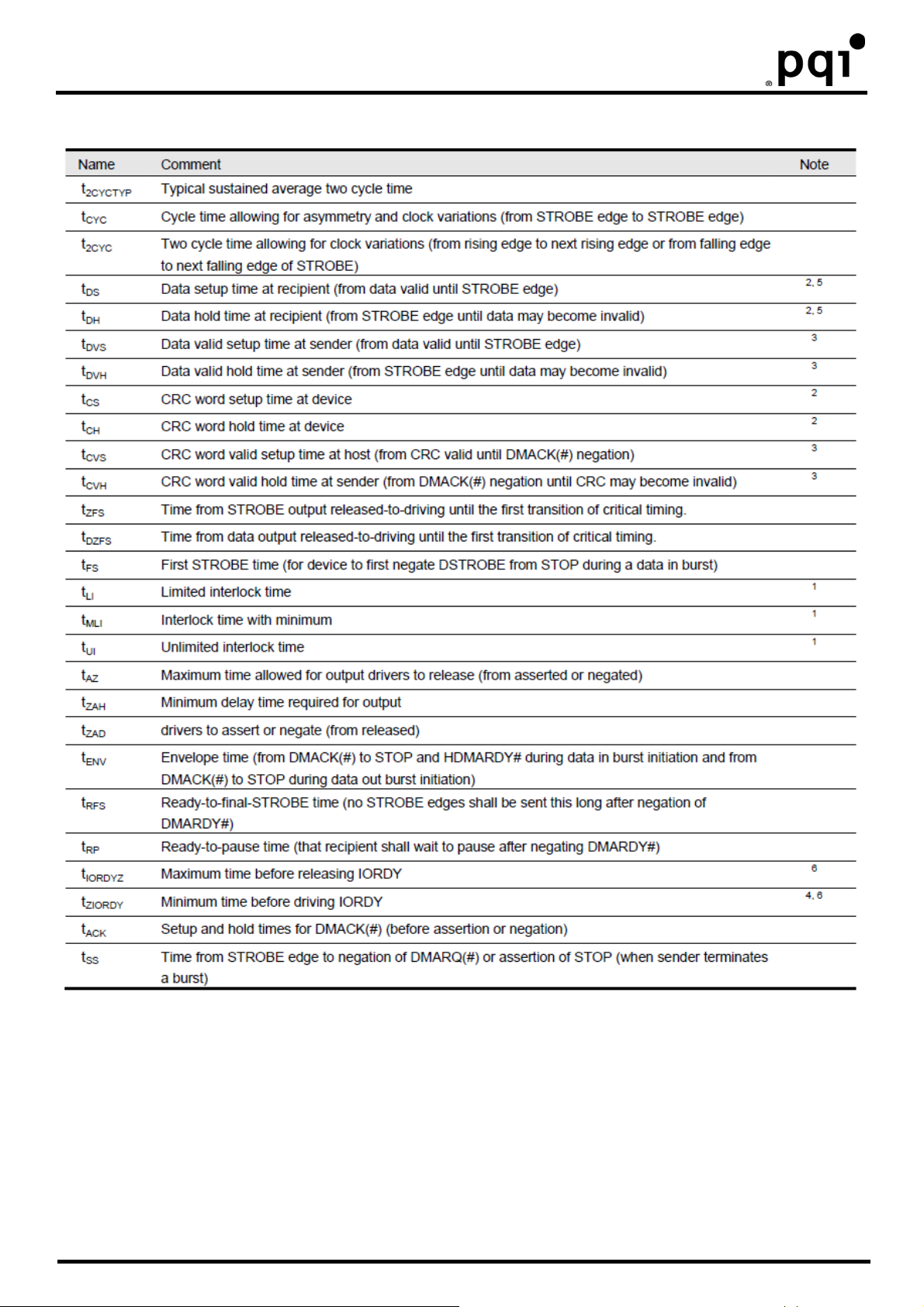
7.11 Ultra DMA Data Burst Timing Descriptions
Rev. A.1 43/50 July. 2010
Page 48

CompactFlash Card
7.12 Ultra DMA Sender and Recipient IC Timing Requirements
7.13 Ultra DMA AC Signal Requirements
Rev. A.1 44/50 July. 2010
Page 49

CompactFlash Card
Ultra DMA Data-In Burst Initiation Timing
Sustained Ultra DMA Data-in Burst Timing
Rev. A.1 45/50 July. 2010
Page 50

CompactFlash Card
Ultra DMA Data-In Burst Host Pause Timing
Ultra
DMA
Data-in Burst Host Pause Timing
Rev. A.1 46/50 July. 2010
Page 51

CompactFlash Card
Ultra DMA Data-in Burst Device Termination Timing
Ultra DMA Data-in Burst Host Termination Timing
Rev. A.1 47/50 July. 2010
Page 52

CompactFlash Card
Ultra DMA Data-out Burst initiation Timing
Sustained Ultra DMA Data-Out Burst Timing
Rev. A.1 48/50 July. 2010
Page 53

CompactFlash Card
Ultra DMA Data-Out Burst Device Pause Timing
Ultra DMA Data-Out Burst Device Termination Timing
Rev. A.1 49/50 July. 2010
Page 54

CompactFlash Card
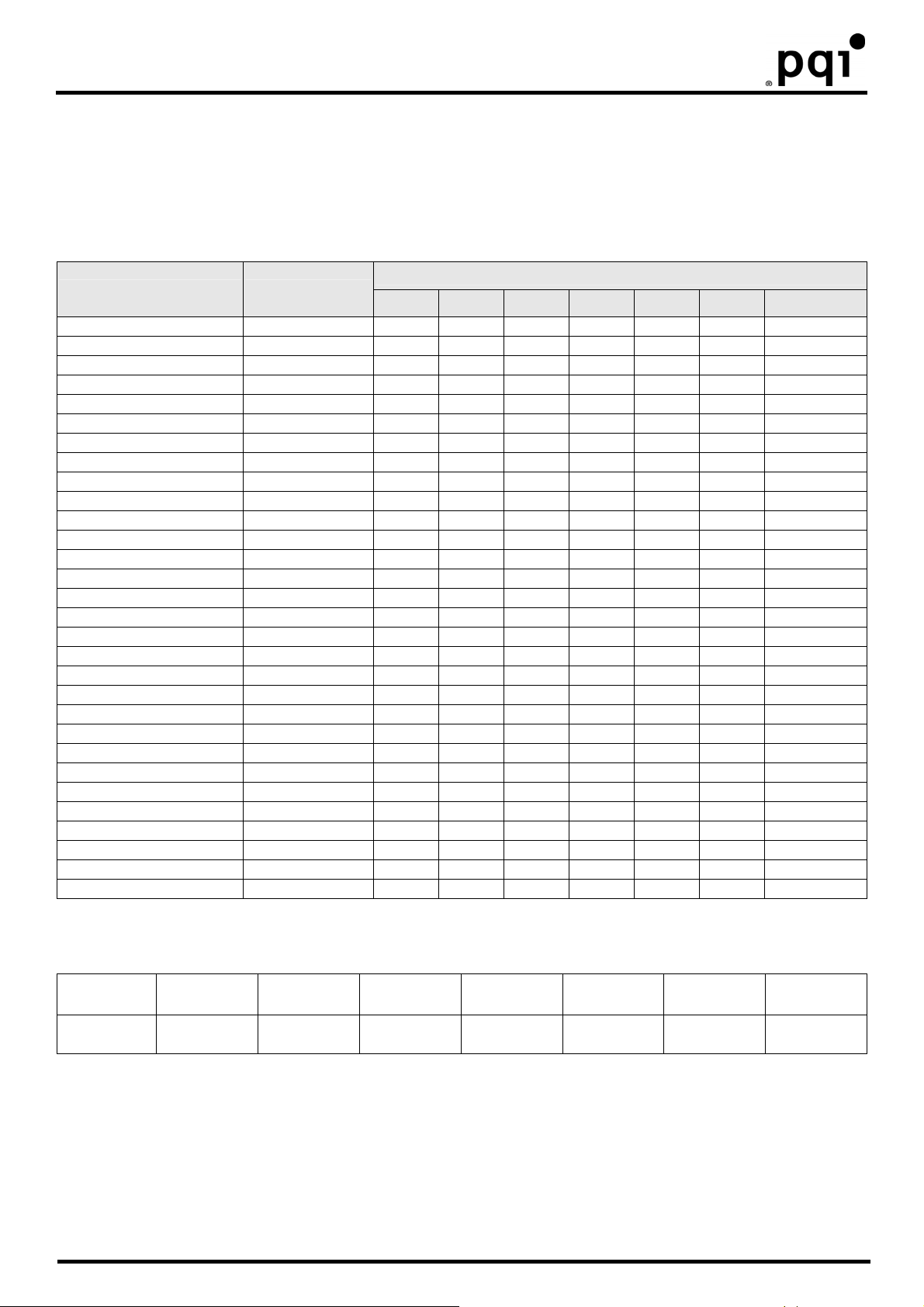
9. Physical outline
Ultra DMA Data-Out Burst Host Termination Timing
Rev. A.1 50/50 July. 2010
 Loading...