

Page 1
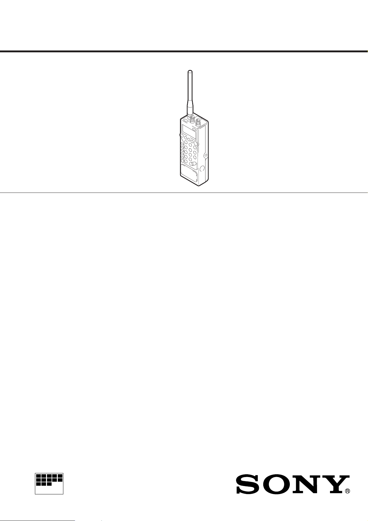
ICF-SC1/SC1PC
SERVICE MANUAL
Ver 1.0 1998.03
SPECIFICATIONS
Circuit system :
Frequency range :
Detection mode :
Speaker : Approx. 36 mm (1 7/16 inches) dia., 8 ohms
Power output :
Output : @ jack (monaural minijack)
Power requirements :
External power source :
Dimensions :
Mass : Approx. 252g (8.9 oz)
Triple conversion superheterodyne
25.000 – 1300.000MHz
(excluding cellular phone band : 823.980 – 849.020 MHz and
868.980 – 894.020 MHz)
AM, NFM, WFM
150mW(at 10% harmonic distortion
DC 6V, four size AA (R6) batteries
DC 6V
Approx. 64 x 177 x 44.3 mm (w/h/d) (2 5/
incl. projecting parts and controls, not including the helical
antenna and the belt holder
Approx. 382g (13.5 oz) incl. alkaline batteries, helical
antenna, and the belt holder
8
x 7 x 1 3/4 inches)
US Model
Supplied Accessories
AC power adaptor (1)
Earphone (1)
Belt holder (1)
Helical antenna (1)
Frequency guidebook (1)
CD-ROM (1) (ICF-SC1PC only)
Serial port connecting cable (1) (ICF-SC1PC only)
Clamp filter (1) (ICF-SC1PC only)
Design and specifications are subject to change without notice.
MICROFILM
PLL SYNTHESIZED SCANNING RECEIVER
Page 2

TABLE OF CONTENTS
Specifications ........................................................................... 1
1. GENERAL
Location and Function of Controls .................................... 3
2. DISASSEMBLY
2-1. Helical Antenna Removal......................................... 10
2-2. Cabinet (Rear) Assy Removal .................................. 10
2-3. Microcomputer Board, IF Board,
RF Board Removal ....................................................11
3. TEST MODE................................................................ 12
4. ELECTRICAL ADJUSTMENS .............................. 13
5. DIAGRAMS
5-1. Explanation of IC Terminals .................................. 15
5-2. Block Diagram....................................................... 17
5-3. Printed Wiring Boards – IF Section– ..................... 19
5-4. Schematic Diagram – IF Section– ......................... 21
5-5. Printed Wiring Boards – Microcomputer Section– 23
5-6. Schematic Diagram – Microcomputer Section–.... 25
5-7. Printed Wiring Boards – RF Section –................... 27
5-8. Schematic Diagram – RF Section (1/2) – .............. 39
5-9. Schematic Diagram – RF Section (2/2) – .............. 31
6. EXPLODED VIEW..................................................... 35
7. ELECTRICAL PARTS LIST.................................... 36
SAFETY-RELATED COMPONENT WARNING!!
COMPONENTS IDENTIFIED BY MARK ! OR DOTTED LINE WITH
MARK ! ON THE SCHEMATIC DIAGRAMS AND IN THE PARTS
LIST ARE CRITICAL TO SAFE OPERATION.
REPLACE THESE COMPONENTS WITH SONY PARTS WHOSE
PART NUMBERS APPEAR AS SHOWN IN THIS MANUAL OR IN
SUPPLEMENTS PUBLISHED BY SONY.
– 2 –
Page 3
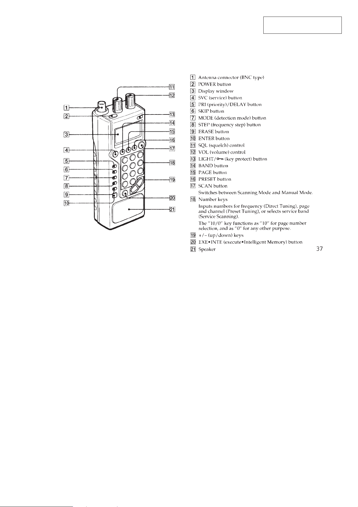
LOCATION AND FUNCTION OF CONTROLS
FRONT
SECTION 1
GENERAL
This section is extracted from
instruction manual.
– 3 –
Page 4
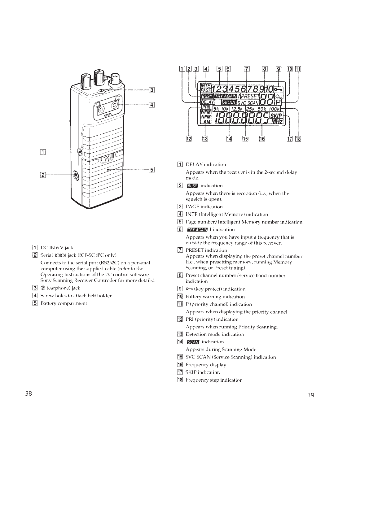
SIDE/REAR DISPLAY
– 4 –
Page 5
– 5 –
Page 6
– 6 –
Page 7
– 7 –
Page 8
– 8 –
Page 9
– 9 –
Page 10
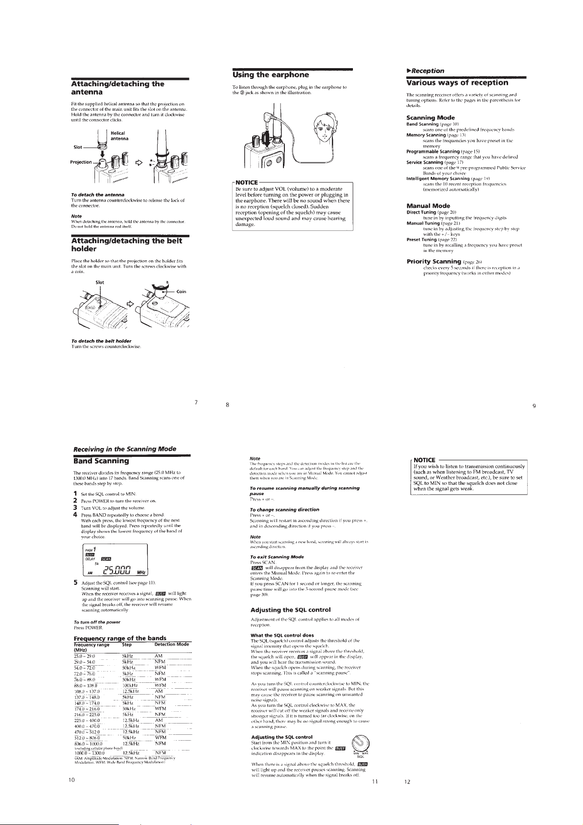
SECTION 2
y
DISASSEMBLY
Note : Follow the disassembly procedure in the numerical order given.
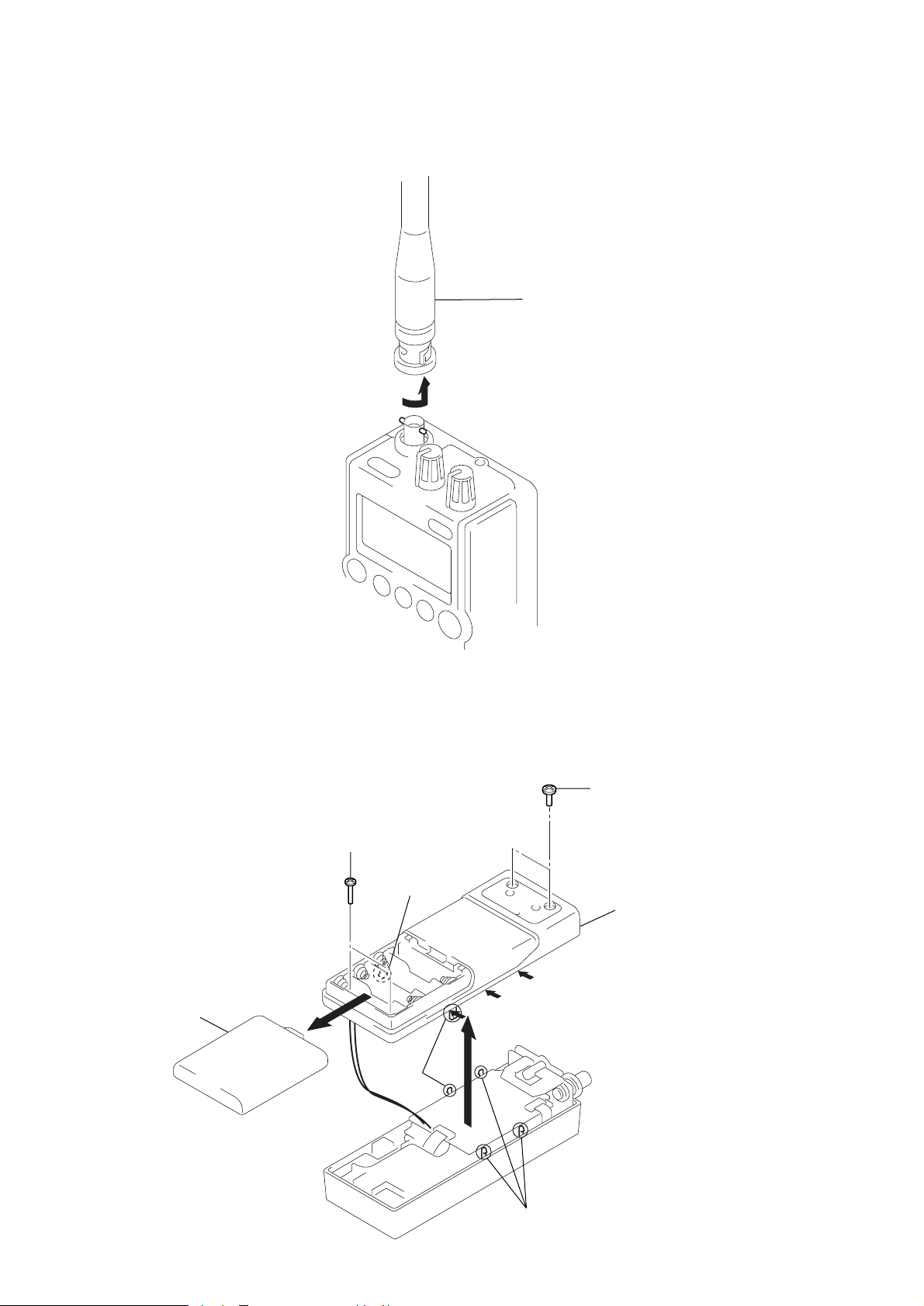
2-1. HELICAL ANTENNA REMOVAL
1
Helical antenna
2-2. CABINET (REAR) ASSY REMOVAL
Battery case lid
1
2
Screws
Claw
Claws
3
4
3
3
2
Screws
Cabinet (Rear) ass
– 10 –
Claws
Page 11
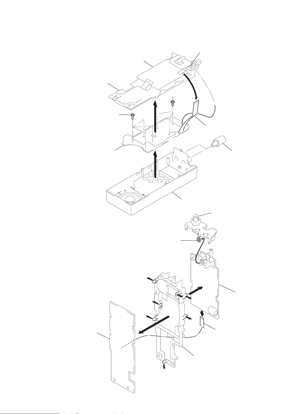
2-3. MICROCOMPUTER BOARD, IF BOARD, RF BOARD REMOVAL
d
)
IF board
RF board
5
Screws
4
5
Screws
2
Remove solder
3
CN402 (22pin)
Microcomputer board
6
7
Remove solder
!™
!º
Cabinet (Front) assy
8
!¡
!™
!º
1
Knob (VOL
Coaxial connector
IF boar
RF board
!™
!£
– 11 –
!™
!º
9
CN401 (16pin)
Chassis
Page 12

SECTION 3
TEST MODE
Reading the S-Curve voltage for scan-stop
The ICF-SC1 and SC1PC have a scan-stop function used to scan
for the correct frequency.
Scanning continues until the squelch turns off (when a signal is
received). However, just setting the squelch off as condition does
not guarantee that the scan-stop function will always stop at the
correct frequency. (It might for instance deviate 1 step to an adjacent frequency.)
So scan-stop is set to trigger only at the correct frequency, by checking the DC voltage component (S-curve voltage) of the FM detector output.
The DC voltage component of the FM detector output may vary
however, due to variations in the parts components of the FM detector circuit or deviations in the local oscillator frequency . Therefore, once repair or alignment is complete, read the DC voltage
component of the RF detector output while it is input with an IF
signal from a signal generator, and use that value as a reference to
write data on the EEPROM.
Two types of writing are performed on the EEPROM since there
are two types of FM detectors.
WFM n for WFM
NFM n for NFM, AM
Refer to the following for information on the write method and on
the signal input method using a signal generator.
S-Curve voltage write method
Signal input method using signal generator.
1. In NFM
TP1
C407
1000P
16
IN
0.01µ
S.G.
45M X'tal filter
IC401
TA31136FN
MIX
(1) Connect a signal generator to TP1 by way of a 0.01µF capaci-
tor.
(2) Receive NFM (Receive frequency does no matter)
(3) Input 455kHz from the signal generator, 90 to 100dBµ, modu-
lation 30%, mod frequency of 1kHz.
(4) Write the COMPN terminal voltage onto the ROM.
(5) Press the [SVC] button.
When data is written, a display as shown below appears.
NFM
0.94
LCD (all lamps on)
All LCD lamps up when the three [EXE], [–] and [SCAN] keys are
simultaneously held down while the power is off.
Reading the S-Curve voltage component
1. Input method for S-Curve voltage component read mode
Simultaneously hold down the [MODE], [STEP] and [BAND] keys
for at least 1second while power is off.
The set (ICF-SC1/SC1PC) power turns on and a display as shown
below appears.
2. Quitting S-Curve voltage read mode
Press the [POWER] button.
Note : When set in S-Curve voltage read mode, do not connect any-
thing to the antenna terminal while the power to the RF section is on. (An unwanted signal might otherwise be received
through the antenna.)
However when set, a check can be made that a broadcast RF carrier
wave was received.
(1) Turn the power on as usual and receive a broadcast signal.
(2) Turn off the power and set in read mode with [MODE] + [STEP]
+ [BAND].
(3) Write can be checked with [SVC] or [SCAN] since the broad
cast signal received in (1) can be heard.
Voltage (V)
2. In WFM
TP4
C434
0.01µ
10
RF BOARD
0.01µ
S.G.
IC402
CXA1111N
FM RF
IN
(1) Connect a signal generator to TP4 by way of a 0.01µF capaci-
tor.
(2) Receive WFM (Receive frequency does no matter)
(3) Input 10.7MHz from the signal generator, 90 to 100dBµ, fre-
quency deviation 22.5kHz, mod frequency of 1kHz.
(4) Write the COMPW terminal voltage onto the ROM.
(5) Press the [SCAN] button.
When data is written, a display as shown below appears.
WFM
0.87
Voltage (V)
Adjustment Location :
[ IF BOARD] (Rear side)
In the following cases the message “TRY AGAIN” appears and
writing is disabled.
(1) When the Squelch is closed.
(2) When the S-curve voltage that was read, is not within 0.5V to
1.3V.
CN402
COMPN
COMPW
– 12 –
Page 13

SECTION 4
ELECTRICAL ADJUSTMENTS
Setting :
trackig generator
(GND)
spectrum analyzer
(GND)
FM RF signal
generator
(GND)
digital
voltmeter
(GND)
RF BOARD (SINGLE) ADJUSTMENT
1. 2nd local oscillator Adjustment
Procedure :
(1) Connect a tracking generator to TP10 and a spectrum ana-
lyzer to TP6.
(TG level = – 40 to – 50dBm, spectrum analyzer span =
200MHz)
(2) Receive a 600MHz signal.
(3) Repeatedly adjust CT303, 304 and 305 for an optimal wave-
form at center frequency of 277.5MHz.
(4) Receive the 25MHz signal.
(5) Adjust the 2nd local oscillator to 555MHz with CT302.
(spectrum analyzer span = 10kHz)
2. 1st local oscillator Adjustment
Procedure :
(1) Connect a spectrum analyzer to TP5.
(2) Receive a 767.5MHz signal.
(3) Adjust the CT301 so that 1st local oscillator = 1000MHz
(spectrum analyzer span = 10kHz)
3. 1st IF (low) Adjustment
Procedure :
(1) Connect a tracking generator to TP5 and a spectrum analyzer
to TP7.
(2) Recive a 500MHz signal.
(3) Repeatedly adjust CT201, 202 and 203 for an optimal wave-
form (ladder shape) at center frequency of 232.5MHz.
(TG level = – 30 to – 40dBm, spectrum analyzer span =
200MHz)
IF BOARD (SINGLE) ADJUSTMENT
1. 3rd local oscillator Adjustment
Procedure :
(1) Connect a spectrum analyzer to TP2.
(2) Receive a 49.975MHz signal.
(3) Adjust the CT401 so that the 3rd local oscillator =
44.5500MHz. (spectrum analyzer span = 10kHz)
(4) Recive a 50.0125MHz signal.
(5) Adjust the 3rd local oscillator to 44.5425MHz with RV401.
(spectrum analyzer span = 10kHz)
Adjustment Location : IF board (see page 14)
RF & IF BOARD (COMBINATION) ADJUSTMENT
1. 2nd IF (narrow) Adjustment
Procedure :
(1) Connect a tracking generator to RF (RF board) TP6 and con-
nect a spectrum analyzer to IF (IF board) TP1 by way of a
0.5pF capacitor.
(2) Receive a 29MHz signal.
(3) Align for an optimal waveform with T206.
(ladder waveform with minimum ripple)
(TG level = – 50dBm, spectrum analyzer Center freq. =
45MHz, span = 100kHz)
2. 2nd IF (wide) Adjustment
Procedure :
(1) Connect a tracking generator to RF (RF board) TP6 and con-
nect a spectrum analyzer to IF (IF board) TP3.
(2) Receive a 70MHz signal.
(3) Adjust so the 45MHz is at maximum by using CT402 and
T205.
(TG level = – 50dBm, spectrum analyzer Center freq. =
45MHz, span = 50MHz)
3. AGC Adjustment
Procedure :
(1) Connect a FM RF signal generator to the BNC (ANT IN)
connector.
(2) Connect a digital voltmeter to RV403 center tap (COMMON).
(IF board)
(3) Receive a 122MHz signal (input level 80d µEMF, AM, modu-
lation 30%).
(4) Adjust RV403 so that digital voltmeter reading is at 1.68 ±
0.02V.
Adjustment Location : RF, IF board (see page 14)
* Use semirigid cable when connecting the tracking generator and
spectrum analyzer to the circuit board.
* Spectrum analyzer settings shown in the ( ) are reference values.
Adjustment Location : RF board (see page 14)
– 13 –
Page 14

Adjustmen Location :
[RF BOARD] (Front side)
TP2
TP3
TP6
TP7
TP5
TP1
[RF BOARD] (Rear side)
ANT IN
(BNC connector)
[ IF BOARD] (Rear side)
CT301
CT201
CT202
CT305
CT203
CT304
T206
T205
TP10
CT303
CT302
RV403 center tap
(COMMON)
GND
TP1
RV403
RV401
TP4
TP3
TP2
CT401
CT402
– 14 –
GND
Page 15

SECTION 5
DIAGRAMS
5-1. EXPLANATION OF IC TERMINALS
IC604 µPD78064BGC (SYSTEM CONTROL)
Pin No. Pin name I/O Description
1 COMP-W I WFM S-curve voltage input (A/D input).
2 BATT I Low battery voltage detection input (A/D input).
3 – 7 KS0 – 4 O Key matrix output.
8 AVDD – Power supply for A/D converter.
9 AVREF – Power supply for A/D reference.
10 AC-DET I External power supply detect terminal.
11 LED O LED drive. “H” : Lighting
12 VSS – Ground.
13 TEST I Test mode terminal. “H” : Test mode
14 LCD I “H” : Normal. (LCD display ON = H during PC operaion)
15 BEEP O Beep signal output.
16 SCAN O Scan signal output. “H” : Scan run
17 DUB – Not used (Open).
18 WFM O WFM mode select. “H” : WFM mode
19 D/A 0 O D/A output bit 0 for minute step.
20 D/A 1 O D/A output bit 1 for minute step.
21 STANDBY O Standby signal output. “H” : RS232C interface OFF
22 MUTE O Mute signal output. “H” : Mute ON
23 – 25 COM0 – 2 O LCD common output.
26 COM3 – Not used (Open).
27 BIAS – LCD bias terminal.
28 – 30 VLC0 – 2 – LCD bias terminal.
31 VSS – Ground.
32 – 62 S0 – 30 O LCD segment output.
63 – Not used (Open).
64 AM O AM mode output. “H” : AM mode
65 NFM O NFM mode output. “H” : NFM mode
66 IF 1 O IF selection output.
67 RF O RF selection output.
68 MAIN O Main power supply ON/OFF control.
69 FILTER O Serial latch output for filter selection.
70 PLL O Serial latch output for PLL selection.
71 ROM O Clock output for EEPROM.
72 DO I Serial data input from EEPROM.
73 DI O Serial data output to EEPROM.
74 CLK O Serial clock output.
75 RXD I RXD input from RS232C interface.
76 TXD O TXD output to RS232C interface.
77 CTS O CTS output to RS232C interface.
78 IC (GND) – Ground.
79 XM2 Main clock oscillator (4.194304MHz).
80 XM1 Main clock oscillator (4.194304MHz).
81 VDD – Power supply (+4.0V).
82 XS2 Sub clock oscillator (32.768kHz).
83 XS1 Sub clock oscillator (32.768kHz).
84 RESET I System reset terminal.
85 OFF-DET I Low power detection OFF input. “L” : OFF
– 15 –
Page 16

Pin No. Pin name I/O Description
86 L-DET I PLL lock detect. “L” : Lock
87 N-DET I Squelch detection input. “L” :
88 RTS I RTS input from RS232C interface.
89 CONNECT I PC connect check signal input.
90 REMOTE I PC connect check signal input.
91 – Not used (Open).
92 – Not used (Open).
93 – 98 KR5 – 0 I Key matrix input.
99 VSS – Ground.
100 COMP-N I NFM (AM) S-curve voltage input (A/D input).
– 16 –
Page 17

5-2. BLOCK DIAGRAM
ICF-SC1/SC1PC
– 17 – – 18 –
• Signal path.
F
Page 18

5-4. SCHEMATIC DIAGRAM – IF SECTION –
r
Refer to page 33 for IC Block Diagrams.
ICF-SC1/SC1PC
Note:
• All capacitors are in µF unless otherwise noted. pF: µµF
50 WV or less are not indicated except for electrolytics
and tantalums.
• All resistors are in Ω and 1/
specified.
• U : B+ Line.
• Power voltage is dc 6 V and fed with regulated dc power
supply from external power voltage jack (J402).
• Voltages are dc with respect to ground under no-signal
(detuned) conditions.
no mark : WFM/AM/NFM
( ) : AM/NFM
< > : NFM
4
W or less unless otherwise
• Voltages are taken with a VOM (Input impedance 10 MΩ).
Voltage variations may be noted due to normal production tolerances.
• Signal path.
F
– 21 – – 22 –
Page 19

p
p
5-6. SCHEMATIC DIAGRAM – MICROCOMPUTER SECTION –
r
Refer to page 33 for IC Block Diagrams.
ICF-SC1/SC1PC
Note:
• X : parts extracted from the component side.
• D : Chip components extracted from the rear side.
r
•
• b : Pattern from the side which enables seeing.
(The other layers' patterns are not indicated.)
Caution:
Pattern face side: Parts on the pattern face side seen from
(Conductor Side) the pattern face are indicated.
Parts face side: Parts on the parts face side seen from
(Component Side) the parts face are indicated.
: Through hole.
r
Note:
• All capacitors are in µF unless otherwise noted. pF: µµF
50 WV or less are not indicated except for electrolytics
and tantalums.
• All resistors are in Ω and 1/
specified.
• U : B+ Line.
• Power voltage is dc 6 V and fed with regulated dc power
supply from external power voltage jack (J402).
• Voltages and waveforms are dc with respect to ground
under no-signal (detuned) conditions.
no mark : WFM/AM/NFM
( ) : AM/NFM
< > : NFM
4
W or less unless otherwise
• Voltages are taken with a VOM (Input impedance 10 MΩ).
Voltage variations may be noted due to normal production tolerances.
• Waveforms are taken with a oscilloscope.
Voltage variations may be noted due to normal production tolerances.
• Circled numbers refer to waveforms.
WAVEFORMS
1
32.7 µsec
IC604 *™
VOL T/DIV : 0.2 V AC
TIME/DIV : 20 msec
– 25 – – 26 –
0.5Vp-
2
2Vp-
0.24 µsec
IC604 &ª
VOLT/DIV : 1 V AC
TIME/DIV : 0.2 msec
Page 20

ICF-SC1/SC1PC
5-8. SCHEMATIC DIAGRAM – RF SECTION (1/2) –
r
Refer to page 33 for IC Block Diagrams.
Note:
• X : parts extracted from the component side.
• D : Chip components extracted from the rear side.
r
•
• b : Pattern from the side which enables seeing.
(The other layers' patterns are not indicated.)
Caution:
Pattern face side: Parts on the pattern face side seen from
(Conductor Side) the pattern face are indicated.
Parts face side: Parts on the parts face side seen from
(Component Side) the parts face are indicated.
: Through hole.
Note:
• All capacitors are in µF unless otherwise noted. pF: µµF
50 WV or less are not indicated except for electrolytics
and tantalums.
• All resistors are in Ω and 1/
specified.
• U : B+ Line.
• Power voltage is dc 6 V and fed with regulated dc power
supply from external power voltage jack (J402).
• Voltages are dc with respect to ground under no-signal
(detuned) conditions.
no mark : WFM/AM/NFM
( ) : AM/NFM
< > : NFM
• Voltages are taken with a VOM (Input impedance 10 MΩ).
Voltage variations may be noted due to normal production tolerances.
• Signal path.
F
4
W or less unless otherwise
– 29 – – 30 –
Page 21

ICF-SC1/SC1PC
5-9. SCHEMATIC DIAGRAM – RF SECTION (2/2) –
r
Refer to page 33 for IC Block Diagrams.
Note:
• All capacitors are in µF unless otherwise noted. pF: µµF
50 WV or less are not indicated except for electrolytics
and tantalums.
• All resistors are in Ω and 1/
specified.
• U : B+ Line.
• Power voltage is dc 6 V and fed with regulated dc power
supply from external power voltage jack (J402).
• Voltages are dc with respect to ground under no-signal
(detuned) conditions.
no mark : WFM/AM/NFM
( ) : AM/NFM
< > : NFM
• Voltages are taken with a VOM (Input impedance 10 MΩ).
Voltage variations may be noted due to normal production tolerances.
• Signal path.
F
4
W or less unless otherwise
– 31 – – 32 –
Page 22

r
24 23 22 21 20 19 18 17 16 15 14 13
1 2 3 4 5 6 7 8 9 10 11 12
FM.IF
DISCRI
TUNING
METER
RIPPLE
FILTER
AM.IF
DET.AGC
BAND SIGNAL
OUTPUT CIRCUIT
REGULATOR
FM.FE
AM.FE
BAND
AM IF
FM IF
TUNE
EARTH
IF
AFCW
AFCJ
DET
FILTER
VCC
MUTE
MIX OUT
EARTH
FM IN
NC
AM RF
FM RF
REG
FM OSC
AFC
AM OSC
DISCRI
EARTH
IC BLOCK DIAGRAMS
IC301 MB1511-PFV-EF
NC∅R∅P
20 19 18
PHASE
COMPARATPR
SWITCH
BINARY 14BIT
REFERENCE
COUNTER
OSCILLATOR
213 4
NC
OSC I
F OSC
17 16 15 14 13 12 11
MONITOR FREQUENCY
SELECT CIRCUIT
15BIT
LATCH
OSC O
CHAGE
PUMP
SIFT RESISTER
VP
16BIT
VCC
SW
6578
DO
ANALOG
SWITCH
LD
GND
FC
19BIT
SIFT RESISTER
LE
DATANCCLKF IN
CONTROL
1BIT
LATCH
BINARY 11BIT
PROGRAMABLE
COUNTER
18BIT
LATCH
PRESCALER
CIRCUIT
910
NC
BINARY 7BIT
SWALLOW
COUNTER
IC402 CXA1111NIC401 TA31136FN
CONTROL
CIRCUIT
MIX IN
GND
N-REC
N-DET
RSSI
IF OUT
IF IN
11
RSSI
QUADRATURE
IF AMP
DEC
16 15 14 13 12
MIXER
NOISE
COMPARATOR
DETECTOR
BUFFER
LOCAL
OSCILLATION
2 345 6 7 8
1
OSC IN
MIX OUT
OSC OUT
VCC
IC407 CXA1522N
IN1
16
1
IN2
15 14 13 12 11 10 9
REG VOL
REG
2
NC
3
VOL
NC
NF1
4
NF2
QUAD
L.P.F
FILTER
AMP
FIL IN
GND1
PRE+POWER1
PRE+POWER2
GND2
AF OUT
9
P-GND1
P-GND2
OUT1
OUT2
10
DETECTION
NOISE
AMP
FIL OUT
5678
VCC
RIPPLE
– 33 –
Page 23

STATUS
REGISTER
OUTPUT
BUFFER
VCC
MEMORY ARRAY
1024/2048/
4096/8192X8
1
HOLD
CLOCK
GENERATOR
DATA
REGISTER
MODE
DECODE
LOGIC
2 3 4
CS
SO
WP
SCK
ADDRESS
DECODER
IC607 µ PD4721GS-GJG-E2 (ICF-SC1PC)IC605 AT25160N-10SC2.7T2.5
SI
5678
GND
C4+
GND
C4–
VSS
STBY
VCHA
C5+
C5 –
DOUT1
DIN1
20
21931841751661571481391210
1
C1+
C1–
VCC
VDD
DOUT2
DIN2
RIN1
ROUT1
RIN2
11
ROUT2
– 34 –
Page 24

NOTE :
#1
#2
#3
LCD601
ANT101
SP401
1
2
3
4
28
5
6
7
8
9
10
11
12
13
14
15
16
17
17
17
17
18
19
20
21
23
24
25
26
27
30
31
32
33
34
35
36
37
29
22
(including rA)
r
A
• -XX, -X mean standardized parts, so they
may have some difference from the original
one.
• Items marked “ * ”are not stocked since they
are seldom required for routine service. Some
delay should be anticipated when ordering
these items.
SECTION 6
EXPLODED VIEW
• The mechanical parts with no reference
number in the exploded views are not
supplied.
• Hardware (# mark) list and accessories and
packing materials are given in the last of this
parts list.
(SC1PC)
Ref. No. Part No. Description Remark Ref. No. Part No. Description Remark
1 X-3375-048-1 CABINET (FRONT) ASSY (SC1)
1 X-3375-049-1 CABINET (FRONT) ASSY (SC1PC)
2 3-020-649-01 SHEET (SPEAKER)
3 3-020-631-01 GRILLE (SPEAKER) (SC1)
3 3-020-631-11 GRILLE (SPEAKER) (SC1PC)
4 4-942-636-01 EMBLEM (NO.3.5), SONY
5 3-907-103-11 SPRING, RING
6 3-020-641-01 KNOB (VOL)
7 3-020-629-01 BUTTON (POWER)
8 3-020-628-01 BUTTON (LIGHT)
9 1-771-359-11 SWITCH, RUBBER KEY
* 10 A-3679-948-A MICROCOMPUTER BOARD, COMPLETE
* 10 A-3679-949-A MICROCOMPUTER BOARD, COMPLETE (SC1)
11 3-020-633-01 CASE (LCD)
* 12 3-025-927-01 SPACER (B)
13 1-694-377-11 CONDUCTIVE BOARD, CONNECTION
14 3-020-632-01 PLATE, LIGHT GUIDE
15 3-024-792-01 PLATE, CONTACT
16 1-783-112-11 CORD
17 3-713-790-21 SCREW (M2X6), TAPPING, P3
* 18 3-026-576-01 CUSHION (D)
* 19 A-3679-950-A RF BOARD, COMPLETE
* 20 3-020-634-01 CHASSIS
21 1-783-379-11 CABLE, FLEXIBLE FLAT (22 CORE)
22 3-025-928-01 CUSHION (A)
23 3-020-636-01 LUG (BNC)
24 3-020-637-01 FRAME
25 3-020-635-01 RING (BNC) (SC1)
25 3-020-635-11 RING (BNC) (SC1PC)
26 1-784-075-11 CONNECTOR, COAXIAL (BNC TYPE)
27 3-025-438-01 SPACER (C)
28 3-020-640-01 LED, BATTERY CASE (SC1)
28 3-020-640-11 LED, BATTERY CASE (SC1PC)
* 29 A-3679-951-A IF BOARD, COMPLETE
* 30 3-026-273-01 CUSHION (B)
31 4-860-518-00 CUSHION
32 1-783-378-11 CABLE, FLEXIBLE FLAT (16 CORE)
33 3-020-639-01 CABINET (REAR) (SC1)
33 3-020-639-11 CABINET (REAR) (SC1PC)
34 3-907-747-01 SPRING (+/-.B), BATTERY
35 3-919-944-01 TERMINAL (+), BATTERY
36 3-907-746-01 SPRING (+/-.A), BATTERY
37 3-020-638-01 TERMINAL (-), BATTERY
ANT101 1-501-969-11 ANTENNA, HELICAL
LCD601 1-803-003-11 DISPLAY PANEL, LIQUID CRYSTAL
SP401 1-505-872-11 SPEAKER (3.6cm)
– 35 –
Page 25

SECTION 7
IF
NOTE :
• Due to standardization, replacements in the
parts list may be different from the parts
specified in the diagrams or the components
used on the set.
• -XX, -X mean standardized parts, so they
may have some difference from the original
one.
• RESISTORS
All resistors are in ohms
METAL : Metal-film resistor
METAL OXIDE :Metal oxide-film resistor
F : nonflammable
• Items marked “ * ”are not stocked since
they are seldom required for routine service.
Some delay should be anticipated when
ordering these items.
Ref. No. Part No. Description Remark Ref. No. Part No. Description Remark
* A-3679-951-A IF BOARD, COMPLETE
******************
< CAPACITOR >
C401 1-162-906-11 CERAMIC CHIP 1.5PF 0.25PF 50V
C402 1-162-912-11 CERAMIC CHIP 7PF 0.5PF 50V
C403 1-162-964-11 CERAMIC CHIP 0.001uF 10% 50V
C405 1-162-970-11 CERAMIC CHIP 0.01uF 10% 25V
C406 1-162-970-11 CERAMIC CHIP 0.01uF 10% 25V
C407 1-164-357-11 CERAMIC CHIP 1000PF 5% 50V
C408 1-162-964-11 CERAMIC CHIP 0.001uF 10% 50V
C409 1-162-964-11 CERAMIC CHIP 0.001uF 10% 50V
C410 1-107-826-11 CERAMIC CHIP 0.1uF 10% 16V
C411 1-164-382-11 CERAMIC CHIP 91PF 5% 50V
C412 1-162-964-11 CERAMIC CHIP 0.001uF 10% 50V
C413 1-162-970-11 CERAMIC CHIP 0.01uF 10% 25V
C414 1-162-920-11 CERAMIC CHIP 27PF 5% 50V
C415 1-162-912-11 CERAMIC CHIP 7PF 0.5PF 50V
C416 1-162-964-11 CERAMIC CHIP 0.001uF 10% 50V
C417 1-135-259-11 TANTAL. CHIP 10uF 20% 6.3V
C418 1-107-826-11 CERAMIC CHIP 0.1uF 10% 16V
C419 1-162-927-11 CERAMIC CHIP 100PF 5% 50V
C420 1-162-927-11 CERAMIC CHIP 100PF 5% 50V
C422 1-162-968-11 CERAMIC CHIP 0.0047uF 10% 50V
C423 1-162-964-11 CERAMIC CHIP 0.001uF 10% 50V
C424 1-107-826-11 CERAMIC CHIP 0.1uF 10% 16V
C425 1-115-156-11 CERAMIC CHIP 1uF 10V
C426 1-162-970-11 CERAMIC CHIP 0.01uF 10% 25V
C427 1-162-970-11 CERAMIC CHIP 0.01uF 10% 25V
C428 1-162-970-11 CERAMIC CHIP 0.01uF 10% 25V
C429 1-162-970-11 CERAMIC CHIP 0.01uF 10% 25V
C430 1-162-970-11 CERAMIC CHIP 0.01uF 10% 25V
C431 1-162-919-11 CERAMIC CHIP 22PF 5% 50V
C432 1-164-357-11 CERAMIC CHIP 1000PF 5% 50V
C433 1-162-919-11 CERAMIC CHIP 22PF 5% 50V
C434 1-162-970-11 CERAMIC CHIP 0.01uF 10% 25V
C435 1-162-970-11 CERAMIC CHIP 0.01uF 10% 25V
C436 1-135-259-11 TANTAL. CHIP 10uF 20% 6.3V
C437 1-162-920-11 CERAMIC CHIP 27PF 5% 50V
C438 1-162-970-11 CERAMIC CHIP 0.01uF 10% 25V
C439 1-162-970-11 CERAMIC CHIP 0.01uF 10% 25V
C440 1-162-964-11 CERAMIC CHIP 0.001uF 10% 50V
C441 1-135-181-21 TANTAL. CHIP 4.7uF 20% 6.3V
ELECTRICAL PARTS LIST
• SEMICONDUCTORS
In each case, u : µ , for example :
uA.... : µ A.... , uPA.... : µ PA....
uPB.... : µ PB.... , uPC.... : µ PC....
uPD.... : µ PD....
• CAPACITORS
uF : µ F
• COILS
uH : µ H
C442 1-115-156-11 CERAMIC CHIP 1uF 10V
C443 1-162-959-11 CERAMIC CHIP 330PF 5% 50V
C444 1-135-259-11 TANTAL. CHIP 10uF 20% 6.3V
C445 1-162-970-11 CERAMIC CHIP 0.01uF 10% 25V
C446 1-124-779-00 ELECT CHIP 10uF 20% 16V
C447 1-115-156-11 CERAMIC CHIP 1uF 10V
C448 1-115-156-11 CERAMIC CHIP 1uF 10V
C449 1-162-927-11 CERAMIC CHIP 100PF 5% 50V
C450 1-162-966-11 CERAMIC CHIP 0.0022uF 10% 50V
C451 1-164-156-11 CERAMIC CHIP 0.1uF 25V
C452 1-115-156-11 CERAMIC CHIP 1uF 10V
C453 1-162-970-11 CERAMIC CHIP 0.01uF 10% 25V
C454 1-164-357-11 CERAMIC CHIP 1000PF 5% 50V
C455 1-115-156-11 CERAMIC CHIP 1uF 10V
C456 1-124-779-00 ELECT CHIP 10uF 20% 16V
C457 1-162-970-11 CERAMIC CHIP 0.01uF 10% 25V
C458 1-107-826-11 CERAMIC CHIP 0.1uF 10% 16V
C459 1-107-826-11 CERAMIC CHIP 0.1uF 10% 16V
C460 1-107-826-11 CERAMIC CHIP 0.1uF 10% 16V
C461 1-128-394-11 ELECT CHIP 220uF 20% 10V
C462 1-164-156-11 CERAMIC CHIP 0.1uF 25V
C463 1-164-245-11 CERAMIC CHIP 0.015uF 10% 25V
C464 1-164-346-11 CERAMIC CHIP 1uF 16V
C465 1-107-826-11 CERAMIC CHIP 0.1uF 10% 16V
C466 1-107-826-11 CERAMIC CHIP 0.1uF 10% 16V
C467 1-124-778-00 ELECT CHIP 22uF 20% 6.3V
C468 1-128-394-11 ELECT CHIP 220uF 20% 10V
C469 1-162-970-11 CERAMIC CHIP 0.01uF 10% 25V
C470 1-128-394-11 ELECT CHIP 220uF 20% 10V
C471 1-107-826-11 CERAMIC CHIP 0.1uF 10% 16V
C472 1-128-394-11 ELECT CHIP 220uF 20% 10V
C473 1-107-826-11 CERAMIC CHIP 0.1uF 10% 16V
C474 1-128-394-11 ELECT CHIP 220uF 20% 10V
C475 1-162-964-11 CERAMIC CHIP 0.001uF 10% 50V
C476 1-162-957-11 CERAMIC CHIP 220PF 5% 50V
C477 1-162-611-00 CERAMIC CHIP 1uF 25V
C478 1-126-603-11 ELECT CHIP 4.7uF 20% 35V
C479 1-126-603-11 ELECT CHIP 4.7uF 20% 35V
C480 1-107-826-11 CERAMIC CHIP 0.1uF 10% 16V
C481 1-126-395-11 ELECT 22uF 20% 16V
C482 1-126-395-11 ELECT 22uF 20% 16V
C483 1-162-970-11 CERAMIC CHIP 0.01uF 10% 25V
The components identified by mark !
or dotted line with mark ! are critical
for safety.
Replace only with part number specified.
When indicating parts by reference number, please include the board.
– 36 –
Page 26

IF
Ref. No. Part No. Description Remark Ref. No. Part No. Description Remark
C484 1-162-927-11 CERAMIC CHIP 100PF 5% 50V
C485 1-162-964-11 CERAMIC CHIP 0.001uF 10% 50V
C486 1-162-964-11 CERAMIC CHIP 0.001uF 10% 50V
C487 1-162-964-11 CERAMIC CHIP 0.001uF 10% 50V
C488 1-162-964-11 CERAMIC CHIP 0.001uF 10% 50V
< FILTER >
CF401 1-767-848-11 FILTER, CERAMIC(DISCRIMINATOR)
CF402 1-767-751-11 FILTER, CERAMIC
CF403 1-767-414-71 FILTER, CERAMIC
CF404 1-767-750-71 FILTER, CERAMIC
CF405 1-767-750-71 FILTER, CERAMIC
< CONNECTOR >
CN401 1-764-370-11 HOUSING, FPC CONNECTOR(ZIF)16P
CN402 1-784-208-11 HOUSING, FPC CONNECTOR(ZIF)22P
Q401 8-729-117-72 TRANSISTOR 2SC4178-F13
Q402 8-729-029-14 TRANSISTOR DTC144EUA-T106
Q403 8-729-823-86 TRANSISTOR 2SA1745
Q404 8-729-117-72 TRANSISTOR 2SC4178-F13
Q405 8-729-117-72 TRANSISTOR 2SC4178-F13
Q406 8-729-029-14 TRANSISTOR DTC144EUA-T106
Q407 8-729-029-14 TRANSISTOR DTC144EUA-T106
Q408 8-729-029-14 TRANSISTOR DTC144EUA-T106
Q409 8-729-029-14 TRANSISTOR DTC144EUA-T106
Q410 8-729-800-71 TRANSISTOR 2SB815B7-TB
Q411 8-729-029-14 TRANSISTOR DTC144EUA-T106
Q412 8-729-106-60 TRANSISTOR 2SB1115A
Q413 8-729-823-86 TRANSISTOR 2SA1745
Q414 8-729-117-32 TRANSISTOR 2SC4177
Q415 8-729-800-71 TRANSISTOR 2SB815B7-TB
< TRANSISTOR >
< TRIMMER >
CT401 1-141-322-11 CAP, CHIP TYPE TRIMMER 20PF
CT402 1-141-327-11 CAP, CHIP TYPE TRIMMER 10PF
< DIODE >
D401 8-713-100-11 DIODE 1T362
D402 8-719-988-62 DIODE 1SS355
D403 8-719-988-62 DIODE 1SS355
D404 8-719-988-62 DIODE 1SS355
D405 8-719-053-18 DIODE 1SR154-400TE-25
D406 8-719-988-62 DIODE 1SS355
D407 8-719-988-62 DIODE 1SS355
D408 8-719-800-76 DIODE 1SS226
< IC >
IC401 8-759-249-18 IC TA31136FN
IC402 8-752-065-30 IC CXA1111N
IC403 8-759-330-32 IC TC75S51F-TE85L
IC404 8-759-075-68 IC TC4066BFS
IC405 8-759-075-68 IC TC4066BFS
IC406 8-759-330-32 IC TC75S51F-TE85L
IC407 8-752-065-32 IC CXA1522N
IC408 8-759-493-63 IC RN5RG40AA-TL
IC409 8-759-337-67 IC NJM2360AM(TE2)
IC410 8-759-168-49 IC RN5RL40AA-T1
Q416 8-729-800-71 TRANSISTOR 2SB815B7-TB
Q421 8-729-029-14 TRANSISTOR DTC144EUA-T106
Q422 8-729-117-32 TRANSISTOR 2SC4177
Q423 8-729-117-32 TRANSISTOR 2SC4177
Q424 8-729-800-71 TRANSISTOR 2SB815B7-TB
Q425 8-729-029-14 TRANSISTOR DTC144EUA-T106
Q426 8-729-823-86 TRANSISTOR 2SA1745
Q427 8-729-029-14 TRANSISTOR DTC144EUA-T106
Q428 8-729-823-86 TRANSISTOR 2SA1745
< RESISTOR >
R401 1-216-820-11 METAL CHIP 820 5% 1/16W
R402 1-216-845-11 METAL CHIP 100K 5% 1/16W
R404 1-216-805-11 METAL CHIP 47 5% 1/16W
R405 1-216-821-11 METAL CHIP 1K 5% 1/16W
R406 1-216-833-11 METAL CHIP 10K 5% 1/16W
R407 1-216-821-11 METAL CHIP 1K 5% 1/16W
R408 1-216-825-11 METAL CHIP 2.2K 5% 1/16W
R409 1-216-851-11 METAL CHIP 330K 5% 1/16W
R410 1-216-841-11 METAL CHIP 47K 5% 1/16W
R411 1-216-831-11 METAL CHIP 6.8K 5% 1/16W
R412 1-216-797-11 METAL CHIP 10 5% 1/16W
R413 1-216-853-11 METAL CHIP 470K 5% 1/16W
R414 1-216-841-11 METAL CHIP 47K 5% 1/16W
R415 1-216-839-11 METAL CHIP 33K 5% 1/16W
R416 1-216-857-11 METAL CHIP 1M 5% 1/16W
< JACK >
J401 1-563-836-21 JACK (@)
J402 1-778-153-21 JACK,DC(POLARITY UNIFIED TYPE)
< COIL >
L401 1-412-987-31 INDUCTOR 4.7uH
L402 1-416-508-11 COIL (WITH CORE)
L403 1-412-983-11 INDUCTOR 2.2uH
L404 1-412-971-31 INDUCTOR 0.22uH
L405 1-412-997-11 INDUCTOR 33uH
L406 1-412-933-11 INDUCTOR 0.33uH
L407 1-411-312-11 FILTER, COMMON MODE
L409 1-414-923-11 INDUCTOR 390uH
(DC IN 6V)
– 37 –
R417 1-216-829-11 METAL CHIP 4.7K 5% 1/16W
R418 1-216-805-11 METAL CHIP 47 5% 1/16W
R419 1-216-841-11 METAL CHIP 47K 5% 1/16W
R420 1-216-797-11 METAL CHIP 10 5% 1/16W
R421 1-216-809-11 METAL CHIP 100 5% 1/16W
R422 1-216-841-11 METAL CHIP 47K 5% 1/16W
R423 1-216-821-11 METAL CHIP 1K 5% 1/16W
R424 1-216-821-11 METAL CHIP 1K 5% 1/16W
R425 1-216-809-11 METAL CHIP 100 5% 1/16W
R426 1-216-864-11 METAL CHIP 0 5% 1/16W
R428 1-216-864-11 METAL CHIP 0 5% 1/16W
R430 1-216-864-11 METAL CHIP 0 5% 1/16W
R431 1-216-833-11 METAL CHIP 10K 5% 1/16W
R432 1-216-797-11 METAL CHIP 10 5% 1/16W
R433 1-216-797-11 METAL CHIP 10 5% 1/16W
Page 27

IF MICROCOMPUTER
Ref. No. Part No. Description Remark Ref. No. Part No. Description Remark
R434 1-216-864-11 METAL CHIP 0 5% 1/16W
R435 1-216-829-11 METAL CHIP 4.7K 5% 1/16W
R436 1-216-843-11 METAL CHIP 68K 5% 1/16W
R437 1-216-797-11 METAL CHIP 10 5% 1/16W
R438 1-216-829-11 METAL CHIP 4.7K 5% 1/16W
XF401 1-767-753-11 FILTER, CRYSTAL
XF402 1-767-753-11 FILTER, CRYSTAL
************************************************************
< VIBRATOR >
R439 1-216-845-11 METAL CHIP 100K 5% 1/16W
R440 1-216-845-11 METAL CHIP 100K 5% 1/16W
R441 1-216-841-11 METAL CHIP 47K 5% 1/16W
R442 1-216-841-11 METAL CHIP 47K 5% 1/16W
R443 1-216-836-11 METAL CHIP 18K 5% 1/16W
R444 1-216-833-11 METAL CHIP 10K 5% 1/16W
R445 1-216-838-11 METAL CHIP 27K 5% 1/16W
R446 1-216-797-11 METAL CHIP 10 5% 1/16W
R447 1-216-839-11 METAL CHIP 33K 5% 1/16W
R448 1-216-833-11 METAL CHIP 10K 5% 1/16W
R449 1-216-821-11 METAL CHIP 1K 5% 1/16W
R450 1-216-864-11 METAL CHIP 0 5% 1/16W
R451 1-216-821-11 METAL CHIP 1K 5% 1/16W
R452 1-216-805-11 METAL CHIP 47 5% 1/16W
R453 1-216-841-11 METAL CHIP 47K 5% 1/16W
R454 1-216-805-11 METAL CHIP 47 5% 1/16W
R455 1-216-829-11 METAL CHIP 4.7K 5% 1/16W
R456 1-216-829-11 METAL CHIP 4.7K 5% 1/16W
R457 1-216-857-11 METAL CHIP 1M 5% 1/16W
R458 1-216-821-11 METAL CHIP 1K 5% 1/16W
R459 1-216-821-11 METAL CHIP 1K 5% 1/16W
R460 1-216-857-11 METAL CHIP 1M 5% 1/16W
R461 1-216-857-11 METAL CHIP 1M 5% 1/16W
R463 1-216-864-11 METAL CHIP 0 5% 1/16W
R464 1-216-789-11 METAL CHIP 2.2 5% 1/16W
* A-3679-948-A MICROCOMPUTER BOARD, COMPLETE
(SC1PC)
* A-3679-949-A MICROCOMPUTER BOARD, COMPLETE (SC1)
******************************
1-694-377-11 CONDUCTIVE BOARD, CONNECTION
3-020-632-01 PLATE, LIGHT GUIDE
3-020-633-01 CASE (LCD)
* 3-025-927-01 SPACER (B)
< CAPACITOR >
C601 1-162-970-11 CERAMIC CHIP 0.01uF 10% 25V
C602 1-135-259-11 TANTAL. CHIP 10uF 20% 6.3V
C603 1-162-970-11 CERAMIC CHIP 0.01uF 10% 25V
C604 1-135-259-11 TANTAL. CHIP 10uF 20% 6.3V
C605 1-162-970-11 CERAMIC CHIP 0.01uF 10% 25V
C606 1-115-156-11 CERAMIC CHIP 1uF 10V
C607 1-162-970-11 CERAMIC CHIP 0.01uF 10% 25V
C608 1-162-964-11 CERAMIC CHIP 0.001uF 10% 50V
C609 1-111-253-11 TANTAL. CHIP 100uF 20% 6.3V
C610 1-111-253-11 TANTAL. CHIP 100uF 20% 6.3V
C611 1-111-253-11 TANTAL. CHIP 100uF 20% 6.3V
C612 1-115-156-11 CERAMIC CHIP 1uF 10V
C613 1-162-964-11 CERAMIC CHIP 0.001uF 10% 50V
C614 1-162-964-11 CERAMIC CHIP 0.001uF 10% 50V
C615 1-162-964-11 CERAMIC CHIP 0.001uF 10% 50V
R465 1-216-793-11 RES,CHIP 4.7 5% 1/16W
R466 1-216-797-11 METAL CHIP 10 5% 1/16W
R467 1-216-833-11 METAL CHIP 10K 5% 1/16W
R468 1-216-831-11 METAL CHIP 6.8K 5% 1/16W
R469 1-216-857-11 METAL CHIP 1M 5% 1/16W
R471 1-216-809-11 METAL CHIP 100 5% 1/16W
R472 1-216-823-11 METAL CHIP 1.5K 5% 1/16W
R473 1-216-815-11 METAL CHIP 330 5% 1/16W
R474 1-216-813-11 METAL CHIP 220 5% 1/16W
R475 1-216-864-11 METAL CHIP 0 5% 1/16W
R476 1-216-845-11 METAL CHIP 100K 5% 1/16W
R477 1-216-830-11 METAL CHIP 5.6K 5% 1/16W
R478 1-216-833-11 METAL CHIP 10K 5% 1/16W
R479 1-216-833-11 METAL CHIP 10K 5% 1/16W
R480 1-216-841-11 METAL CHIP 47K 5% 1/16W
R481 1-216-841-11 METAL CHIP 47K 5% 1/16W
R485 1-216-841-11 METAL CHIP 47K 5% 1/16W
< VARIABLE RESISTOR >
RV401 1-225-208-11 RES, ADJ, CERMET 100K
(3rd LOCAL OSCILLATOR)
RV402 1-225-575-11 RES, VAR, CARBON 10K (SQL)
RV403 1-225-205-11 RES, ADJ, CERMET 10K (AGC)
RV404 1-223-738-11 RES, VAR, CARBON 50K (VOL)
< VIBRATOR >
X401 1-767-754-11 VIBRATOR, CRYSTAL (44.545MHz)
X402 1-767-752-11 VIBRATOR, CRYSTAL (34.3MHz)
C616 1-162-964-11 CERAMIC CHIP 0.001uF 10% 50V
C617 1-162-964-11 CERAMIC CHIP 0.001uF 10% 50V
C618 1-162-964-11 CERAMIC CHIP 0.001uF 10% 50V
C619 1-162-964-11 CERAMIC CHIP 0.001uF 10% 50V
C620 1-162-964-11 CERAMIC CHIP 0.001uF 10% 50V
C621 1-162-964-11 CERAMIC CHIP 0.001uF 10% 50V
C628 1-162-964-11 CERAMIC CHIP 0.001uF 10% 50V
C629 1-162-964-11 CERAMIC CHIP 0.001uF 10% 50V
C630 1-162-964-11 CERAMIC CHIP 0.001uF 10% 50V
C631 1-162-964-11 CERAMIC CHIP 0.001uF 10% 50V
C632 1-162-964-11 CERAMIC CHIP 0.001uF 10% 50V
C633 1-162-964-11 CERAMIC CHIP 0.001uF 10% 50V
C634 1-162-964-11 CERAMIC CHIP 0.001uF 10% 50V
C635 1-162-919-11 CERAMIC CHIP 22PF 5% 50V
C636 1-162-919-11 CERAMIC CHIP 22PF 5% 50V
C637 1-162-964-11 CERAMIC CHIP 0.001uF 10% 50V
C638 1-162-920-11 CERAMIC CHIP 27PF 5% 50V
C639 1-104-929-11 TANTAL. CHIP 22uF 20% 6.3V
C640 1-162-964-11 CERAMIC CHIP 0.001uF 10% 50V
C641 1-162-964-11 CERAMIC CHIP 0.001uF 10% 50V
C642 1-115-156-11 CERAMIC CHIP 1uF 10V
C643 1-135-259-11 TANTAL. CHIP 10uF 20% 6.3V
C644 1-162-964-11 CERAMIC CHIP 0.001uF 10% 50V
C645 1-162-964-11 CERAMIC CHIP 0.001uF 10% 50V
C646 1-162-964-11 CERAMIC CHIP 0.001uF 10% 50V
C660 1-162-970-11 CERAMIC CHIP 0.01uF 10% 25V
– 38 –
Page 28

MICROCOMPUTER
Ref. No. Part No. Description Remark Ref. No. Part No. Description Remark
C661 1-162-970-11 CERAMIC CHIP 0.01uF 10% 25V
(SC1PC)
C662 1-107-689-21 TANTAL. CHIP 1uF 20% 35V
(SC1PC)
C663 1-107-689-21 TANTAL. CHIP 1uF 20% 35V
(SC1PC)
C664 1-115-156-11 CERAMIC CHIP 1uF 10V
(SC1PC)
C665 1-107-689-21 TANTAL. CHIP 1uF 20% 35V
(SC1PC)
C666 1-107-689-21 TANTAL. CHIP 1uF 20% 35V
(SC1PC)
C667 1-107-689-21 TANTAL. CHIP 1uF 20% 35V
(SC1PC)
C670 1-162-964-11 CERAMIC CHIP 0.001uF 10% 50V
C671 1-162-964-11 CERAMIC CHIP 0.001uF 10% 50V
C672 1-162-964-11 CERAMIC CHIP 0.001uF 10% 50V
C673 1-162-964-11 CERAMIC CHIP 0.001uF 10% 50V
C674 1-162-964-11 CERAMIC CHIP 0.001uF 10% 50V
C675 1-162-964-11 CERAMIC CHIP 0.001uF 10% 50V
C676 1-162-964-11 CERAMIC CHIP 0.001uF 10% 50V
C680 1-162-964-11 CERAMIC CHIP 0.001uF 10% 50V
(SC1PC)
C681 1-162-964-11 CERAMIC CHIP 0.001uF 10% 50V
(SC1PC)
C682 1-162-970-11 CERAMIC CHIP 0.01uF 10% 25V
C683 1-162-920-11 CERAMIC CHIP 27PF 5% 50V
C684 1-162-970-11 CERAMIC CHIP 0.01uF 10% 25V
(SC1PC)
D612 8-719-017-94 DIODE MA8180 (SC1PC)
D613 8-719-017-94 DIODE MA8180 (SC1PC)
D614 8-719-017-94 DIODE MA8180 (SC1PC)
D615 8-719-017-94 DIODE MA8180 (SC1PC)
D616 8-719-017-94 DIODE MA8180 (SC1PC)
D617 8-719-017-94 DIODE MA8180 (SC1PC)
< IC >
IC601 8-759-168-49 IC RN5RL40AA-T1
IC602 8-759-526-80 IC RN5VT20AA-TL
IC603 8-759-526-81 IC RN5VL42AA-TL
IC604 8-759-541-37 IC uPD78064BGC-A08-8EU
IC605 8-759-495-14 IC AT25160N-10SC2.7T2.5
IC606 8-759-492-58 IC RN5RL30AA-TL (SC1PC)
IC607 8-759-495-15 IC uPD4721GS-GJG-E2 (SC1PC)
< COIL >
L601 1-412-979-21 INDUCTOR 1uH
L602 1-412-967-31 INDUCTOR 0.1uH
L603 1-412-967-31 INDUCTOR 0.1uH
L604 1-412-967-31 INDUCTOR 0.1uH
L605 1-412-967-31 INDUCTOR 0.1uH
L606 1-412-991-11 INDUCTOR 10uH (SC1PC)
L607 1-412-991-11 INDUCTOR 10uH (SC1PC)
L608 1-412-991-11 INDUCTOR 10uH (SC1PC)
L609 1-412-991-11 INDUCTOR 10uH (SC1PC)
L610 1-412-991-11 INDUCTOR 10uH (SC1PC)
C685 1-162-970-11 CERAMIC CHIP 0.01uF 10% 25V
(SC1PC)
C686 1-162-970-11 CERAMIC CHIP 0.01uF 10% 25V
(SC1PC)
C687 1-162-970-11 CERAMIC CHIP 0.01uF 10% 25V
(SC1PC)
C688 1-162-964-11 CERAMIC CHIP 0.001uF 10% 50V
(SC1PC)
C689 1-162-970-11 CERAMIC CHIP 0.01uF 10% 25V
(SC1PC)
C690 1-162-970-11 CERAMIC CHIP 0.01uF 10% 25V
C691 1-162-927-11 CERAMIC CHIP 100PF 5% 50V
< CONNECTOR >
CN601 1-784-207-11 CONNECTOR, FFC/FPC (ZIF) 22P
CN602 1-784-280-11 CONNECTOR, MINIATURE DIN 8P
(SERIAL IOIOI) (SC1PC)
< DIODE >
D601 8-719-058-24 DIODE RB501V-40TE-17
D602 8-719-988-62 DIODE 1SS355
D603 8-719-037-71 DIODE CL-181G-C
D604 8-719-037-71 DIODE CL-181G-C
D605 8-719-988-62 DIODE 1SS355
D606 8-719-988-62 DIODE 1SS355
D607 8-719-988-62 DIODE 1SS355
D608 8-719-988-62 DIODE 1SS355
D609 8-719-988-62 DIODE 1SS355
D610 8-719-017-94 DIODE MA8180 (SC1PC)
D611 8-719-017-94 DIODE MA8180 (SC1PC)
L611 1-412-991-11 INDUCTOR 10uH (SC1PC)
L612 1-412-991-11 INDUCTOR 10uH (SC1PC)
L613 1-412-991-11 INDUCTOR 10uH (SC1PC)
L614 1-412-991-11 INDUCTOR 10uH
L615 1-412-967-31 INDUCTOR 0.1uH
< LIQUID CRYSTAL DISPLAY >
LCD601 1-803-003-11 DISPLAY PANEL, LIQUID CRYSTAL
< TRANSISTOR >
Q601 8-729-823-86 TRANSISTOR 2SA1745
Q602 8-729-029-14 TRANSISTOR DTC144EUA-T106
Q603 8-729-117-32 TRANSISTOR 2SC4177
Q604 8-729-029-14 TRANSISTOR DTC144EUA-T106 (SC1PC)
Q605 8-729-029-14 TRANSISTOR DTC144EUA-T106 (SC1PC)
< RESISTOR >
R601 1-216-857-11 METAL CHIP 1M 5% 1/16W
R602 1-216-857-11 METAL CHIP 1M 5% 1/16W
R603 1-216-815-11 METAL CHIP 330 5% 1/16W
R604 1-216-815-11 METAL CHIP 330 5% 1/16W
R605 1-216-829-11 METAL CHIP 4.7k 5% 1/16W
R607 1-216-845-11 METAL CHIP 100K 5% 1/16W
R610 1-218-723-11 METAL CHIP 20K 0.50% 1/16W
R611 1-218-716-11 METAL CHIP 10K 0.50% 1/16W
R612 1-216-857-11 METAL CHIP 1M 5% 1/16W
R613 1-216-845-11 METAL CHIP 100K 5% 1/16W
R614 1-216-845-11 METAL CHIP 100K 5% 1/16W
R615 1-216-845-11 METAL CHIP 100K 5% 1/16W
R616 1-216-821-11 METAL CHIP 1K 5% 1/16W
– 39 –
Page 29

MICROCOMPUTER
Ref. No. Part No. Description Remark Ref. No. Part No. Description Remark
R617 1-216-821-11 METAL CHIP 1K 5% 1/16W
(SC1PC)
R618 1-218-723-11 METAL CHIP 20K 0.50% 1/16W
R619 1-218-723-11 METAL CHIP 20K 0.50% 1/16W
R620 1-216-821-11 METAL CHIP 1K 5% 1/16W
R621 1-216-821-11 METAL CHIP 1K 5% 1/16W
R622 1-216-821-11 METAL CHIP 1K 5% 1/16W
R623 1-216-821-11 METAL CHIP 1K 5% 1/16W
R624 1-216-821-11 METAL CHIP 1K 5% 1/16W
R625 1-216-821-11 METAL CHIP 1K 5% 1/16W
R626 1-216-821-11 METAL CHIP 1K 5% 1/16W
R627 1-216-821-11 METAL CHIP 1K 5% 1/16W
R628 1-216-845-11 METAL CHIP 100K 5% 1/16W
R629 1-216-845-11 METAL CHIP 100K 5% 1/16W
R630 1-216-845-11 METAL CHIP 100K 5% 1/16W
R631 1-216-845-11 METAL CHIP 100K 5% 1/16W
R632 1-216-845-11 METAL CHIP 100K 5% 1/16W
R633 1-216-845-11 METAL CHIP 100K 5% 1/16W
R634 1-216-845-11 METAL CHIP 100K 5% 1/16W
R635 1-216-845-11 METAL CHIP 100K 5% 1/16W
R636 1-216-845-11 METAL CHIP 100K 5% 1/16W
R637 1-216-845-11 METAL CHIP 100K 5% 1/16W
R638 1-216-845-11 METAL CHIP 100K 5% 1/16W
R639 1-216-845-11 METAL CHIP 100K 5% 1/16W
R640 1-216-845-11 METAL CHIP 100K 5% 1/16W
R641 1-216-845-11 METAL CHIP 100K 5% 1/16W
R642 1-216-845-11 METAL CHIP 100K 5% 1/16W
R643 1-216-845-11 METAL CHIP 100K 5% 1/16W
R644 1-216-845-11 METAL CHIP 100K 5% 1/16W
R645 1-216-845-11 METAL CHIP 100K 5% 1/16W
R646 1-216-845-11 METAL CHIP 100K 5% 1/16W
R647 1-216-845-11 METAL CHIP 100K 5% 1/16W
R648 1-216-845-11 METAL CHIP 100K 5% 1/16W
R649 1-216-845-11 METAL CHIP 100K 5% 1/16W
R650 1-216-845-11 METAL CHIP 100K 5% 1/16W
R651 1-216-845-11 METAL CHIP 100K 5% 1/16W
R652 1-216-845-11 METAL CHIP 100K 5% 1/16W
R653 1-216-845-11 METAL CHIP 100K 5% 1/16W
R654 1-216-845-11 METAL CHIP 100K 5% 1/16W
R655 1-216-845-11 METAL CHIP 100K 5% 1/16W
R656 1-216-845-11 METAL CHIP 100K 5% 1/16W
R657 1-216-845-11 METAL CHIP 100K 5% 1/16W
R658 1-216-845-11 METAL CHIP 100K 5% 1/16W
R674 1-216-841-11 METAL CHIP 47K 5% 1/16W
R675 1-216-841-11 METAL CHIP 47K 5% 1/16W
R676 1-216-841-11 METAL CHIP 47K 5% 1/16W
R677 1-216-841-11 METAL CHIP 47K 5% 1/16W
R678 1-216-841-11 METAL CHIP 47K 5% 1/16W
R679 1-216-841-11 METAL CHIP 47K 5% 1/16W
R680 1-216-833-11 METAL CHIP 10K 5% 1/16W
R681 1-216-845-11 METAL CHIP 100K 5% 1/16W
R682 1-216-845-11 METAL CHIP 100K 5% 1/16W
R683 1-216-845-11 METAL CHIP 100K 5% 1/16W
R684 1-216-845-11 METAL CHIP 100K 5% 1/16W
R685 1-216-845-11 METAL CHIP 100K 5% 1/16W
R686 1-216-845-11 METAL CHIP 100K 5% 1/16W
R687 1-216-851-11 METAL CHIP 330K 5% 1/16W
R689 1-216-857-11 METAL CHIP 1M 5% 1/16W
R690 1-216-857-11 METAL CHIP 1M 5% 1/16W
R691 1-216-857-11 METAL CHIP 1M 5% 1/16W
R692 1-216-857-11 METAL CHIP 1M 5% 1/16W
R693 1-216-857-11 METAL CHIP 1M 5% 1/16W
R694 1-216-857-11 METAL CHIP 1M 5% 1/16W
R695 1-216-833-11 METAL CHIP 10K 5% 1/16W
R700 1-216-833-11 METAL CHIP 10K 5% 1/16W
R701 1-216-833-11 METAL CHIP 10K 5% 1/16W
R702 1-216-833-11 METAL CHIP 10K 5% 1/16W
R703 1-216-833-11 METAL CHIP 10K 5% 1/16W
R704 1-216-841-11 METAL CHIP 47K 5% 1/16W
(SC1PC)
R705 1-216-841-11 METAL CHIP 47K 5% 1/16W
(SC1PC)
R706 1-216-809-11 METAL CHIP 100 5% 1/16W
(SC1PC)
R707 1-216-809-11 METAL CHIP 100 5% 1/16W
(SC1PC)
R708 1-216-815-11 METAL CHIP 330 5% 1/16W
(SC1PC)
R709 1-216-815-11 METAL CHIP 330 5% 1/16W
(SC1PC)
R710 1-216-809-11 METAL CHIP 100 5% 1/16W
(SC1PC)
R711 1-216-857-11 METAL CHIP 1M 5% 1/16W
(SC1PC)
R720 1-216-833-11 METAL CHIP 10K 5% 1/16W
R721 1-216-857-11 METAL CHIP 1M 5% 1/16W
R722 1-216-821-11 METAL CHIP 1K 5% 1/16W
R659 1-216-845-11 METAL CHIP 100K 5% 1/16W
R660 1-216-845-11 METAL CHIP 100K 5% 1/16W
R661 1-216-845-11 METAL CHIP 100K 5% 1/16W
R662 1-216-821-11 METAL CHIP 1K 5% 1/16W
R663 1-216-821-11 METAL CHIP 1K 5% 1/16W
R664 1-216-821-11 METAL CHIP 1K 5% 1/16W
R665 1-216-821-11 METAL CHIP 1K 5% 1/16W
R666 1-216-821-11 METAL CHIP 1K 5% 1/16W
R668 1-216-821-11 METAL CHIP 1K 5% 1/16W
R669 1-216-821-11 METAL CHIP 1K 5% 1/16W
R670 1-216-821-11 METAL CHIP 1K 5% 1/16W
R671 1-216-821-11 METAL CHIP 1K 5% 1/16W
R672 1-216-821-11 METAL CHIP 1K 5% 1/16W
R673 1-216-857-11 METAL CHIP 1M 5% 1/16W
< SWITCH >
S601 1-572-499-11 SWITCH, TACTIL (POWER)
S602 1-571-760-11 SWITCH, KEY BOARD (LIGHT/H)
< VIBRATOR >
X601 1-579-844-21 VIBRATOR, CRYSTAL (32.768kHz)
X602 1-767-192-11 VIBRATOR, CERAMIC (4.194304MHz)
************************************************************
– 40 –
Page 30

RF
Ref. No. Part No. Description Remark Ref. No. Part No. Description Remark
* A-3679-950-A RF BOARD, COMPLETE
******************
C205 1-162-915-11 CERAMIC CHIP 10PF 0.5PF 50V
C206 1-162-964-11 CERAMIC CHIP 0.001uF 10% 50V
< CAPACITOR >
C101 1-162-970-11 CERAMIC CHIP 0.01uF 10% 25V
C102 1-162-970-11 CERAMIC CHIP 0.01uF 10% 25V
C103 1-162-927-11 CERAMIC CHIP 100PF 5% 50V
C104 1-164-357-11 CERAMIC CHIP 1000PF 5% 50V
C105 1-162-921-11 CERAMIC CHIP 33PF 5% 50V
C106 1-162-921-11 CERAMIC CHIP 33PF 5% 50V
C107 1-162-926-11 CERAMIC CHIP 82PF 5% 50V
C108 1-162-916-11 CERAMIC CHIP 12PF 5% 50V
C109 1-162-923-11 CERAMIC CHIP 47PF 5% 50V
C110 1-162-927-11 CERAMIC CHIP 100PF 5% 50V
C111 1-162-912-11 CERAMIC CHIP 7PF 0.5PF 50V
C112 1-162-916-11 CERAMIC CHIP 12PF 5% 50V
C113 1-162-912-11 CERAMIC CHIP 7PF 0.5PF 50V
C114 1-162-970-11 CERAMIC CHIP 0.01uF 10% 25V
C115 1-164-357-11 CERAMIC CHIP 1000PF 5% 50V
C116 1-162-925-11 CERAMIC CHIP 68PF 5% 50V
C117 1-162-912-11 CERAMIC CHIP 7PF 0.5PF 50V
C118 1-162-910-11 CERAMIC CHIP 5PF 0.25PF 50V
C119 1-162-925-11 CERAMIC CHIP 68PF 5% 50V
C120 1-162-970-11 CERAMIC CHIP 0.01uF 10% 25V
C121 1-164-357-11 CERAMIC CHIP 1000PF 5% 50V
C122 1-162-927-11 CERAMIC CHIP 100PF 5% 50V
C123 1-162-906-11 CERAMIC CHIP 1.5PF 0.25PF 50V
C124 1-162-911-11 CERAMIC CHIP 6PF 0.5PF 50V
C125 1-162-911-11 CERAMIC CHIP 6PF 0.5PF 50V
C126 1-162-906-11 CERAMIC CHIP 1.5PF 0.25PF 50V
C127 1-162-909-11 CERAMIC CHIP 4PF 0.25PF 50V
C128 1-162-927-11 CERAMIC CHIP 100PF 5% 50V
C129 1-162-905-11 CERAMIC CHIP 1PF 0.25PF 50V
C130 1-162-909-11 CERAMIC CHIP 4PF 0.25PF 50V
C131 1-162-909-11 CERAMIC CHIP 4PF 0.25PF 50V
C132 1-162-906-11 CERAMIC CHIP 1.5PF 0.25PF 50V
C133 1-162-908-11 CERAMIC CHIP 3PF 0.25PF 50V
C134 1-162-927-11 CERAMIC CHIP 100PF 5% 50V
C135 1-162-913-11 CERAMIC CHIP 8PF 0.5PF 50V
C136 1-162-909-11 CERAMIC CHIP 4PF 0.25PF 50V
C137 1-162-908-11 CERAMIC CHIP 3PF 0.25PF 50V
C138 1-162-917-11 CERAMIC CHIP 15PF 5% 50V
C139 1-162-910-11 CERAMIC CHIP 5PF 0.25PF 50V
C140 1-162-927-11 CERAMIC CHIP 100PF 5% 50V
C141 1-162-927-11 CERAMIC CHIP 100PF 5% 50V
C142 1-162-914-11 CERAMIC CHIP 9PF 0.5PF 50V
C143 1-162-907-11 CERAMIC CHIP 2PF 0.25PF 50V
C144 1-162-907-11 CERAMIC CHIP 2PF 0.25PF 50V
C145 1-162-914-11 CERAMIC CHIP 9PF 0.5PF 50V
C146 1-162-909-11 CERAMIC CHIP 4PF 0.25PF 50V
C147 1-162-927-11 CERAMIC CHIP 100PF 5% 50V
C148 1-115-156-11 CERAMIC CHIP 1uF 10V
C150 1-162-907-11 CERAMIC CHIP 2PF 0.25PF 50V
C201 1-164-357-11 CERAMIC CHIP 1000PF 5% 50V
C202 1-162-964-11 CERAMIC CHIP 0.001uF 10% 50V
C203 1-164-357-11 CERAMIC CHIP 1000PF 5% 50V
C204 1-162-964-11 CERAMIC CHIP 0.001uF 10% 50V
C207 1-162-927-11 CERAMIC CHIP 100PF 5% 50V
C208 1-162-927-11 CERAMIC CHIP 100PF 5% 50V
C209 1-164-357-11 CERAMIC CHIP 1000PF 5% 50V
C210 1-162-919-11 CERAMIC CHIP 22PF 5% 50V
C211 1-164-357-11 CERAMIC CHIP 1000PF 5% 50V
C212 1-164-357-11 CERAMIC CHIP 1000PF 5% 50V
C213 1-162-927-11 CERAMIC CHIP 100PF 5% 50V
C214 1-162-927-11 CERAMIC CHIP 100PF 5% 50V
C215 1-162-964-11 CERAMIC CHIP 0.001uF 10% 50V
C216 1-162-927-11 CERAMIC CHIP 100PF 5% 50V
C217 1-162-927-11 CERAMIC CHIP 100PF 5% 50V
C218 1-162-927-11 CERAMIC CHIP 100PF 5% 50V
C219 1-162-915-11 CERAMIC CHIP 10PF 0.5PF 50V
C220 1-162-906-11 CERAMIC CHIP 1.5PF 0.25PF 50V
C221 1-162-913-11 CERAMIC CHIP 8PF 0.5PF 50V
C222 1-162-906-11 CERAMIC CHIP 1.5PF 0.25PF 50V
C223 1-162-907-11 CERAMIC CHIP 2PF 0.25PF 50V
C224 1-162-915-11 CERAMIC CHIP 10PF 0.5PF 50V
C225 1-162-927-11 CERAMIC CHIP 100PF 5% 50V
C226 1-162-907-11 CERAMIC CHIP 2PF 0.25PF 50V
C227 1-162-927-11 CERAMIC CHIP 100PF 5% 50V
C228 1-162-927-11 CERAMIC CHIP 100PF 5% 50V
C229 1-162-927-11 CERAMIC CHIP 100PF 5% 50V
C230 1-162-927-11 CERAMIC CHIP 100PF 5% 50V
C231 1-162-927-11 CERAMIC CHIP 100PF 5% 50V
C232 1-162-927-11 CERAMIC CHIP 100PF 5% 50V
C233 1-162-927-11 CERAMIC CHIP 100PF 5% 50V
C234 1-162-927-11 CERAMIC CHIP 100PF 5% 50V
C235 1-162-908-11 CERAMIC CHIP 3PF 0.25PF 50V
C236 1-162-927-11 CERAMIC CHIP 100PF 5% 50V
C237 1-162-921-11 CERAMIC CHIP 33PF 5% 50V
C238 1-164-357-11 CERAMIC CHIP 1000PF 5% 50V
C239 1-162-970-11 CERAMIC CHIP 0.01uF 10% 25V
C240 1-162-927-11 CERAMIC CHIP 100PF 5% 50V
C241 1-162-975-11 CERAMIC CHIP 24PF 5% 50V
C242 1-164-357-11 CERAMIC CHIP 1000PF 5% 50V
C243 1-162-970-11 CERAMIC CHIP 0.01uF 10% 25V
C244 1-162-908-11 CERAMIC CHIP 3PF 0.25PF 50V
C301 1-162-916-11 CERAMIC CHIP 12PF 5% 50V
C302 1-162-917-11 CERAMIC CHIP 15PF 5% 50V
C303 1-107-826-11 CERAMIC CHIP 0.1uF 10% 16V
C304 1-135-334-11 TANTAL. CHIP 100uF 20% 6.3V
C305 1-162-927-11 CERAMIC CHIP 100PF 5% 50V
C306 1-107-826-11 CERAMIC CHIP 0.1uF 10% 16V
C307 1-115-156-11 CERAMIC CHIP 1uF 10V
C308 1-107-826-11 CERAMIC CHIP 0.1uF 10% 16V
C309 1-115-156-11 CERAMIC CHIP 1uF 10V
C310 1-162-927-11 CERAMIC CHIP 100PF 5% 50V
C311 1-164-357-11 CERAMIC CHIP 1000PF 5% 50V
C312 1-164-227-11 CERAMIC CHIP 0.022uF 10% 25V
C313 1-130-834-00 FILM 1uF 5% 63V
C314 1-107-689-21 TANTAL. CHIP 1uF 20% 35V
C315 1-135-073-00 TANTALUM CHIP 0.33uF 10% 35V
C316 1-162-927-11 CERAMIC CHIP 100PF 5% 50V
C317 1-162-905-11 CERAMIC CHIP 1PF 0.25PF 50V
– 41 –
Page 31

RF
Ref. No. Part No. Description Remark Ref. No. Part No. Description Remark
C318 1-162-927-11 CERAMIC CHIP 100PF 5% 50V
C319 1-162-927-11 CERAMIC CHIP 100PF 5% 50V
C320 1-162-910-11 CERAMIC CHIP 5PF 0.25PF 50V
C321 1-162-927-11 CERAMIC CHIP 100PF 5% 50V
C322 1-162-905-11 CERAMIC CHIP 1PF 0.25PF 50V
C323 1-162-927-11 CERAMIC CHIP 100PF 5% 50V
C324 1-111-253-11 TANTAL. CHIP 100uF 20% 6.3V
C325 1-162-927-11 CERAMIC CHIP 100PF 5% 50V
C326 1-162-927-11 CERAMIC CHIP 100PF 5% 50V
C327 1-162-927-11 CERAMIC CHIP 100PF 5% 50V
CT201 1-141-325-11 CAP, CHIP TYPE TRIMMER 5PF
CT202 1-141-325-11 CAP, CHIP TYPE TRIMMER 5PF
CT203 1-141-325-11 CAP, CHIP TYPE TRIMMER 5PF
CT301 1-141-327-11 CAP, CHIP TYPE TRIMMER 10PF
CT302 1-141-325-11 CAP, CHIP TYPE TRIMMER 5PF
CT303 1-141-325-11 CAP, CHIP TYPE TRIMMER 5PF
CT304 1-141-325-11 CAP, CHIP TYPE TRIMMER 5PF
CT305 1-141-325-11 CAP, CHIP TYPE TRIMMER 5PF
< TRIMMER >
C328 1-162-927-11 CERAMIC CHIP 100PF 5% 50V
C329 1-162-927-11 CERAMIC CHIP 100PF 5% 50V
C330 1-162-927-11 CERAMIC CHIP 100PF 5% 50V
C331 1-162-908-11 CERAMIC CHIP 3PF 0.25PF 50V
C332 1-162-927-11 CERAMIC CHIP 100PF 5% 50V
C334 1-111-253-11 TANTAL. CHIP 100uF 20% 6.3V
C335 1-162-927-11 CERAMIC CHIP 100PF 5% 50V
C336 1-164-357-11 CERAMIC CHIP 1000PF 5% 50V
C337 1-162-964-11 CERAMIC CHIP 0.001uF 10% 50V
C338 1-162-927-11 CERAMIC CHIP 100PF 5% 50V
C339 1-162-915-11 CERAMIC CHIP 10PF 0.5PF 50V
C340 1-162-917-11 CERAMIC CHIP 15PF 5% 50V
C341 1-162-915-11 CERAMIC CHIP 10PF 0.5PF 50V
C342 1-162-927-11 CERAMIC CHIP 100PF 5% 50V
C343 1-162-913-11 CERAMIC CHIP 8PF 0.5PF 50V
C344 1-162-920-11 CERAMIC CHIP 27PF 5% 50V
C345 1-162-920-11 CERAMIC CHIP 27PF 5% 50V
C346 1-162-964-11 CERAMIC CHIP 0.001uF 10% 50V
C347 1-164-357-11 CERAMIC CHIP 1000PF 5% 50V
C348 1-162-970-11 CERAMIC CHIP 0.01uF 10% 25V
C349 1-162-907-11 CERAMIC CHIP 2PF 0.25PF 50V
C350 1-164-357-11 CERAMIC CHIP 1000PF 5% 50V
C351 1-162-927-11 CERAMIC CHIP 100PF 5% 50V
C353 1-164-357-11 CERAMIC CHIP 1000PF 5% 50V
C354 1-162-964-11 CERAMIC CHIP 0.001uF 10% 50V
C355 1-162-915-11 CERAMIC CHIP 10PF 0.5PF 50V
C356 1-162-913-11 CERAMIC CHIP 8PF 0.5PF 50V
C357 1-162-905-11 CERAMIC CHIP 1PF 0.25PF 50V
C358 1-162-913-11 CERAMIC CHIP 8PF 0.5PF 50V
C359 1-162-905-11 CERAMIC CHIP 1PF 0.25PF 50V
C360 1-162-913-11 CERAMIC CHIP 8PF 0.5PF 50V
C361 1-162-907-11 CERAMIC CHIP 2PF 0.25PF 50V
C362 1-162-927-11 CERAMIC CHIP 100PF 5% 50V
C363 1-162-927-11 CERAMIC CHIP 100PF 5% 50V
C364 1-164-357-11 CERAMIC CHIP 1000PF 5% 50V
< DIODE >
D101 8-719-800-76 DIODE 1SS226
D102 8-719-421-40 DIODE MA77
D103 8-719-067-29 DIODE MA78-TX
D104 8-719-067-29 DIODE MA78-TX
D105 8-719-067-29 DIODE MA78-TX
D106 8-719-421-40 DIODE MA77
D107 8-719-421-40 DIODE MA77
D108 8-719-067-29 DIODE MA78-TX
D109 8-719-421-40 DIODE MA77
D110 8-719-421-40 DIODE MA77
D111 8-719-067-29 DIODE MA78-TX
D112 8-719-067-29 DIODE MA78-TX
D201 8-719-421-40 DIODE MA77
D202 8-719-421-40 DIODE MA77
D203 8-719-421-45 DIODE MA80WK-TX
D204 8-719-946-33 DIODE HSM276S
D205 8-719-946-33 DIODE HSM276S
D206 8-719-421-45 DIODE MA80WK-TX
D207 8-719-421-45 DIODE MA80WK-TX
D208 8-719-421-45 DIODE MA80WK-TX
D301 8-713-103-84 DIODE 1T379-04-T8A
D302 8-713-103-84 DIODE 1T379-04-T8A
D303 8-719-421-45 DIODE MA80WK-TX
D304 8-719-421-40 DIODE MA77
D305 8-719-421-45 DIODE MA80WK-TX
D901 8-719-422-37 DIODE MA8051
D902 8-719-422-37 DIODE MA8051
< IC >
IC101 8-759-080-08 IC TC74VHC595FS(EL)
IC301 8-759-171-01 IC MB1511-PFV-EF
< COIL >
C365 1-162-927-11 CERAMIC CHIP 100PF 5% 50V
C366 1-162-927-11 CERAMIC CHIP 100PF 5% 50V
C907 1-162-927-11 CERAMIC CHIP 100PF 5% 50V
C916 1-162-927-11 CERAMIC CHIP 100PF 5% 50V
C917 1-162-927-11 CERAMIC CHIP 100PF 5% 50V
C918 1-162-927-11 CERAMIC CHIP 100PF 5% 50V
C919 1-162-927-11 CERAMIC CHIP 100PF 5% 50V
C920 1-162-927-11 CERAMIC CHIP 100PF 5% 50V
C921 1-162-927-11 CERAMIC CHIP 100PF 5% 50V
< CONNECTOR >
CN201 1-770-875-11 CONNECTOR, FFC/FPC (ZIF) 16P
L101 1-412-968-11 INDUCTOR 0.12uH
L102 1-412-970-11 INDUCTOR 0.18uH
L103 1-414-725-11 INDUCTOR 22NH
L104 1-414-725-11 INDUCTOR 22NH
L105 1-414-683-11 INDUCTOR 22NH
L106 1-414-695-11 INDUCTOR 220NH
L107 1-414-683-11 INDUCTOR 22NH
L108 1-414-736-11 INDUCTOR 6.8NH
L109 1-414-722-11 INDUCTOR 12NH
L110 1-414-734-11 INDUCTOR 4.7NH
L111 1-414-737-11 INDUCTOR 8.2NH
L112 1-414-723-11 INDUCTOR 15NH
– 42 –
Page 32

RF
Ref. No. Part No. Description Remark Ref. No. Part No. Description Remark
L113 1-414-737-11 INDUCTOR 8.2NH
L114 1-414-723-11 INDUCTOR 15NH
L115 1-414-736-11 INDUCTOR 6.8NH
L201 1-412-985-11 INDUCTOR 3.3uH
L202 1-414-727-11 INDUCTOR 33NH
L203 1-412-967-31 INDUCTOR 0.1uH
L204 1-414-685-11 INDUCTOR 33NH
L205 1-414-685-11 INDUCTOR 33NH
L206 1-414-685-11 INDUCTOR 33NH
L207 1-414-723-11 INDUCTOR 15NH
L208 1-414-725-11 INDUCTOR 22NH
L209 1-414-721-11 INDUCTOR 10NH
L210 1-412-967-31 INDUCTOR 0.1uH
L211 1-412-967-31 INDUCTOR 0.1uH
L302 1-414-727-11 INDUCTOR 33NH
L303 1-414-721-11 INDUCTOR 10NH
L305 1-414-723-11 INDUCTOR 15NH
L306 1-414-723-11 INDUCTOR 15NH
L307 1-414-689-11 INDUCTOR 68NH
L308 1-412-979-21 INDUCTOR 1uH
L309 1-414-683-11 INDUCTOR 22NH
L310 1-414-683-11 INDUCTOR 22NH
L311 1-414-683-11 INDUCTOR 22NH
< TRANSISTOR >
Q101 8-729-016-85 TRANSISTOR 2SC4226(R24)
Q201 8-729-043-51 TRANSISTOR 2SC5012(R37)-T1
Q202 8-729-043-51 TRANSISTOR 2SC5012(R37)-T1
Q203 8-729-016-85 TRANSISTOR 2SC4226(R24)
Q204 8-729-016-85 TRANSISTOR 2SC4226(R24)
Q205 8-729-016-85 TRANSISTOR 2SC4226(R24)
Q206 8-729-016-85 TRANSISTOR 2SC4226(R24)
Q207 8-729-028-74 TRANSISTOR DTA114TUA-T106
Q208 8-729-028-74 TRANSISTOR DTA114TUA-T106
Q209 8-729-028-74 TRANSISTOR DTA114TUA-T106
Q210 8-729-028-74 TRANSISTOR DTA114TUA-T106
Q211 8-729-029-14 TRANSISTOR DTC144EUA-T106
Q212 8-729-029-14 TRANSISTOR DTC144EUA-T106
Q301 8-729-140-63 TRANSISTOR 2SA1611-M5M6
Q302 8-729-140-63 TRANSISTOR 2SA1611-M5M6
Q303 8-729-231-96 TRANSISTOR 2SK880GR-TE85L
Q304 8-729-117-32 TRANSISTOR 2SC4177
Q305 8-729-231-96 TRANSISTOR 2SK880GR-TE85L
Q306 8-729-028-74 TRANSISTOR DTA114TUA-T106
Q307 8-729-029-14 TRANSISTOR DTC144EUA-T106
Q308 8-729-043-51 TRANSISTOR 2SC5012(R37)-T1
Q309 8-729-043-51 TRANSISTOR 2SC5012(R37)-T1
Q310 8-729-140-53 TRANSISTOR 2SC4182-T2T33
Q311 8-729-043-51 TRANSISTOR 2SC5012(R37)-T1
Q312 8-729-016-85 TRANSISTOR 2SC4226(R24)
Q313 8-729-016-85 TRANSISTOR 2SC4226(R24)
Q314 8-729-016-85 TRANSISTOR 2SC4226(R24)
Q315 8-729-016-85 TRANSISTOR 2SC4226(R24)
Q316 8-729-016-85 TRANSISTOR 2SC4226(R24)
R102 1-216-821-11 METAL CHIP 1K 5% 1/16W
R103 1-216-821-11 METAL CHIP 1K 5% 1/16W
R104 1-216-821-11 METAL CHIP 1K 5% 1/16W
R105 1-216-821-11 METAL CHIP 1K 5% 1/16W
R106 1-216-821-11 METAL CHIP 1K 5% 1/16W
R107 1-216-821-11 METAL CHIP 1K 5% 1/16W
R108 1-216-821-11 METAL CHIP 1K 5% 1/16W
R109 1-216-821-11 METAL CHIP 1K 5% 1/16W
R110 1-216-821-11 METAL CHIP 1K 5% 1/16W
R111 1-216-821-11 METAL CHIP 1K 5% 1/16W
R112 1-216-821-11 METAL CHIP 1K 5% 1/16W
R113 1-216-821-11 METAL CHIP 1K 5% 1/16W
R114 1-216-797-11 METAL CHIP 10 5% 1/16W
R115 1-216-845-11 METAL CHIP 100K 5% 1/16W
R116 1-216-845-11 METAL CHIP 100K 5% 1/16W
R117 1-216-845-11 METAL CHIP 100K 5% 1/16W
R118 1-216-845-11 METAL CHIP 100K 5% 1/16W
R201 1-216-841-11 METAL CHIP 47K 5% 1/16W
R202 1-216-809-11 METAL CHIP 100 5% 1/16W
R203 1-216-797-11 METAL CHIP 10 5% 1/16W
R204 1-216-841-11 METAL CHIP 47K 5% 1/16W
R205 1-216-809-11 METAL CHIP 100 5% 1/16W
R206 1-216-797-11 METAL CHIP 10 5% 1/16W
R207 1-216-825-11 METAL CHIP 2.2K 5% 1/16W
R208 1-216-825-11 METAL CHIP 2.2K 5% 1/16W
R209 1-216-825-11 METAL CHIP 2.2K 5% 1/16W
R210 1-216-825-11 METAL CHIP 2.2K 5% 1/16W
R211 1-216-825-11 METAL CHIP 2.2K 5% 1/16W
R212 1-216-825-11 METAL CHIP 2.2K 5% 1/16W
R213 1-216-839-11 METAL CHIP 33K 5% 1/16W
R214 1-216-864-11 METAL CHIP 0 5% 1/16W
R215 1-216-805-11 METAL CHIP 47 5% 1/16W
R216 1-216-843-11 METAL CHIP 68K 5% 1/16W
R217 1-216-797-11 METAL CHIP 10 5% 1/16W
R218 1-216-805-11 METAL CHIP 47 5% 1/16W
R219 1-216-825-11 METAL CHIP 2.2K 5% 1/16W
R220 1-216-825-11 METAL CHIP 2.2K 5% 1/16W
R221 1-216-825-11 METAL CHIP 2.2K 5% 1/16W
R222 1-216-825-11 METAL CHIP 2.2K 5% 1/16W
R223 1-216-821-11 METAL CHIP 1K 5% 1/16W
R224 1-216-825-11 METAL CHIP 2.2K 5% 1/16W
R225 1-216-825-11 METAL CHIP 2.2K 5% 1/16W
R226 1-216-849-11 METAL CHIP 220K 5% 1/16W
R228 1-216-805-11 METAL CHIP 47 5% 1/16W
R229 1-216-849-11 METAL CHIP 220K 5% 1/16W
R230 1-216-820-11 METAL CHIP 820 5% 1/16W
R231 1-216-805-11 METAL CHIP 47 5% 1/16W
R300 1-216-797-11 METAL CHIP 10 5% 1/16W
R301 1-216-821-11 METAL CHIP 1K 5% 1/16W
R302 1-216-821-11 METAL CHIP 1K 5% 1/16W
R303 1-216-821-11 METAL CHIP 1K 5% 1/16W
R304 1-216-839-11 METAL CHIP 33K 5% 1/16W
R305 1-216-845-11 METAL CHIP 100K 5% 1/16W
R306 1-216-849-11 METAL CHIP 220K 5% 1/16W
< RESISTOR >
R101 1-216-821-11 METAL CHIP 1K 5% 1/16W
R307 1-216-797-11 METAL CHIP 10 5% 1/16W
R308 1-216-839-11 METAL CHIP 33K 5% 1/16W
R309 1-216-845-11 METAL CHIP 100K 5% 1/16W
– 43 –
Page 33

RF
Ref. No. Part No. Description Remark Ref. No. Part No. Description Remark
R310 1-216-845-11 METAL CHIP 100K 5% 1/16W
R311 1-216-797-11 METAL CHIP 10 5% 1/16W
R312 1-216-821-11 METAL CHIP 1K 5% 1/16W
R313 1-216-827-11 METAL CHIP 3.3K 5% 1/16W
R314 1-216-821-11 METAL CHIP 1K 5% 1/16W
R315 1-216-821-11 METAL CHIP 1K 5% 1/16W
R316 1-216-864-11 METAL CHIP 0 5% 1/16W
R317 1-216-821-11 METAL CHIP 1K 5% 1/16W
R318 1-216-829-11 METAL CHIP 4.7K 5% 1/16W
R319 1-216-833-11 METAL CHIP 10K 5% 1/16W
R320 1-216-809-11 METAL CHIP 100 5% 1/16W
R321 1-216-821-11 METAL CHIP 1K 5% 1/16W
R322 1-216-821-11 METAL CHIP 1K 5% 1/16W
R323 1-216-821-11 METAL CHIP 1K 5% 1/16W
R324 1-216-827-11 METAL CHIP 3.3K 5% 1/16W
R325 1-216-831-11 METAL CHIP 6.8K 5% 1/16W
R326 1-216-797-11 METAL CHIP 10 5% 1/16W
R327 1-216-815-11 METAL CHIP 330 5% 1/16W
R329 1-216-809-11 METAL CHIP 100 5% 1/16W
R330 1-216-841-11 METAL CHIP 47K 5% 1/16W
R331 1-216-809-11 METAL CHIP 100 5% 1/16W
R332 1-216-809-11 METAL CHIP 100 5% 1/16W
R333 1-216-803-11 METAL CHIP 33 5% 1/16W
R334 1-216-841-11 METAL CHIP 47K 5% 1/16W
R335 1-216-809-11 METAL CHIP 100 5% 1/16W
R336 1-216-809-11 METAL CHIP 100 5% 1/16W
R337 1-216-803-11 METAL CHIP 33 5% 1/16W
R338 1-216-841-11 METAL CHIP 47K 5% 1/16W
R339 1-216-809-11 METAL CHIP 100 5% 1/16W
R340 1-216-797-11 METAL CHIP 10 5% 1/16W
R341 1-216-833-11 METAL CHIP 10K 5% 1/16W
R342 1-216-833-11 METAL CHIP 10K 5% 1/16W
R343 1-216-825-11 METAL CHIP 2.2K 5% 1/16W
R344 1-216-797-11 METAL CHIP 10 5% 1/16W
R345 1-216-797-11 METAL CHIP 10 5% 1/16W
R346 1-216-797-11 METAL CHIP 10 5% 1/16W
R347 1-216-821-11 METAL CHIP 1K 5% 1/16W
R348 1-216-805-11 METAL CHIP 47 5% 1/16W
R349 1-216-825-11 METAL CHIP 2.2K 5% 1/16W
R350 1-216-825-11 METAL CHIP 2.2K 5% 1/16W
R351 1-216-821-11 METAL CHIP 1K 5% 1/16W
R352 1-216-805-11 METAL CHIP 47 5% 1/16W
R353 1-216-833-11 METAL CHIP 10K 5% 1/16W
R354 1-216-833-11 METAL CHIP 10K 5% 1/16W
R355 1-216-829-11 METAL CHIP 4.7K 5% 1/16W
R356 1-216-821-11 METAL CHIP 1K 5% 1/16W
R357 1-216-841-11 METAL CHIP 47K 5% 1/16W
R358 1-216-821-11 METAL CHIP 1K 5% 1/16W
R359 1-216-805-11 METAL CHIP 47 5% 1/16W
R360 1-216-843-11 METAL CHIP 68K 5% 1/16W
R362 1-216-805-11 METAL CHIP 47 5% 1/16W
R363 1-216-815-11 METAL CHIP 330 5% 1/16W
R364 1-216-800-11 RES,CHIP 18 5% 1/16W
R365 1-216-815-11 METAL CHIP 330 5% 1/16W
R366 1-216-825-11 METAL CHIP 2.2K 5% 1/16W
R367 1-216-825-11 METAL CHIP 2.2K 5% 1/16W
R368 1-216-825-11 METAL CHIP 2.2K 5% 1/16W
R369 1-216-864-11 METAL CHIP 0 5% 1/16W
R370 1-216-825-11 METAL CHIP 2.2K 5% 1/16W
R901 1-216-864-11 METAL CHIP 0 5% 1/16W
R902 1-216-864-11 METAL CHIP 0 5% 1/16W
R903 1-216-864-11 METAL CHIP 0 5% 1/16W
R904 1-216-864-11 METAL CHIP 0 5% 1/16W
R905 1-216-864-11 METAL CHIP 0 5% 1/16W
R906 1-216-864-11 METAL CHIP 0 5% 1/16W
< TRANSFORMER >
T201 1-431-642-11 TRANSFORMER, HIGH-FREQUENCY
T202 1-431-642-11 TRANSFORMER, HIGH-FREQUENCY
T203 1-431-640-11 TRANSFORMER, HIGH-FREQUENCY
T204 1-431-640-11 TRANSFORMER, HIGH-FREQUENCY
T205 1-431-643-11 TRANSFORMER, IF
T206 1-431-643-11 TRANSFORMER, IF
T301 1-431-644-11 TRANSFORMER, HIGH-FREQUENCY
T302 1-431-641-11 TRANSFORMER, HIGH-FREQUENCY
< VIBRATOR >
X301 1-579-614-41 VIBRATOR, CRYSTAL (12.8MHz)
X302 1-767-748-11 VIBRATOR, CRYSTAL (138.75MHz)
************************************************************
MISCELLANEOUS
*************
9 1-771-359-11 SWITCH, RUBBER KEY
13 1-694-377-11 CONDUCTIVE BOARD, CONNECTION
16 1-783-112-11 CORD
21 1-783-379-11 CABLE, FLEXIBLE FLAT (22 CORE)
26 1-784-075-11 CONNECTOR, COAXIAL (BNC TYPE)
32 1-783-378-11 CABLE, FLEXIBLE FLAT (16 CORE)
ANT101 1-501-969-11 ANTENNA, HELICAL
LCD601 1-803-003-11 DISPLAY PANEL, LIQUID CRYSTAL
SP401 1-505-872-11 SPEAKER (3.6cm)
************************************************************
ACCESSORIES & PACKING MATERIALS
*******************************
1-469-089-11 FILTER, CLAMP (FERRITE CORE) (SC1PC)
! 1-475-527-11 ADAPTOR, AC (AC-S500)
1-501-969-11 ANTENNA, HELICAL
1-504-116-31 EARPHONE
1-783-377-11 CABLE (WITH CONNECTOR) (SC1PC)
3-020-642-01 CLIP, BELT
3-020-643-01 SCREW, ORNAMENT
3-021-661-01 PACKING
3-023-743-01 PACK, CD-ROM (SC1PC)
3-026-187-01 BOOK, FREQUENCY GUIDE
3-861-712-11 MANUAL, INSTRUCTION (ENGLISH) (SC1PC)
3-861-713-11 MANUAL, INSTRUCTION (ENGLISH)
************************************************************
The components identified by mark ! or dotted
line with mark ! are critical for safety.
Replace only with part number specified.
– 44 –
Page 34

Ref. No. Part No. Description Remark
*************
HARDWARE LIST
*************
#1 7-685-534-14 SCREW +BTP 2.6X8 TYPE2 N-S
#2 7-682-547-09 SCREW +B 3X6
#3 7-685-649-79 SCREW +BTP 3X14 TYPE2 N-S
– 45 –
Page 35

ICF-SC1/SC1PC
9-925-934-11
Sony Corporation
Personal & Mobile Communication Company
– 46 –
Printed in Japan © 1998.3
98C0220-1
Published by Quality Assurance Dept.
 Loading...