

Page 1
Downloaded by
RadioAmateur.EU
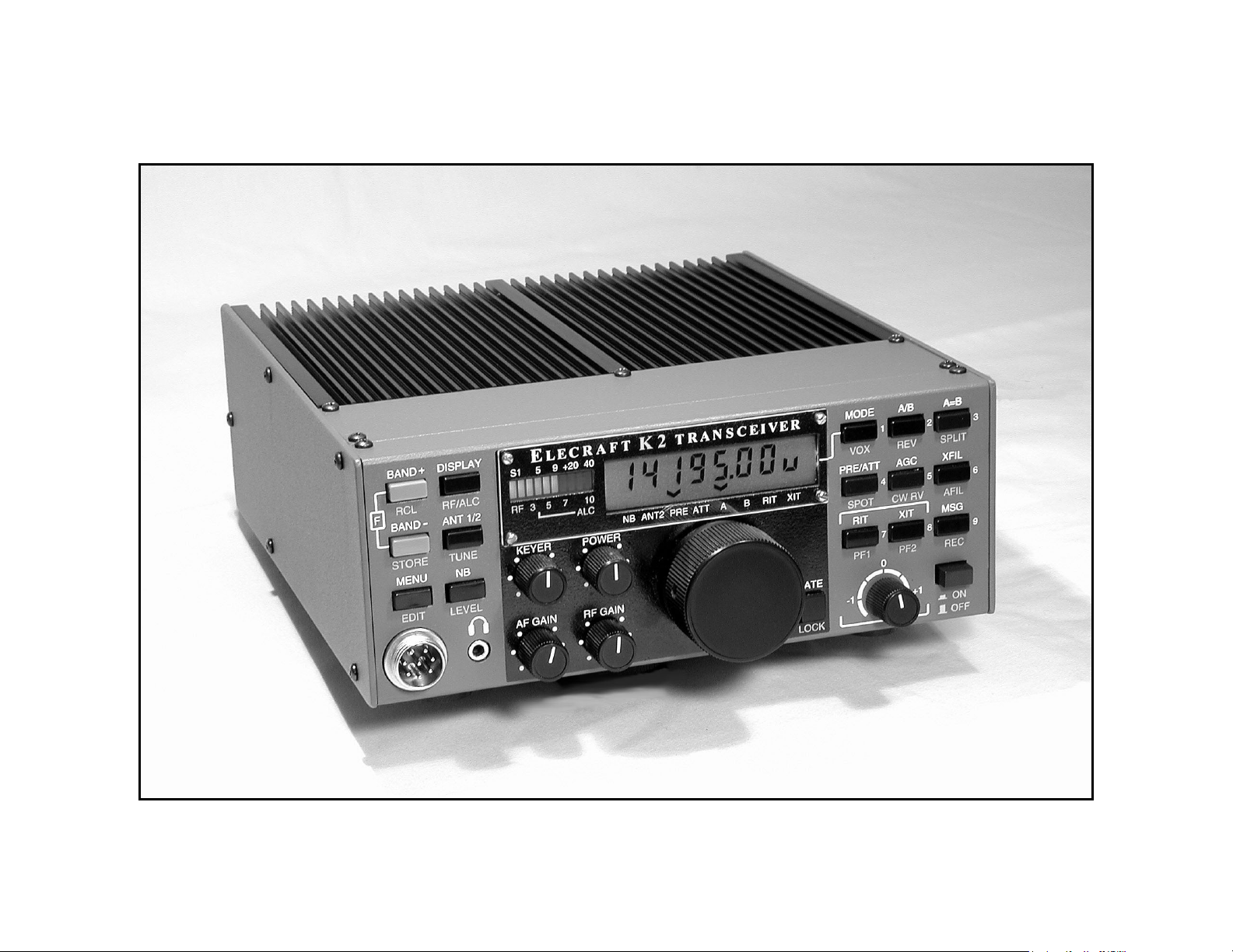
Appendix G, 100-W Stage and RS-232 I/O (K2/100)
Rev A, May 13, 2002
1
Page 2

Table of Contents
Introduction................................................................................................................................................................................................................3
Preparation for Assembly.................................................................................................................................................................................................3
Tools Required..............................................................................................................................................................................................................3
Pre-Wound Toroids........................................................................................................................................................................................................3
Parts Inventory...........................................................................................................................................................................................................3
Assembly, Part I......................................................................................................................................................................................................11
Initial Tests...............................................................................................................................................................................................................20
Assembly, Part II.....................................................................................................................................................................................................24
Alignment and Installation....................................................................................................................................................................................41
Receiver Tests.............................................................................................................................................................................................................44
SWR Bridge Null Adjustment (C1).................................................................................................................................................................................44
Power Calibration (R26 and R27)...................................................................................................................................................................................45
Temperature Calibration (CAL tPA)................................................................................................................................................................................45
KPA100 Power Supply Test..........................................................................................................................................................................................45
Fan Test.....................................................................................................................................................................................................................46
External Amplifier Keying Test (PA KEY).......................................................................................................................................................................46
Bias Current Adjustment...............................................................................................................................................................................................46
Transmit Tests.............................................................................................................................................................................................................47
Installation..................................................................................................................................................................................................................48
Using the K2/100 at High Power.........................................................................................................................................................................49
Power Supply..............................................................................................................................................................................................................49
Antenna......................................................................................................................................................................................................................49
Controls.....................................................................................................................................................................................................................50
Remote Control using the RS232 Port...............................................................................................................................................................51
Control Board Preparation.............................................................................................................................................................................................51
RS-232 Interface Setup and Test.....................................................................................................................................................................................52
Computer Control........................................................................................................................................................................................................53
K2/100 Specifications............................................................................................................................................................................................56
Troubleshooting and Repair................................................................................................................................................................................57
Circuit Details..........................................................................................................................................................................................................60
KPA100 Schematic.................................................................................................................................................................................................61
Parts Placement Drawing.....................................................................................................................................................................................63
2
Page 3
Introduction
Pre-Wound Toroids
Appendix G describes assembly of the K2/100 transceiver's internal
100-watt final output stage (KPA100 board). The PC board includes
two conservatively-rated RF power transistors, low-pass filters, SWR
bridge, monitoring circuits, speaker, and an RS232 interface. Filter
switching, T-R sequencing, and other configuration is handled by the
K2/100's main microcontroller.
KPA100 assembly and installation should be done only after the
transceiver has been aligned and tested at the 10-watt level.
Preparation for Assembly
With all equipment that operates at high power levels, proper
assembly and alignment are critical for safe and reliable operation.
Follow the instructions carefully and make all of the recommended
measurements. Do not substitute components or perform any assembly
steps out of order.
Please read the following information regarding tools and
toroids before proceeding.
Tools Required
The following tools are required to build this kit:
• Flush-cutters (Hakko CHP-170, Xcelite 170, etc.). Ordinary
diagonal cutters are not suitable for flush-cutting (trimming leads
very close to the board).
• Temperature-controlled soldering station with a fine-point,
800-degree (F) tip. Do not use a high-wattage iron or gun with
small components, since this can damage pads, traces, or the parts
themselves.
• Larger iron or soldering gun. This will be used only for
installation of power transistors, output transformer, and DC
power wiring. A low-wattage iron cannot be used for these steps.
• Digital Multimeter (DMM). A DMM with capacitance
measurement capability is desirable, though not required.
Refer to our web site for tool sources and solder recommendations.
The toroids on the KPA100 board are not difficult to wind, and
detailed instructions are provided (beginning on page 24). All toroids
must be wound and prepared correctly, or the power transistors
may be damaged.
If you prefer not to wind the toroids yourself, you can obtain a full set
of pre-wound toroids (with leads stripped and tinned) from an Elecraftqualified source. A toroid order form may have been supplied with your
kit. You can also find ordering information at www.elecraft.com. You
do not need to send your cores or wire to the winding service.
Parts Inventory
Set the heat sink and painted panels aside until needed. Leave
them wrapped to protect their finish.
You should do a complete inventory (parts list starts on page 4),
which will take 2 to 3 hours. If anything is missing, contact Elecraft.
Color codes and other markings are shown in parentheses. Refer to
Appendix A of the owner's manual for additional parts photos.
Some components in this kit can be damaged by static
discharge. Before handling diodes, transistors, and ICs, touch
a grounded, unpainted metal surface, or use a wrist strap.
Parts List Notes:
• LS = lead spacing (0.1" = 2.5 mm, 0.2" = 5 mm, 0.4" = 10 mm.)
• In some cases, two capacitor types will have the same value
but different voltage ratings or lead spacing (LS). To avoid
assembly errors, you must positively identify these
capacitors and keep them separate from each other. Use
your DMM to verify values if possible.
• Parts shown in bold are for use on the K2 RF or Control boards.
• Flat-head screws are measured from the top of the head; pan head
screws are measured from beneath the head.
3
Page 4
Picture Ref. Designator(s) QTY Description Part #
C5B 1 Cap., 18 pF ("18"), 5%, 500V or 1KV disc, 0.2" LS (may have black band) E530088
C3B,C4B 2 Cap., 27 pF ("27"), 5%, 500V or 1KV disc, 0.2" LS E530089
C5F 1 Cap., 33 pF ("33"), 5%, 500V or 1KV disc, 0.2" LS E530090
C3H 1 Cap., 39 pF ("39"), 5%, 500V or 1KV disc, 0.2" LS E530091
C5D 1 Cap., 47 pF ("47"), 5%, 500V or 1KV disc, 0.2" LS E530092
C4D 1 Cap., 56 pF ("56"), 5%, 500V or 1KV disc, 0.2" LS (may have black band) E530093
C5A,C6C 2 Cap., 68 pF ("68"), 5%, 500V or 1KV disc, 0.2" LS E530094
C3E,C5G 2 Cap., 82 pF ("82"), 5%, 500V or 1KV disc, 0.2" LS E530095
C4E 1 Cap., 120 pF ("121"), 5%, 500V or 1KV disc, 0.2" LS E530096
C3G,C4A,C5C,C5E,
C6E
C2B,C3C,C3J 3 Cap., 220 pF ("221"), 5%, 500V or 1KV disc, 0.2" LS E530098
C3A,C3D,C4C,C6F 4 Cap., 270 pF ("271"), 5%, 500V or 1KV disc, 0.2" LS E530099
C3F,C6A,C6B,C6G 4 Cap., 330 pF ("331"), 5%, 500V or 1KV disc, 0.2" LS E530100
C2D 1 Cap., 390 pF ("391"), 5%, 500V or 1KV disc, 0.2" LS E530101
C26 1 Cap., 33 pF ("33"), 5%, 50V disc, 0.2" LS (do not confuse with C5F) E530064
C41,C95 2 Cap., 100 pF ("101"), 5%, 200V disc, 0.2" LS E530034
C66 1 Cap., 180 pF ("181"), 5%, 50V disc, 0.2" LS; voltage may not be marked E530008
C80,C81 2 Cap., 4700 pF ("472"), 10%, 100V disc, 0.25" LS E530102
C2E,C83 alternate 2 Cap., 1000 pF ("1000"), 5%, 500V silver mica E530085
C2A,C6D,C83 3 Cap., 1200 pF ("1200"), 5%, 500V silver mica E530033
C2C 1 Cap., 2200 pF ("2200"), 5%, 500V silver mica E530086
C84 1 Cap., .001 µF ("102"), 5%, 50V mono, 0.1" LS E530074
C25,C69,C70,C87,
C88, CTRL-Ctxd
C82 1 Cap., 1200 pF ("122"), 5%, 50V mono 0.2" LS E530005
C71 1 Cap., .0018 µF ("182"), 5%, 200V mono, 0.2" LS E530104
C64 1 Cap., .0018 µF ("182"), 5%, 630V mono, 0.4" LS E530105
C7,C8,C9,C12–C22,
C24,C28,C29,C32,
C50,C65,C72,C73,
C74,C76,C97–C99
C37,C38,C39,C44,
C46,C68,C89,C90
C36,C42,C43,C77 4 Cap., .015 µF ("153" or "15N"), 5%, 250V mono, 0.2" LS E530082
C31,C67 2 Cap., .033 µF ("333" or "33N"), 5%, 250V mono, 0.2" LS E530083
C79 1 Cap., .039 µF ("393"), 5%, 200V mono, 0.4" LS E530103
5 Cap., 150 pF ("151"), 5%, 500V or 1KV disc, 0.2" LS E530097
6 Cap., .001 µF ("102"), 5%, 50V mono, 0.2" LS
(CTRL-Ctxd may be needed for K2 Control board; see text)
27 Cap., .01 µF ("103"), 5%, 50V mono, 0.1" LS E530019
8 Cap., .01 µF ("103"), 5%, 50V mono, 0.2" LS E530009
E530001
4
Page 5
Picture Ref. Designator(s) QTY Description Part #
C48,C49,C52–C57,
C61-C63,C85,C86.
RF-Crf
C30,C33,C34,C75 4 Cap., 0.1 µF ("104"), 20%, 50V mono, 0.1" LS E530020
C10,C11,C23,C35,
C58,C59,C40,
CTRL-C42
C1,C27 2 Cap., 5-30 pF ceramic trimmer E540001
C60 1 Cap., 100 µF, 16V electrolytic E530061
C51 1 Cap., 470 µF, 25V electrolytic E530084
D1-D8 8 Diode, 1N4148 E560002
D9 1 Diode, SB530 E560003
D10,D13 2 Diode, 1N5404 E560010
D11,D12,D14 3 Diode, 1N4007 E560001
D16,D17 2 Diode, 1N5711 E560004
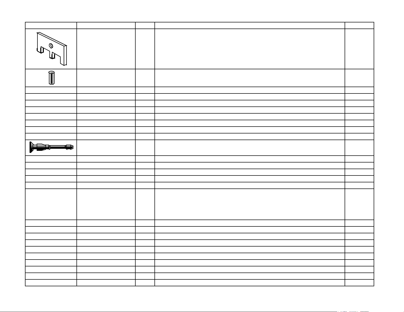
E1 1 Ground terminal, right angle PCB mount, 6-32 threaded E700012
FAN1 1 Fan, 12 V E980046
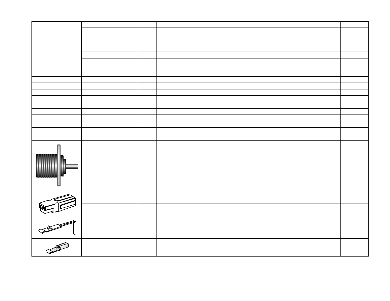
J2 1 Connector, SO239 (Antenna) E620064
Cap., .047 µF ("473"), 5%, 50V mono, 0.2" LS
14
(RF-Crf may be needed for the K2 RF board; see text)
8 Cap., 0.1 µF ("104"), 5%, 50V mono, 0.2" LS
(CTRL-C42 may be needed for the K2 Control board; see text)
E530025
E530011
J3, P3 2 Connector, DC power, red housing (13.8 VDC input and mating conn., +) E620059
J3, P3 2 Connector, DC power, black housing (13.8 VDC input and mating conn., -) E620060
MISC 2 PCB pin for J3, 25 amp right angle E620061
MISC 2 Crimp/solder terminal for P3, 30 amps E620062
5
Page 6
Picture Ref. Designator(s) QTY Description Part #
HDWR 2 Mounting plate for J3 E620063
MISC 1 Spring pin, 3/32" x 1/4" (2.4 x 6.4 mm); stabilizing pin for P3 E700071
J1,J4 2 Connector, 2p female housing, 0.156" spacing (12V and RF connectors) E620013
RF-P3, RF-P6 2 Mating connectors for J1 and J4, 2p male, 0.156" spacing (K2 RF board) E620012
HDWR 5 Crimp/solder terminal for J1 and J4, gold color (1 spare) E620014
J5 1 Connector, 2p female housing, 0.1" spacing (AF In) E620021
HDWR 3 Crimp/solder terminal for J5 (1 spare) E620022
J6 1 Connector, 1/8" mono jack w/switch, PCB mount (ext. speaker) E620056
J7 1 Connector, RCA jack, PCB mount (ext. PA key) E620057
J8 1 Connector, DB9F, PCB mount (RS232 interface) E620058
MISC 2 Keying insert for ribbon cable connector
(Shown approx. 4x actual size; may include large break-away tab)
MISC 1 Connector, DB9M (serial I/O cable, K2 end) E620049
MISC 1 Connector, DB9F (serial I/O cable, PC end) E620048
MISC 2 Backshell for serial I/O cable E620050
K1-K12 12 Relay, SPDT, 12 V E640011
L1,L2,L13,L14 4 Toroidal inductor, T50-2 core (iron powder, red, 0.5" dia.) E680005
L4-L8,L10-L12 8 Toroidal inductor, T50-10 core (iron powder, black, 0.5" dia.)
E700065
E680016
Note: One gray ferrite core of the same size is also supplied (see T4).
The T50-10 iron power cores have a shiny, black finish, while the
ferrite core is dull gray in color. Keep the two types separated.
L15,L16,L18 3 Toroidal inductor, T44-2 core (iron powder, red, 0.44" dia.) E680012
P1 1 Connector, 10 pin dual row (5 x 2), 0.1" spacing E620040
Q1,Q2 1 Matched set of (2) 2SC2879 transistors E850123
Q3,Q4 2 Transistor, NPN, MJE182, TO-225AA package E580016
Q5,Q8 2 Transistor, NPN, 2N3904, TO-92 E580017
Q6,Q7 2 Transistor, MOSFET, 200 V, ZVN4424, TO-92 E580005
Q10,Q11,Q12 3 Transistor, MOSFET, 60 V, 2N7000, TO-92 E580002
Q9 1 Transistor, HEXFET, 500 V, IRF830 or IRL620, TO-220 (tab may be cut) E580018
R2,R3 2 Resistor, 2.7 ohms, 5%, 1/4 W (RED-VIO-GOLD) E500055
R9 1 Resistor, 10 ohms, 5%, 1/4 W (BRN-BLK-BLK) E500054
6
Page 7
Picture Ref. Designator(s) QTY Description Part #
R10 1 Resistor, 47, 5%, 1/4 W (YEL-VIO-BLK) E500019
R1,R29,R15,R16 4 Resistor, 3.3 k, 5%, 1/4 W (ORG-ORG-RED) E500017
R8 1 Resistor, 10 k, 5%, 1/4 W (BRN-BLK-ORG) E500015
R5 1 Resistor, 15 k, 5%, 1/4 W (BRN-GRN-ORG) E500060
R4 1 Resistor, 100 k, 5%, 1/4W (BRN-BLK-YEL) E500006
R12 1 Resistor, 180 k, 5%, 1/4W (BRN-GRY-YEL) E500068
R11 1 Resistor, 510 k, 5%, 1/4W (GRN-BRN-YEL) E500069
R32 1 Resistor, 100 ohms, 1%, 1/4W (BRN-BLK-BLK-BLK)
Note: This resistor looks very similar to the small 100-µH RF choke
(RFC3, etc.). RF chokes can be identified by their much lower resistance,
if necessary (typically 1 to 8 ohms).
R30 1 Resistor, 3.09 k, 1%, 1/4W (ORG-BLK-WHT-BRN) E500072
R24,R25 2 Resistor, 8.45 k, 1%, 1/4W (GRY-YEL-GRN-BRN) E500071
R28,R31 2 Resistor, 200 ohms, 5%, 1W (RED-BLK-BRN) E500074
R23 1 Resistor, 10 ohms, 5%, 1 W (BRN-BLK-BLK) E500083
R14 1 Resistor, 470 ohms, 5%, 1W (YEL-VIO-BRN) E500075
R19,R20 2 Resistor, 3.6 ohms, 5%, 2W E500084
R21,R34,R35 3 Resistor, 10 ohms, 5%, 2W (do not confuse with R23) E500077
R38,R39 2 Resistor, 68 ohms, 5%, 2W E500078
R13,R22 2 Resistor, 100 ohms, 5%, 3W E500080
R7 1 Resistor, .005 ohms, 1%, 3W (current sensing) E500079
R6 1 Potentiometer, 1K trimmer ("102"), bias set E520010
R26,R27 2 Potentiometer, 100K trimmer ("104"), SWR set E520001
RFC1,RFC10 2 RF Choke, 100 µH ("101"), black body, 0.75" LS E690017
RFC3-RFC5,RFC11 4 RF Choke, 100 µH (BRN-BLK-BRN), tan body, 0.4" LS E690016
RFC6,RFC7,RFC8 3 RF Choke, 100 µH, miniature (BRN-BLK-BRN), tan body, 0.2" LS E690013
RFC9 1 RF Choke, 15 µH, miniature (BRN-GRN-BLK), tan body, 0.2" LS E690012
RP1 1 Resistor network, 3.9 k, 8 pins (marked part number should include "392") E510000
SP1 1 Speaker, 4 ohms, 3W E980007
T1 1 Transformer, small binocular toroid core (gray, approx. 0.5" x 0.75") E680014
E500059
T2 1 Transformer, large binocular toroid core (gray, approx. 1" x 1.2") E680015
T3 1 Transformer, FT37-61 toroidal core (gray, 0.37" dia.) E680002
7
Page 8
Picture Ref. Designator(s) QTY Description Part #
T4 1 Transformer, FT50-43 toroidal core (gray, 0.5" dia.) E680008
U1 1 IC, PIC16F872 microcontroller, pre-programmed, KPA100 E610011
MISC 1 Socket for U1, 28 pins E620011
U2 1 IC, octal peripheral driver, TD62083AP (alt: ULN2803) E600040
U3 1 IC, 5-volt regulator, 78L05 E600029
U4 1 IC, RS-232 driver/receiver, MAX1406CPE (alt: LT1039CN16) E600036
U5 1 IC, dual op-amp, LM358AN E600010
U6 1 IC, high-current op-amp w/enable, EL5146CN E600041
U7 1 IC, dual op-amp, rail-to-rail, LMC6482AIN E600011
X1 1 Crystal, 16.289MHz, low profile ("S162ECSL") E660014
X2 1 Crystal, 4 MHz ("4.00-20") E660006
Z1 2 Ferrite beads, 0.23" (6 mm) long; two beads on a 1N4007 diode lead) E980029
HDWR 2 Fuse holder housing, twist-lock (for external 20A fuse) E980047
HDWR 2 Fuse holder contacts, #12 size E980048
HDWR 1 Fuse holder spring, for 1.25" long fuse E980049
HDWR 2 Fuse, 20A, Littlefuse #312020 or equivalent (1 spare) E980050
HDWR 2 Standoff, M-F, 3/16 dia. x 3/16" long hex 4-40 thd (for J8) E700052
HDWR 5 Standoff, 3/16 dia. x 3/16" long hex 4-40 thd (between PCB and heat sink) E700068
HDWR 2 Standoff, 3/16 dia. x 1/2" long hex 4-40 thd (between PCB and shield) E700061
HDWR 5 Standoff, 3/16 dia. x 5/8" long hex 4-40 thd (between PCB and shield) E700060
HDWR 14 Screw, 4-40 x 3/16" pan head, black anodized (2 spares) E700015
HDWR 5 Screw, 4-40 x 3/16" undercut flathead, black anodized (1 spare) E700025
HDWR 19 Screw, 4-40 x 1/4" panhead (2 spares) E700005
HDWR 3 Screw, 4-40 x 1/4" flathead (1 spare) E700063
HDWR 5 Screw, 4-40 x 9/16" undercut flathead (1 spare) E700064
HDWR 8 Set screw, 4-40 x 1/2", .05" hex socket head, stainless steel (1 spare) E700066
HDWR 12 Nut, 4-40 small pattern (2 spares) E700055
HDWR 1 Nut, 6-32 hex, stainless steel (for GND screw) E700069
HDWR 33 Lock washer, #4 split (3 spares) E700004
HDWR 2 Flat washer, #6, Stainless Steel E700067
HDWR 1 Solder lug (used for grounding J2) E700062
8
Page 9
Picture Ref. Designator(s) QTY Description Part #
HDWR 1 Thumbscrew, 6-32 x 1/2", black plastic knob (for GND screw, E1) E700070
HDWR 5 Fibre washer for speaker, #4, .047" thick x 0.25" dia. (1 spare) E700028
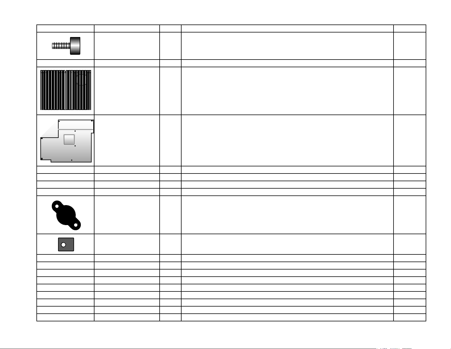
MISC 1 Heat sink, KPA100, approx. 7.6" W x 6" L (19.23 x 15.2 cm) E100127
MISC 1 Shield, KPA100, approx. 7.3" W x 6" L (18.5 x 15.2 cm) E100137
MISC 1 PC board, KPA100 E100134
MISC 1 Top cover trim panel, KPA100, painted (wrapped in paper) E100135
MISC 1 Rear panel, KPA100, painted and silk-screened (wrapped in paper) E100136
MISC 1 Grille cloth, black, approx. 3 x 3" (7.5 x 7.5 cm) E980053
MISC 2 Thermal pad for flange-mount power transistor (Q1 and Q2) E980051
MISC 2 TO-126 thermal pad, self-adhesive (Q3, Q4) E980052
MISC 1 BNC connector cap, plastic (to cap K2's BNC antenna jack) E980006
MISC 26 ft. Enamel wire, #22 red (for all lowpass filter toroids and L18) E760018
MISC 9 ft. Enamel wire, #26 red (for T3, T4, L15, L16) E760002
MISC 3 ft. Enamel wire, #26 green (for T3 and T4) E760004
MISC 5 ft. 2-conductor wire, #12 stranded, red/black (for DC power wiring) E760017
MISC 1 ft. RG174 coax (for RF cable to K2 RF board) E760010
MISC 1 10-conductor ribbon cable with pre-installed connectors; 4" long E980045
MISC 1 ft. 2-conductor speaker cable, #24 stranded (for J5 and speaker) E760012
MISC 10 ft. 4-conductor shielded cable (serial I/O cable) E760009
9
Page 10
Picture Ref. Designator(s) QTY Description Part #
MISC 1 ft. Stranded insulated hookup wire, #20 black (for DC cable to K2 RF board) E760006
MISC 1 ft. Stranded insulated hookup wire, #20 red (for DC cable to K2 RF board) E760007
MISC 1 ft. Hookup wire, #24, solid conductor, green ins. (for K2 Control board mod) E760008
MISC 1 ft. Stranded, Teflon-insulated wire, #22 gray (for T1) E760020
MISC 2 ft. Stranded, Teflon-insulated wire, #18 gray (for T2) E760021
MISC 3 Cable tie, 3" E980002
MISC 1 Allen wrench, .05", short handled (for 1/2" heat sink set screws) E980008
MISC 1 Sand paper, 180-grit (for heat sink preparation) E980055
10
Page 11
Assembly, Part I
Downloaded by
RadioAmateur.EU
Place the KPA100 PC board as shown in Figure 1, and identify
the top side, which has most of the components. (A complete parts
placement drawing can be found at the end of this appendix.) The
"Front Edge" and "Back Edge" designations are based on the board's
orientation when installed in the K2.
With the bottom side of the board facing you (speaker cutout at
the upper right), locate the position for resistor R28, along the back
edge, far right. The label "R28" is just above of the resistor’s outline.
Install a 200-ohm, 1-watt resistor (red-black-brown) at R28.
Form the leads to fit the given pad spacing. Bend the leads to hold the
resistor in place. Note: It's a good idea to orient all resistors in one
direction for ease in reading the color codes later. Orient R28 with its
first color band (red) toward the left.
Back Edge
KPA100 REV A
(Top Side)
J7
Figure 1
J3
Front Edge
J6
J8
Make sure R28 is seated flat on the board, with no excess lead
length exposed. This is necessary to keep the resistor from touching
the heat sink, which will be attached later.
Solder R28 from the top side of the board. Do not use an
excessive amount of solder. Trim the leads to about 1/16" (1.5 mm) or
shorter.
i
If your solder joints are not clean and shiny, your iron
may not be hot enough, or you may be using the wrong type of
solder. These "cold" solder joints will likely result in poor
performance, reliability problems, or component failure.
Before proceeding, consult our web site for additional
soldering instructions and tool recommendations.
11
Page 12
On the top side of the board, locate the component outline for
.005-ohm current-sensing resistor R7 (near the DC power connector,
J3). Each of R7's pads has three holes.
i
The leads on small capacitors are fragile. Do not pull
on the leads or bend them excessively.
Bend the leads of the .005-ohm, 3-watt resistor to match the
spacing between R7s innermost pair of holes (see Figure 2a). Install the
resistor, pressing it down onto the board as far as it will go.
On the bottom side, fold R7's leads outward so they lay flat
against the pads (Figure 2b). Trim the leads to match the size of the
pads. Solder each lead over the full length of the pad.
Note: Components may be soldered one at a time or in groups. Leads
can be trimmed either before or after soldering. Flush trimming
(trimming very close to the board) is required only when specified.
Otherwise, trim leads to about 1/16" [1.5 mm] or less in length.
(a)
(b)
Sort all capacitors into groups by capacitance value. Start by
grouping them by physical appearance (size, color, etc.).
In all cases where two or more capacitor types have the same
value, further sort them by lead spacing and voltage rating. The parts
list provides identification details for specific capacitor types.
Locate an 0.1- µF ("104") capacitor with 0.1" lead spacing for
use at C75.
Install C75 at its indicated location on the bottom of the board,
near the back edge. The capacitor must be seated as close to the board
as possible, with 1/16" (3 mm) or less lead length exposed. Remove
any U-shaped bends or folds using long-nose pliers. Solder C75 from
the top side of the board.
Install a .01-µF ("103") capacitor with 0.1" lead spacing at
C65. C65 is located on the bottom side of the board, near the front
edge. Keep the lead length short, as described in the previous step.
Figure 2
12
Page 13
The color bands on 1/4-watt 1% resistors can be difficult to read.
Use a DMM (digital multimeter) to verify the values of all these
resistors. Tape them to a piece of paper with their values labeled.
Install the resistors listed below on the top side of the board. Start
with R3, which is at the front edge of the board, near the "KPA100"
label.
In general, assembly proceeds from left to right and from front edge to
back edge on the PC board.
__ R3, 2.7 ohms, 1/4 W (red-violet-gold)
__ R24 and __ R25, 8.45 k, 1%, 1/4 W (gray-yellow-green-brown)
__ R15 and __ R16, 3.3 k, 1/4 W (orange-orange-red)
__ R31, 200 ohms, 1 W (red-black-brown)
__ R4, 100 k, 1/4 W (brown-black-yellow)
__ R10, 47 ohms, 1/4 W (yellow-violet-black)
__ R5, 15 k, 1/4 W (brown-green-orange)
__ R8, 10 k, 1/4 W (brown-black-orange)
__ R30, 3.09 k, 1% (orange-black-white-brown)
__ R32, 100 ohms, 1%, 1/4 W (brown-black-black-black)
__ R14, 470 ohms, 1 W (YEL-VIO-BRN) (located near back edge)
__ R11, 510 k, 1/4 W (green-brown-yellow)
__ R12, 180 k, 1/4 W (brown-gray-yellow)
__ R13, 100 ohms, 3 watts
__ R1, 3.3 k, 1/4 W (orange-orange-red)
__ R2, 2.7 ohms, 1/4 W (red-violet-gold)
__ R29, 3.3 k, 1/4 W (orange-orange-red), location: far left, near small notch
Install RFC11 on the bottom side of the board. Its location is
close to the cutout for power transistor Q1.
Make sure RFC11 is pressed against the board as far as it will go,
then solder it from the top side of the board.
Install and solder the RF chokes listed below. Limit soldering time
on miniature chokes (2 to 3 seconds per lead). All chokes are on the
top side of the board near connectors J3 and J8.
__ RFC9, 15 µH, miniature (brown-green-black)
__ RFC6, __ RFC7, __ RFC8, 100 µH, miniature (brown-black-brown)
__ RFC3, __ RFC4, __ RFC5, 100 µH, small (brown-black-brown)
__ RFC1, 100 µH (101), large
Check the resistance across each RF choke using the lowest
resistance scale of your DMM. This will ensure that the chokes were
not damaged during soldering. All readings should be under 10 ohms.
Sort all of the diodes according to type. Use a magnifying glass if
necessary to positively identify glass diodes (1N4148 and 1N5711).
Install diodes D1-D8 (1N4148) on the bottom side of the board,
near the large cutout, but do not solder yet. Bend the leads very close
to the body to fit the given pad spacing. The banded end of each diode
(cathode) must be aligned with the band on its component outline.
Make sure D1-D8 are seated as far down on the PC board as
possible. Solder and trim the leads.
Sort all of the RF chokes by size and value. Do not pull on the
leads, which are fragile and can be easily damaged.
Locate a small 100-µH RF choke for use at RFC11 (tan body,
BRN-BLK-BRN color code, 0.4" lead spacing). Do not use one of the
miniature 100-µH RF chokes, which has a much smaller lead spacing.
13
Page 14
Install the remaining diodes on the top side of the board. Start
with D17, at the lower left-hand corner near the small notch.
__ D17, 1N5711 __ D16, 1N5711
__ D10, 1N5404 __ D13, 1N5404
Use a ruler to check the height of all capacitors just installed, as
well as C65 (near the front edge) and C75 (near the back edge). If any
capacitor body extends to 3/16" (4.5 mm) or more above the surface
of the board, fold it down toward the board. The capacitors should not
touch any adjacent pads.
Note: D14, 12, and 11 are not all oriented in the same direction
__ D14, 1N4007 __ D12, 1N4007 __ D11, 1N4007
(Save the 1N4007 leads for use as jumpers, etc., in later steps)
__ D9, SB530
Using the diode check scale on your DMM, test all of the diodes
on the board. (This will ensure that diodes have not been damaged
during installation.) First, touch the red (+) lead of the DMM to the
anode (non-banded end), and the black (-) lead to the cathode (banded
end); the meter should indicate a forward voltage in the range of 0.1 to
0.7 volts, varying with diode type. Next, reverse the leads; the DMM
should show an open-circuit indication (flashing "3.000" or "0.000,"
etc.).
Near the "ELECRAFT" label, you’ll find a short jumper location,
identified by a ground symbol ( ). Use a discarded 1N4007 diode lead
to make a 3/4" (19 mm) U-shaped wire for this jumper. Mount the
jumper on the top side of the board, with the top of the U-shape
approx. 1/4" (6 mm) above the board. Solder it from the bottom side.
Install the following capacitors on the bottom side of the PC
board, but do not solder yet. Capacitors must be seated as close to the
board as possible. About 1/16" (3 mm) of lead length may remain
exposed. Remove any U-shaped bends or folds using long-nose pliers.
Note: These capacitors are all .01 µF (103), with 0.1" lead spacing.
Solder the capacitors from the top side. Use just enough solder
to fill the hole, since the leads will be flush-trimmed in the
next step.
i
Important: Relays K1-K12 will be installed on the top side of
the board, opposite capacitors C13-C22 and C29. This requires that
the capacitor leads and their surrounding solder filets be trimmed as
close to the PC board as possible.
Flush-trim the leads of C13-C22 and C29 on the top side of the
board. After trimming, the leads and surrounding solder filets should be
no more than 1/32" (0.8 mm) high.
Install the 0.2" lead spacing capacitors listed below on the top
side of the board. Start with C11, which is along the front edge of the
board near the "KPA100" label.
__ C11, 0.1 µF (104) __ C23, 0.1 µF (104) __ C25, .001 µF (102)
__ C68, .01 µF (103) __ C89, .01 µF (103)
__ C26, 33 pF, 50V (Do not confuse with C5F, rated at 500 V or 1 KV)
__ C41, 100 pF (101)
__ C38, .01 µF (103) __ C39, .01 µF (103)
__ C37, .01 µF (103) __ C36, 0.015 µF (153, 15N)
__ C35, 0.1 µF (104) __ C44, .01 µF (103)
__ C42, 0.015 µF (153, 15N) __ C43, 0.015 µF (153, 15N)
__ C46, .01 µF (103) __ C40, 0.1 µF (104)
__ C99 ⇒ __ C97 ⇒ __ C98 ⇒ __ C22
__ C74 __ C29 __ C13 __ C15
__ C17 __ C19 __ C21 __ C14
__ C16 __ C18 __ C20
14
Page 15

Place relays at locations K1-K12, excluding K3. (K3 will be
installed after the output transformer, T2.) Each relay can only be
installed one way; the white mark on the relay must be oriented as
indicated by the mark on the component outline. Do not solder the
relays yet, and do not clip or bend the relay leads.
Inspect each relay to make sure that it is seated flat against the
board. If not, remove it and flush-trim the leads which are preventing
it from sitting flat against the board.
Make sure that you have not installed relay K3.
Using a book or other flat object to hold the relays in place on
the top side of the board, flip the board over. Solder two diagonal
corner pins on each relay.
Inspect the 11 relays closely to make sure that they’re seated flat
against the PC board. If not, re-heat the corner pins one a time while
pressing down on the relay. Once all relays are properly seated, solder
the remaining pins. Do not trim relay leads, which can cause
mechanical stress, reducing the life of the relay.
Install the small capacitors listed below. (The first capacitor in
the list, C50, is near trimmer C27). Lead spacing (LS) and voltage
are shown where required to identify the capacitor type.
__ C50, .01 µF (103), 0.1" LS __ C30, 0.1 µF (104), 0.1" LS
__ C33, 0.1 µF (104), 0.1" LS __ C34, 0.1 µF (104), 0.1" LS
__ C61, .047 µF (473) __ C62, .047 µF (473)
__ C63, .047 µF (473) __ C70, .001 µF (102), 0.2" LS
__ C69, .001 µF (102), 0.2" LS __ C55, .047 µF (473)
__ C56, .047 µF (473) __ C57, .047 µF (473)
__ C54, .047 µF (473) __ C53, .047 µF (473)
__ C52, .047 µF (473) __ C49, .047 µF (473)
__ C48, .047 µF (473) __ C31, .033 µF (333, 33N)
__ C86, .047 µF (473) __ C76, .01 µF (103), 0.1" LS
__ C67, .033 µF (333, 33N) __ C77, .015 µF (153, 15N)
__ C82, 1200 pF (122), 50V (do not confuse with 1200 pF, 500-V mica)
__ C66, 180 pF (181)
__ C28 .01 µF (103), 0.1" LS (far left side of the board near K4)
__ C12, .01 µF (103), 0.1" LS
Install resistor network RP1 near the "KPA100" label at the
front edge of the board. The dotted (pin 1) end of RP1 should be
oriented to the left. (RP1 is symmetrical and can be reversed, but this
orientation will help visually identify the pin 1 end.)
Install trimmer potentiometers R26 and R27 (100 k, "104") near
the speaker cutout. The trimmers will sit a small distance above the PC
board on the pin shoulders. Set the trimmers to their midpoints.
Install trimmer potentiometer R6 (1 k, "102") at the right side of
the board near T1. Set the trimmer fully counter-clockwise.
Install the 5 to 30 pF ceramic trimmer capacitors, C1 and C27.
C1 is at the far left near the small notch. C27 is near the
microcontroller, U1 (16F872). Orient the flat side of each trimmer as
indicated.
Using a small flat-blade screwdriver, set both trimmers to their
midpoints (screwdriver slot perpendicular to the flat side).
__ C95, 100 pF (101) (near small notch and T4)
__ C88, .001 µF (102), 0.2" LS __ C87, .001 µF (102), 0.2" LS
__ C24, .01 µF (103), 0.1" LS __ C85, .047 µF (473)
__ C90, .01 µF (103), 0.2" LS __ C71, .0018 µF (182), 0.2" LS
__ C72, .01 µF (103), 0.1" LS __ C73, .01 µF (103), 0.1" LS
__ C10, 0.1 µF (104), 0.2" LS __ C32, .01 µF (103), 0.1" LS
__ C7, .01 µF (103), 0.1" LS __ C8, .01 µF (103), 0.1" LS
__ C9, .01 µF (103), 0.1" LS __ C84, .001 µF (102), 0.1" LS
15
Page 16
Install the low-pass filter capacitors listed below. All are 500 V or
1KV (1000 V) disc, with 0.2" lead spacing. These capacitors are
located on the left side of the board between the two rows of relays
(K3-K12).
Note: Some of these capacitors are arranged in close-spaced groups of
three on the board. Look at all of the reference designators in a
group to be sure you know which capacitors they refer to.
__ C5B, 18 pF (may have black band on top and no marked voltage)
__ C3B, and __ C4B, 27 pF
__ C5F, 33 pF (Do not confuse with C26, which is 33 pF, 50 volts)
__ C3H, 39 pF
__ C5D, 47 pF
__ C4D, 56 pF (may have black band on top and no marked voltage)
__ C5A, 68 pF
__ C6C, 68 pF (note: C6D pertains to the large cap to the left of C6C)
__ C3E, and __ C5G, 82 pF
__ C4E, 120 pF (121)
__ C3G, __ C4A, __ C5C, __ C5E, and __ C6E, 150 pF (151)
__ C2B, __ C3C, and __ C3J, 220 pF (221)
__ C3A, __ C3D, __ C4C, and __ C6F, 270 pF (271)
__ C3F, __ C6A, __ C6B, and __ C6G, 330 pF (331)
__ C2D, 390 pF (391)
Install the 4 MHz crystal (X2) near the microcontroller (U1).
X2 must be seated flat against the board, with no insulators or
other spacers, or the metal shield will not fit correctly.
Cut two 3/4" (19 mm) bare wires (use small component leads).
Insert a bare wire into the grounding hole provided just to the left
of X2. Solder this wire to the side of the crystal can, not the
top, or it will prevent installation of the shield in a later step.
Keep soldering time below 5 seconds; if it takes longer, your iron may
not be hot enough, or your iron tip may not be making good contact
with the crystal can.
Turn the board over, then solder and trim X2's ground wire.
Ground crystal X1 using the second bare wire. X1 is low profile, so
the wire can be soldered to the top of the can. Avoid overheating.
Install the 10-pin, dual-row (5x2) male connector at P1, but do
not solder yet. Figure 3 shows P1 as viewed from right side of the
board. The plastic part of the connector must be on the top side of the
board, with the long end of the pins pointed up. The short ends are
inserted into the board.
Install the .039 µF capacitor, C79 (0.4" lead spacing, "393" or
".039 µF" label). C79 is located near relay K2.
Install a .0018 µF ("182") capacitor with 0.4" lead spacing at
C64. C64 is located near relay K2.
Install the electrolytic capacitors, C51 and C60. C51 (470 µF) is
near the large transformer, T2. C60 (100 µF) is near T1. The (+) lead
must be installed in the hole marked with a "+". The (+) lead is usually
longer than the (–) lead, and the (–) lead is identified by a black or
white stripe.
Install the low-profile 16.289 MHz crystal ("S162ECSL") at X1,
near the speaker cutout. Make sure the crystal is seated flat against the
board, then solder. Use a minimum amount of solder to avoid a short
under the can. Note: Insulators are not needed for crystals. The solder
mask on the top of the board provides adequate insulation.
P1
Figure 3
Solder just one pin of P1, from the bottom side. Note: P1's plastic
body can melt if too much heat is applied, causing the pins to be mispositioned. Limit soldering time to 2 to 3 seconds.
Examine the placement of P1. If it is not flat against the board,
re-heat the soldered pin while pressing down on the connector.
Once P1 is in the right position, solder the remaining pins. Do not
trim the leads.
16
Page 17
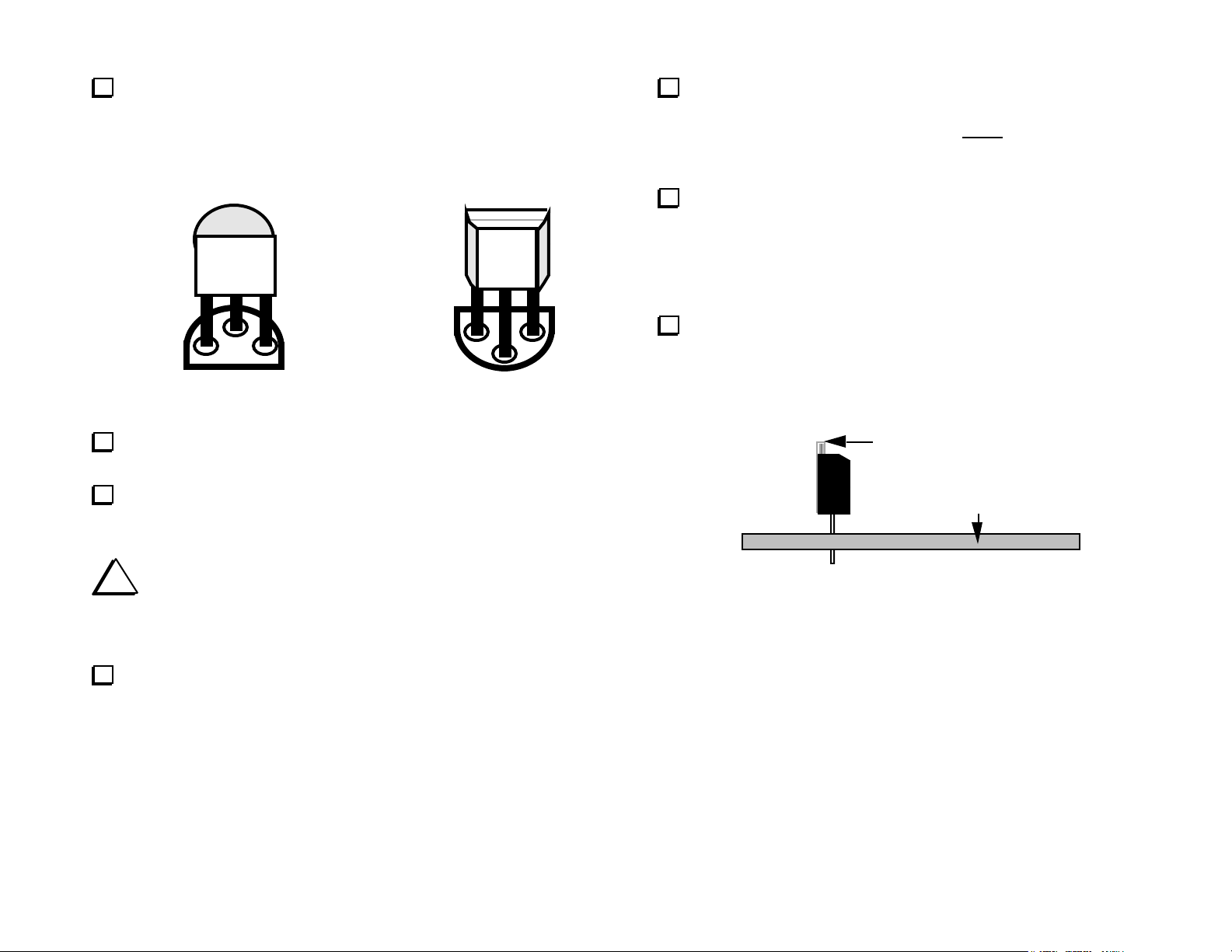
Install a 2N3904 transistor at Q8, near X1. (Use a magnifying
glass if necessary to identify TO-92 package transistors.) The flat side
of the transistor must be oriented toward the flat side of its outline as
shown in Figure 4a.
ZVN
(a)
(b)
Figure 4
4424A
MOSFET transistors Q6 and Q7 (ZVN4424) have a modified
TO-92 package that must be oriented as shown in Figure 4b. The
labeled side of these transistors faces away from the flat side
of the outline. Install and solder Q6 and Q7, which are located
between relays K1 and K2.
Q9 is a TO-220 package MOSFET (IRF830 or IRL620) with a
metal tab. The tab may have been cut off already. If not, you'll need to
trim it. Using heavy wire cutters or tin snips, cut off most of the tab
(see Figure 5). This is necessary to prevent the tab from shorting to
the shield in later steps. Do not use flush cutters or other small
cutting tools to cut off the tab; this may damage the tool.
Install Q9 vertically as shown below. The transistor will sit above
the board due to the shoulders on the leads. The tab must be
oriented toward J7 as indicated by the component outline. Trim
the pins on the bottom after soldering.
Install another 2N3904 at Q5, which is on the right side of the
board near potentiometer R6 (labeled "BIAS SET").
Install voltage regulator U3 (78L05), which has a 3-lead TO-92
package like the 2N3904 transistor. U3 is located in the right-front
corner of the board near connector P1.
i
The MOSFET transistors to be installed in the following
steps can be easily damaged by static discharge. Before and
during installation of these devices, touch an unpainted,
grounded metal surface.
Install MOSFET transistors Q10, Q11, Q12 (2N7000), which are
located near the "KPA100" label. The flat side of each transistor must
be aligned with the flat side of its outline as shown in Figure 4a.
Shortened Tab
Back edge of PCB
Figure 5
17
Page 18
Transistor Q3 (MJE182) will be installed on the bottom side of
the board, near the board cutout for power transistor Q2. Place the
transistor over its outline, with the metal side of the package
facing away from the board. Bend the three leads at right angles to
match the given pad locations, but do not solder yet. Note: the leads
will break if bent too many times.
Bend two opposite corner pins on the bottom side to hold the IC
in place. Solder all 8 pins (about 1 to 2 seconds per pin).
Install the ICs listed below. All are located to the right of U5.
Compare the part number on the IC to the number printed on the
board, and make sure that the pin 1 end is oriented correctly.
Insert Q3's leads into their holes. Center the transistor's plastic
body within its component outline. Re-form the leads if necessary.
Verify that Q3's metal side is facing away from the board, then
solder the leads from the top side, keeping the transistor pressed down
against the board.
Install Q4 in the same manner.
i
Before handling ICs, touch a metal surface. ICs
damaged by electrostatic discharge can become intermittent,
and the resulting problems may be difficult to troubleshoot.
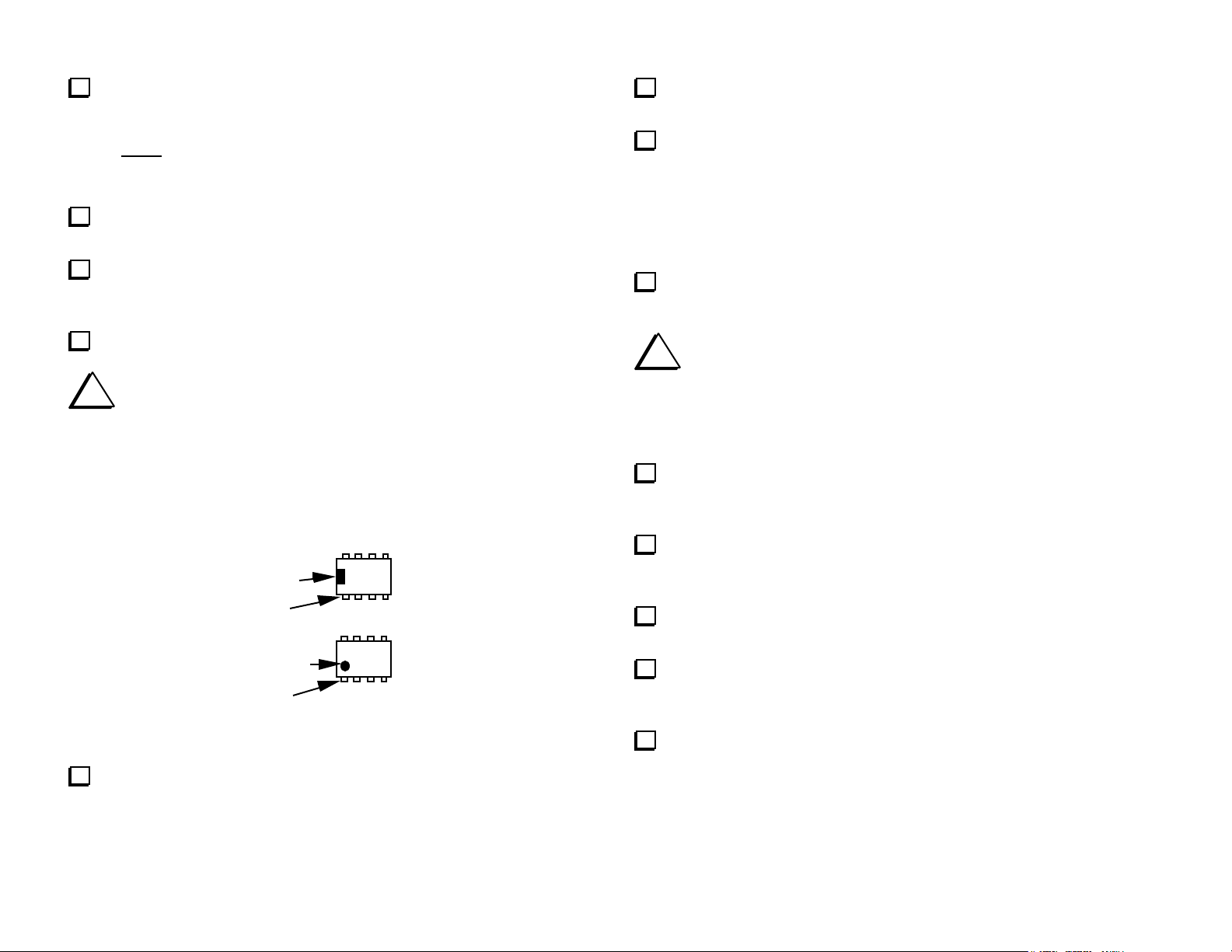
Note: The pin 1 end of ICs can be identified by a notch or dimple as
shown in Figure 6. This end must be oriented toward the notched end
of the component outline.
Notch
Pin 1
Dimple
Pin 1
Figure 6
Install U5 (LM358, 8 pins), which is located on the top side of
the board, left of the "KPA100" label. A portion of the part number is
printed on the board under the IC ("358"). Do not solder yet.
__ U2, TD62083 __ U6, EL5146
__ U4, MAX1406 __ U7, LMC6482
Install the 28-pin IC socket at U1. The notched end of the socket
must be aligned with the notched end of its outline.
i
In the following steps you'll be installing several
connectors at the back edge of the PC board (top side). These
connectors must be installed correctly in order for the rear
panel to fit onto the PC board. Figure 32 (page 38) shows how the
rear-panel connectors will appear once installed.
Install the external speaker jack, J6, at the back edge of the
board. Solder the center pin only. Make sure that the jack is pressed
down flat against the board while soldering.
If J6 does not appear to be aligned with its PC board outline, or it
is tilted, re-heat the center pin while adjusting the connector's
position. Once it is positioned correctly, solder the other two pins.
Locate screw terminal E1. If it was supplied with a screw, remove
it. The screw will not be used.
Place E1 in its indicated position, with the threaded hole facing
the rear edge of the board. Solder just one pin. CAUTION: This
part will get hot; don’t touch it with your finger while soldering.
If necessary, reheat the soldered pin of E1 and adjust it so that all
four pins are pressed down on the board as far as they'll go. Then
solder all pins.
18
Page 19
Install the RCA jack, J7. The small plastic standoffs on the
bottom of the connector should be inserted in the holes provided.
While soldering, hold J7 flat against the board, and keep it centered
within its component outline. Clip the leads on the bottom side.
Locate J8, the 9-pin "D" connector, and temporarily place it in
its indicated location (far right side of the board). Note that the leads
of capacitors C97-C99 on the bottom of the board interfere with the
proper seating of J8. To avoid this, you will need to trim off the
plastic extensions on both sides of the connector. First, bend upward
and cut off the thin metal tabs above the plastic extensions (do not use
flush cutters for this--you may damage them) . Then trim the plastic
away so that it doesn't interfere with the leads of C97-C99.
Install J8 and solder just one of the 9 pins. Adjust the position of
J8 as you did for the other connectors, making sure the connector is
flat against the board. Then solder the remaining pins.
i
You may have received two 16F872 microcontrollers with
your kit. The one marked "KPA100" or "PA" should be used here.
Before handling U1 (16F872), touch a grounded surface.
Straighten the leads of U1 (PIC16F872) as shown below. The rows
of pins must be straight and parallel to each other to establish the
proper pin spacing. To straighten the pins, rest one row of pins against
a hard, flat surface. Press down gently on the other row of pins and
rock the IC forward to bend the pins into position as shown below.
Insert U1 into its socket, with the notched or dimpled end of the
IC aligned with the notched end of its component outline.
Examine U1 closely. If any pins are bent, remove the IC and
straighten them. (To remove U1 from its socket, pry it up gently on
each end using a small flat-blade screwdriver.)
Visual Inspection
i
Nearly all problems with kits are caused by poorly-
soldered component leads or incorrectly-installed components.
You can locate and correct most assembly errors ahead of time
with a simple visual inspection. This is especially important at
high power levels, where an unsoldered or reversed component
could cause damage to the power transistors.
closely for all of the following: cold solder joints (dull rather than
shiny appearance), solder bridges, and leads that are not soldered. Reheat any suspect joints.
re-check the orientation of all __ Diodes, __ Transistors, __ ICs.
Using a magnifying glass, examine the bottom of the PC board
Using the parts placement drawing at the end of the appendix,
Flared
Straight
Figure 7
19
Page 20
Initial Tests
Make the resistance measurements listed below, touching the
DMM's (+) and (-) leads to the indicated points. The (-) lead will go to
ground in all cases except the first measurement (relay coils).
i
The symbol > means greater than. Your DMM may indicate
infinite resistance (all digits flashing) for readings that are listed as
"> 10 k." (Do not use an analog VOM.) Other readings should be
+/- 10 %. K4 reads higher resistance than the other relays because K3
is not yet installed (the two coils are in parallel).
KPA100 Test Points (+, -) Resistance
(+) and (-) leads of relays K1,K2,K4-K12
(on bottom of board, marked)
U1 pin 1, ground > 1 k
U1 pin 2, ground > 10 k
U1 pin 3, ground > 10 k
U1 pin 4, ground 3.1 k
U1 pin 13, ground > 10 k
U1 pin 14, ground > 10 k
U1 pin 27, ground > 10 k
U1 pin 28, ground > 10 k
U4 pin 1, ground > 10 k
U4 pin 8, ground > 10 k
"AF" pad (measure from bottom), ground > 10 k
D10 banded end, ground > 10 k
Determine what revision of firmware your K2 has installed at
present by turning the K2 on while holding any switch. Record the
number shown at the left end of the LCD (e.g., 2 . 0 1 H ): _______.
Turn off the K2. Disconnect all external cables.
Remove the six K2 top cover screws shown in Figure 8.
Remove the top cover. Disconnect the speaker and all options.
Store the top cover in a safe place to protect the finish.
650-800 (K4)
325-400 (others)
i
You can easily remove the KPA100 and re-install the original
top cover at any time, returning the K2 to its low-power field
configuration.
1 2
3 4
5 6
Figure 8
i
Before handling the Control board in the following
steps, touch a grounded surface.
panel board. Also remove the KAF2 audio filter board if present.
the Control board up at the point marked "LIFT HERE" on the RF
board. Then unplug the Control board. Place it in front of you with the
component side up.
the voltage selector switch, S1. If the present value of this capacitor is
.01 µF ("103"), replace it with an 0.1 µF capacitor ("104"). Use a
capacitor with 0.2" lead spacing. Note: If you have an older Control
board (rev XC) that does not include C42, solder the 0.1 µF capacitor
between pins 4 and 8 of U3 (LMC6482, on the Control board).
Remove the screws that hold the K2 Control board to the front
Use the long-handled Allen wrench supplied with the K2 to pry
Locate C42 on the K2 Control board (CTRL-C42), which is near
20
Page 21

i
A ribbon cable is used to connect the KPA100 board to the K2
Control board. To ensure correct cable orientation, keying inserts are
used. This requires cutting one pin on the male connectors at each end.
The pin to be cut, 8T (8-volt transmit), is not used by any Elecraft
option. If you need 8T for any reason, skip the next three steps, as
well as the last step on this page.
The main microcontroller (U6, K2 Control board) must
have revision 2.02A or later firmware in order to control the
KPA100. If your firmware revision (recorded on the previous page) is
older than this, you'll need to install a new microcontroller. This 40pin IC should have been supplied with your KPA100 kit. Refer to the
K2 Revision 2 Firmware manual for installation instructions.
Locate P4 on the Control board, a 10-pin, dual row (5 x 2) male
connector (see Figure 9). P4's pins are numbered left to right, top to
bottom (pin 2 is to the right of pin 1, pin 3 is below pin 1, etc.).
P4
1
P5
S1
Cut Pin 4
Figure 9
Cut pin 4 of P4 as indicated above, as close as possible to the
connector's plastic body. The best way to do this is to grasp the pin
with long-nose pliers, then bend it repeatedly until it breaks off.
Cut pin 4 of P1 on the KPA100 board (see Figure 10).
Cut Pin 4
If you plan to use computer control of your K2 via the KPA100's
RS232 interface, and have not previously installed the KIO2 option,
you may need to modify the Control board (see page 51). Making the
modification now will save you the trouble of removing the Control
board again later.
Plug the K2 Control board into the RF board. Make sure that all
three connectors along the bottom edge of the board are plugged into
their mating connectors.
Re-install the KAF2 board if applicable. Secure the Control board
to the Front Panel board with the hardware removed earlier.
Locate the pre-assembled ribbon cable. Lay the cable flat as
shown in Figure 11, with the black wire at the top and the
connector holes facing up.
Black Wire
R31
C25
P1
Figure 10
Pin 1 Mark
GNDAF
Pin 1 Mark
Figure 11
1
Install keying inserts in position 4 of both connectors. The
inserts include break-off tabs that aid installation. The inserts should
lock in place and be flush with the mating surface of the connector.
21
Page 22

i
The cables that connect the KPA100 to the K2 are all kept
short to avoid pickup of stray RF. Because of this, the KPA100
assembly must be placed on top of a 3 to 4 inch (7 to 10 cm) platform
to the right of the K2 during test and alignment. You can use books, a
cardboard box, etc. Do not use metallic objects.
Place the KPA100 on a suitable platform as described above. The
front edge of the KPA100 board should be facing toward you (speaker
cutout to the right).
Plug one end of the ribbon cable into the Control board at P4.
The correct end can be determined from Figure 12. The black wire
should be oriented toward the lower end of P4 (away from pin 1). If
the indicated end of the ribbon cable cannot be plugged in at P4, the
keying insert may be installed at the wrong position.
GND
12 K2
P1
Pin 1 Mark
P5
P4
Black Wire
S1
Figure 12
Plug the other end of the ribbon cable into the KPA100 at P1.
The correct orientation is shown in Figure 13.
The SSB option microcontroller (U1, KSB2) must have
revision 1.06 firmware or later. Check the label to determine the
revision. If it's older than 1.06, a new 28-pin IC (16C72A or 16F872)
should have been supplied with your KPA100 kit. Install it at this
time, with pin 1 of the IC oriented toward the left side of the K2.
Ribbon Cable
To Control
Board, P4
SPKR
GND
GND
AF
Figure 13
Connect a 12-14 volt power supply or battery to the K2's DC
input jack (DC barrel connector, J3 on the RF board).
Turn on the K2; you should see E L E C R A F T on the LCD,
followed by N O P A P S . This message is a reminder that no high-
current power supply is connected to the KPA100 yet. You may also
hear relays switching on the KPA100 (in addition to the K2 relays).
Tap D I S P L A Y to check the K2 power supply voltage (E) and
current (i). If the voltage is lower than expected, or the current is over
0 . 5 0 amps, refer to Troubleshooting (page 56 of this appendix).
Note: Installing the KPA100 increases K2 receive-mode current drain
by approximately 100-200 mA. In transmit mode, additional current is
drawn, but this will not be included in the voltage/current display.
Tap D I S P L A Y until the frequency display returns.
22
Page 23

Set your DMM for DC volts, 20 or 30 V full scale (or auto
Downloaded by
RadioAmateur.EU
ranging). Connect the DMM's (-) probe to the ground jumper on the
KPA100 board (near U1). Using the DMM's (+) probe, make the
voltage measurements listed below. Voltages should be within +/- 10%
except as noted.
i
When making measurements at IC pins, be careful not
to short adjacent pins. Use only a fine-tip DMM probe. Do not
attempt to make measurements using a wire or a probe with a
large, blunt tip.
KPA100 Test Point (+) Voltage
U1 pin 1 5.0
U1 pin 7 0 to 0.1
U1 pin 13 0 to 0.1
U1 pin 14 0 to 0.1
U1 pin 15 0 to 0.1
U1 pin 20 5.0
U1 pin 27 5.8
U1 pin 28 5.7
U2 pin 10 12-15
U4 pin 1 12-15
U4 pin 11 5.0
U5 pin 1 0 to 0.1
U5 pin 7 0 to 0.1
U6 pin 1 0 to 0.1
Tap M E N U , then tap D I S P L A Y to bring up the K2's secondary
menu (S E C will be flashed). This menu is used to configure various
features that are available in K2 revision 2 firmware.
Use the VFO knob or the B A N D + / B A N D - switches to scroll to
the P A menu entry. If you see P A - - , the KPA100
microcontroller is not communicating properly with the K2. Refer to
Troubleshooting.
The P A parameter will probably be set to O F F initially. Hold
E D I T to highlight the parameter, then scroll until you find an entry
starting with E (error status). The error status should be E 1 2 , where 1
indicates that the KPA100 is in bypass (QRP) mode, and 2 indicates
that no KPA100 power supply is present. If you see any other error
numbers, see Error Status in the Troubleshooting section.
Set the P A parameter to O N . Tap M E N U to return to menu
scroll mode.
Tap D I S P L A Y to return to the primary menu (P R I will be
flashed). Tap M E N U again to return to the normal frequency display.
Turn off the K2 and disconnect the power supply.
Disconnect the KPA100 end of the ribbon cable.
23
Page 24

Assembly, Part II
A number of toroidal inductors are used on the KPA100 PC board.
The first inductor to be wound uses a type T44-2 core. The letter T
identifies an iron-powder core. 44 specifies the outside diameter in
hundredths of an inch, in this case 0.44 inches (11.2 mm). The -2
suffix refers to the core type and color, in this case a red iron-powder
core.
There are also two ferrite toroid cores used, such as type FT37-61. In
this part number, FT identifies the core as ferrite, and 37 is the size
(0.37", 9.5 mm). The -61 identifies the type of ferrite, although all
the ferrite cores are dark gray in color. (There are also two "binocular"
ferrite cores in the kit, which will be described later.)
Three types of enamel wire are supplied with the kit: #22 red, #26 red,
and #26 green. #22 wire is much larger in diameter than #26. Be sure
to use only the type called for in the instructions; do not substitute
other wire types. Cut wires to the specified lengths to avoid running
out of wire.
1
Cut 13 inches (33 cm) of #22 red enamel wire. To wind L18,
"sew" the long end of the wire through the T44-2 core. Each pass
through the core counts as one turn. 14 turns are needed, as shown in
Figure 14. The enamel insulation will be removed in a later step.
Remove insulation
Figure 14
Seven red iron-powder toroid cores are supplied with the kit. Four
of these are type T50-2 (0.5" [12.7 mm] dia.), and three are smaller,
type T44-2 (0.44" [11.2 mm] dia.). Locate a T44-2 core for use at
L18.
Find the component outline for L18, at the right side of the board
near the cutout for power transistor Q1. Compare this component
outline to Figure 14, which shows two views of a typical toroidal
inductor. L18 will be mounted vertically as shown at the right side of
the drawing, with one wire exiting at the core’s upper left, and the
other at the lower right.
i
#22 enamel wire is fairly stiff, and may be difficult to
wind tightly onto the core. The turns should not be loose, but it
is acceptable to have a very small gap between the wire and the
core's flat surfaces. If you try to wind #22 so that it "hugs" the
core all the away around, you may have to pull the wire too
hard, resulting in hand fatigue.
1
Pre-wound toroids are available from an Elecraft-approved source; see page 3.
Verify that the turns of L18 are not bunched together. They
should be evenly spaced, and should occupy about 80-90% of the core.
Typical turns spacing is shown in the photograph below (Figure 15).
Figure 15
Toroids shown in photos are wound on white cores to highlight
turns counts and spacing. Place L18 on top of the photo above,
then adjust the turns spacing until it is similar to that shown.
24
Page 25

i
of solder (a "blob") on the end of your soldering iron, then insert the
clipped end of the wire into the hot solder. If the iron is hot enough,
you should see the insulation bubble after 4 to 6 seconds. Add more
solder and feed more of the wire into it as the enamel melts. Continue
tinning the wire up to slightly past the edge of the core. Then slowly
pull the wire out of the solder. If any enamel remains on the lead,
scrape it away using your thumb and forefinger. You can also burn the
insulation off by heating it with a butane lighter for a few seconds,
then use sandpaper to remove the enamel residue. If you scrape the
insulation off with a razor blade, avoid nicking the wire.
from the leads up to the edge of the core (see Figure 14).
adhering very well, remove any residual enamel and re-tin the lead.
leads taut on the bottom of the board.
solder binds well to the leads. If the lead appears to be an "island"
in a pool of solder, it is not making good contact; remove the
toroid and prepare the leads as described above. (For further
information, look for "Soldering Tips" on our web site.)
between L18's pads (not the leads) on the bottom of the board. If the
reading is over 1 ohm, re-strip the leads. Note: Your DMM probes will
have some residual resistance. Short them together to measure this
amount, and subtract it from your continuity readings.
The enamel wire can be heat-stripped. Place a small amount
Strip the leads of L18 as described above. Remove the enamel
Tin L18's leads. If the solder on the leads looks dull or is not
Install L18 vertically as shown by its component outline. Pull the
Solder the leads of L18. When soldering, make sure that the
i
Do not apply adhesives or fixatives of any kind to toroids.
Using your DMM on a low resistance scale, check for continuity
__ L1: 27 T, RED __ L2: 25 T, RED __ L4: 17 T, BLK
22" (56 cm) 21" (53 cm) 15" (37 cm)
__ L5, 16 T, BLK __ L6, 16 T, BLK __ L7, 11 T, BLK
14" (36 cm) 14" (36 cm) 10" (26 cm)
__ L8, 10 T, BLK __ L10, 9 T, BLK __ L11, 8 T, BLK
9.5" (24 cm) 9" (23 cm) 8" (20 cm)
The low-pass filter toroids are shown in the photos at right
(Figure 16). Wind each of these toroids using the indicated powderediron cores, either RED (T50-2) or BLACK (T50-10). All are wound
using #22 enamel wire. Use the wire length and number of turns shown.
Prepare the leads of these toroids as you did for L18.
__ L12, 8 T, BLK __ L13, 21 T, RED
8" (20 cm) 18" (45 cm) 17" (43 cm)
Figure 16
__
L14, 20 T, RED
25
Page 26

Place each of the low-pass filter toroids on its photo and adjust
the turns spacing so it is similar to that shown. Re-check turns counts
and core colors. (Each pass through the core counts as one turn.)
i
Good electrical contact between toroid leads and their
pads is critical for safe and reliable operation at high power
levels. If you see any indication that the solder is not binding
well to a lead, remove the toroid and prepare the leads again.
Install L1 vertically as indicated by its component outline (near
relay K3).
Prepare the leads of L15 and L16 as before.
Install L15 and L16, located near relay K2.
Locate the two dark gray (ferrite) toroid cores. The smaller of
the two (type FT37-61) has a diameter of 0.37" (9.5 mm). This core
will be used in the following steps.
i
Toroidal transformer T3 uses a bi-filar winding, which means
that two wires are wound on the core together. The wires will be
twisted together loosely before they're wound onto the core.
Install and solder the remaining low-pass filter toroids. Match
each of the low-pass filter toroids to its reference designator carefully.
Exchanging any of them will result in poor performance on two or
more bands.
On the bottom side of the board, check for continuity between
the pads of all the low-pass filter toroids. If you get a reading of > 1
ohm, remove the toroid from the board and prepare the leads again.
Two more T44-2 cores (red, 0.44" [11.2 mm]) will be used at
L15 and L16. Cut two 24" (61 cm) lengths of #26 red enamel wire
(the smaller gauge red enamel wire). Wind 29 turns on each inductor as
shown in Figure 17.
Cut two 8" (20 cm) lengths of #26 enamel wire, one red and
one green.
Twist the red and green wires together over their entire length.
The wires should cross over each other about every 1/2" (1 cm).
Wind 7 turns of the twisted wires onto the small ferrite core
(FT37-61). The turns should be spaced to cover about 80-90% of the
core, as shown in Figure 18. Note: To make the turns spacing easy to
see, the wires shown in the photo were not twisted together.
Separate T3’s leads as shown in Figure 19. The numbers on the
leads correspond to numbered pads on T3's PC board outline.
Figure 18
Figure 17
Strip and tin the leads of T3. (Figure 18 shows T3 with its leads
tinned.) Keep the red and green leads spaced slightly apart during
stripping and tinning.
26
Page 27

Using a magnifying glass, examine the red/green lead pairs to
(GRN)
(GRN)
(GRN)
(GRN)
make sure that the leads are not shorting together near the core.
Install T3 vertically on the PC board as indicated by its outline
(near the microcontroller, U1). Insert the red and green leads into
their numbered holes as shown in Figure 19. Pull the leads taut on the
bottom, then solder.
Separate T4’s leads as shown in Figure 21. The numbers on the
leads correspond to numbered pads on T4's PC board outline.
Figure 20
4
1
(RED)
3
2
(RED)
Figure 19
Verify continuity between the #1 and #4 pads of T3. If you get a
reading over 1 ohm, remove T3 and prepare the leads again.
Transformer T4 also uses a bifilar winding. Cut two 11" (28 cm)
lengths of #26 enamel wire, one red and one green. Twist the red and
green wires together as you did for T3.
Wind 12 turns of the twisted wires onto the large ferrite core
(FT50-43). The turns should cover about 80-90% of the core, as
shown in Figure 20.
Strip and tin the leads of T4.
Using a magnifying glass, examine the red/green lead pairs to
make sure that the leads are not shorting together.
4
1
(RED)
2
3
(RED)
Figure 21
27
Page 28

Install T4 vertically on the PC board as indicated by its outline
near the small notch (back edge). Insert the red and green leads into
their numbered holes as shown in Figure 21.
i
T4's leads are numbered differently from T3's. Be sure
to insert the leads into the correct numbered holes in the PC
board, or the SWR bridge will not properly indicate forward
and reflected power. This could result in damage to the power
transistors.
Verify continuity between the #1 and #4 pads of T4.
i
Figure 22 (page 29) shows the connectors and other hardware
that will be attached to the rear panel in the following steps. The
antenna jack (J2), DC power jack (J3), and fan will be secured to the
panel first, then the rear panel assembly will be attached to the
KPA100 PC board.
Unwrap the rear panel. Orient it with the antenna jack at the left.
i
Always use bright (zinc-plated) hardware unless an
item is described as black in the instruction step.
i
In the next step, do not use a small-gauge component
lead for Z1. Use a lead from a 1N4007 diode or 3-watt resistor.
Locate the two ferrite beads (gray). Slip the two beads onto a bare
component lead (see above). Install this assembly at Z1, which is near
the hole for RF power transistor Q1. Form the leads to match the
indicated pad spacing.
Attach the antenna jack, J2 (SO239) to the rear panel as shown
in Figure 22. Use four 4-40 x 1/4" (6.4 mm) pan head screws, one
solder lug, three #4 split lock washers, and four 4-40 nuts. As shown
in Detail A1, the solder lug takes the place of one lock washer. The lug
must be installed on the screw nearest the top edge of the rear panel.
Do not overtighten the hardware.
Locate the four fan mounting holes (countersunk from the inside
of the panel). Test a 4-40 flat-head screw at each screw location, and
remove any burrs that might be obstructing flush seating of the screw
head.
A small hole is provided near one of the countersunk holes for
routing the fan wires. Insert the fan wires into this hole, and orient the
fan as shown. The label side of the fan should face away from the
panel.
28
Page 29

E1
Downloaded by
RadioAmateur.EU
J7 J6
Fan Wires
BLK
RED
FAN
B1
J8J3J2
A1
A2
RED
B3
J2
J3
BLACK
5
T4
6
GND
B2
Figure 22
29
Page 30

Cut the two fan wires to a length of 2" (5 cm), measured from
where they exit the fan's frame. Remove 1/4" (6.4 mm) of insulation
from each wire, then twist together and lightly tin the strands.
Cut two lengths of #20 insulated hookup wire: one black, 1.5" (4
cm) long; and one red, 1.25" (3.2 cm). Remove 1/4" (6 mm) of
insulation from each end of both wires.
Secure the fan to the rear panel using four 4-40 x 9/16" (14.3
mm) flat head screws, four #4 split lock washers, and four 4-40 nuts.
Note: The screws may not extend through to the ends of the nuts, but
the nuts should still be secure with 2-3 threads. Avoid tightening the
screws further, as this could distort the fan's plastic frame.
Locate two DC input connector housings, one red and one black.
Hold the two connectors in the orientation shown in Detail B1 of
Figure 22. Look closely at the sides of the connectors. Each has a
small tongue on the right side, and a groove on the left.
Slide the tongue on the right side of the red housing into the
groove on the left side of the black housing. Make sure the housings
are mated exactly as shown in Detail B1, with the black housing to the
right and the "hoods" at the front of the connectors facing up. Make
sure the interlocking tongue and groove are fully meshed.
Install right-angle PCB pins into the housings (Detail B2). The
long end of the pin should be inserted into the housing until it snaps
into position, and the short end must point down. When the pin is
correctly inserted, the distance from the back end of the housing to
the bend in the pin will be exactly 0.4" (10 mm).
Insert the paired housings through the rectangular rear-panel hole,
with the red housing aligned with the "+" label.
Solder one end of the red wire to the center pin of the antenna
connector (J2) as shown in Figure 22, Detail A2. Remove any excess
solder from the outside of the pin using desoldering braid.
Solder one end of the black wire to the solder lug.
Make a 1" long jumper using a discarded component lead (from a
small resistor or capacitor). Solder one end of this jumper to the center
pin of J2, as close to the body of the connector as possible (Detail
A2). Leave the other end free, oriented as shown.
Remove the finishing nut from the external speaker jack (J6).
Install the rear panel assembly onto the KPA100 PC board,
threading J2's red wire through the center of transformer T4.
At the same time, insert J3's leads into their holes.
Secure J6 (EXT SPKR) to the rear panel with its finishing nut.
Secure J8 (AUX I/O jack) to the rear panel using two male-female
standoffs. Do not overtighten the standoffs.
Secure E1 (GND) to rear panel with the 6-32 thumbscrew, 6-32
nut, and two #6 flat washers. The nut must be installed between the
washers and thumb screw as shown to ensure good electrical contact.
Use two E-shaped brackets to hold the housings in place, as shown
in Detail B3 (one from above, one from below). Secure the brackets to
the rear panel using two 4-40 x 1/4" (6.4 mm) flat head screws, two #4
split lock washers, and two 4-40 nuts. This hardware is shown in Figure
22 (at top).
i
The rear panel should now be flush with the back edge of the
PC board. If not, one of the connectors may not be properly installed.
Solder J3's leads to the board. These connections are critical to
reliable operation. The solder should coat J3's pads on both
sides of the board, and the joints should be clean and shiny.
Trim J3's leads on the bottom of the board.
30
Page 31

Solder the red fan wire to the pad labeled "FAN+" (near J6).
Solder the black fan wire to the "FAN-" pad.
Top
Route the fan wires away from RFC1.
Solder J2's wires to the points indicated in Detail A2 of Figure 22.
The red wire goes to T4 pin 5, black wire to the pad labeled "GND"
near E1, and bare wire jumper to T4 pin 6.
Locate a large 100-µH RF choke ("101") for use at RFC10 (0.75"
lead spacing). Position the RF choke as close as possible to the rear
panel as shown in Figure 23. Solder RFC10 to the center pin of J2 and
the grounded solder lug using short leads.
RFC10
101
Figure 23
Examine the area around J2 closely to make sure that none of the
wires running to the center pin are contacting nearby hardware.
Locate the smaller binocular coil form for use at T1. As shown in
the side view, Figure 24a, the ferrite core is offset upward slightly,
leaving a gap at the bottom. The end view, Figure 24b, identifies
contacts 1 and 3. The other end is contact 2.
1
(a)
(c)
2
(b)
3
1 3
Figure 24
Place T1 at its indicated location, with the gap (bottom side)
toward the PC board. Contacts 1, 2, and 3 must be aligned with their
PCB pads. Figure 24c shows all of T1's pads (1-5).
i
T1 is very difficult to remove once installed. While
soldering, make sure it is centered directly over its component
outline and is seated flat against the board. T1 may be just
slightly larger or smaller than the indicated outline.
Using a heavy solder iron (pencil or gun), solder only contact 1 of
T1 to the board. Solder over the full length of the contact.
If T1 is not centered, reheat contact 1 and adjust its position.
Solder contacts 2 and 3. Solder along the full length of each
contact.
4
5
31
Page 32

There are two sizes of Teflon wire (gray): #18 (larger) and #22
(smaller). The smaller size will be used at T1, and the larger at
T2. Cut a 9" (23 cm) length of the #22 Teflon wire.
Remove 1/4" (6 mm) of insulation from one end, then twist the
strands together. Tin the strands using a small amount of solder.
Solder the Teflon wire to the pad labeled T1-4.
Thread the wire through the core (1 turn) as shown in Figure 25a.
You'll then have one loop of wire on the left side of the core.
Add a second turn by passing the free end of the wire back
through both holes in the core, as you did in (a). Pull on the wire so
that the winding is tight. The winding should then look like Figure 25b,
with two loops on the left side.
Add a third turn, again passing the free end back through both
holes in the core (Figure 25c). Pull the wire to tighten the winding.
Count the loops on the left side to make sure you now
have exactly three. There will be two loops on the right side, plus
the two ends of the wire.
Cut the free end of the wire to a length of 5/8" (16 mm),
measured from where it exits the core. Remove 1/4" (6 mm) of
insulation, then tin and twist the leads.
4
1
(a)
4
2
(b)
Solder the wire to the pad labeled T1-5.
32
3
(c)
Figure 25
4
5
Page 33

Locate the larger binocular coil form for use at T2. Note: T2 may
vary in length from 1" to 1 1/8" (25 to 29 mm). The given pads can
accommodate either length. Figure 26 shows all five of T2's pads.
Cut an 18" (46 cm) length of #18 Teflon wire (gray). Remove
1/4" (6 mm) of insulation from one end, then twist and tin the strands.
Solder the Teflon wire to the pad labeled T2-5.
Thread the wire through the core (1 turn) as shown in Figure 27a.
5
2
4
Figure 26
Center T2 at its indicated location with the gap (bottom side)
toward the board. Contacts 1-3 must be aligned with their PCB pads.
i
Once T2 is installed, it is nearly impossible to remove.
While soldering T2, make sure it is centered directly over its
component outline and is seated flat against the board.
Using a heavy solder iron, solder contact 1 to its pad over just a
small portion of its length.
1
3
Add a second turn, pulling the wire so that the winding is tight.
The winding should look like Figure 27b (2 loops on the right).
Add two more turns (c), (d). Pull the wire to tighten the winding.
There should now be exactly four loops on the right side.
Cut the free end of the wire to a length of 1 1/4" (32 mm),
measured from where it exits the core. Remove 1/4" (6 mm) of
insulation, then tin and twist the strands. Solder the wire to T2-4.
5
5
1
(a) (b)
5 5
2
If T2 is not centered over its component outline, or is tilted,
reheat contact 1 and adjust T2's position.
Solder contact 3 over its full length.
Solder contact 2 over its full length. Keep the iron tip away from
nearby components, especially potentiometers R26 and R27.
Solder contact 1 over its full length.
33
3
(c) (d)
Figure 27
4
4
Page 34

Install the following resistors near T1. Note: Three sizes of 10ohm resistors are to be installed, one rated at 1/4 watt, one rated at 1
watt, and three rated at 2 watts. Compare the sizes ahead of time.
__ R9, 10 ohms, 5%, 1/4 W (brown-black-black)
__ R34 and __ R35, 10 ohms, 2 W
__ R19 and __ R20, 3.6 ohms, 2 W
__ R23, 10 ohms, 1 W (brown-black-black)
__ R22, 100 ohms, 3 W
__ R21, 10 ohms, 2 W (form leads to fit given pad spacing)
Install relay K3, located near T2.
Install the following capacitors in the low-pass filter area:
__ C2E, 1000 pF, 500 V silver mica
__ C2A, and __ C6D, 1200 pF, 500 V silver mica
__ C2C, 2200 pF, 500 V silver mica
Install the following capacitors, located in the area between the
two power transistors.
__ C58 and __ C59, 0.1 µF (104), 0.2" lead spacing
__ C80 and __ C81, 4700 pF (472), 0.25" lead spacing
34
Page 35

Unwrap the heat sink and place it on a soft, clean surface to
protect the finish. Orient it with the speaker hole at top left and fins
facing down (Figure 28). The raised area on the right side is the
pedestal, where the power transistors will be mounted. The PC board
will be mounted at the seven points marked H and S.
i
The heat sink has a non-conductive, black anodized
finish. To ensure good electrical contact between the heat sink
and PC board, the finish will be removed at the seven points
shown at right. When working with the heat sink, be careful
not to nick or scratch the fins (on the opposite side).
Attach a portion of the supplied sandpaper (no more than 1/4th of
the sheet) to a flat piece of wood or a sanding block. The block should
be at least 4" long and 1" wide (10 x 2.5 cm).
Locate the two machined standoffs on the pedestal, labeled S in
Figure 28. Lay the sanding block across the top surfaces of both
standoffs. Keeping the block parallel to the pedestal at all times,
carefully sand off just enough of the black finish to expose the top
surfaces of the standoffs. Do not remove any further material,
since this may affect proper spacing of the power transistors.
Use the sandpaper (but not the sanding block) to remove the
finish around the holes labeled H in Figure 28. The area of finish
removed should be approximately centered over each hole, and at least
1/4" (6 mm) in diameter. Note: You can also scrape away the
anodization with a sharp tool or a hand mill (Dremel tool) with a wirebrush attachment. Be careful not to cut down into the aluminum.
Locate the 7 set screws (4-40 x 1/2") and the small hex wrench.
Thread a set screw into each hole marked H or S, being very careful
not to cross or strip the threads during insertion. Tighten the set
screws using the hex wrench.
S
H
H
Pedestal
H
H
H
Figure 28
i
The leads of some components near the power
transistors must be flush-trimmed as explained in the next
step. This will prevent leads from shorting to the pedestal.
Flush-trim the leads of the components listed below on the
bottom of the board. The leads must be less than 1/32" (0.7 mm) long.
__ C40 __ C50 __ C80 __ C81
__ C58 __ C59 __ L18 __ C31
__ Z1 __ L16
S
Thread 3/16" dia., 3/16" long standoffs onto the five set screws
marked H. Do not use lock washers. Tighten the standoffs using
pliers, but do not over-tighten.
Using your DMM's lowest resistance scale, check for continuity
(< 1 ohm) between one set screw and all of the others.
Over the rest of the board, trim any component leads that you
may have missed earlier, including connector leads. Use a ruler to make
sure that all leads are trimmed to less than 1/8" (3 mm).
35
Page 36

i
The PC board will be attached to the heat sink
temporarily in the next step. This will position the power
transistors correctly for soldering. Do not install thermal pads
at this time.
Place the KPA100 PC board assembly on top of the heat sink.
Secure the board to the heat sink at the pedestal set screws using 1/2"
(12.5 mm) long standoffs. Thread them on hand-tight only.
Locate the two flange-mount power transistors. If the tabs are
bent, straighten them carefully using long-nose pliers.
Pre-tin the tabs of Q1/Q2 (top and bottom) with a small amount
of solder. Also pre-tin the pads for Q1 and Q2 on the PC board. A
high-wattage iron will be required to tin the emitter pads.
Place power transistors at Q1 and Q2, orienting the four tabs as
shown in Figure 29a. The notched tab must be aligned with the
PCB pad labeled "C" (collector).
i
Use an iron with a large tip when soldering the
emitters of Q1 and Q2. A small tip cannot supply enough heat.
Solder all four tabs of Q1 and Q2 to their pads. The solder should
coat the entire tab and the PC board pad surrounding it (Figure 29b).
Remove the screws from Q1 and Q2.
Remove the standoffs holding the PC board to the heat sink, then
remove the board.
Wrap the heat sink back up and set it aside.
Install 68-ohm, 2-watt resistors at R38 and R39. These resistors
straddle the adjacent emitter leads of Q1 and Q2. Form the leads to
match the pad spacing, and keep the resistors spaced slightly apart.
Solder R38 and R39, then flush-trim the leads.
Locate a 1200-pF silver mica capacitor (C83). Trim the leads to
exactly 1/8" (3 mm) long.
(a)
(b)
E
C B
E
Figure 29
Secure Q1 and Q2 to the pedestal temporarily using four 4-40 x
1/4" (6 mm) pan head screws and four split lock washers. The lock
washers must be used, or the screws may bottom out.
Place C83 in exactly the position shown in Figure 30, near the
"R38" and "R39" labels. Solder C83 to the tops of the indicated
pads. Do not insert the leads into the holes.
R39
R38
(a)
Figure 30
36
(b)
Page 37

i
Figure 32 (page 38) shows wiring details for J1, J4, and J5.
Refer to this illustration while completing the following steps.
As shown in Figure 32, two types of 2-pin connector housings are
supplied: 0.156" pin spacing for use at J1 and J4, and 0.1" spacing for
J5. Also supplied are small and large crimp terminals (see parts list
photos). Locate the smaller of the housings and two of the small crimp
terminals for use at J5.
Cut a 4.5" (11.5 cm) length of RG-174 coaxial cable. Using a
sharp tool, remove about 3/4" (2 cm) of the coax jacket from each
end (see Figure 31). Be careful not to nick the braid.
Figure 31
Cut a 6" (15 cm) length of two-conductor speaker cable (small
gauge, with clear insulation). Split the conductors at both ends, then
remove 1/4" (6 mm) of insulation from all four wires. Avoid nicking
or tearing the wire strands when removing the insulation.
Twist each wire's strands together, then tin the wires, using a very
small amount of solder (just enough to hold the strands together).
Attach crimp terminals to the two wires at one end as shown in
Figure 32 (Detail A). Before soldering, fold the small flaps of the
terminal closed using long-nose pliers. This will hold the wire in place.
i
When you insert crimp terminals into the housing in the next
step, they should snap into place. Each terminal has a small retaining
tab on the back that latches into a hole in the housing. The location of
the retainer and its hole in the housing are shown in Detail B.
Figure 32 shows J5 with the wires attached, and the small guides
on the connector facing down and away from you. Hold the connector
in this orientation, then insert the silver wire into the right hole of
the housing until it snaps into place. Insert the copper wire into the
left hole. Verify that the retainer tab is locked in place (Detail B).
Insert the wires at the other end of this cable into the pads labeled
AF (silver wire) and GND (copper wire) on the KPA100 board. Insert
the wires all the way up to the insulation to avoid leaving any exposed
lead length. Solder both wires.
Locate the two larger 2-pin housings and four of the large crimp
pins for use at J1 and J4.
Separate the braid (shield) from the center conductor at both
ends. Clip off about half the strands of the braid close to the jacket,
then twist the remaining braid into a thin bundle.
Remove a small amount of insulation from the center conductor.
Use long-nose pliers to hold the center conductor while stripping it.
Solder the center conductor and shield to crimp terminals.
Insert the terminals into a 2-pin housing as shown in Figure 32
(center conductor on the left, braid on the right).
Solder the other end of the coax cable to the two pads labeled "RF
IN" and "GND" on the KPA100 board (near relay K1). The shield
goes to "GND".
Cut two 4.5" (11.5 cm) lengths of #20 AWG stranded insulated
hookup wire, one red and one black. Remove 1/4" of insulation from
each end of both wires.
Twist the strands together tightly, then tin the wires. Use a very
small amount of solder.
Solder one end of each wire to a large crimp terminal.
Insert the terminals into a large 2-pin housing as shown in Figure
32 (black wire on the left, red wire on the right).
Solder the free end of the red wire to the pad labeled "12K2" on
the KPA100 board. Solder the black wire to the nearby "GND" pad.
Use two cable ties to secure the wires at the indicated locations.
37
Page 38

J1, RF
Downloaded by
RadioAmateur.EU
(0.156")
4.5" (11.5 cm)
SHIELD
4.5" (11.5 cm)
J8
RF IN
GND
GND
12 K2
J6
FAN
J3
J7
J2
E1
J4, 12V
(0.156")
RETAINER
BA
RED
6" (15 cm)
J5, AF
(0.1")
GND AF
Ribbon Cable
To Control
Board, P4
SILVER
Figure 32
38
P1
2.5" (6.4 cm)
SPKR
SPEAKER
GND
Page 39

The 12V and RF cables to the K2 use identical connectors. In the
next section, a capacitor will be added to the RF board to prevent
damage to components in the event that the cables are reversed. In
addition to this, you should mark the 12 V connectors (KPA100-J4
and RF-P3) in some way to distinguish them from the RF connectors.
Unwrap the heat sink and place it on a soft, clean surface.
Using sand paper, remove the heat sink's black finish at the four
areas shown in white in Figure 33. At point A, be very careful to
sand only on the narrow shelf, not on the tops of the fins.
Cut a 3" (7.5 cm) length of the 2-conductor speaker wire.
Split the conductors out at each end. Remove 1/4" (6 mm) of
insulation from all four wires, then twist and tin the strands using a
small amount of solder.
Near the speaker cutout on the KPA100 board you'll find two
pads labeled "SPKR" and "GND". Solder the silver-colored wire to the
pad labeled "SPKR", and the copper wire to "GND".
A
Trim the grille cloth so that it is the same size as the speaker
frame.
Place fibre washers (black) on each of the heat sink's four speaker
mounting holes. Cut just enough material off each corner of the grille
cloth so that it fits between the washers, not touching them.
Place the speaker on top of the grille cloth and fibre washers
(Figure 34). Align the speaker frame with the front and side edges of
the heat sink. The speaker terminals should face the front, as
shown in Figure 32.
Secure the speaker using 4-40 x 3/16" (4.8 m) black, flat head
screws (Figure 34.) Do not use lock washers.
B
C
Figure 33
D
Figure 34
At this point you should have no unfilled component locations.
39
Page 40

Locate the two TO-126 thermal pads (rectangular, gray). Remove
the adhesive backing, then attach them to the heat sink pedestal
(adhesive side down) at the locations marked Q3 and Q4 in Figure 35.
Center each pad over its associated hole.
Install the PC board/rear panel assembly onto the heat sink. Press
the board down until it is flat against all seven standoffs on the heat
sink, including the two machined standoffs on the pedestal.
Secure the rear panel to the heat sink using three 4-40 x 3/16"
(4.8 mm) black pan head screws.
Q3
Q4
Q2
Q1
Figure 35
Locate the thermal pads for Q1 and Q2. Remove the small
punch-outs at the mounting holes in each pad, if still present.
Note: these thermal pads do not have adhesive backing.
Place thermal pads at Q1 and Q2 as shown above. Align the holes
in the pads with the holes in the heat sink. Do not omit these pads:
the power transistors will be quickly destroyed without them.
i
Do not use lock washers between the heat sink and the
PC board when attaching the board in the next step.
Adjust the locations of the thermal pads for Q1 and Q2, if
necessary, so that they are still aligned with the mounting holes.
Secure Q1 and Q2 to the heat sink using 4-40 x 1/4" (6 mm) pan
head screws and split lock washers. Use a small-handled Phillips
screw driver to fasten the hardware tightly without risk of
over-tightening or stripping out the screw heads.
Secure Q3 and Q4 to the heat sink using 4-40 x 1/4" (6 mm) pan
head screws and split lock washers. Use a small-handled driver as you
did with Q1 and Q2.
Look between the PC board and heat sink to verify that no
component leads or bottom-mounted components are touching the
heat sink or associated hardware.
Place a #4 split lock washer over each of the seven set screws.
Install 1/2" (12.5 mm) standoffs on the two set screws at the
front edge of the board. One is near the "SPKR" and "GND" pads, and
the other is near the "AF" and "GND" pads. Do not overtighten.
Install 5/8" (16 mm) standoffs on the remaining five set screws.
Unwrap the top cover panel. If masking tape (usually green in
color) is present on the inside surface, you'll need to remove it. Use a
ball-point pen to push on the tape through each hole until the tape
lifts away. Then peel the tape off, using a sharp tool if necessary. Be
careful not to scratch the outside surface of the panel.
Install the top cover panel onto the narrow shelf at the front of
the heat sink. Secure the panel using three 4-40 x 3/16" (4.8 mm)
black pan head screws.
Solder the speaker wires to the speaker. The silver wire should be
soldered to the speaker's (+) terminal.
40
Page 41

Alignment and Installation
i
You will need two power supplies to complete testing of
the KPA100: the low-current supply that you use with your K2
at the 10-watt level (3 amps minimum), and a 20-amp, 13.8 V
supply for high power use. The instructions will specify when
to connect each power supply.
Make the resistance measurements listed below, touching the
DMM's (+) lead to the indicated points, and the (-) lead to ground.
Note: The reading from J3 to ground may initially read a short (0
ohms) because of the large electrolytic capacitor on the 12 V line. Use
a low resistance range, and wait up to 20 seconds for the reading to
stabilize.
KPA100 Test Points (+) Resistance
J3 + lead (red) (see note above) > 10 k
Q1 collector > 10 k
Q2 collector > 10 k
Q1 base 12-16 ohms
Q2 base 12-16 ohms
J2 (antenna jack) center pin 0-2 ohms
Q9 tab (near rear panel) > 10 k
D13 cathode (banded end) > 10 k
Closely examine all of the cables on the left side of the KPA100.
Make sure the crimp terminals are properly seated, and that there are
no loose wire strands that might cause a short.
RED
SOLDER
BLACK
Figure 36
i
Use only the supplied 12 AWG, 2-conductor stranded
wire (red/black) for the DC power cable.
Separate the two conductors at one end of the 12 AWG, 2conductor cable. Remove 5/16" (8 mm) of insulation from the red and
black wires at one end. Do not nick or cut off any of the strands.
i
Do not crimp the 30-amp terminals. They will be
soldered in the next step, providing a reliable connection.
Insert the wires into 30-amp terminals as shown above. Solder the
wires to the crimp terminals, using enough solder to completely
surround the wire and fill the interior of the terminal. (This may take
as long as 10 seconds if you're using a small iron.) Be careful not to get
solder on the thin tongue that extends from the front of the terminal.
Locate two DC input connector housings, one red and one black.
Hold the two connectors in the orientation shown in Figure 36. Look
closely at the sides of the connectors. Each has a small tongue on the
right side, and a groove on the left.
Slide the tongue on the right side of the red housing into the
groove on the left side of the black housing. Make sure the housings
are mated exactly as shown, with the black housing to the right and the
"hoods" at the front of the connectors facing up. The interlocking
tongue and groove must be fully meshed.
Insert the terminals into the housings exactly as shown in Figure
36. The terminals should snap securely into place. Pull on the wires
individually and make sure that they cannot be pulled out (if so, the
terminals are probably inserted upside down).
Optional: The supplied spring pin may be used to keep the red
and black housings from slipping apart (see above). The manufacturer
of the connectors recommends gluing the pin in place with super-glue.
41
Page 42

i
You should install the supplied fuse holder even if your
20-amp power supply has its own fuse or circuit breaker. This
will allow you to use the K2/100 transceiver with an unfused
power supply or battery if the need arises.
Insert the 8" (20 cm) red wire through a fuse holder half. Remove
5/16" (8 mm) of insulation, then solder the wire to a fuse terminal (c).
Pull the terminals back inside the holder halves, and install the
supplied fuse (c). Press the two halves together and twist to secure.
At the far end of the DC power cable, clip the red wire at the
point shown (Figure 37a). Peel away and save the short red wire.
(a)
8" (20 cm)
(b)
(c)
Figure 37
Peel the attached red wire back 3" (8 cm). Remove 5/16" (8 mm)
of insulation from the end (Figure 37a).
Prepare the free end of the cable as needed to match your 20-amp
power supply connections.
i
At the far right edge of the K2 RF board are connectors P6
(Aux RF) and P3 (Aux 12V). If you have not previously installed the
KAT2 and KBT2 options, you'll need to install the supplied 2-pin,
0.156" spacing male connectors as described below. A DC blocking
capacitor (RF-Crf) has also been supplied, which can protect against
damage due to accidental swapping of the RF and 12V cables.
If the 160-meter option is present, remove its one screw and
unplug it. Leave it (and the RX ANT jack) attached to the heat sink.
Remove the K2's bottom cover (6 screws).
Remove the K2's heat sink/lower rear panel (6 screws, two 4-40
nuts, and the nuts on the antenna and key jacks). Save the thermal
pads for Q7 and Q8, which may fall off when the heat sink is removed.
Install 2-pin male connector at P6 and P3 as indicated by their
outlines. They must be oriented so that their plastic polarizing tabs are
toward the front panel of the K2. Solder P6 and P3.
Optional (recommended): Install the supplied DC blocking cap
(RF-Crf, .047 µF) on the bottom of the RF board at the location
shown in Figure 38 (page 43). The indicated trace must be fully cut;
verify that it is open the lowest resistance scale of your DMM.
Insert the attached red wire through a fuse holder half, as well as
the spring (b). Note: If the wire won't fit into the fuse holder or
spring, you may need to peel off the thin, clear sleeve over the
insulation. To remove the sleeve, slit it lengthwise with a sharp tool,
with the blade inserted between the sleeve and the insulation. Be
careful not to cut into the insulation itself.
Solder the red wire to a fuse terminal.
Carefully examine all hardware associated with the PA transistors,
Q7 and Q8, on the bottom of the RF board. If any of the plastic
hardware or the thermal pads appears to be melted or damaged, you
should order the K2 PA Hardware Kit from Elecraft.
Re-install the heat sink/lower panel and any new Q7/Q8 hardware
as described in Part III of the basic K2 assembly instructions. Do not
over-tighten any of the hardware.
42
Page 43

Using a DMM on its lowest resistance scale, measure resistance
from the collectors of Q7 and Q8 to ground. If you see a reading of
less than 100 Ω, the heat sink may be shorted to one of the transistor
tabs. Remove the heat sink and correct the short before proceeding.
Re-install and secure the 160-meter module if applicable.
Re-install the K2's bottom cover.
J3
J4
Crf
K9
Set the KPA100 upside down to the right of the K2 on a suitable
platform, as you did earlier.
Connect a low-current (3 amp minimum) power supply to the
K2's DC barrel jack (RF-J3).
Plug in the ribbon between the KPA100 and the K2 Control
board.
Turn on the K2. You should see the N O P A P S message as
before, since no power supply is connected at KPA100-J3.
Check the K2 current drain and voltage using the DISPLAY
switch. Current should be about 100-200 ma higher than without the
KPA100.
Set your DMM for DC volts, 200 or 300 V full scale (or auto
ranging). Connect the DMM's (-) probe to the ground jumper on the
KPA100 board (near U1). Using the DMM's (+) probe, make the
voltage measurements listed below.
KPA100 Test Point (+) Voltage
D13 cathode (banded end) 90 to 150 V
U4 (MAX1406) pin 8 -5 to -25 V
TP1 (near Q2 and T2) 0 to 0.1 V
J3 + lead (red) 0 V
P6
Cut
K10
Figure 38
Install the black rubber BNC connector cap on the K2's BNC
antenna jack. The BNC antenna jack will not be used when
the KPA100 is installed. The antenna will be connected to the
KPA100's SO239 jack instead, even when using low power.
i
If you have any difficulty during the test or alignment steps
that follow, refer to the Troubleshooting and Repair section of this
appendix.
RS232 Port Test
If you already have a serial I/O cable assembled for connecting
your K2 to a PC, and have made any needed Control board
modifications, you can test the RS232 interface at this time.
Otherwise, you can complete alignment and installation and
43
Page 44

Receiver Tests
SWR Bridge Null Adjustment (C1)
Plug a pair of headphones into the K2's headphone jack. Turn on
the K2 and adjust the AF GAIN control so that noise can be heard.
Plug the audio cable from the KPA100 (J5) into the K2's internal
speaker jack (RF-P5). If this has any effect on the noise heard in the
headphones, you may have a short in the wiring of J5.
Unplug the headphones. You should now hear noise coming from
the KPA100's speaker. The sound may be reduced in volume (it will
sound normal when the KPA100 is installed inside the K2). If the
signal sounds distorted or very weak, check the wiring of the J5.
Plug the headphones (or a speaker) into the external speaker jack
at the back of the KPA100 (J6). You should hear the same signal as
before, and louder if you're using headphones. Note: If you're using
stereo headphones, you'll only hear the signal in one ear.
Turn the K2 off.
Connect the KPA100's internal RF cable (J1) to the K2, at RF-
P6 (labeled "AUX RF"). Do not plug J1 into RF-P3 ("AUX 12V").
Note: Do not connect the KPA100's internal 12VDC cable (J4) to the
K2 at this time.
Turn the K2 on.
Connect a 50-ohm dummy load rated at 5 watts or higher to the
KPA100's SO239 antenna jack (J2).
Select the 40 meter band (7000-7300 kHz). Set the K2's POWER
control for about 5 watts.
Turn the FWD and REFL potentiometers on the KPA100 (R26
and R27) to about their midpoints.
Set the SWR null trimmer (KPA100-C1, near the antenna jack)
so that its adjustment slot is perpendicular to the KPA100 rear panel.
Note: With the KPA100 installed, the TUNE mode display includes
both forward power and SWR. For example, 5 . 0 1 . 0 - 1 m e a n s
5.0 watts, output, and an SWR of 1.0:1.
Locate a small insulated-handle screwdriver or tuning tool, and
prepare to adjust C1 on the KPA100. Enter TUNE mode by holding
T U N E . Adjust C1 for an SWR indication of 1 . 0 - 1 on the K2 LCD.
Cancel TUNE mode by tapping or holding T U N E again.
Note: You'll see an indication of 1.0-1 over a small range of C1's
rotation. Position C1 at approximately the middle of this range,
repeating the TUNE adjustment several times if necessary.
Optional SWR fine adjustment
Connect an antenna to the KPA100's SO239 antenna jack (J2).
Verify that you hear signals or atmospheric noise on all bands. You
should hear relays switching on the KPA100 as you change bands.
Note: The low-pass filter relays on the KPA100 will switch at
different bands than those on the K2 RF board. On the KPA100,
30/40, 17/20, and 10/12/15 meters each share a single low-pass filter.
The signal from the KPA100's 4-MHz crystal oscillator (X2)
may be audible at the high end of the 80-meter band. If this is the case,
you can move it to a point just above 4 MHz using trimmer C27. The
signal from the 4-MHz oscillator on the K2 Control board may be
much stronger. Rotate C27 slightly to identify the KPA100 signal.
You may be able to adjust C1 more accurately by measuring the
reflected voltage directly using a DMM or an analog voltmeter.
Connect the (-) lead to the ground jumper on the KPA100 board (near
U1). Touch the (+) lead to pin 1 of KPA100-U5 (LM358). Repeat the
TUNE procedure from above, adjusting C1 for a reading as close as
possible to zero volts on the voltmeter.
44
Page 45

Power Calibration (R26 and R27)
KPA100 Power Supply Test
Connect an external wattmeter between the KPA100 antenna
jack (J2) and the 50-ohm dummy load.
Select the 40 meter band (7000-7300 kHz). Set the POWER
control for 5.0 watts.
Note: This calibration step can be done later at a higher power level if
your wattmeter doesn't have an accurate low-power scale.
Locate a small flat-blade screwdriver and prepare to adjust R26 on
the KPA100. Enter TUNE mode on the K2. Adjust R26 for a power
indication on the K2 LCD that matches the reading of the external
wattmeter. Cancel TUNE mode. Repeat as needed until the K2's LCD
shows the same power level as the external wattmeter.
Set R27 to exactly the same position as R26 (visually). This will
provide adequate accuracy for SWR readings.
Check the SWR in TUNE mode on every band. The SWR should
be close to 1.0 to 1 on all bands (1 . 0 - 1 ).
Temperature Calibration (CAL tPA)
Turn the KPA100 bias control, R6, fully counter-clockwise.
Tap M E N U to enter the K2 menu, then scroll to the C A L menu
entry. Hold E D I T to highlight the CAL parameter. Select C A L t P A
(KPA100 temperature calibration). Then hold E D I T again to activate
the C A L t P A function.
Using the VFO knob, adjust the temperature shown on the LCD
to match the room temperature in degrees C (Celsius). To convert
Fahrenheit to Celsius, subtract 32, then multiply the result by 0.55.
Tap or hold M E N U to exit C A L t P A .
In following tests, you'll connect both your low-current and highcurrent power supplies to the K2 in different combinations. This will
test the K2's dual-supply capability, which is useful for emergencypower situations. For example, if a 12 volt battery is kept floatcharged and connected to the K2's low-current DC input jack, the
transceiver can be operated at the 10- to 15-watt level even if the
power mains go down or the high-current supply fails.
i
Do not key the transmitter during these tests.
Turn the K2 off. Disconnect the low-current power supply.
Make sure your high-current power supply is turned off.
Connect the high-current supply (20 A) to KPA100-J3.
Connect the KPA100's internal K2 DC cable (KPA100-J4) to the
K2's Aux 12V input (K2-P3, on the RF board).
Rotate the K2's POWER control fully counter-clockwise.
Turn your high-current supply on. The K2 should remain off.
Check your high-current supply's voltage and current drain, if it
has built-in metering. The voltage should be the same as its no-load
voltage (nominally 13.8V). The current should be nearly zero.
Turn on the K2. You should not see a N O P A P S message,
since you do have a power supply connected to the KPA100.
Check the K2's voltage and current using the D I S P L A Y switch.
The voltage indicated should be the same as the high-current power
supply's voltage, less about 0.3 to 0.5 volts (the voltage drop across
diode KPA100-D9). The current should be about 100-200 mA higher
than with the KPA100 removed.
Tap M E N U , then tap D I S P L A Y to access the secondary menu.
Scroll to the P A menu entry, then hold E D I T and change the
parameter to O F F . Exit the menu.
45
Page 46

Verify that the POWER control range is 0.1-15 watts.
External Amplifier Keying Test (PA KEY)
Use the menu to set the P A parameter to O N . Exit the menu.
Verify that POWER can now be set in 0.5-watt increments up to
10.0 watts, and 1-watt increments from 11 to about 110 watts. Below
11 watts, the KPA100 will be in "bypass" mode. You should hear the
bypass relays on the KPA100 (K1 and K2) switch at this point.
Turn the K2 off. Also turn off your high-current power supply.
Leaving the high-current power supply connected, but turned off,
connect the low-current power supply to the K2's normal DC input
jack (barrel connector, RF-J3).
Turn the K2 ON. After E L E C R A F T is shown on the LCD, you
should see the message N O P A P S . POWER range will be 0.1-15 W.
Turn the high-current power supply on. You should see
P A P S O N . POWER range should again be 0.1 to 110 watts.
Turn the high-current power supply off. After 1 to 10 seconds,
should see N O P A P S . The delay depends on how long it takes for
the high-current power supply to drop to about 8 volts.
Turn the high-current supply back on.
Turn off and disconnect the low-current power supply. It
should not be used during the remaining tests.
Fan Test
Use the MODE switch to select CW mode (mode letter changes
to C). Enter CW TEST mode by holding V O X . The letter C should
now be flashing. In this mode, the K2 will not put out any power when
you key the rig either with a key or with the TUNE switch.
Set your DMM to its lowest resistance scale. Connect the (-)
probe to ground, and touch the (+) probe to the tab of Q9 on the
KPA100 board (or to the center conductor of the PA KEY output
jack, J7).
The DMM should be indicating a high resistance (typically
indicated by a flashing display). Hold T U N E on the K2 to key the
transmitter. The resistance reading should drop to less than 3 ohms.
Tap any switch to exit TUNE mode. Exit CW test mode by
holding V O X . The mode letter will stop flashing.
Bias Current Adjustment
i
This is the most important KPA100 alignment step. If
your 20-amp power supply does not have accurate current
measurement capability in the 0-1 amp range, you'll need a
DC milliammeter to set the bias current. Most DMMs have a
suitable high-current range. A full-scale range of about 1 amp
(1000 mA) or higher is required, with resolution of 0.02 amps
(20 mA) or better.
Turn the K2 off.
Enter the PA menu entry and edit the parameter. Tap D I S P L A Y
until you see F A N n o r (normal). The fan should not be running.
(The purpose of the various fan modes will described later.)
Tap D I S P L A Y again to set the fan mode to F A N L o H i . The fan
should switch to low speed, which should be barely audible.
Tap D I S P L A Y to set the fan mode to F A N H i . The fan should
switch to high speed. Tap D I S P L A Y again to return to F A N n o r .
Exit the menu.
Turn the high-current power supply off.
As a precaution, connect a dummy load (any power rating) to the
KPA100's antenna jack (J2). This will protect the transmitter in the
event that bias is set too high or the transmitter is keyed.
Rotate R6 on the KPA100 (Bias Set) fully counter-clockwise.
46
Page 47

If you're using a DMM to make the current measurements, set it
to a 1 amp or higher range. Your DMM may have a separate high-
current tip jack. Consult the DMM's manual before using it.
The DMM must be inserted in series with the positive lead
of the DC power cable. Connect the (+) lead of the DMM to the
power supply side of the circuit, and the (-) lead to the KPA100 side.
Transmit Tests
Connect a 100 watt dummy load to the KPA100 antenna jack
(J2). Avoid using an antenna for initial transmit tests.
Make sure the high-current power supply is connected to the
KPA100 and is turned on.
Turn on the high-current power supply, then turn on the K2.
Using the menu (secondary), make sure that the P A menu entry is set
to O N . Exit the menu.
Use the MODE switch to select CW mode (mode letter changes
to C ). Enter CW TEST mode using V O X (the letter C should flash).
Rotate the POWER control on the K2 through its full range (0.1110 watts), then set it to 0.1 watts (fully counter-clockwise). The
DMM (or other current meter) should show about 200-400 mA,
depending on how you have the K2 configured.
Set the POWER control for 11 watts. The current should increase
by about 200 mA (150 mA for the KPA100 T-R switch, and 50 mA
for the fan, running at low speed). Record this current: ________ mA.
Add 400 mA (200 mA per power transistor) to this to determine the
target reading for the bias-setting step below: _______ mA.
Prepare to adjust R6 on the KPA100 (Bias Set). Make sure you're
in CW TEST mode (mode letter C flashing).
Enter TUNE mode, then adjust R6 clockwise until the current
meter shows approximately the target current recorded above. The
current may slowly drift higher, but R6 should be left at a setting that
provides the target current when you first enter TUNE mode.
Exit TUNE mode by holding any switch.
Turn the K2 off, then turn off the high-current power supply.
Turn the K2 on. If you're using an antenna, switch to the band it
is resonant on, and locate an unused frequency.
Set the POWER control for about 5 watts. The KPA100 will be
in bypass mode (disabled). Select the 40-meter band.
Enter TUNE mode for a few seconds (maximum) and make sure
that the K2 (and external wattmeter, if any) indicates about 5 watts.
Select CW mode using the M O D E switch. Using another ham-band
receiver or transceiver, listen to your signal while sending CW.
Set the POWER control for 20 watts. You should hear the relays
on the KPA100 switch into high-power mode at the 11-watt point.
Enter TUNE mode for a few seconds (maximum) and make sure
that power output is about 20 watts. Note: The power may rise
gradually to a few watts above the intended level, the drop back
slightly below it. This is normal ALC behavior, and may happen more
than once as the power transistor bias stabilizes during key-down.
Listen to the signal quality in the second receiver while keying.
The 20-watt signal should be stronger than the 5-watt signal, but the
quality of the keying and sound of the signal should be identical.
i
To protect the power transistors from high SWR, TUNE
mode initially limits power to 20 watts. To override, hold T U N E and
D I S P L A Y together, or turn the POWER knob after TUNE starts.
Disconnect the DMM and any clip leads you used for current
measurement. If you moved your DMM's (+) lead to a different tipjack on the meter for high-current measurement, return it to the
normal (+) jack.
Test the KPA100 at your dummy load's rated power, up to 100
watts. Limit key-down time to a few seconds. Note: If you're using an
antenna, and the SWR is too high for a given power level, the K2/100
will automatically reduce power. You'll see H I R E F L on the LCD.
47
Page 48

i
RF amplifiers are most efficient at one power level;
efficiency decreases above or below this point. For example, at
50 W, the current may be 70-80% of the current at 100 W.
Installation
Turn off the K2.
Key-down current drain is typically 12-18 amps at 100 watts,
depending on the band. You can confirm this easily if your power
supply has current metering. An alternative is to measure the DC
voltage across the current-sensing resistor, R7. Every 5 millivolts of
voltage across R7 equals one amp of Q1+Q2 collector current.
Optional: If you want to re-do power calibration (R26/R27) at a
higher power level, do so now. 50 watts is a good choice, assuming
your dummy load is rated this high.
Check output capability, signal quality, and current drain on the
remaining bands. This is necessary to ensure that all five low-pass
filters are functioning correctly.
SSB Mode Transmit Tests (Requires KSB2 Option)
Switch to USB or LSB mode. Connect a microphone to the K2.
Set the compression level (SSBC) to 1-1 using the menu. This
turns off speech compression, allowing you to better hear your voice
quality in the next step.
Using headphones with the monitor receiver, listen carefully to
your SSB signal at both 5 watts and 20 watts. If the signal quality is
good in both cases, with no sign of distortion, try higher power levels
(up to 100 watts or the rated power of your dummy load).
Before you go "live" in SSB mode, you should make sure
that you've properly aligned your K2/100 transceiver's filters
for USB and LSB transmit. SSB transmit filter alignment (that is,
adjustment of the BFO settings for FL1) can be done by listening
critically in a monitor receiver, or with the help of a station nearby, or
by using a computer spectral analysis program. Refer to the KSB2
manual for basic alignment information. On our web site, you'll find
more detailed application notes.
We recommend disconnecting the K2's internal frequency counter
cable. Leaving this cable connected may cause a slight increase in the
amplitude of spurious signals on some bands.
Verify that the two standoffs at the front edge of the KPA100
board are 1/2" (12.7 mm) tall. The others should be 5/8" (16.9 mm).
Make sure that the 4-MHz crystal, X2, does not have any solder
on the top of the can. If the ground wire was installed on the top, it
must be moved to the side of the can, and all solder removed from the
top using desoldering braid. Otherwise the shield will not fit correctly.
Place the shield on the KPA100 assembly. If the shield doesn't
lay flat against all seven standoffs, it may need to be straightened.
Secure the shield to the standoffs using split lock washers and
4-40 x 1/4" (6 mm) pan head screws.
Turn the KPA100 assembly over carefully and install it in the
K2. Make sure none of the cables become pinched. (After the KPA100
is installed, you can remove the right side panel to get a better look at
cables, although this should not be necessary.)
Secure the KPA100 to the K2 using six 4-40 x 3/16" black pan
head screws (see Figure 8, page 20). Note: There are no individual
holes in the heat sink for the side panel screws. Instead, they thread
into the thin channels that run the length of the heat sink.
If you plan to use the KPA100's RS232 port for remote control
of the transceiver, follow the instructions starting on page 51.
Read the next section before putting your K2/100 on the air.
IMPORTANT: The hardware holding the RF power
transistors in place will loosen slightly during initial use.
After 5-10 hours of normal operation at 50 watts or more,
remove the KPA100 assembly and its shield, then re-tighten
the hardware approximately 1/8 turn.
48
Page 49

Using the K2/100 at High Power
Antenna
Power Supply
Dual-Supply Capability
There are two DC input jacks on the K2/100: a low-current DC barrel
jack on the lower rear panel, and a high-current Anderson Power
connector on the upper rear panel (KPA100). The low-current DC
input is for a 3 amp (minimum) power supply that can power the
K2/100 in QRP (low-power) mode, up to 15 watts. The high-current
DC input is for a 20-amp power supply that allows operation at up to
100 watts. If a high-current supply is connected, the low-current
supply is optional.
You can connect an emergency backup power supply at the lowcurrent input. Typically this would be a battery that is kept floatcharged. If the high-current supply ever fails, or the power mains go
down, the K2/100 will immediately drop into bypass mode, and you'll
be able to continue operating at QRP levels from the backup supply.
Two special status messages are provided in the case where two
supplies are connected. If you turn off just the high power supply,
you'll see N O P A P S (may take up to 10 seconds due to slow decay
of the power supply voltage). If you turn the high-power supply back
on, you'll see P A P S O N . The K2/100 will go in and out of bypass
mode when the high-current supply is turned on and off.
High Current Power Supply Requirements
The high-current power supply should be rated at 20 amps or higher.
You can use a switching or linear power supply, or, for portable use, a
large battery. Switching supplies are compact and inexpensive, but
may generate noise that can be heard in the ham bands, especially if
you use wire antennas that terminate near the operating location with
little or no feedline. If noise is a problem, use a linear supply.
Transmit/Receive Antenna Jacks
The K2/100 has two transmit/receive jacks: a BNC jack on the lower
rear panel, and an SO239 on the upper rear panel (KPA100). The
BNC connector is a QRP standard, provided with the basic K2 for use
at up to 15 watts. The SO239 is the standard connector for high-power
operation.
If the KPA100 is installed, you should use only the SO239
antenna jack. The BNC connector should be kept covered by
the supplied rubber cap.
Receive Antenna
If you have the K160RX option installed, you'll have a separate
receive antenna jack (BNC) on the lower rear panel. This input can be
enabled on a per-band basis using the R A N T menu entry.
Ground
A ground thumbscrew is provided on the upper rear panel (KPA100).
Antenna and Antenna Tuner Considerations
The K2/100 can be used with coax-fed antennas or antenna tuners. In
either case, SWR should be kept as low as possible. High reflected
power (caused by high SWR) will result in an automatic reduction of
power output by the transceiver. This is required to protect the power
transistors. When the K2/100 reduces power due to high SWR, you'll
see the message H I R E F L on the K2's LCD.
When an antenna tuner is being adjusted, it can present a very wide
range of impedances to the power output stage. For this reason, initial
tune-ups should be done in QRP mode (10 watts or less). Use only that
amount of power required for your tuner to operate correctly.
The DC input jack on the KPA100 assembly, J3, is not switched. This
means that 12-14VDC will appear on the KPA100 board anytime your
external 20A supply is turned on. This is typical of most compact HF
transceivers, and should not present a problem. The current drain from
this power supply with the K2 turned off should be very low.
Note: If the POWER control is set above 20 watts, power will be
temporarily set to 20 watts when you hold T U N E . This can be
overridden by holding T U N E and D I S P L A Y together, or by adjusting
the POWER control after TUNE starts (see Controls, next page).
49
Page 50

Controls
High Power Configuration and Fan Control
High power (QRO) operation is controlled by the P A menu entry,
located in the secondary menu. To access this menu, tap M E N U to
bring up the primary menu, then tap D I S P L A Y to select the secondary
menu (S E C will flash on the LCD). Once you're in the secondary
menu, scroll to the P A entry using the VFO knob or the B A N D + and
B A N D - switches. To edit the parameter, hold E D I T .
The P A parameter has five possible settings:
• O F F puts the K2 in QRP mode (POWER range 0.1-15 W)
• O N is the normal setting (see POWER Control, below)
• F x . x x shows the KPA100 board's firmware revision
• E x x x shows KPA100 error status, if any (see Troubleshooting)
• t P A allows TUNE mode to display heat sink temperature (°C)
Whenever you're editing the P A menu parameter, you can also tap
D I S P L A Y to change the KPA100 fan mode:
• F A N n o r is the normal setting (goes to low or high if needed)
• F A N L o H i keeps the fan at low speed, going to high if needed
• F A N H i keeps the fan at high-speed at all times in QRO mode
Switches
R F / A L C : Use ALC meter mode only for testing, not continuously.
A N T 1 / 2 selects one of two antennas on the Elecraft KAT100 ATU.
T U N E puts the K2/100 into tune (key down) mode at no more than
20 watts, which protects the power transistors when an antenna tuner
is being used. The 20-watt limit can be overridden by holding T U N E
and D I S P L A Y together, or by adjusting POWER after TUNE starts.
Excluded Frequency Range
Transmit is disabled from 25.000 to 27.999 MHz in QRO mode.
PA KEY Output (KPA100, J7)
The PA KEY output can be used to key an external high-power
amplifier T-R relay. (See Specifications for voltage and current
limits.) You may want to use "8R HOLD" keying option to improve
CW keying. Use the menu to set T - R to the desired delay time; tap
D I S P L A Y until you see 8 r h o l d on the LCD; then exit the menu.
Temperature Calibration (CAL tPA)
To exit parameter edit, tap M E N U once. You can then tap D I S P L A Y
again to return to the primary menu if necessary (P R I will flash). Tap
M E N U again to return to the normal frequency display.
POWER Control
If P A is set to O F F in the menu, or there is no high-current power
supply present, the POWER control range will be 0.1 to 15 watts.
Each LED in the bargraph will represent 1 watt.
If the P A is set to O N , and a high-current supply is connected, the
POWER control covers 0.1-110 watts. The lower third of the
control's rotation provides 0.5-watt increments up to 10 watts (1 watt
per LED bar). The upper two-thirds of the control's rotation provides
1-watt increments from 11-110 watts (10 W per LED bar). The
bypass relays on the KPA100 will switch at the 10-watt point.
The maximum recommended power for data modes is 40 watts.
The C A L t P A function is used to calibrate the temperature sensor on
the KPA100. See page 45 for instructions.
Transmit Warning Messages
If reflected power is too high in QRO mode, you may see H I R E F L on
the LCD, along with an automatic reduction in power to a safe level
(see antenna tuner considerations on previous page). If current is too
high at either the K2's 10-watt stage or the 100-watt stage, you may
see H I C U R , again accompanied by a power reduction.
CW Operation
During CW operation you may see the power output rise slowly to a
few watts beyond the intended level, then drop back slightly below it.
This is normal ALC behavior, and is intended to compensate for slight
power gain changes as amplifier bias stabilizes.
50
Page 51

Remote Control using the RS232 Port
Control Board Preparation
If you have previously installed a KIO2 option in your K2, skip the
steps on this page and continue with RS-232 Interface Setup and Test
on page 52.
Turn off the K2. Before handling the Control board in the
following steps, touch a grounded surface.
Remove the screws that hold the K2 Control board to the front
panel board. Also remove the KAF2 audio filter board if present.
Use the long-handled Allen wrench supplied with the K2 to pry
the Control board up at the point marked "LIFT HERE" on the RF
board. Place the Control board in front of you, component side up.
Locate the K2 Control board revision letter, at the bottom righthand corner near P3 (top side of the board). If your Control board is
rev. A (or XC, from the 1999 field test), you will need to modify it. If
your Control board is revision B or later, skip the next four steps.
The trace between Q5-gate and U6 pin 25 must be cut as shown
above. This trace is located on the top side of the Control board.
Once you have located the trace, use a sharp tool such as an X-acto
knife to make two small cuts near the location marked with an "X".
Press down with the tip--don't draw the knife across the trace, since
you may slip, cutting adjacent pads or traces. Next, pry up and remove
the small segment between the cuts. Examine the trace closely to
make sure the cut segment is completely removed.
Cut a 3/4" (19 mm) length of the supplied green-insulated hookup
wire, and remove 1/8" (3 mm) of insulation from each end. Install and
solder this jumper on the bottom of the board, between Q5-gate and
U8 pin 4, as shown above. Make sure the jumper doesn't contact
adjacent pads or component pins.
Solder a .001 µF, 0.2" LS capacitor ("102") across P4, pins 1 and
5. (Listed as Ctxd in the parts list.)
Prepare a 4" (10 cm) jumper using hookup wire. Solder it between
U6 pin 25 and P4 pin 1 on the bottom side of the board (pin 1 is the
round pad). Make sure the jumper doesn't touch adjacent pins.
Figure 39 shows the bottom side of the Control board, where
most of the changes will be made. One trace will be cut on the top side.
Cut trace on top side
U8
25
Q5
Jumper, 3/4"
(to pin 4 of U8,
not to RP7)
U6
40
1
Figure 39
51
Re-install the Control board (and KAF2 if applicable)
Jumper, 4"
P4
Bottom view of Control board
1
.001 µF
Page 52

RS-232 Interface Setup and Test
Connect the KPA100 to the K2 Control board via the ribbon
cable (see page 22). Also connect the KPA100 speaker cable (J5) to
the K2 RF board.
Connect a low-current power supply to the K2's DC power input
jack (lower rear panel).
Turn on the K2.
Tap M E N U and locate the S T L (sidetone volume) menu entry,
then hold E D I T to edit the parameter. If no sidetone is heard (due to
the Control board modification), tap D I S P L A Y to change the
sidetone source to U 8 - 4 (default is U 6 - 2 5 ). If you still don't hear the
sidetone, refer to Troubleshooting. Tap M E N U twice to return to the
frequency display.
Turn off the K2.
KPA100 to Computer Cable Assembly
i
CAUTION: Do not use a pre-assembled cable of any
kind (printer cable, etc.) between the KPA100 and a computer.
Some of J8's pins provide special signals not intended for use with an
RS-232 interface, and you could damage the K2, KPA100, or the
computer if these lines are used incorrectly.
Locate the 4-conductor cable. The cable can be cut to a shorter
length if desired, but it will work equally well at its full length (10', 3
m).
Remove 1/2" (12 mm) of the jacket from the cable. Be very
careful not to nick the individual wires.
Peel back and cut away the foil shield.
The white wire will not be used for serial communications, but
should be saved as a spare. Fold it against the cable jacket and secure it
with tape.
Strip off 3/16" (5 mm) of insulation from each insulated wire.
Twist the strands of each wire together and tin them lightly with
solder.
Locate the DB9F (female) and DB9M (male) connectors. Arrange
them as shown in Figure 40 (male connector on the right, solder cups
facing up). Make sure the 5-pin rows are facing each other.
Clamp the DB9F (female) connector into a padded vise, if
available.
As shown in Figure 40, pins 7 and 8 of the female connector can
be wired together (using a discarded component lead) to provide
RTS/CTS loop-back2. Some software requires this hardware
handshaking. We recommend that you make this connection, unless
you're sure that your application software does not need it. Some
programs use these lines for CW keying, etc.
Clip the bare shield wire off at the PC end of the cable only.
The shield wire will be connected at the K2 end.
Solder the RED, GREEN, and BLACK wires of the PC end of the
cable (the end with no shield wire) to the female connector. Refer to
Figure 40.
Remove the female connector from the vise, and insert the male
connector. Keep this connector in the orientation shown.
Solder the BARE (shield), RED, GREEN, and BLACK wires to the
male connector as shown.
Remove the male connector from the vise.
*
PC END
(FEMALE)
1 1
RED
2
3
4
5
BLK
RTS/CTS LOOPBACK (SEE TEXT)
*
K2 END
(MALE)
BARE
RED
GRNGRN
BLK
2
3
4
5
Figure 40
2
RTS = Request to send, CTS = Clear to send.
52
Page 53

Locate the connector housings (backshells) and associated
hardware. Note: A single hinged backshell may be provided rather than
a two-piece backshell.
Attach a backshell to the male connector (Figure 41). Use the
provided cable clamp to hold the cable in position, then secure the
clamp with two screws. The jackscrews must be retained by the shells.
Secure the backshell halves with the provided hardware (or, if the shell
is hinged, snap the backshell closed).
Attach a backshell to the female D connector.
JACK SCREW
CLAMP
Figure 41
BACK SHELL
You can use your logging or control program to verify that basic
operations such as band or mode change are working. (See Software
Configuration, following page.)
An alternative is to use a terminal program such as Hyperterminal:
• Run the terminal program. Set it up for 4800 baud, 2 stop bits (1
will also work), 8 data bits, no parity. Turn off hardware
handshaking (RTS/CTS). If possible, turn on local echo and line-
feed so you can see what you type.
• Tap M E N U and locate the P O R T menu entry as you did earlier.
Hold E D I T to enter edit mode.
• Tap D I S P L A Y to send a test message from the K2 to the
computer. A string of characters similar to FA00014020000;
(VFO A frequency).
• Tap M E N U twice to exit the menu.
• At the computer keyboard, type SW01; (the semicolon is
required). This should cause the K2 to switch to the next higher
band. Note: You cannot backspace and correct errors. Incorrect
commands will be ignored.
If the K2 did not transmit and/or receive data as described above, or did
not work properly with an application program, refer to
Troubleshooting.
Serial Interface Test
Connect the serial cable to the KPA10 (J8) and to the computer.
Use a 9-pin to 25-pin adapter if required. Secure the cable at the
computer using the jackscrews.
Turn on the K2 and computer.
Tap M E N U , then tap D I S P L A Y to gain access to the secondary
menu.
Locate the P O R T menu entry using the B A N D + and B A N D -
switches. To edit the parameter, hold E D I T , then change it from O F F
to O N (using B A N D + / B A N D - ). Tap M E N U twice to exit.
Computer Control
Computer-Generated Noise Considerations
Computers and their peripherals can generate HF-range spurious
signals. If you use coax-fed antennas, you may not hear any noise.
However, if you use an wire antenna with a short feedline (or no
feedline), you'll almost surely hear birdies or hash on some bands when
the computer is on.
If computer-generated noise is a problem, you may have to improve
your ground system, re-orient your antenna, move the antenna farther
away, or use coax feed.
53
Page 54

Software Configuration
Table 1. Application software information.
The KPA100 is intended to be compatible with a wide range of
existing PC-based logging, DXing, remote control, and contesting
applications. However, we cannot guarantee 100% compatibility. In
general, software used with the K2 should be set up as follows:
Radio Type: Elecraft K2
3
Interface: 4800 baud, 8 data bits, no parity, 2 stop bits (1 will also
work)
Handshaking: Set to "None" if possible. No hardware handshaking is
required.
Polling: Many programs periodically poll the radio to see if the
operator has manually adjusted any of the controls. The K2 can
respond very quickly to these requests, but we recommend a setting of
1-3 seconds to minimize possible computer noise. Polling during
transmit is allowed, but we recommend turning it off if possible.
Table 1 provides details on setting up selected remote control and
logging software for use with the K2. Check our web site additional
information. Also available on the web is the Elecraft KIO2
Programmer's Reference, which you can consult when writing your
own K2 control programs. The KPA100 and KIO2 serial interfaces are
functionally identical.
Using Elecraft's K2REMOTE and K2VOICE PC Software
K2REMOTE provides flexible remote control of the K2, even over
the Internet (using TCP/IP). K2VOICE is a voice feedback program
for the K2 which make the K2 fully usable by hams who are unable to
see the normal K2 controls and displays. You can download the
programs and associated documentation from our web site.
3
If your software does not list the K2, select the TS-570D or the closest equivalent
(950, 850, 50). The K2 can recognize a large subset of TS-570 commands. (TS-570 is a
trademark of the Kenwood Corporation.)
Program K2 Configuration and Operating Notes
CT DOS program; requires a batch file to start up correctly (for
details see http://www.k1ea.com/hintkink.htm). In the batch
file, use the command COMTSRx -Px -B4800 -N82 (e.g.,
x = 1 for COM1) Set Radio 1 to TS950 if K2 is not in the
list. Optional: change bands from the K2 manually the first
time so CT can store the values for VFO A and VFO B for
each band.
DX4WIN Use Kenwood (generic) radio type, 4800 baud. Default
polling rate is 6000 msec with 6 retries, but 1000-2000 msec
is recommended. Clicking on a DX spot may set the wrong
mode. Don't use multiple-band scanning, since this could
cause excessive relay wear.
K2REMOTE,
K2VOICE
Log-EQF,
Rig-EQF
MixW Version 2.02 and later includes K2 support (listed under
NA Run the "CONFIG" program. Select F4 (Serial Port Setup).
RCP570 TS-570 emulation; some controls not applicable to the K2.
T-R Log In the configuration file (.cfg), set: RADIO ONE TYPE =
TRX
Manager
WriteLog Check the "Poll" box, and select No for "Comm PTT".
YPLOG Specify 2-wire mode (RxD/TxD, no handshaking).
See descriptions on previous page.
A modified rig file for these programs that better supports the
K2's RTTY and RTTY-reverse modes can be found on our
web site.
Kenwood)
On the desired port, set baud to 4800, and set device to
XCVR1. Select F5 (Equipment Configuration). Set XCVR
#1 to KENWOOD1 Run NA. Go to the Equipment Control
Panel and check Radio #1.
The program can take up to 30 seconds to turn on the radio
display on start-up. Don't use SEND button (hangs the
computer).
TS570 (Version 6.63 and later: use K2) Also add SHIFT
KEY ENABLE = TRUE to use the right and left SHIFT
keys to change the receive frequency when RIT is on. Hitting
both shift keys simultaneously resets the RIT to zero.
RTS/CTS loop-back required at computer end (pin 7 to 8).
Note: The program may send the K2 "FL" filter selection
commands, which are not supported.
54
Page 55

CW Keying and PTT
Connecting Other Equipment to the KPA100
There are three basic ways to key the K2 when using a computer:
• Microphone, hand key, or paddle directly to the K2: This is
preferred if you don't use the computer to generate CQs and
contest exchanges.
• Serial or parallel-port control line keying: Many programs
support this method. In SSB mode the computer turns a selected
control line on to activate PTT. In CW mode, the computer
generates the dots and dashes, turning the selected control line on
and off in response. The control line(s) used--which may be at RS232 or TTL/CMOS levels--must be level-shifted for connection to
the K2 key and/or mic jacks.
• "Virtual" keying, using computer commands sent to the
KPA100's serial port: In this case, no connection to the key or
mic jacks is required for keying the K2. In SSB mode, the computer
sends the K2 "TX" and "RX" commands, which the K2 responds
to by turning PTT on and off internally. In CW mode, the
computer sends typed characters to the K2 using a "KY"
command, and the K2 converts the characters to dots and dashes
internally. This method of keying is supported by only a few
remote-control applications, including Elecraft's K2REMOTE
program. (For details on the TX, RX, and KY commands, refer to
the KIO2 Programmer's Reference.)
For control-line keying, you can use the spare wire (white) in the 4conductor cable. You'll need to connect this wire to the specified
control line at the PC end. At the K2 end, a level converter using an
NPN transistor will be required (usually diagrammed in your program's
user manual). The white wire must then be brought out from the
connector at the K2 end and routed to a 1/8th inch stereo plug for the
key jack. You can optionally use two diodes (or two transistors) to
take advantage of the K2's "auto-detect" feature, allowing both the
computer and a keyer paddle to be connected to the K2's key jack at
the same time. Additional information on this topic can be found on
our web site.
J8 provides a number of signals in addition to those needed for the RS232 serial interface (Table 2). Note: Use pin 1 as the electrical ground
for any external devices. Pin 5 should only be used as the RS-232
ground return to the computer.
Table 2. J8 Signal Descriptions.
Pin Signal Notes
1 Chassis GND RF/DC ground
2 TxD RS-232 data from K2 to computer
3 RxD RS-232 data from computer to K2
4 -- Not connected
5 RS-232 GND RS-232 ground return
6 AuxBus K2 configuration network, intended for use
with AuxBus-compatible peripherals.
Connections made to this line must be
shielded, and total bypass capacitance
should be between .001 and .005 µF.
7 RF Detect RF level feedback (DC), intended for use
with an external automatic antenna tuner.
Improper use of this line could result in
incorrect K2 power settings, high current,
or other difficulties.
8 12CTRL This is intended as a power-on signal from
the K2, and/or for powering low-current
external peripherals. Total load current
should be kept under 50 mA continuous, 80
mA peak. A 150-Ω or larger series current
limiting resistor should be used.
9 8 V Receive 8 V on receive, 0 V on transmit (approx.)
This signal is intended for use sequencing
external amplifiers, although the use of the
PA KEY output is preferred because it can
drive amplifier relays directly.
55
Page 56

K2/100 Specifications
Downloaded by
RadioAmateur.EU
All measurements were made using a 13.8 V, 20-amp power supply and
50-ohm load. Numeric values are typical; your results will be somewhat
different. Specifications are subject to change without notice. (Note:
specifications in section 2 of the K2 owner's manual apply to the
KPA100 except where superceded here.)
Keying Full break-in, diode switched
PA KEY output
8
Compatibility DC relay coil, pulled to ground
(do not use with AC-controlled relay)
Weight 5 pounds
Supply voltage 11 to 15 VDC, 13.8 V nominal
Current drain,
Receive
Transmit
4
5
Frequency ranges Same as K2, except 25-27.999 MHz
Spurious emissions Better than -40 dB @ 100 W
Harmonic content Better than -40 dB @ 100 W
Cooling 2-speed fan
4
These figures reflect the total current drain in receive mode. The current drain
indicated on the K2's LCD in voltage/current monitor mode will be lower
because some circuits on the KPA100 are powered from the KPA100's DC input
jack. For details, see the Operation section of the this manual.
5
Current varies with band, supply voltage, configuration, and load impedance.
External 20-A in-line fuse required if power supply does not include a fuse or
circuit breaker.
6
Frequency counter cable removed. Adding the cable with the PA installed
slightly increases spurious content on some bands. Keep the cable to the shortest
possible length if it is installed (about 6").
7
The fan control circuit should not be used to directly drive a supplemental
external fan.
PA OFF (QRP mode): 0.2-0.4 A
PA ON (QRO mode): 0.3-0.5 A
15-20 A typ. @ 100 watts
transmit is excluded in high-power mode
6
7
Current 1 A
Voltage 200 VDC
RS-232 interface
Data rate 4800 baud
Format 8 data bits, no parity, 2 stop bits
Handshaking None required
ESD protection +/- 15 kV
Speaker
Internal 4 ohm, 3 watt
External Rear-panel mono jack
8
For CW operation with relay-keyed high-power amplifiers, you may want to
use the "8R Hold" feature, which is described on page 50. Otherwise, the
amplifier's T-R relays may switch too often.
56
Page 57

Troubleshooting and Repair
This information is specific to the KPA100 board. For other K2
troubleshooting, see Appendix E of the K2 owner's manual.
Replacing KPA100 firmware
If you upgrade your KPA100 firmware by replacing U1 (16F872), you
must re-do the temperature calibration step (CAL tPA) on page 45.
The temperature calibration constant is stored in U1's on-chip nonvolatile memory (EEPROM).
Replacing the power transistors (Q1, Q2)
Receiver problems
Noise: If you hear wide-band noise, or noise at certain frequencies,
especially noise that drifts in frequency, it may be caused by your
power supply. Switching power supplies and computers often cause
EMI across large portions of the HF spectrum. This will be especially
noticeable if you use end-fed antennas with little or no feedline. The
cure may be to use a linear power supply, relocate your computer, or
switch to coax-fed antennas.
Loss of signals on all bands: If you don't hear anything on any
band, or if all signals are generally attenuated, you may have a problem
in the KPA100 T-R switch or SWR bridge. Also check relays K1-K2.
If you need to replace the RF power transistors, use only a matched set
(request the Elecraft K2/100 PA Replacement Kit). Do not remove
the old power transistors until you have read the instructions provided
with this kit; you may damage the PC board.
General troubleshooting
If your specific symptoms are not covered below, do a complete visual
inspection of the KPA100 board. Look for reversed diodes, leads not
soldered (or not clipped), backwards ICs, and broken wires or
components. Make the resistance measurements from earlier sections,
and test all diodes in-circuit. Check continuity between the pads of all
toroids (not the leads themselves).
Voltage Measurements
Table 3 and Table 4 provide voltages on all diodes, transistors, and ICs.
Start with receive-mode (RX) measurements, then transmit-mode
(TX) at low power (0-10 watts), and finally 11-110 watt TX mode. Be
sure to observe all notes and cautions listed in the tables. Signal tracing
is another possibility, but keep power set as low as possible, since RF
probes are limited in the voltages they can safely handle.
PA menu parameter missing
Make sure KPA100-U1 is not installed backwards, and has no bent
pins. Check all U1 voltages (see DC voltage tables). Also check the
ribbon cable from the KPA100 to the K2.
Loss of signals on some bands: If you're missing signals on some
bands but not all bands, look for a problem in the low-pass filter
section. An inexpensive antenna analyzer can be very helpful. First,
turn on the K2 and switch to the affected band, with POWER set for
10 watts or less (PA bypassed). Next, disconnect the RF cable running
from the KPA100 to the K2, and insert a 47 or 51-ohm resistor into
the 2 holes of the connector at the end of the coax cable (J1). Finally,
connect an antenna analyzer to the KPA100's SO239 jack, and look at
the SWR while sweeping the frequency across the band. If the SWR is
poor, it probably indicates a problem with that low-pass filter.
Transmitter problems
H I C U R message: This LCD message indicates that the K2's 10-watt
stage is drawing too much current. You should have CAL CUR set for
at least 3.5 amps. Check all KPA100 T-R switch components, as well
as R21-R23 (input equalization network), T1, and nearby components.
H I R E F L message: This LCD message will be flashed once (per
T U N E or band change) if the KPA100 has detected high SWR. When
this happens, the K2 reduces power output until reflected power is back
to a safe level. H I R E F L warning may occur as low as an SWR of
1.5:1 at 100 watts, and at higher SWRs for lower power levels.
Excessive current from high-current supply: If the supply current
exceeds 20 amps on one or more bands, you may have a problem with
the associated low-pass filter. Current can also become excessive due to
high SWR. Try improving the antenna matching or reducing power.
57
Page 58

Power output low: If power output is somewhat low across all bands,
it may be because you used an inaccurate wattmeter during calibration
of R26/R27. Other possibilities include incorrect bias adjustment (R6),
reversed or poorly-prepared leads on T4, or a T-R switch problem
(check D11-D14 and their voltages during transmit). If power is low
on some bands, check the low-pass filters as described under Receiver
Problems, above. Also note that many watt meters read too low on
160 meters even if they read correctly on the other bands.
E N D seen while transmitting: This usually indicates that you are
out of band. Note: Transmit at high power is specifically excluded
between 25 and 28 MHz.
Increasing temperature: If PA transistors temperature goes up
when the PTT switch is closed, even while you're not talking, or if it
increases in TUNE mode even with CW/TEST in effect, you may have
the bias pot (R6 on the KPA100) set too high. Also check voltages in
the bias circuitry. If these all check out OK, chances are that Q1
and/or Q2 have been damaged and will need to be replaced.
Miscellaneous
I N F O messages: If you see I N F O 0 8 0 or a similar message on the
LCD, refer to the K2 Owner's Manual, Appendix E.
Missing 90-150 volt bias voltage or (-) RS232 driver voltage:
The most likely cause of this is a poorly prepared lead, or reversed
leads, on T3. Next, check diodes D1-D8. These are located on the
bottom of the PC board, but you can reach their pads easily from the
top side (see Component Placement drawings).
RS232 I/O problems: Loss of K2 to computer data communication
is often caused by a broken or poorly-soldered I/O connection, or by
incorrect setup of the computer program. Verify the baud rate (4800)
and related settings at the computer, and make sure the P O R T menu
entry in the K2 is set to O N . Your software may require the CTS/RTS
loopback. Also, some PC programs work only under DOS, or require
extra serial port configuration steps.
Terminal program: There is a bug in some versions of
Hyperterminal that prevents local character echo even if the
appropriate box is checked.
Missing sidetone: The Control board modification changes the
source of the sidetone to pin 4 of U8. The K2 needs to be configured
to recognize the new source as explained on page 52. If the sidetone
still can't be heard, re-check all Control board modification steps.
Table 3. KPA100 Diode DC Voltage Chart. Note 1: Caution--high RF voltages may be present.
Ref. Anode Cathode Ref. Anode
RX, 0-10w
D1 32 130 D11 14.1 1.5 14.1 1.6 139 128 139 0.8
D2 84 32 D12 14.1 1.5 14.1 1.6 135 128 135 114
D3 21 84 D13 14.1 1.6 14.1 Note 1 140 128 140 Note 1
D4 36 21 D14 14.1 1.6 135 0.8 135 0.8 135 114
D5 24 36
D6 13.7 24
D7 -22 -8.8
D8 -8.8 0.0
D9 14.1 13.8
D10 0.0 13.8
Anode
RX, 11-110w
Anode
TX, 0-10w
Anode
TX, 11-110w
Cathode
RX, 0-10w
Cathode
RX. 11-110w
Cathode
TX, 0-10w
Cathode
TX, 11-110w
58
Page 59

Table 4. KPA100 Transistor and IC DC Voltage Chart
Band=40m, DC supply voltage 14.1 VDC; power level 10w or less unless indicated. * = approximate and/or may fluctuate;
@=depends on ext. amp control voltage; Note 1=depends on FWD/REF cal and SWR; Note 2: depends on 12PA supply voltage;
Note 3=depends on Power level, 0-10w or >10w.
Ref. Pin VDC Ref. Pin VDC Ref. Pin VDC Ref. Pin VDC Ref. Pin VDC
Q1 RX E 0.0 Q1 TX E 0.0 Q12 G 13.8-0 U2 5 0.0 U5 1 0-4
B 0.0 B 0.57 Note 2 S 0-4 6 0.0 2 0-4
C 14.1 C 14.1 D 0-4 7 0.0 3 0-4
Q2 RX E 0.0 Q2 TX E 0.0 U1 RX 1 5 8 0.0 4 gnd
B 0.0 B 0.57 2 0.0 9 gnd 5 0-4
C 14.1 C 14.1 3 0.0 10 13.8 6 0-4
Q3 RX E 0.0 Q3 TX E 0.0 4 0.0 11 13.5 7 0-4
B 0.0 B 0.57 5 0.0 12 13.5 8 13.8
C 0.0 C 0.0 6 nc 13 13.8 U6 1 nc
Q4 RX E 0.0 Q4 TX E 0.67 Note 2 7 4 14 13.8 Note 3 2 0-4
B 0.45 Note 3 B 1.35 8 gnd 15 13.8 3 0-4
C 14.1 C 13.5 9 1.8 16 13.8 4 gnd
Q5 RX E 0.0 Q5 TX E 0.85 10 2.4 17 0.7 5 nc
B 0.0 (100w) B 1.4 11 5 18 13.8 6 0-4
C 14.1 (100w) C 13.3 Note 3 12 0, 5 U3 IN 13.8 7 5
Q6 RX G 5 Q6 TX G 0.0 RX, TX 13 0, 5 OUT 5 8 5
S 0.0 (100w) S 0.0 RX, TX 14 0, 5 gnd 0.0 U7 1 0-.8
D 0.6 (100w) D 115 15 0.0 U4 1 13.8 Note 3 2 14.1
Q7 RX G 0.0 Q7 TX G 5 RX, TX 16 0, 5 2 0.0 “ 3 14.1
S 0.0 (100w) S 0.0 Note 3 18 0, 5 3 13.8 4 gnd
D 127 (100w) D 0.6 19 gnd 4 0.0 “ 5 0.68
Q8 RX E 0.0 Q8 TX E 0.0 20 5 5 -22 “ 6 0.68
B -2.5* B -2.5* 21 0.0 6 0.0 “ 7 0.4-1.4
C 11.6 C 11.6 22 0.0 7 13.3 8 14.1
Q9 RX G 0.0 Q9 TX G 5 23 0.0 8 -22
S 0.0@ S 0.0@ 24 0.0 9 0.0
D 0.0 D 0.0 25 4.9 10 0.0
Q10 RX G 0.0 Q10 TX G 5 26 0.0 11 5
D 0.0 Note 1 D 0-5 RX, TX 27 5.7,<0.3 12 5
S 0.0 S 0.0 U2 1 0.0 13 5
Q11 RX G 0.0 Q11 TX G 5 2 4.9 14 0.0
D 0.0 Note 1 D 0-5 3 0.0 15 5
S 0.0 S 0.0 4 0.0 16 5
59
Page 60

Circuit Details
Sheet 1
D11-D14, Q6, Q7, and related components form a high-isolation, full
break-in T-R switch. D12 and D14 are forward-biased in receive mode;
D11 and D13 are forward-biased in transmit mode. The "off" diodes
are reversed biased by the high-voltage bias supply (90-150 V),
preventing RF leakage across the inactive path. In QRP (bypass)
mode, relays K1 and K2 route RF around the T-R switch, and both the
transmit and receive diode paths are turned off to reduce current drain.
R21-R23, C82, and L18 form an equalization network that reduces the
required drive power on higher bands while increasing them on the
lower bands. This keeps the overall frequency response of the power
amplifier relatively flat from 160-10 meters.
Matched PA transistors Q1 and Q2 are conservatively rated at the
100-watt power level. They are operated in push-pull, providing a high
degree of even-order harmonic suppression. U7B and Q4 supply bias.
Q4 is an emitter follower, and U7B provides closed-loop regulation of
the voltage at the emitter of Q4. Q3, attached to the heat sink,
provides temperature feedback, reducing bias at high temperatures.
In high-power (QRO) mode, Q10 and Q11 are turned on by the SCALE
line from U1. This pulls RP1 pins 2 and 3 to ground, which, in
combination with R24 and R25, divides the VFWD and VREFL
voltages by approximately 3.16 (square root of 10). Since KPA100
power output is proportional to the square of the voltage at the
VRFDET line, this in effect scales power up by a factor of 10.
RFC10 prevents build-up of any static charge at the antenna jack.
Sheet 2
Microcontroller U1 acts as a relay driver for the low-pass filter and
bypass relays, and also gathers data from the SWR, current, 12V
supply, and temperature sensors. It forwards this data to the K2 when
requested, and can also signal the K2 when any monitored condition is
out of range and may require a power reduction. This communication
takes place across the K2's 1-wire network, the AuxBus, which is
connected to pin 28 of U1. U1 also controls the fan, based on heat
sink temperature, and drives the PA KEY transistor (Q9).
Unlike other AuxBus devices in the K2, which sleep during inactive
periods, U1 runs continuously monitoring KPA100 sensors. For this
reason, it uses a crystal oscillator rather than a ceramic resonator.
R7 and U7A form a current-sensing circuit. This is used by the
microcontroller (U1, sheet 2) to check for excessive current drain.
L15, L16, and C64 form a high-pass filter that helps ensure amplifier
stability. Its cutoff frequency is 1.5 MHz. The output of the high-pass
filter is routed to the low-pass filters (sheet 2) via D13 and C79.
Following the low-pass filters is the forward/reflected power bridge
(T4, D16, D17). Rectified DC voltage from the bridge is buffered by
voltage followers U5A and U5B. U6 further buffers the VFWD voltage
(forward power) and drives the VRFDET line, which is returned to the
K2 for purposes of closing the ALC loop (for power control).
In low-power (QRP) mode, Q10 and Q11 are turned off (high
impedance), allowing the full voltage from the bridge to reach the
associated A-to-D converter inputs on the microcontroller. In this
case, the bridge performs identically to the one in the KAT2 ATU.
Relays K3-K12 select one of the five low-pass filters. The relays drive
lines from U1 are buffered by U2, which has diode-protected outputs.
The output of the 16.289 MHz crystal oscillator (Q8, X1, T3, etc.) is
to derive the T-R switch bias voltage (90-150 V) as well as the
negative voltage for the RS232 driver IC. D1-D8 are used in pairs for
rectification and voltage doubling.
U4 is an RS-232 transceiver IC. It converts the 5V logic-level signals
at pins 11 and 12 (RX and TX data) to RS-232 levels, typically +/- 5
to +/- 12 VDC.
P1 is the interface connector between the K2 Control board and the
KPA100. The 12CTRL line (12 volts switched) is used to power the
KPA100 fan, relays, HV bias supply, RS232 interface and SWR bridge.
This allows these circuits to be used and tested even if a high-current
power supply is not connected at J3.
60
Page 61

KPA100 Schematic
Downloaded by
RadioAmateur.EU
J1
K2 RF
("AUX RF")
RF IN
1
2
GND
12V, 20A
(Ext. Fuse)
+
-
+
-
K2 12V
("AUX 12V")
12PA
R14
470
1W
K1
RFC5
100µH
C86
1N4007
.047
C67
.033
200V
R5
15K
5B
R6
1K
Bias Set
T SENSE
Q3
MJE182
J3
1
2
12K2
1
2
GND
J4
N:111
C76
.01
D11
1200
C82
10
R21 R23
2W
R22
100
3W
L18
1.2µH
T44-2
0.6-0.9 V
D10
1N5404
D9
SB530
TP2
90-150V
R11
Q6
ZVN4424
5R
C72
.01
D12
1N4007 1N4007
RFC3
100µH
510K
C71
.0018
200V
C77
.015
200V
R12
180K
C31
.033
200V
RFC11
100µH
Q7
ZVN4424
C73
.01
5T
D14
T-R Switch
RFC4
100µH 5µH
C81
4700
T1
10
1W
12PA
C66
180
C63 .047
C62 .047
C61 .047
C60100µF
R9 10
-
6
+
5
C85
.047
9:1
5
4
U7B
LMC6482
1
2
3
+
7
R32
100
1%
C33
0.1
3.6
R20
2W
3.6
R19
2W
4700
C80
Q4
MJE182
Current Sense
R7 .005 ohms
C34
0.1
R30
3.09k, 1%
C59
R39
68 2W
0.1
High-pass Filter
R38
C83
1200
s.m.
1
4
523
R35
R34
2W
10
2W
10
Q2
2SC2879
Q1
C58
68 2W0.1
PA
+
Z1
FB110-43
(2 beads)
3W
C49
.047
2
8
-
3
+
1
4
2N3904
Q5
I SENSE
(0-5 V = approx. 0-32 A)
C30
0.1
U7A
LMC6482
C48
.047
12PA
R13
100
3W
C75
0.1
L16
T44-2
L15
5µH T44-2
T2
1:16
C57 .047
.047
C56
C55 .047
C54 .047
C53 .047
C52
.047
470µF
C51
25V
Not on the PC board.
*
= on bottom of PC board
1N5404
1800
200V
J5
AF In
RFC1
100µH
D13
C64
Low-Pass Filters
*
K2
C79
.039
200V
LPF OUTLPF IN
(SHEET 2)
SWR Bridge
C70
.001
T4-5
T4
FT50-43
D16
1N5711
C87
.001
FWD REFL
1
3
R28
200
1W
100K
T4-6
C1
30pF
2
C95
4
100
D17
1N5711
R27R26
RFC10
100µH
C88
.001
J2
Antenna
GND
R29
3.3K
E1
GND Post
C69
.001
U5A
3
2
-
12CTRL
5
+
-
6
U5B
LM358
AF
1
2
GND
C10
R2
2.7 ohms
8
4
0.1
2.7 ohms
TP4
1+
VFWD
R24
8.45K
7
1%
RP1
3.9K
C11
0.1
R3
R25
8.45K
1%
1
SCALE
2
Q10 Q11
2N7000
RP1
3.9K
VREFL
4
3
2
3
1
SPKR
GND
Elecraft
W. Burdick
E. Swartz
5V
7
3
2
-
3.3K
R15
3.3K
KPA100
Rev. Sht. DateBy
E 5/13/02
EN
R16
8
4
C89
.01
VRFEN
U6
EL5146C
VRFDET
6+
C65
.01
J6
Ext. Spkr
SP1
Int. Spkr
1 of 2
C68
.01
61
Page 62

12CTRL
Downloaded by
RadioAmateur.EU
J7
Ext. PA Key
J8
Aux I/O
U3
78L05
IN
BIAS SET TEST POINT
TP1
I SENSE
C26
33
X2
C27
4 MHz
30pF
12PA SENSE
RP1
3.9K
Q12
2N7000
D
S
123456789
TXD
RXD
nc
C98
C99
.01
.01
1 2 3 4 5
6 7 8 9
OUT
C23
0.1
VFWD
VREFL
T SENSE
VRFEN
SCALE
56
S
D
Q9
IRF830 or IRL620
G
C8
C9
VRFDET
12CTRL
C97
.01
(BACK VIEW)
5V
MCU
PIC16C72
1
MCLR
RA0
RA1
RA2
5
RA3
RA4
nc
RA5
VSS
OSC1
10
OSC2
RC0
RC1
RC2
5R
14 15
RC3 RC4
5T
G
R8
10K
R1
3.3K
RFC6-8: 100 µH
C7-C9, C32: .01 µF
RFC6
RFC7
RFC8
C32
RFC9
15µH
AUXBUS
C84
.001
J8
U1
28
RB7
RB6
RB5
25
RB4
RB3
RB2
RB1
RB0
20
VDD
VSS
RC7
RC6
RC5
12PA
RS232 Interface
8
C7
VSS
GND
8R
10
VRFDET
12CTRL
T3OUT
T3IN
10
RP1
3.9K
8 7
5V
5B
547
6
T2OUT
R3IN
R3OUT
T2IN
121415
11
/K2 RX
123456789
AUXBUS
8T (NC)
C25
.001
8R
C90
.01
-5 TO -25V
12CTRL
2
391
T1OUT
R2IN
R1IN
R2OUT
R1OUT
T1IN
VCCVDD
13
5V
/K2 TX
P1
To Ctrl Board
AUXBUS
16
12CTRL
U4
MAX1406
TD62083
or ULN2803
1
IN0
2
IN1
3
IN2
4
IN3
5
IN4
6
IN5
7
IN6
8
IN7
9
GND
FAN+
C35
0.1uF
X1
16.289MHz
U2
/OUT0
/OUT1
/OUT2
/OUT3
/OUT4
/OUT5
/OUT6
/OUT7
100
FAN
M
C41
COM
18
17
16
15
14
13
12
11
10
R31
200
1/2W
FAN-
C74
.01
D7
D8
K1
K2
C22
C29
.01
.01
C12
C14
.01
C16
.01
C18
.01
C20
.01
High-Voltage Bias Supply
C39
C38
.01
.01
R4
100K
Q8
2N3904
C46
.01
C40
0.1
.01
C13
.01
C15
.01
C17
.01
C19
.01
C21
.01
C13-C21
12CTRL
12CTRL
K3
K3
Low-Pass Filters
L1 L2
K4
160m
K4
K5
C24
.01
C2A
C2B
S.M.
L4
K5
C2C
S.M.
L5 L6
C2D C2E
S.M.
K6
30/40m
K6
K7
LPF IN
C3B
C3A
C3C
K7
C3E
C3D C3F
L7
C3H
C3J
C3G
L8
LPF OUT
K8
17/20m
K8
K9
TP3
K9
C4A
L10 L11
C4B
C4C
C4D
L12
C4E
K10
10/12/15m
K10
K11
K11 K12
C5C
L13 L14
C5D C5F
C5E
C5GC5BC5A
80m
K12
C28
.01
C6A
C6C
C6D C6FC6B
S.M.
C6E
C6G
All relays are shown in the RESET (de-energized) condition.NOTES:
= on bottom of PC board (nearest the heatsink).
D5
30V
432
R10
47
C44
.01
.01
T3
7T bifilar
FT37-61
12CTRL
C42
D4
.015
200V
80V
D3C37
D2
D1
C36
.015
200V
D1-D8 = 1N4148
C43
.015
200V
90-150V
Elecraft
W. Burdick
E. Swartz
KPA100
Rev. Sht. DateBy
E 5/13/02
2 of 2
D6
1
62
Page 63

Parts Placement Drawing
Downloaded by
RadioAmateur.EU
(Top Side)
C28
C11
R3
C2E C2C
C12
L2
C3J
L6
L8 L7
L12
C2D
KPA100 REV B 2002 ELECRAFT
C37
C42
Q12
34
RP1
R25
12
U1
T3
1
C36
C43
C64
C23
U2
C26
C57
C52
TD62083
16F872
R10
TP1
T2
Z1
L16
(SOCKET)
C
Q2
1
3
C49
X2
C50
C31
R5
E
E
E
Q1
C
E
B
L18
RFC4
1
R24
U5
TP4
Q8
R4
X1
C38
C39
C44
C35
R8
C70
R26
100K
C69
R27
C2B
100K
C2A
K3
L1
L5
L4
C3A
L10
C51
2
K5
K7
D13
U6
B
C59
C58
C81
C80
D11
Q5
R15
R16
R20
R19
R31
U3
C89
U7
P1
1
C30 C33 C34
C60
R35
1
3
C66
R34
C67
C68C25
MAX1406
BIAS SET
R6
1K
C82
GND
AF
U4
R32R30
C61
C62
C63
T1
T1-4
2
R9
T1-5
R23
R22
R21
C48
D12 C86
D14
C76
K1
D9
R14
RFC8 RFC6RFC7 RFC9
C7 C9C8
R2
J8
R1
RFC1
C90
C71
R13
Q6 Q7
C72
C73
FANFAN+
C10
C77
J6
C6G C6F
L11
K9
K2
TP2
C79
+
-
J3
C95
D17
C6E
R29
C6D
D16
C88 C87
GND
T4C1
C6C
E1
K11
J7
Q9
C85
R7
63
Page 64

Parts Placment Drawing
Downloaded by
RadioAmateur.EU
(Bottom Side)
64
 Loading...