Pozosta ELECRAFT-K2-Z10000 User Manual

Assembly and Operations Manual
Z10000 Broadband Buffer Amplifier
®
Elecraft
K2 Version & Universal Version
Version 3.2.1 / 05 January 2009
7236 Clifton Road
Clifton Virginia 20124
Telephone: (703) 830-0368
Fax: (703) 830-0711
http://www.cliftonlaboratories.com

Assembly and Operations Manual
Z10000 Broadband Buffer Amplifier
Elecraft® K2 Version & Universal Version
Version 3.2.1 January 2009
(c) 2006, 2008, 2009 Jack R. Smith d/b/a/ Clifton Laboratories.
Last Revised 05 January 2009

1.0 Introduction and Specifications
1.0 Introduction
Clifton Laboratories’ Z10000 IF sampler buffer amplifier is available in two versions:
• Z10000-K2 model—A version optimized to be used with an Elecraft K2 transceiver,
with bandpass response shaping for a 4915 KHz IF;
• Z10000-U or “Universal” model—The same PCB as the Z10000-K2, but without the
frequency-dependent parts. The Z10000-U is broadband.
The Z10000 is intended to provide a high impedance interface to Clifton Laboratories’
Z90 and Z91 SpectraScan Panadapter, but may also be used as a general purpose buffer
amplifier.
1.2 Specifications
The Z10000-K2 and –U models share many specifications:
Parameter Common to Z10000-K2 and Z10000-U
Physical size Approx 1.4” (35 mm) x 1.25” (32 mm). Height
approx 0.2” (5 mm) plus clearance for wiring.
Mounting hole: clearance for 4-40 machine
screw.
Power Requirements +12V at approx 20 mA. On board regulator
permits operation with 30V maximum supply
voltage.
Connectors None. Direct wire (coaxial cable) connection
via solder pads. User may install headers (0.1”)
spacing if so desired.
Gain User settable via programming resistor.
Different maximum and minimum for –K2 and
–U models.
Output Impedance 50 ohms; short circuit protected.
Active Devices 78L09 voltage regulator
AD8007 amplifier
Reverse Isolation Typically 80 dB at 4.915 MHz; depends on
cable routing as stray coupling becomes
important at this level of isolation. Less
isolation at higher frequencies. See Section
1.3.3.
Harmonic Distortion
nd
and 3rd
(2
harmonic)
rd
3
order
intermodulation
distortion
Typically 80 dB below carrier; depends on
gain setting and input level
Typically -70 dB below output for signal levels
found in receiver input stages. IP3 depends
on gain setting and frequency, typically +30
dBm.
Clifton Laboratories – Buffer Amplifier Assembly and Operation Page 1

Input Signal Level DC not to exceed 25 volts; AC input level
depends on gain setting; typically used with a
less than 100 mV PP input.
Parameter Z10000-K2 Z10000-U
Bandwidth Flat within ±1 dB over
200 KHz range
centered on 4915
KHz. Rolled off above
6 MHz and below 4
MHz.
Input Impedance Depends on bias
isolation resistor
setting; used to
provide extra roll off
and loss;
recommended
values range from 1 K
to 4.7K ohm
Gain Depends on R905 &
R907 values. Typical
maximum gain at
4915 KHz is +9 dB,
typical minimum gain
is -18 dB
1.3 Typical Performance Measurements
Depends on gain. If
set for +6 dB net gain,
usable bandwidth >
100 MHz. (See typical
performance plot)
Low frequency
response extends to
1
below 50 KHz.
Depends on
frequency and
attachment
technique. Greater
than 1.5 K ohm to 10
MHz, (See typical
performance plot)
Depends on R907
value. Typical
maximum gain at 5
MHz is +14 dB, typical
minimum gain is -4 dB
The data presented was taken with several Z10000 amplifiers.
• Unit 1
—A production model Z10000-U buffer amplifier equipped with connectors
2
for easier testing, set for net 10 dB gain (nominal
). R905 = 4.7K and R907 = 95.3
ohms. A 49.9 ohm surface mount resistor was installed across the test amplifier’s
input to provide for 50 ohm nominal input impedance.
• Unit 2
—A production model Z10000-K2 buffer amplifier, set for a nominal loss of 9.5
dB. (The K2 has significant gain ahead of the recommended Z10000 connection
point; hence to provide net 0 dB from K2 antenna port to Z10000 output requires
the buffer amplifier to operate with signifcant negative gain (loss).
• Unit 3
—A prototype Z10000-U ampllifier, set for 6.7 dB nominal net gain.
1.3.1 Frequency Response and Gain
1
It is possible to extend the Z10000’s low frequency response to 3 KHz by replacing all 0.22µF
capacitors with 1.0µF. The Z10000-U used in the test data presented has this modification.
2
The theoretical gain for the tested configuration is 9.9 dB, representing 15.9 dB amplifier
gain, followed by 6 dB loss resulting from the series 49.9 ohm output series resistance.
Clifton Laboratories – Buffer Amplifier Assembly and Operation Page 2
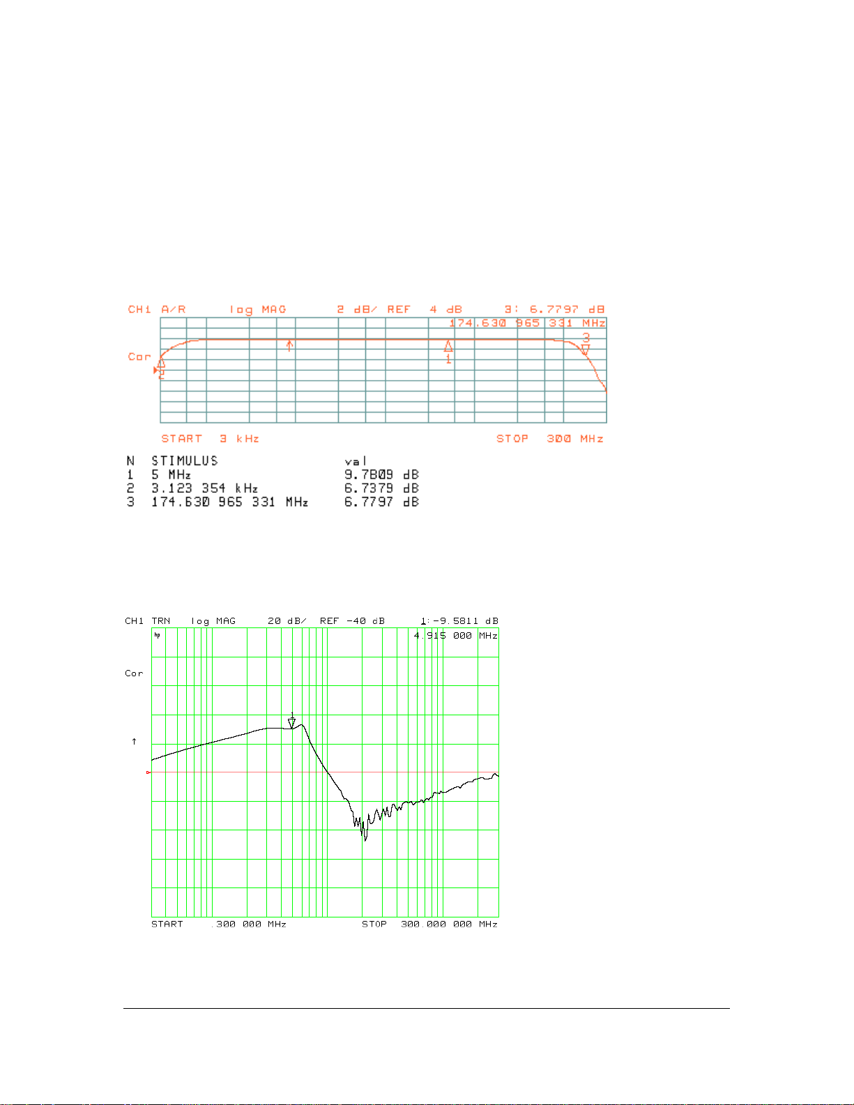
The data presented in this manual was taken with two vector network analyzers; a
Hewlett Packard model 8752B and an HP model 87510A. Both VNAs assume the device
under test is terminated with the network analyzer’s impedance, 50 ohms (The 8752B is a
75 ohm test set and is used with minimum loss 75:50 ohm matching pads for all
measurements presented.) Since the buffer amplifier’s impedance significantly exceeds
50 ohms, a
nearly doubling (+6 dB gain) into a high impedance load. To prevent this effect from
distorting the gain results, all amplifiers under test have their input is terminated with a
49.9 ohm shunt resistor.
At 5 MHz, Unit 1’s measured gain is 9.78 dB, only 0.12 dB less than theoretically predicted.
The 3 dB bandwidth extends from 3 KHz to 174 MHz.
false gain will be observed due to the network analyzer’s output voltage
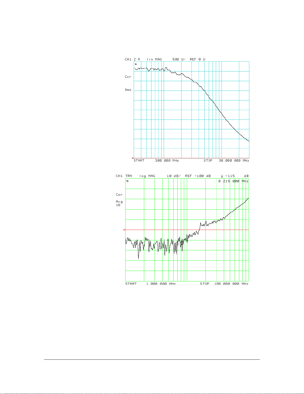
Unit 2, presented below, shows the effect of the K2-specific frequency shaping
components. Both above and below the K2 IF frequency (4.9 MHz), the Z10000-K2’s gain
rolls off. At the desired 4.9 MHz, the net gain is -9.6 dB, necessary to offset the K2’s postmixer ampllifier gain when a net 0 db transfer gain is desired.
Clifton Laboratories – Buffer Amplifier Assembly and Operation Page 3
1.3.2 Input Impedance
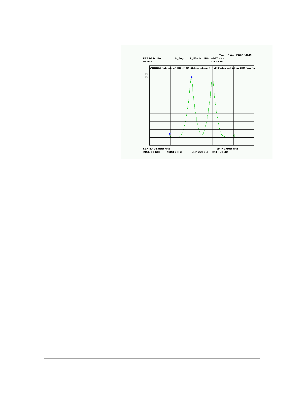
The buffer amplifier’s input
impedance is dominated by
two elements; the bias isolation
resistor (4.7 KΩ in the test
amplifier) and shunt
capacitance (the shunt
capacitance of the PCB
traces, connecting wires to the
amplifier and the amplifier’s
input capacitance.)
The measured data presented
at the right (from Unit 3) should
be considered as
representative of an amplifier
with short (a few inches)
coaxial cable input leads.
1.3.3 Reverse Isolation
The buffer amplifier’s
reverse isolation is a
function of frequency, as
illustrated in the amplifier
measurements presented
at the right for Unit 1. At 8
MHz, the measured sample
exhibited 115 dB reverse
isolation.
Reverse isolation is also
affected by how the
amplifier is housed, lead
dress, shielding, etc.
Accordingly, the isolation
illustrated at the right may
not be achieved in every
instance.
Clifton Laboratories – Buffer Amplifier Assembly and Operation Page 4
1.3.4 Intermodulation Performance
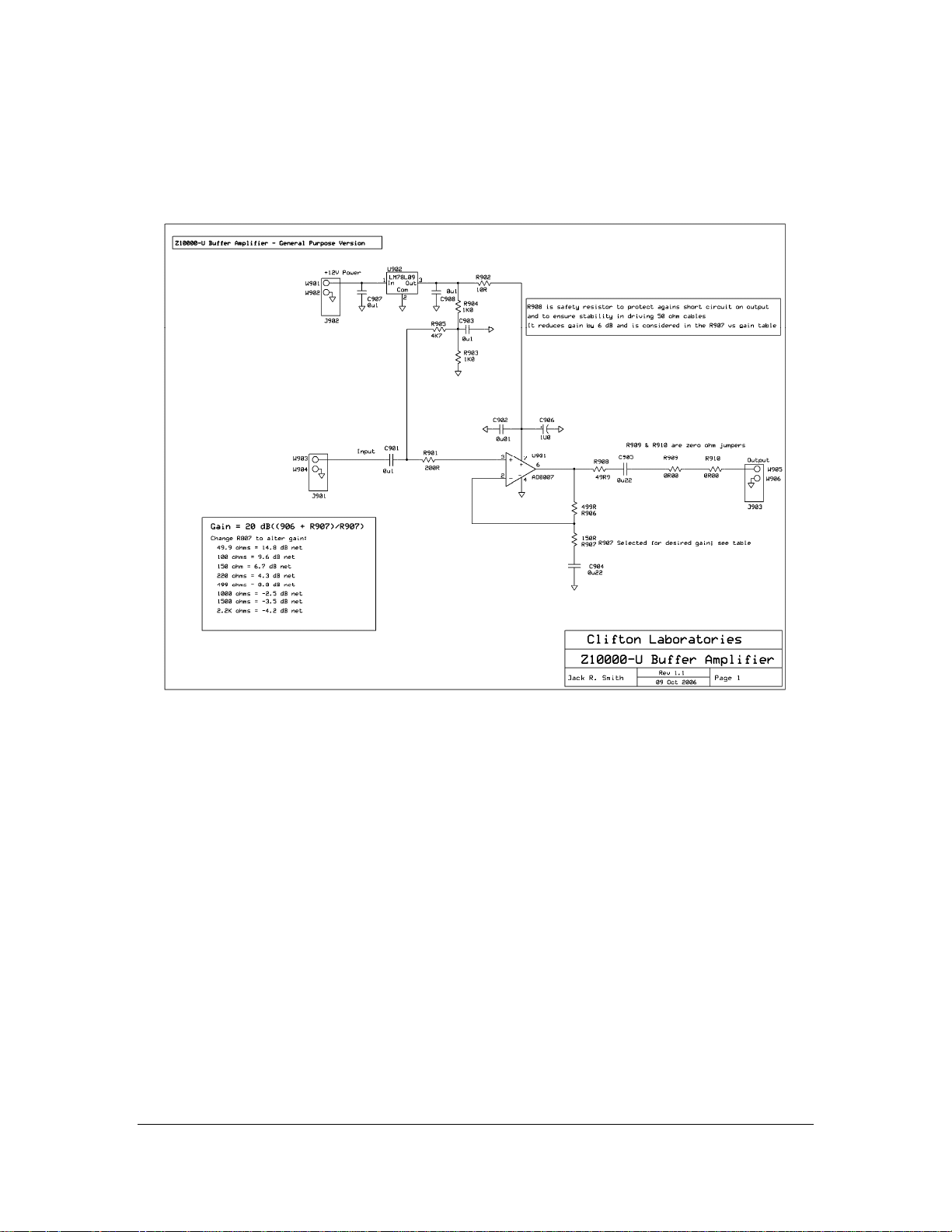
The illustration at the right
shows the output of Unit 1
with two equal signals (9900
KHz and 10100 KHz) of -10
dBm applied to the amplifier
input. The amplifier output is 0
dBm (a 3 dB attenuator is
applied ahead of the
spectrum analyzer in this
plot.)
The third order
intermodulation product is
-71.8 dBm down from either
tone. With an output based
reference, therefore, the IP3
is thus +35.9 dBm.
Clifton Laboratories – Buffer Amplifier Assembly and Operation Page 5
2.0 Schematic and Circuit Description
2.1 Universal Version
Clifton Laboratories – Buffer Amplifier Assembly and Operation Page 6
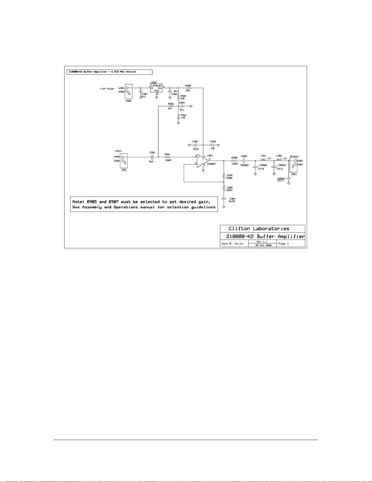
2.2 K2 Version
2.3 Theory of Operation
The operational circuitry of both buffer amplifiers is similar, with differences in component
selection for frequency shaping in the K2 version.
2.3.1 Power Supply.
The AD8007 amplifier is rated at an absolute maximum operating voltage of 12V. In order
to provide a safety margin, and to decouple the amplifier from the power supply, U902,
a three-terminal fixed regulator, provides a source of stable +9V to U901. C907 and C908
provide additional decoupling. U901, the AD8007 amplifier, obtains its power via the RC
decoupling network comprised of R902, C902 and C906.
Since the circuit operates from a single positive power supply, it is necessary to bias
U901’s input to approximately V/2. This is accomplished by the 2:1 voltage divider chain
of R902/R903. C903 bypasses the V/2 reference voltage; whilst R905 increases U901’s
input impedance by isolating C903’s RF ground. R905’s maximum value is determined by
the U901’s input bias current on the positive pin, specified by Analog Devices as 8μA. For
4.7 KΩ, this bias current represents an IR drop of 38 mV. With a DC gain of 4, the
corresponding output DC offset will be about 150 mV. If absolutely necessary for high
input impedance, R905 may be substituted with a higher value resistor, up to
approximately 22 KΩ. However, at frequencies above a few MHz, the input impedance is
Clifton Laboratories – Buffer Amplifier Assembly and Operation Page 7

+
dominated by shunt capacitance; increasing R905 should be done only with an
understanding of all the factors affecting the input impedance.
3
2.3.2 Amplifier
U901, an Analog Devices AD8007, is a high performance, low noise current feedback
amplifier, with a gain-bandwidth product exceeding 650 MHz. A current feedback
amplifier is also known as a “transimpedance” amplifier. Analog Devices describes how
a current feedback amplifier works:
First, the negative input of a CFA responds to current; the output voltage is
proportional to that current, hence transimpedance (V(out) = Z(t) I(in)). Instead of
keeping the negative input current small by maintaining high input impedance,
and using feed-back and voltage gain to keep the input voltage difference
small, the CFA keeps the voltage difference small by virtue of its low input
impedance (like looking back into a low-offset emitter follower); and it keeps its
net input current small dynamically by feedback from the output.
When an ideal CFA is driven at the high-impedance positive input, the negative
input, with its low impedance, follows closely in voltage; and the high gain for
error current and the negative feedback through Rf require that the currents
through Rf and Rin be equal; hence V(out) = V(in)[R(f)/R(in) + 1], just like for
voltage-feedback amplifiers. A major difference is that the slew rate can be quite
high, because large transient currents can flow in the input stage to handle rapid
changes in voltage across the compensating capacitor(s). Also, the low
impedance at the negative input means that stray input capacitance will not
substantially affect the amplifier's bandwidth.
U901’s gain (in dB) is determined by the ratio of resistors R906 and R907:
907906
Gain
In the Z10000-K2 version, R905 and C901 form a high-pass RC filter and input attenuator.
Adjusting R905 to values below 4.7K will increase the input attenuation, which is desirable
to achieve the desired amplifier gain when used in a K2.
The Z1000-K2’s output stage also uses RC high pass filtering (R908 & C905) to roll off
frequencies below approximately 5.6 MHz. The AD8007’s output is connected through a
five element low pass filter, consisting of L901, L902, C910, C911 and C912. The low pass
filter sharply rolls off frequencies above 7 MHz.
C910, C911 and C912 are removed in the Z10000-U model and L901 and L902 are
replaced by zero ohm jumpers. In addition, C901 is changed in the Z10000-U to 0u1 and
C905 to 0u22 to provide a flat frequency response down into the 50 KHz range.
R908, 49.9 Ω, allows U901 to drive capacitive loads, such as coaxial cable and also
protects U901 against operation into short circuits. However, the voltage divider effect of
log20
=
10
R
907
RR
3
Clifton Laboratories will provide interested Z10000 owners with the LTSpice model of the
AD8007 and an LTSpice model of the amplifier circuits upon request. SPICE modeling will allow the
user to determine the effects of component changes with a reasonable degree of accuracy.
Clifton Laboratories – Buffer Amplifier Assembly and Operation Page 8

R908, which is in series with the load, reduces the net available gain into a 50 ohm load
by 6 dB.
2.3.3 Gain Setting in the Z10000-U Buffer Amplifier
Note: This section applies only to the Z10000-U amplifier. See later discussion for gain
setting of the Z10000-K2 amplifier.
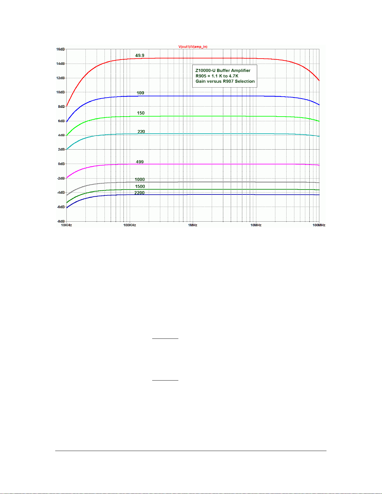
To vary buffer amplifier’s gain, select R907 using the following table or the provided
graph.
Net Gain (net of R908 series resistance) R907
+15 dB 49.9 Ω
+10 dB 100 Ω
+6.7 dB 150 Ω
+4.3 dB 221 Ω
0 dB 499 Ω
-2.5 dB 1000 Ω
-3.5 dB 1500 Ω
-4.2 dB 2200 Ω
R906 and R901 should not be varied from their design values without a thorough analysis
of the circuit.
The effect of changing R907 upon gain and bandwidth is illustrated in the following plot.
The plot is based upon SPICE simulation of the circuit and is representative of the actual
circuit.
In the –U version, R905
will normally be 4K7Ω.
Clifton Laboratories – Buffer Amplifier Assembly and Operation Page 9
If it is necessary to operate the Z10000-U with less than -4.2 dB gain, C901 can be
reduced, or in the event extreme gain reductions are required, R905 may also be
reduced to provide an RC voltage divider at the amplifier’s input. Although this will
introduce some RC frequency shaping in the Z10000-U’s frequency response, the
passband tilt will be insignificant when used with a Z90 panadapter.
Section 4.4.2 of this Manual further discusses gain selection considerations for general
receiver connections.
2.3.4 Gain Setting in the Z10000-K2 Buffer Amplifier
There are two connection point options in the K2. Please read the section of this manual
(page 31) describing the connection point options first, as there are different gain
settings required for the two options.
If you go with connection point Option 1
values:
R905 = 2.2K
R907 = 2.2K
If you go with connection point Option 2
values:
, as a starting point, I recommend the following
as a starting point, I recommend the following
Clifton Laboratories – Buffer Amplifier Assembly and Operation Page 10

R905: 4.7K Ohms
R907: 220 Ohms (this is a starting point; depending on your sound card gain it may be
necessary to reduce R907 to 100 ohms or even 49.9 ohms for increased net gain.)
Note that as the Z10000’s gain is increased, the clipping point of the amplifier decreases.
Larry, N8LP, reports that with R907 at 120 ohms, the clipping point is -5 dBm. Of course, -5
dBm represents an extremely strong signal, unlikely to be encountered in most K2
environments.
If you decide to use connection point Option 1
, gain setting in the K2 version buffer
amplifier is a bit more complex, because the normal operating mode in a K2 transceiver
requires a negative net gain—in other words, a net loss—of about -14 to -15 dB. Part of
4
the negative gain is obtained by intentional rolloff in C901 and R905.
This combination provides a net gain of about -14 dB. This much loss is required because
the recommended K2 connection point has approximately 18 dB net gain from the K2’s
post-mixer amplifier, Q22 (2N5109). The Z90 is designed for optimum signal level when the
5
net gain between the antenna and the Z90’s input is approximately 0 dB.
When
combined with the approximately 3.5 dB loss of the supplied 4.915 MHz bandpass filter,
setting the Z10000-K2’s gain at -14 dB meets the “net zero gain” requirement. (This
computation assumes the K2 is operating in the “normal” mode, i.e., pre-amp off and
attenuation off.) Don’t worry, by the way, about achieving this “net zero gain” objective
perfectly. A few dB one way or the other is not critical. If you are to err, however, better
results will usually be found if you err on the side of operating the Z10000-K2 with a greater
loss than operating it for higher gain.
Although developed with Clifton Laboratories Z90/91 panadapter, measurements shows
that net 0 dB transfer gain (from K2 antenna input to Z10000 sample output) is an
excellent operating point for the Softrock Lite 6.2 receiver when used as a panadapter or
second receiver. If desired, of course, the Z10000’s gain can be increased as discussed
herein.
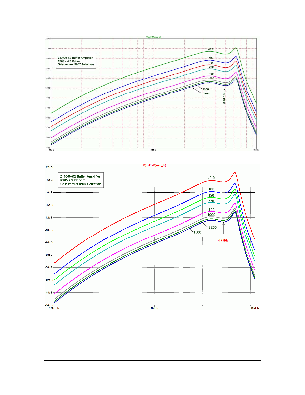
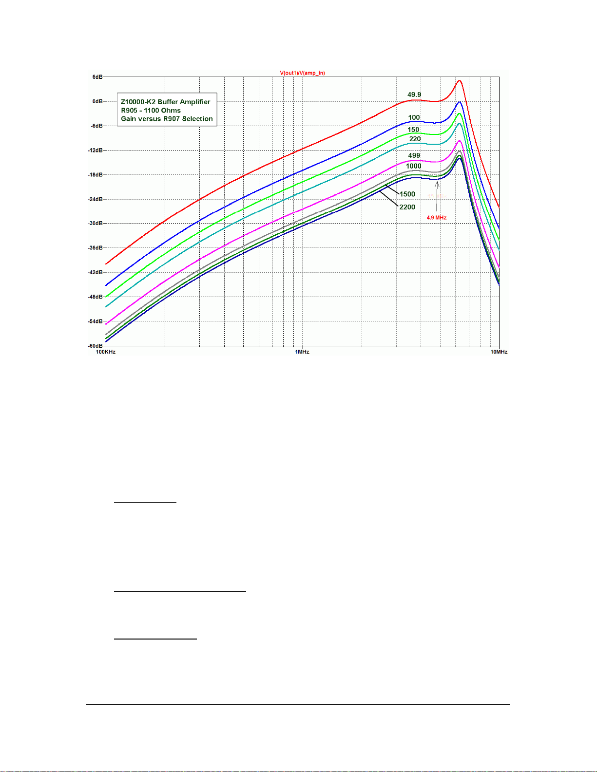
The following three figures show the net gain out of the Z10000-K2 as a function of R907
for three values of R905, 4.7K, 2.2K and 1.1K.
4
It would be possible, of course, to dispense with the buffer amplifier completely and
connect the Z90 to the K2’s IF with a resistive matching pad. However, the resistive matching pad
will not provide isolation as does the Z10000-K2. Although the Z90 has relatively low undesired
emissions from its input connector, the extra isolation of the buffer amplifier provides additional
protection against unwanted signals entering the K2’s IF amplifier chain.
5
In other words, a 1 μV signal at the frequency the receiver it tuned to should yield about a
1 μV signal at 4915 KHz into the Z90.
Clifton Laboratories – Buffer Amplifier Assembly and Operation Page 11
Clifton Laboratories – Buffer Amplifier Assembly and Operation Page 12
3.0 Assembly
3.1 Parts List
The Z10000 parts are packaged in a several small envelopes, depending upon the
option purchased.
All Z10000 kits
• Resistors. All surface mount resistors, for both the –U and –K2 versions. [All R]
• Capacitors for the –U version [All Cap]
• Printed circuit board [PCB]
• Semiconductors (AD8007 and 78L09) [Semi]
K2 Frequency Sensitive Parts
• Capacitors and inductors necessary to shape the amplifier’s frequency
response to peak at 4.9 MHz. [K2 Freq]
:
Internal Mounting
• Parts associated with mounting the Z10000 (either U or K2) inside a receiver. [Int]
• K2-specific internal connectors are supplied where the purchaser selects the
Internal Mounting option and also the K2 frequency sensitive parts. [K2 Con]
Clifton Laboratories – Buffer Amplifier Assembly and Operation Page 13
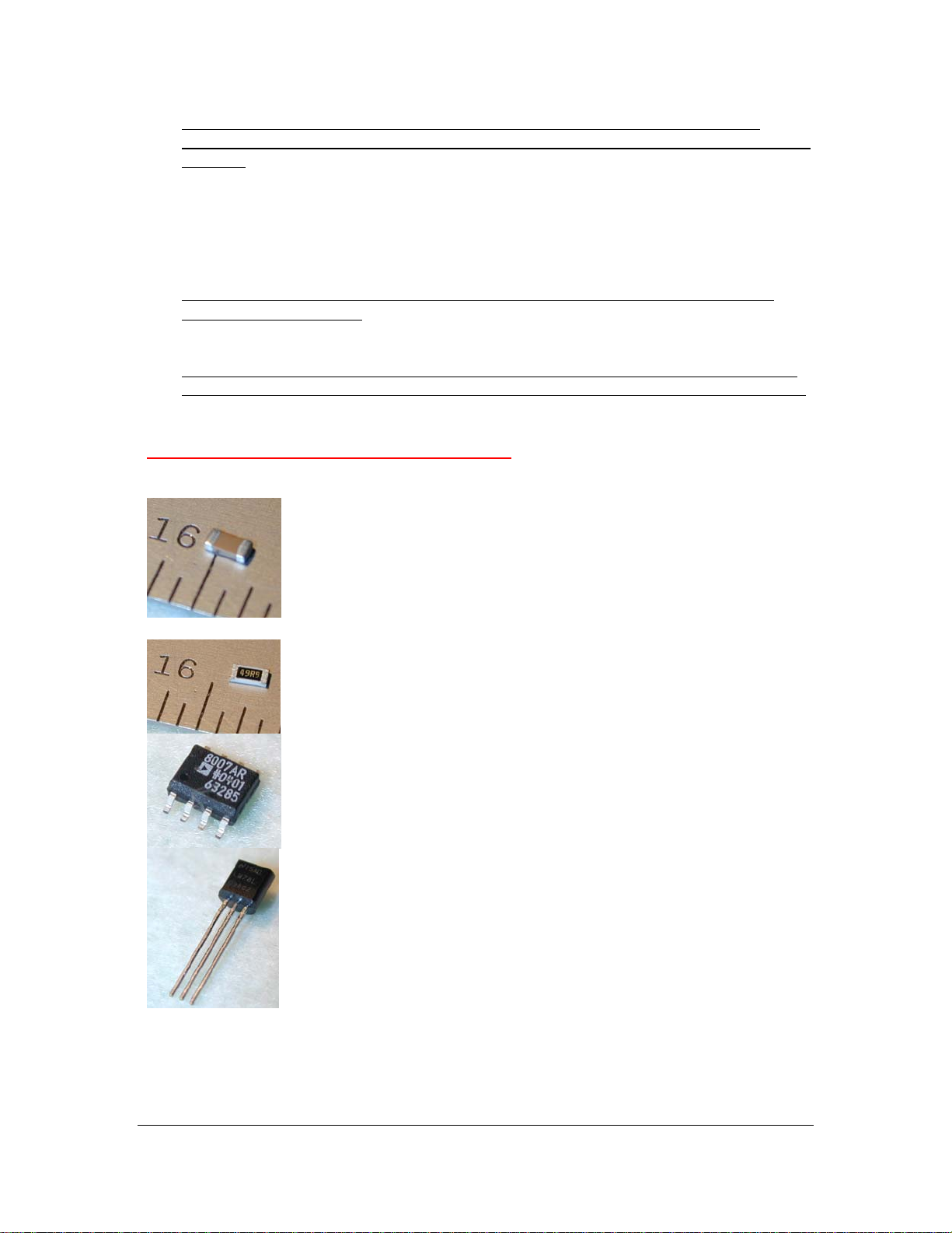
If ordering a Z10000-K2, therefore, you will have several extra capacitors and
resistors that are not used in the –K2 version, as all kits are shipped with the full set of
–U parts.
When working with capacitors particularly, do not removed the individual parts
from their color-coded packaging until you are ready to use the component, as
their values are not marked on the part and cannot normally be visually
distinguished. Hence, if you mix up the capacitors, you will have to measure their
values with a capacitance meter.
Also, do not confuse 100 ohm 1% resistors (identified as 1000) with 1.0K ohm 1%
parts, identified as 1001.
Note that the schematic identifies parts with the multiplier as the “decimal” point.
For example a 1K ohm resistor is identified as a 1K0, and a 49.9 ohm resistor as 49R9.
Common Components - K2 and Universal Models
Envelope
Typical Photo Designation Value Marking Number Qty
C902 0u01 Not marked All Cap 1
C903 0u1 Not marked All Cap 1
C904 0u22 Not marked All Cap 1
C906 1u0 Not marked All Cap 1
C907 0u1 Not marked All Cap 1
C908 0u1 Not marked All Cap 1
R901 200R 2000 All R 1
R902 10R 10R0 All R 1
R903 1K0 1001 All R 1
R904 1K0 1001 All R 1
R906 499R 4990 All R 1
R908 49R9 49R9 All R 1
U901 AD8007 AD8007ARZ Semi 1
U902 LM78L09 KA78L09AZ Semi 1
Clifton Laboratories – Buffer Amplifier Assembly and Operation Page 14
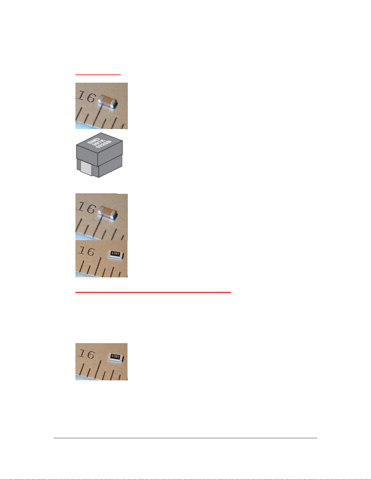
Envelope
Typical Photo Designation Value Marking Number Qty
Z10000-K2 Only
Z10000-U Only
C901 8p2 Not marked K2 Freq 1
C905 5600pF Not marked K2 Freq 1
C910 1200pF Not marked K2 Freq 1
C911 1200pF Not marked K2 Freq 1
C912 1200pF Not marked K2 Freq 1
L901 1u5 K2 Freq 1
L902 1u5 K2 Freq 1
C901 0u1 Not marked All Cap 1
C905 0u22 Not marked All Cap 1
L901 0 ohm jumper All R
L902 0 ohm jumper All R
Gain Setting Parts - For both Z10000-K2 and Z10000-U
See manual to determine proper value
Resistor Supplied for Selection
R905 4K7 4701 All R 1
R905 2K2 2201 All R 1
R905 1K1 1101 All R 1
Resistor Supplied for Selection
R907 49R9 49R9 All R 1
R907 100R 1000 All R 1
R907 150R 1500 All R 1
R907 220R 2200 All R 1
R907 499R 4990 All R 1
R907 1K0 1001 All R 1
R907 1K5 1501 All R 1
R907 2K2 2201 All R 1
External and Mechanical Parts
Clifton Laboratories – Buffer Amplifier Assembly and Operation Page 15
Both Z10000-K2 and Z10000-U
Z10000-01 RG178 2 ft INT
Z10000-02 Bulkhead Connector INT
Z10000-03 6" red wire INT
Z10000-04 1/2" MF 4-40 standoff INT
Z10000-12 fish paper INT
Z10000-08 Printed circuit board
Z10000-10 4-40x1/4" machine screw INT
Z10000-11 4-40 hex nut INT
Z10000-12 3/32" x .5" red heat shrink tubing INT
Z10000-13 3/32" x .5" black heat shrink tubing INT
Z10000-14 3/32" x .5 green heat shrink tubing INT
Z10000-16 3/16" x 2" heat shrink tubing INT
Z10000-K2 Only
Z10000-05 8-pin female header All R
Z10000-06 3-pin female header All R
Z10000-07 3-pin male header All R
Multiple part values are provided for R905 and R907, to be selected by the builder as
discussed in the text.
Printed instructions are not supplied; this manual is to be downloaded from the Clifton
Laboratories web site.
Heat shrink tubing supplied may differ in diameter, length and color from the values in
the above parts table.
3.2 Working with Surface Mount Components
If you are unfamiliar with installing surface mount components, you should review this
section of the Assembly Manual. The surface mount components in this kit are
considered “large” by industry standards, and should not represent difficulty if you have
prior kit assembly experience, either surface mount or through-hole.
3.2.1 Tools
I use the following tools in assembling surface mount printed circuit boards:
Tool Comments Approximate
Cost
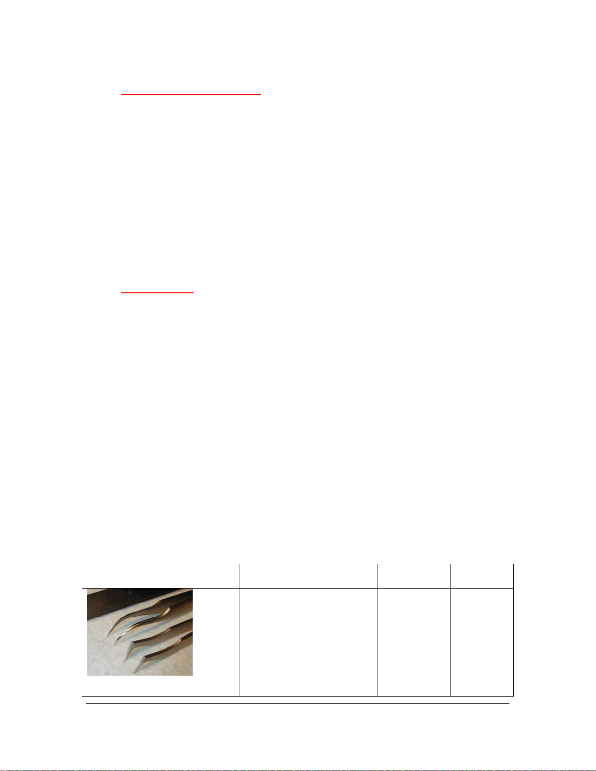
I use curved nose forceps
to hold parts while
soldering. I prefer the
pattern 7-SA forceps with
gently curved tips, but the
angular pattern 6-SA may
be preferred by some.
These are by Technik and
are non-magnetic stainless
$9.00 each MSC part
Source
number:
7-SA
pattern:
88348099
6-SA
pattern:
88348081
Clifton Laboratories – Buffer Amplifier Assembly and Operation Page 16
 Loading...