Pozosta DR-135, DR-235, DR-435 User Manual

DR-135 / DR-235 / DR-435
Downloaded by
RadioAmateur.EU
Service Manual
CONTENTS
SPECIFICATIONS
GENERAL ........................................................................................ 2
TRANSMITTER ................................................................................ 2
RECEIVER ....................................................................................... 2
CIRCUIT DESCRIPTION DR-135
1) Receiver System (DR-135)........................................................... 3, 4
2) Transmitter System (DR-135) ....................................................... 4, 5
3) PLL Synthesizer Circuit (DR-135) ................................................. 5, 6
4) Receiver System (DR-235)........................................................... 6, 7
5) Transmitter System (DR-235) ....................................................... 7, 8
6) PLL Synthesizer Circuit (DR-235) ................................................. 8, 9
7) Receiver System (DR-435)......................................................... 9, 10
8) Transmitter System (DR-435) ......................................................... 10
9) PLL Synthesizer Circuit (DR-435) ................................................... 11
10) CPU and Peripheral Circuits(DR-135 DR-235 DR-435) ............. 11,12
11) Power Supply Circuit....................................................................... 13
12) M3826M8269GP (XA0818)....................................................... 14~16
SEMICONDUCTOR D AT A
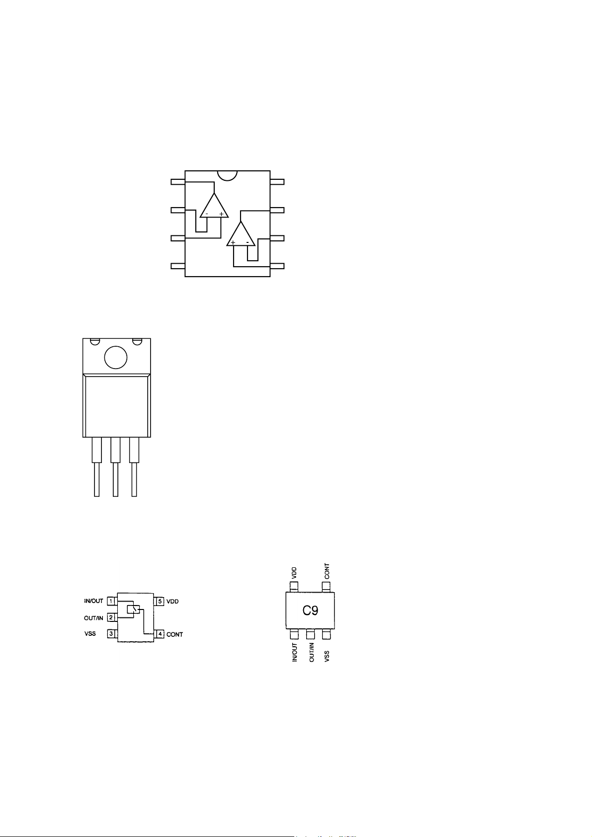
1) M5218FP (XA0068) ........................................................................ 17
2) NJM7808FA (XA0102).................................................................... 17
3) TC4S66F (XA0115) ........................................................................ 17
4) TK10930VTL (XA0223) .................................................................. 18
5) BU4052BF (XA0236) ...................................................................... 19
6) TC4W53FU (XA0348) .................................................................... 19
7) M64076GP (XA0352) ..................................................................... 20
8) LA4425A (XA0410)......................................................................... 21
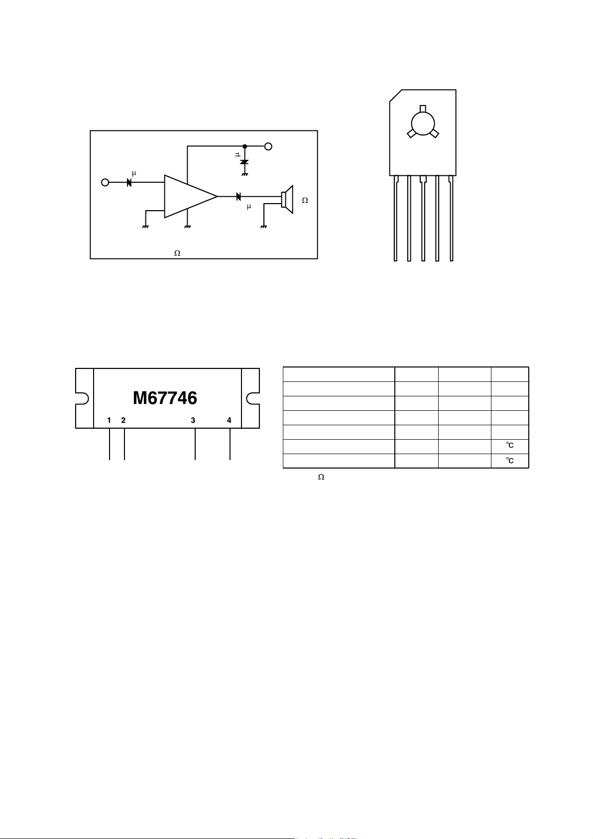
9) M67746 (XA0412) .......................................................................... 21
10) M68729 (XA0591) .......................................................................... 22
11) M57788 (XA0077A) ........................................................................ 23
12) mPC2710T (XA0449) ..................................................................... 24
13) NJM2902 (XA0596) ........................................................................ 24
14) 24LC32A (XA0604) ........................................................................ 25
15) S-80845ALMP-EA9-T2 (XA0620) ................................................... 25
16) L88MS05TLL (XA0675) .................................................................. 25
17) AN8010M (XA0119) ....................................................................... 26
18) TK10489M (XA0314) ...................................................................... 26
19) T ransistor , Diode , and LED Ontline Dr awings .................................. 27
20) LCD Connection (TTR3626UPFDHN) ........................................... 28
EXPLODED VIEW
1) T op and Front View ......................................................................... 29
2) Bottom View.................................................................................... 30
3) LCD Assembly................................................................................ 31
PAR TS LIST
CPU ..........................................................................................32, 33
Main Unit(DR-135).................................................................... 33~36
Main Unit(DR-235).................................................................... 36~39
VCO Unit(DR-235) ......................................................................... 39
Main Unit(DR-435).......................................................................... 42
VCO Unit(DR-435) ......................................................................... 42
Mechanical Parts ............................................................................ 43
Packing P arts ................................................................................. 43
ACCESSORIES.............................................................................. 43
ACCESSORIES(SCREW SET) ...................................................... 43
TNC(EJ41U) .................................................................................. 44
TNC (EJ41U) Packing Parts ........................................................... 45
DR-135 ADJUSTMENT
1) Adjustment Spot ............................................................................ 46
2) VCO and RX Adjustment Specification ........................................... 47
3) Tx Adjustment Specification ............................................................ 47
4) Rx T est Specification ....................................................................... 48
5) Tx Test Specification ....................................................................... 49
DR-235 ADJUSTMENT
1) Adjustment Spot ............................................................................ 50
2) VCO and RX Adjustment Specification ........................................... 51
3) Tx Adjustment Specification ............................................................ 51
4) Rx T est Specification ....................................................................... 52
5) Tx Test Specification ....................................................................... 53
DR-435 ADJUSTMENT
1) Adjustment Spot ............................................................................ 54
2) VCO and RX Adjustment Specification ........................................... 55
3) Tx Adjustment Specification ............................................................ 55
4) Rx T est Specification ....................................................................... 56
5) Tx Test Specification ....................................................................... 57
PC BOARD VIEW
1) CPU Unit Side A ............................................................................. 58
2) CPU Unit Side B ............................................................................. 58
3) Main Unit Side A DR-135 (UP 0400B) ............................................. 59
4) Main Unit Side B DR-135 (UP 0400B) ............................................. 59
5) Main Unit Side A DR-235 (UP 0414) ............................................... 60
6) Main Unit Side B DR-235 (UP 0414) ............................................... 60
7) Main Unit Side A DR-435 (UP 0415) ............................................... 61
8) Main Unit Side B DR-435 (UP 0415) ............................................... 61
9) Tnc Unit Side A (UP 0402) (DR-135TP only) .................................. 62
10) Tnc Unit Side B (UP 0402) (DR-135TP only) .................................. 62
SCHEMATIC DIA GRAM
1) CPU Unit DR-135 / DR-235 / DR-435 ............................................. 63
2) Main Unit DR-135 ........................................................................... 64
3) Main Unit DR-235 ........................................................................... 65
4) Main Unit DR-435 ........................................................................... 66
5) TNC Unit (DR-135TP only) ............................................................. 67
BLOCK DIAGRAM
1) DR-135........................................................................................... 68
2) DR-235........................................................................................... 69
3) DR-435........................................................................................... 70
ALINCO,INC.
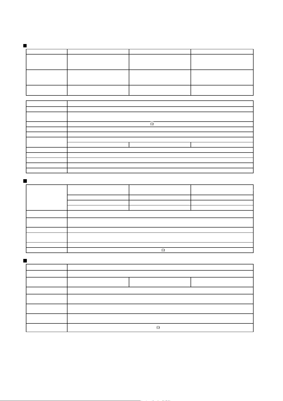
SPECIFICATIONS
Downloaded by
RadioAmateur.EU
General
Frequency coverage DR-135 DR-235 DR-435
T,TG
(U.S amateur)
E,EG
(European amateur)
TA,TAG 118.000 ~ 135.995MHz (AM RX)
(Commercial) 136.000 ~ 173.995MHz (RX.TX)
118.000 ~ 135.995MHz (AM RX) 216.000 ~ 279.995MHz (RX) 350.000 ~ 511.995MHz (RX)
136.000 ~ 173.995MHz (RX) 222.000 ~ 224.995MHz (TX) 430.000 ~ 449.995MHz (TX)
144.000 ~ 147.995MHz (TX)
144.000 ~ 145.995MHz (RX.TX) 430.000 ~ 439.995MHz (RX.TX)
Operating mode
Frequency resolution
Number of memory
channels
Antenna impedance
Power requirement
Ground method
Current drain Receive 0.6A(Max.) 0.4A(Squelched)
Transmit 11.0A max. 8.0A max. 10.0A max.
Operating temperature
Frequency stability
Dimensions
Weight
FM 16K0F3E (Wide mode) 8K50F3E (Narrow mode)
5,8.33,10,12.5,15,20,25,30,50 KHz
100
50 unbalanced
13.8V DC ±15% (11.7 to 15.8V)
Negative ground
˚C ˚C
- 10 to 60
±5ppm
142(w)×40(h)×174(d) mm
( 142×40×188mm for projection included)
Approx. 1.0kg
Transmitter
Output power High:50W (144-148MHz) High:25W High:35W
More than 33W (136-174MHz)
Mid:10W Mid:10W Mid:10W
Low:Approx.5W Low:Approx.5W Low:Approx.5W
Modulation system
Maximum frequency
deviation
Spurious emission
Adjacent
channel power
Noise and hum ratio
Microphone impedance
Variable reactance frequency modulation
±5kHz (Wide mode) ±2.5kHz (Narrow mode)
-60dB
-60dB
-40dB (Wide mode) -34dB (Narrow mode)
2k
Receiver
Sensitivity
Receiver circuitry
Intermediate
frequency
Squelch sensitivity
Adjacent channel
selectivity
Intermoduration
rejection ratio
Spurious and
image rejection ratio
Audio output power
2
-16dBu for 12dB SINAD
Double conversion superheterodyne
1st 21.7MHz 2nd 450kHz 1st 30.85MHz 2nd 455kHz 1st 30.85MHz 2nd 455kHz
-18dBu
-65dB(Wide mode) -55dB(Narrow mode)
60dB
70dB
2.0W (8 ,10%THD)
! Note: All specifications are subject to change without notice or obligation.

CIRCUIT DESCRIPTION DR-135/DR-235/DR-435
1) Receiver System (DR-135)
The receiver system is a double superheterodyne system with a 21.7 MHz first IF and a 450 kHz second IF.
1. Fr ont End
The received signal at an y frequency in the 136.000MHz to 173.995MHz range
is passed through the low-pass filter (L116, L115, L114, L113, C204, C203,
C202, C216 and C215) and tuning circuit (L105, L104 and D105, D104), and
amplified by the RF amplifier (Q107). The signal from Q107 is then passed
through the tuning circuit (L103, L102, and varicaps D103 and D102) and
converted into 21.7 MHz by the mixer (Q106). The tuning circuit, which
consists of L105, L104, varicaps D105 and D104, L103, L102, varicaps
D103 and D102, is controlled by the tracking v oltage form the VCO . The local signal
from the VCO is passed through the b uff er (IC112), and supplied to the source of
the mixer (Q106). The radio uses the low er side of the superheterodyne system.
2. IF Circuit
The mixer mixes the receiv ed signal with the local signal to obtain the sum of
and difference between them. The crystal filter (XF102, XF101) selects 21.7
MHz frequency from the results and eliminates the signals of the unwanted
frequencies. The first IF amplifier (Q105) then amplifies the signal of the selected
frequency .
3. Demodulator Cir cuit
4. A udio Cir cuit
After the signal is amplified by the first IF amplifier (Q105), it is input to pin 24 of
the demodulator IC (IC108). The second local signal of 21.25 MHz (shared
with PLL IC reference oscillation), which is oscillated by the internal oscillation
circuit in IC116 and crystal (X103), is input through pin 1 of IC108. Then, these
two signals are mixed by the internal mix er in IC108 and the result is conv erted
into the second IF signal with a frequency of 450 kHz. The second IF signal is
output from pin 3 of IC108 to the ceramic filter (FL101 or FL102), where the
unwanted frequency band of that signal is eliminated, and the resulting signal
is sent back to the IC108 through pins 5.
The second IF signal input via pin 5 is demodulated by the internal limiter
amplifier and quadrature detection circuit in IC108, and output as an audio
signal through pin 12.
The audio signal from pin 12 of IC108 is amplified by the audio amplifier
(IC104:A),and switched by the signal switch IC (IC111) and then input it to the
de-emphasis circuit.
and is compensated to the audio frequency characteristics in the de-emphasis
circuit (R203, R207, R213, R209, C191, C218, C217) and amplified by the AF
amplifier (IC104:D). The signal is then input to v olume (VR1) . The adjusted signal is
sent to the audio power amplifier (IC117) through pin 1 to drive the speaker .
3

5. Squelch Circuit
The detected output which is outputted from the pin 12 of IC108 is inputted to
pin 19 of IC108 after it was been amplified by IC104:A and it is outputted from
pin 20 after the noise component was been eliminated from the composed
band pass filter in the built in amplifier of the IC, then the signal is rectified b y
D106 to convert into DC component. The adjusted voltage level at VR101 is
delivered to the comparator of the CPU.
The voltage is led to pin 2 of CPU and compared with the setting voltage . The
squelch will open if the input voltage is lower than the setting voltage.
During open squelch, pin 30 (SQC) of the CPU becomes "L" level, AF control
signal is being controlled and sounds is outputted from the speaker .)
6. AIR Band Reception(T onl y)
When the frequency is within 118~135.995MHz, Q110 automatically turns ON,
pin 14 of IC108 becomes "L" level and the condition becomes in AM detection
mode.
The receiver signal passed through the duplexer is let to the antenna switch
(D107,D101). After passing through the band-pass filter, the signal is amplified
by RF amplifier Q112. Secondly the signal is mixed with the signal from the first
local oscillator in the first-mixer Q106,then conv erted into the first IF. Its unwanted
signal is let to IC106, pin24. Then conv erted into the second IF . and is demodulated
by AM decoder of IC106, and is output from pin13 as the AF signal.
7. WIDE/NARRO W switching circuit
The 2nd IF 450 kHz signal which passes through filter FL101 (wide) and FL102
(narrow) during narrow, changes its width using the width control switching
IC103 and IC102.
2) Transmitter System (DR-135)
1. Modulator Cir cuit
The audio signal is converted to an electrical signal by the microphone, and
input it to the microphone amplifier (Q6). Amplified signal which passes through
mic-mute control IC109 is adjusted to an appropriate mic-volume b y means of
mic-gain adjust VR106.
IC114:A and B consists of two operational amplifiers; one amplifier (pins 1, 2,
and 3) is composed of pre-emphasis and IDC circuits and the other (pins 5, 6,
and 7) is composed of a splatter filter. The maximum frequency deviation is
obtained by VR107. and input to the signal switch (IC113) (9600 bps packet
signal input switch) and input to the cathode of the varicap of the VCO, to
change the electric capacity in the oscillation circuit. This produces the frequency
modulation.
4

2. Power Amplifier Circuit
The transmitted signal is oscillated by the VCO , amplified by the driv e amplifier
(IC112) and younger amplifier (Q115), and input to the final power module
(IC110). The signal is then amplified by the final pow er module (IC110) and led
to the antenna switch (D110) and low-pass filter (L113, L114, L115, L116,
C215, C216, C202, C203 and C204), where unwanted high harmonic wav es
are reduced as needed, and the resulting signal is supplied to the antenna.
3. APC Cir cuit
Part of the transmission power from the low-pass filter is detected b y D111 and
D112, converted to DC. The detection v oltage i s passed through the APC circuit
(Q118, Q117, Q116), then it controls the APC voltage supplied to the younger
amplifier Q115 and the final power module IC110 to fix the transmission pow er.
3) PLL Synthesizer Circuit (DR-135)
1. PLL
The dividing ratio is obtained by sending data from the CPU (IC1) to pin 2 and
sending clock pulses to pin 3 of the PLL IC (IC116). The oscillated signal from
the VCO is amplified by the buffer (Q134 and Q135) and input to pin 15 of
IC116. Each programmable divider in IC116 divides the frequency of the input
signal by N according to the frequency data, to generate a comparison frequency of
5 or 6.25 kHz.
2. Reference Frequency Circuit
The reference frequency appropriate for the channel steps is obtained b y dividing
the 21.25 MHz reference oscillation (X103) b y 4250 or 3400, according to the data
from the CPU (IC1). When the resulting frequency is 5 kHz, channel steps of 5,
10, 15, 20, 25, 30, and 50 kHz are used. When it is 6.25 kHz, the 12.5 kHz
channel step is used.
3. Phase Comparator Circuit
The PLL (IC116) uses the reference frequency, 5 or 6.25kHz. The phase
comparator in the IC116 compares the phase of the frequency from the VCO
with that of the comparison frequency, 5 or 6.25kHz, which is obtained by the
internal divider in IC116.
4. PLL Loop Filter Cir cuit
If a phase difference is f ound in the phase comparison between the ref erence
frequency and VCO output frequency, the charge pump output (pin 13) of IC116
generates a pulse signal, which is converted to DC voltage by the PLL loop
filter and input to the varicap of the VCO unit for oscillation frequency control.
5

5. VCO Circuit
A Colpitts oscillation circuit driven by Q131 directly oscillates the desired frequency.
The frequency control voltage determined in the CPU (IC1) and PLL circuit is
input to the varicaps (D122 and D123). This change the oscillation frequency,
which is amplified by the VCO b uff er (Q134) and output from the VCO area.
6. VCO Shift Circuit
During transmission or the AIR band Reception (118~136 MHz), the VCO shift
circuit turns ON Q138, change control the capacitance of L123 and safely
oscillates the VCO b y means of H signal from pin 16 of IC116.)
4) Receiver System (DR-235)
The receiver system is a double superheterodyne system with a 30.85 MHz first IF and a 455 kHz second IF.
1. Front End
The received signal at an y frequency in the 216.000MHz to 279.995MHz range
is passed through the low-pass filter (L116, L115, L114, L113, C204, C203,
C202, C216 and C215) and tuning circuit (L105, L104 and D105, D104), and
amplified by the RF amplifier (Q107). The signal from Q107 is then passed
through the tuning circuit (L103, L107, L102, and varicaps D103, D107 and
D102) and converted into 30.85 MHz by the mixer (Q106). The tuning circuit,
which consists of L105, L104, varicaps D105 and D104, L103, L107, L102,
varicaps D103, D107 and D102, is controlled by the tracking voltage form the
VCO. The local signal from the VCO is passed through the b uff er (Q112), and
supplied to the source of the mixer (Q106). The radio uses the lower side of the
superheterodyne system.
2. IF Circuit
3. Demodulator Cir cuit
The mixer mixes the receiv ed signal with the local signal to obtain the sum of
and difference between them. The crystal filter (XF102, XF101) selects 30.85
MHz frequency from the results and eliminates the signals of the unwanted
frequencies. The first IF amplifier (Q105) then amplifies the signal of the selected
frequency .
After the signal is amplified by the first IF amplifier (Q105), it is input to pin 24 of
the demodulator IC (IC108). The second local signal of 30.395 MHz, which is
oscillated by the internal oscillation circuit in IC108 and crystal (X104), is input
through pin 1 of IC108. Then, these two signals are mix ed by the internal mixer
in IC108 and the result is converted into the second IF signal with a frequency
of 455 kHz. The second IF signal is output from pin 3 of IC108 to the ceramic
filter (FL101 or FL102), where the unwanted frequency band of that signal is
eliminated, and the resulting signal is sent back to the IC108 through pins 5.
The second IF signal input via pin 5 is demodulated by the internal limiter
amplifier and quadrature detection circuit in IC108, and output as an audio
signal through pin 12.
6

4. A udio Cir cuit
5. Squelch Circuit
The audio signal from pin 12 of IC108 is amplified by the audio amplifier
(IC104:A), and switched b y the signal switch IC (IC111) and then input it to the
de-emphasis circuit.
and is compensated to the audio frequency characteristics in the de-emphasis
circuit (R203, R207, R213, R209, C191, C218, C217) and amplified by the AF
amplifier (IC104:D). The signal is then input to volume (VR1) . The adjusted
signal is sent to the audio power amplifier (IC117) through pin 1 to drive the
speaker .
The detected output which is outputted from the pin 12 of IC108 is inputted to
pin 19 of IC108 after it was been amplified by IC104:A and it is outputted from
pin 20 after the noise component was been eliminated from the composed
band pass filter in the built in amplifier of the IC, then the signal is rectified b y
D106 to convert into DC component. The adjusted voltage level at VR101 is
delivered to the comparator of the CPU.
The voltage is led to pin 2 of CPU and compared with the setting voltage . The
squelch will open if the input voltage is lower than the setting voltage.
During open squelch, pin 30 (SQC) of the CPU becomes "L" level, AF control
signal is being controlled and sounds is outputted from the speaker .)
6. AIR Band Reception(T onl y)
If it is made air band receiving mode, IF signal is demodulated by AM decoder
of IC106, and is output from pin13 as the AF signal.
7. WIDE/NARRO W switching circuit
The 2nd IF 455 kHz signal which passes through filter FL101 (wide) and FL102
(narrow) during narrow, changes its width using the width control switching
IC103 and IC102.
5) Transmitter System (DR-235)
1. Modulator Cir cuit
The audio signal is converted to an electrical signal by the microphone, and
input it to the microphone amplifier (Q6). Amplified signal which passes through
mic-mute control IC109 is adjusted to an appropriate mic-volume b y means of
mic-gain adjust VR106.
IC114:A and B consists of two operational amplifiers; one amplifier (pins 1, 2,
and 3) is composed of pre-emphasis and IDC circuits and the other (pins 5, 6,
and 7) is composed of a splatter filter. The maximum frequency deviation is
obtained by VR107. and input to the signal switch (IC113) (9600 bps packet
signal input switch) and input to the cathode of the varicap of the VCO, to
change the electric capacity in the oscillation circuit. This produces the frequency
modulation.
7

2. P ower Amplifier Circuit
The transmitted signal is oscillated by the VCO , amplified by the driv e amplifier
(IC112) and younger amplifier (Q115), and input to the final power module
(IC110). The signal is then amplified by the final pow er module (IC110) and led
to the antenna switch (D110) and low-pass filter (L113, L114, L115, L116,
C215, C216, C202, C203 and C204), where unwanted high harmonic wav es
are reduced as needed, and the resulting signal is supplied to the antenna.
3. APC Cir cuit
Part of the transmission power from the low-pass filter is detected by D111
and D112, converted to DC. The detection voltage is passed through the
APC circuit (Q118, Q117, Q116), then it controls the APC voltage supplied to
the younger amplifier Q115 and the final power module IC110 to fix the
transmission power.
6) PLL Synthesizer Circuit (DR-235)
1. PLL
The dividing ratio is obtained by sending data from the CPU (IC1) to pin 2 and
sending clock pulses to pin 3 of the PLL IC (IC501). The oscillated signal from
the VCO is amplified by the buffer (Q504 and Q501) and input to pin 15 of
IC501. Each programmable divider in IC501 divides the frequency of the input
signal by N according to the frequency data, to generate a comparison frequency of
5 or 6.25 kHz.
2. Reference Frequency Circuit
The reference frequency appropriate for the channel steps is obtained by
dividing the 12.8 MHz ref erence oscillation (X103) b y 2560 or 2048, according
to the data from the CPU (IC1). When the resulting frequency is 5 kHz, channel
steps of 5, 10, 15, 20, 25, 30, and 50 kHz are used. When it is 6.25 kHz, the
12.5 kHz channel step is used.
3. Phase Comparator Circuit
The PLL (IC501) uses the reference frequency, 5 or 6.25kHz. The phase
comparator i n the IC501 compares the phase of the frequency from the VCO
with that of the comparison frequency, 5 or 6.25kHz, which is obtained by the
internal divider in IC501.
4. PLL Loop Filter Cir cuit
If a phase difference is f ound in the phase comparison between the ref erence
frequency and VCO output frequency, the charge pump output (pin 13) of IC501
generates a pulse signal, which is converted to DC voltage by the PLL loop
filter and input to the varicap of the VCO unit for oscillation frequency control.
8

5. VCO Circuit
A Colpitts oscillation circuit driven by Q503 directly oscillates the desired frequency .
The frequency control voltage determined in the CPU (IC1) and PLL circuit is
input to the varicaps (D503 and D504). This change the oscillation frequency,
which is amplified by the VCO b uff er (Q504) and output from the VCO area.
7) Receiver System (DR-435)
The receiver system is a double superheterodyne system with a 30.85 MHz first IF and a 455 kHz second IF.
1. Fr ont End
The received signal at any frequency in the 430.00MHz to 439.995MHz range
is passed through the low-pass filter (L115, L114, L116, C204, C203, C202,
C216 and C215) and amplified by the RF amplifier (Q107). The signal from
Q107 is then passed through the BPF circuit (L103, L102) and converted into
30.85 MHz by the mixer (Q106). The local signal from the VCO is passed
through the buffer (Q503,Q504), and supplied to the source of the mix er (Q106).
The radio uses the lower side of the superheterodyne system.
2. IF Circuit
The mixer mixes the receiv ed signal with the local signal to obtain the sum of
and difference between them. The crystal filter (XF101) selects 30.85MHz frequency
from the results and eliminates the signals of the unwanted frequencies. The first IF
amplifier (Q105) then amplifies the signal of the selected frequency.
3. Demodulator Cir cuit
4. A udio Cir cuit
After the signal is amplified by the first IF amplifier (Q105), it is input to pin 20 of
the demodulator IC (IC108). The second local signal of 30.85MHz (Crystal
oscillator) is input pin 1 of IC108. Then, these two signals are mixed by the
internal mixer in IC108 and the result is converted into the second IF signal
with a frequency of 455 kHz. The second IF signal is output from pin 4 of IC108
to the ceramic filter (FL101 or FL102), where the unwanted frequency band of
that signal is eliminated, and the resulting signal is sent back to the IC108
through pins 6.
The second IF signal input via pin 6 is demodulated by the internal limiter
amplifier and quadrature detection circuit in IC108, and output as an audio
signal through pin 11.
The audio signal from pin 11 of IC108 is amplified by the audio amplifier
(IC104:A), and switched b y the signal switch IC (IC111) and then input it to the
de-emphasis circuit.
and is compensated to the audio frequency characteristics in the de-emphasis
circuit (R203, R207, R213, R209, C191, C218, C217) and amplified by the AF
amplifier (IC104:D). The signal is then input to volume (VR1) . The adjusted
signal is sent to the audio power amplifier (IC117) through pin 1 to drive the
speaker .
9

5. Squelch Circuit
The detected output which is outputted from the pin 11 of IC108 is inputted to
pin 13 of IC108 after it was been amplified by IC104:A and it is outputted from
pin 14 after the noise component was been eliminated from the composed
band pass filter in the built in amplifier of the IC, then the signal is rectified b y
D106 to convert into DC component. The adjusted voltage level at VR101 is
delivered to the comparator of the CPU.
The v oltage is led to pin 2 of CPU and compared with the setting v oltage. The
squelch will open if the input voltage is lower than the setting voltage.
During open squelch, pin 30 (SQC) of the CPU becomes "L" level, AF control
signal is being controlled and sounds is outputted from the speaker.
6. WIDE/NARRO W switching circuit
The 2nd IF 455 KHz signal which passes through filter FL101 (wide) and FL102
(narrow) during narrow, changes its width using the width control switching
IC103 and IC102.
8) Transmitter System (DR-435)
1. Modulator Cir cuit
The audio signal is converted to an electrical signal by the microphone, and
input it to the microphone amplifier (Q6). Amplified signal which passes through
mic. mute control IC109 is adjusted to an appropriate mic. volume b y means of
mic. gain adjust VR106.
IC114:A and B consists of two operational amplifiers; one amplifier (pins 1, 2,
and 3) is composed of pre-emphasis and IDC circuits and the other (pins 5, 6,
and 7) is composed of a splatter filter. The maximum frequency deviation is
obtained by VR107. and input to the signal switch (IC113) (9600 bps packet
signal input switch) and input to the cathode of the varicap of the VCO, to
change the electric capacity in the oscillation circuit. This produces the frequency
modulation.
2. P ower Amplifier Circuit
The transmitted signal is oscillated by the VCO , amplified by the driv e amplifier
(Q131, Q125) and younger amplifier (Q115), and input to the final power module
(IC110). The signal is then amplified b y the final power module (IC110) and led
to the antenna switch (D110) and low-pass filter (L116, L114, L115, C215,
C216, C202, C203 and C204), where unwanted high harmonic waves are
reduced as needed, and the resulting signal is supplied to the antenna.
3. APC Cir cuit
10
Part of the transmission power from the low-pass filter is detected by D111 and
D112, converted to DC. The detection voltage is passed through the APC
circuit(Q118, Q117, Q116), then it controls the APC voltage supplied to the
younger amplifier Q115 and the final power module IC110 to fix the transmission
power .

9) PLL Synthesizer Circuit (DR-435)
1. PLL
The dividing ratio is obtained by sending data from the CPU (IC1) to pin 2 and
sending clock pulses to pin 3 of the PLL IC (IC501). The oscillated signal from
the VCO is amplified by the buffer (Q503 and Q501) and input to pin 15 of
IC501. Each programmable divider in IC501 divides the frequency of the input
signal by N according to the frequency data, to generate a comparison frequency of
5 or 6.25 kHz.
2. Reference Frequency Circuit
The reference frequency appropriate for the channel steps is obtained b y dividing
the 21.25 MHz reference oscillation (X103) by 4250 or 3400, according to the
data from the CPU (IC1). When the resulting frequency is 5 kHz, channel steps
of 5, 8.33, 10, 15, 20, 25, 30, and 50 kHz are used. When it is 6.25 kHz, the 12.5
kHz channel step is used.
3. Phase Comparator Circuit
The PLL (IC501) uses the reference frequency, 5 or 6.25kHz. The phase
comparator in the IC501 compares the phase of the frequency from the VCO
with that of the comparison frequency, 5 or 6.25kHz, which is obtained by the
internal divider in IC501.
4. PLL Loop Filter Cir cuit
If a phase difference is f ound in the phase comparison between the ref erence
frequency and VCO output frequency, the charge pump output (pin 13) of IC501
generates a pulse signal, which is converted to DC voltage by the PLL loop
filter and input to the varicap of the VCO unit for oscillation frequency control.
5. VCO Circuit
A Colpitts oscillation circuit driven by Q502 directly oscillates the desired frequency.
The frequency control voltage determined in the CPU (IC1) and PLL circuit is
input to the varicaps (D502 and D503). This change the oscillation frequency,
which is amplified by the VCO buff er (Q503,504) and output from the VCO unit.
10) CPU and Peripheral Circuits (DR-135 DR-235 DR-435)
1. LCD Displa y Circuit
The CPU turns ON the LCD via segment and common terminals with 1/4 the
duty and 1/3 the bias, at the frame frequency is 64Hz.
11

2. Dimmer Cir cuit
3. Reset and Backup
4. S(Signal) Meter Circuit
5. DTMF Encoder
The dimmer circuit makes the output of pin 13 of CPU (IC1) into "H" level at set
mode, so that Q9 and Q3 will turn ON to make the lamp control resistor R84
short and make its illumination bright. But on the other hand, if the dimmer
circuit makes pin 13 into "L" lev el, Q9 and Q3 will turn OFF, R84's illumination
will become dimmer as its hang on voltage f alls down in the working LED (D11,
D2, D5, D3 and D6).
When the power form the DC cable increases from Circuits 0 V to 2.5 or more,
"H" level reset signal is output form the reset IC (IC4) to pin 33 of the CPU
(IC1), causing the CPU to reset. The reset signal, however , waits at 100, and
does not enter the CPU until the CPU clock (X1) has stabilized.
The DC potential of pin 16 of IC106 is input to pin 1 of the CPU (IC1), converted
from an analog to a digital signal, and displayed as the S-meter signal on the
LCD.
The CPU (IC1) is equipped with an internal DTMF encoder. The DTMF signal
is output from pin 10, through R35, R34 and R261 (for level adjustment), and
then through the microphone amplifier (IC114:A), and is sent to the varicap of
the VCO f or modulation. At the same time, the monitoring tone passes through
the AF circuit and is output form the speaker .
6. Tone Encoder
7. DCS Encoder
8. CTCSS, DCS Decoder
The CPU (IC1) is equipped with an internal tone encoder. The tone signal (67.0
to 250.3 Hz) is output from pin 9 of the CPU to the varicap (D122 and D123) of
the VCO for modulation.
The CPU (IC1) is equipped with an internal DCS code encoder. The code
(023 to 754) is output from pin 9 of the CPU to the varicap (D124) of the
PLL reference oscillator. When DCS is ON, DCS MUTE circuit (Q126-ON,
Q133-ON, Q132-OFF) works. The modulation activates in X103 side only.
The voice band of the AF output signal from pin 1 of IC104:A is cut by sharp
active filter IC104:B and C (VCVS) and amplified, then led to pin 4 of CPU . The
input signal is compared with the programmed tone frequency code in the
CPU. The squelch will open when the y match. During DCS, Q108 is ON, C156
is working and cut off frequency is lowered.
12

11) Power Supply Circuit
When power supply is ON, there is a "L" signal being inputted to pin 39 (PSW) of CPU which enables
the CPU to work.
Then, "H" signal is outputted from the pin 41 (C5C) of CPU and drives ON the power supply switch
control Q8 and Q7 which turns the 5VS ON.
5VS turns ON the PLL IC116, main power supply switch Q127 and Q122, AF POWER IC117 and the
8 V of AVR (IC115).
During reception, pin 29 (R5) of CPU outputs "H" level, Q124 is ON, and the reception circuits supplied by 8 V.
While during transmission, pin 28 (T5) of CPU outputs "L" level which is rev erse by Q11 so that the output
in Q128 will be "H" level, Q123 is ON, and the transmission circuit is supplied by 8 V .
Or, in the case when the condition of PLL is UNLOCK, "H" level is outputted from pin 14 of IC106,
UNLOCK switch Q129is ON, transmission s witch Q128 is OFF which makes the transmission to stop.
1. ACC External Po wer Supply Terminal
When optional power supply cord DEC-37 etc. is connected to the external
power supply terminal JK101, with ACC power supply ON, switch Q101 will
turn ON, 5 V of A VR IC101 pin 2 (STB) becomes "L" which mak es C5V to turn
ON. With this, it can turn the power supply of the radio ON.
13
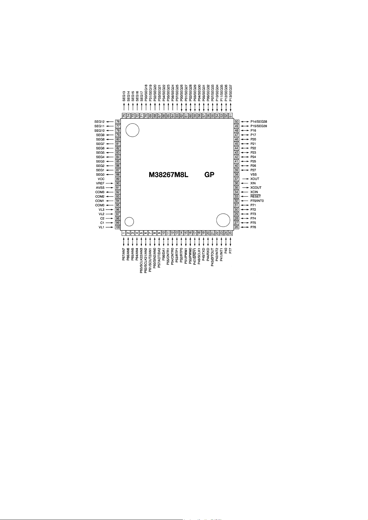
12) M3826M8L269GP (XA0818)
CPU
Terminal Connection
(TOP VIEW)
269
14
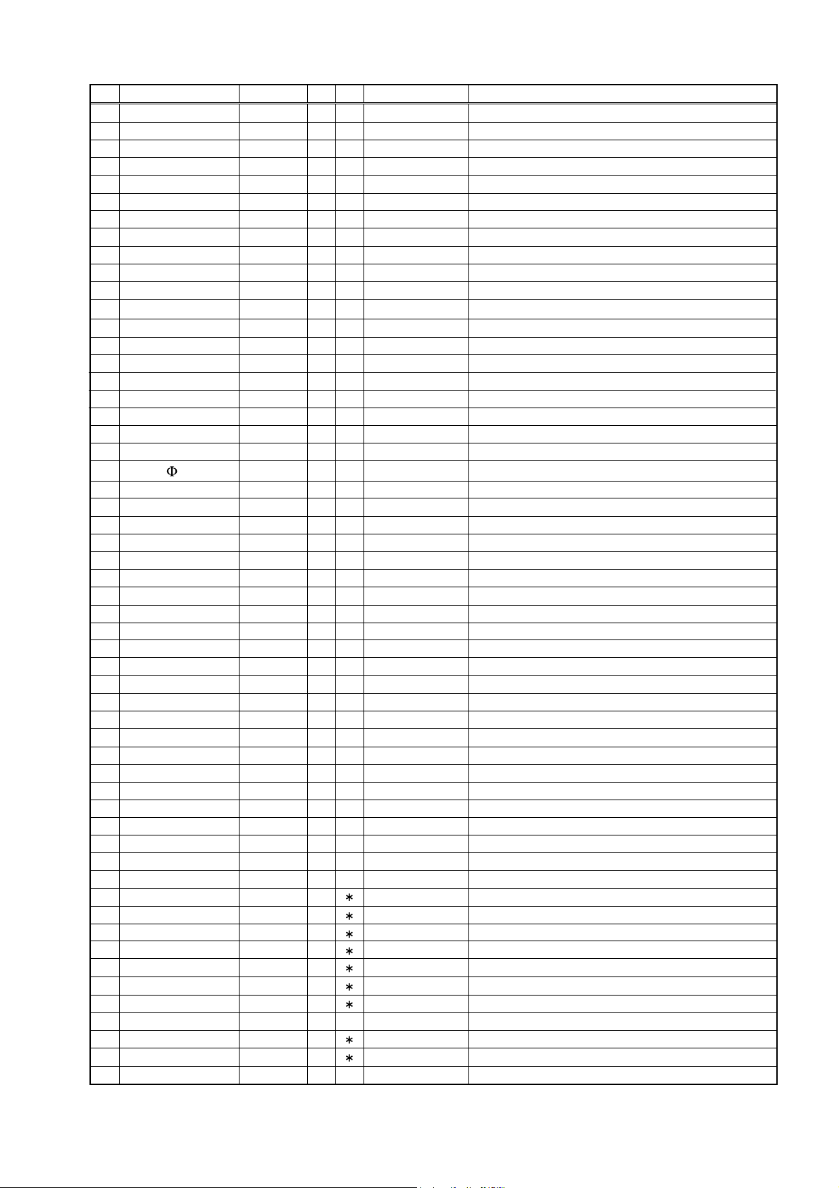
No. Pin Name Function I/O PU Logic Description
1 P67/AN7 SMT I - A/D S-meter input
2 P66/AN6 SQL I - A/D Noise level input for squelch
3 P65/AN5 BAT I - A/D Battery voltage input
4 P64/AN4 TIN I - A/D CTCSS tone input/DSC code input
5 P63/SCLK22/AN3 BP1 I - A/D Band plan 1
6 P62/SCLK21/AN2 BP2 I - A/D Band plan 2
7 P61/SOUT2/AN1 DCSW O - Activ high DCS signal mute
8 P60/SIN2/AN0 RE2 I - Activ low Rotary encoder input
9 P57/ADT/DA2 TOUT O - D/A CTCSS tone output/DCS tone output
10 P56/DA1 DOUT O - D/A DTMF output
11 P55/CNTR1 SCL O - Pulse Serial clock for EEPROM
12 P54/CNTR0 TBST O - Pulse Tone burst output
13 P53/RTP1 BP4 I - - Band plan 4
14 P52/RTP0 MUTE I/O - Activ low Microphone mute/Security alarm SW
15 P51/PWM3 CLK O - Pulse Serial clock output for PLL,scramble
16 P50/PWM DATA I/O - Pulse
17 P47/SRO Y1 TSTB I/O - Activ low/Pulse
Serial data output for PLL scramble/PLL unlock signal input
Trunking board detection / Strobe signal to trunking board
18 P46/SCLK1 STB O - Pulse Strobe for PLL IC
19 P45/TXD UTX O - Pulse UART data transmission output
20 P44/RXD RTX I - Pulse UART data reception output
21 P43/
/TOUT BEEP I/O - Pulse/Activ low Beep tone/Band plan 3
22 P42I/NT2 SEC I - Activ high Security voltage input
23 P41/INT1 RE1 I - Activ low Rotary encoder input
24 P40 DSQ I - Activ high Digital squelch input
25 P77 PTT I - Activ low PTT input
26 P7 SSTB O - Pulse/Activ low Strobe signal to scramble IC/Security mode
27 P75 W/N O - Activ low Wide Narrow SW
28 P74 T5 O - Activ low TX power ON/OFF output
29 P73 R5 O - Activ high RX power ON/OFF output
30 P72 SQC O - Activ low SQL ON/OFF
31 P71 C/S O - Activ low Digital scramble ON/OFF
32 P70/INTO BU I - Activ low Backup signal detection input
33 RESET RESET I - Activ low Reset input
34 Xcin Xcin - - - 35 Xcout Xcout - - - 36 Xin Xin - - - Main clock input
37 Xout Xout - - - Main clock output
38 Vss GND - - - CPU GND
39 P27 PSW I - Avtiv low Power switch input
40 P26 SDA O - Pulse Serial data for EEPROM
41 P25 C5C O - Activ high C5V power ON/OFF output
42 P24 AIR O - Activ high Air band SW / Tx middle power
43 P23 LOW O - Activ high Tx low power
44 P22 EXP O - Activ high T runking data SW
45 P21 SW6 I Activ low Key sw6 (SQL)
46 P20 SW5 I Activ low Key sw5 (CALL)
47 P17 SW4 I Activ low Key sw4 (TSQ)
48 P16 SW3 I Activ low Key sw3 (MHz)
49 P15/SEG39 SW2 I Activ low Key sw2 (V/M)
50 P14/SEG38 SW1 I Activ low Key sw1 (FUNC)
51 P13/SEG37 DOWN I Activ low Mic down input
52 P12/SEG36 DUD I - - Digital unit detect
53 P11/SEG35 SCR I Active low Scramble IC ready signal/Packet PTT
54 P10/SEG34 UP I Active low Mic down input
55 P07/SEG33 S33 O - - LCD segment signal
15
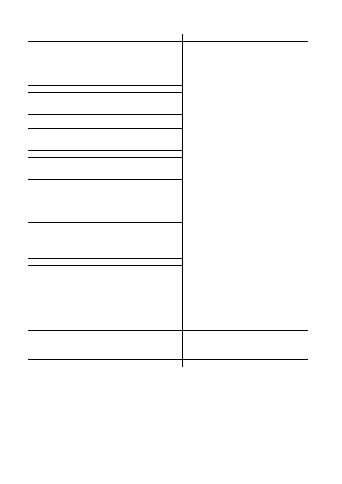
No. Pin Name Function I / O PU Logic Description
56 P06/SEG32 S32 O - 57 P05/SEG31 S31 O - 58 P04/SEG30 S30 O - 59 P03/SEG29 S29 O - 60 P02/SEG28 S28 O - 61 P01/SEG27 S27 O - 62 P00/SEG26 S26 O - 63 P37/SEG25 S25 O - 64 P36/SEG24 S24 O - 65 P35/SEG23 S23 O - 66 P34/SEG22 S22 O - 67 P33/SEG21 S21 O - 68 P32/SEG20 S20 O - 69 P31/SEG19 S19 O - 70 P30/SEG18 S18 O - 71 SEG17 S17 O - 72 SEG16 S16 O - 73 SEG15 S15 O - -
LCD segment signal
74 SEG14 S14 O - 75 SEG13 S13 O - 76 SEG12 S12 O - 77 SEG11 S11 O - 78 SEG10 S10 O - 79 SEG9 S9 O - 80 SEG8 S8 O - 81 SEG7 S7 O - 82 SEG6 S6 O - 83 SEG5 S5 O - 84 SEG4 S4 O - 85 SEG3 S3 O - 86 SEG2 S2 O - 87 SEG1 S1 O - 88 SEG0 S0 O - 89 Vcc VDD - - - CPU power terminal
90 Vref Vref - - - AD converter power supply
91 Avss Avss - - - AD converter GND
92 COM3 COM3 O - - LCD COM3 output
93 COM2 COM2 O - - LCD COM2 output
94 COM1 COM1 O - - LCD COM1 output
95 COM0 COM0 O - - LCD COM0 output
96 VL3 VL3 - - 97 VL2 VL2 - - -
LCD power supply
98 C2 I - - - 99 C1 C1 - - - -
100 VL1 VL1 I - A/D LCD power supply
16
SEMICONDUCT OR DATA
Downloaded by
RadioAmateur.EU
1) M5218FP (XA0068)
Dual Low Noise
Operational Amplifiers
Output 1
Inverting Input 1
Non Inverting Input 1
Power supply Minus
1
2
3
4
2) NJM7808FA (XA0102)
Pin Assignment
1. OUTPUT
2. COMMON
3. INPUT
Power Supply Plus
8
Output 2
7
Inverting Input 2
6
Non Inverting Input 2
5
123
3) TC4S66F (XA0115)
Bilateral Switch
17
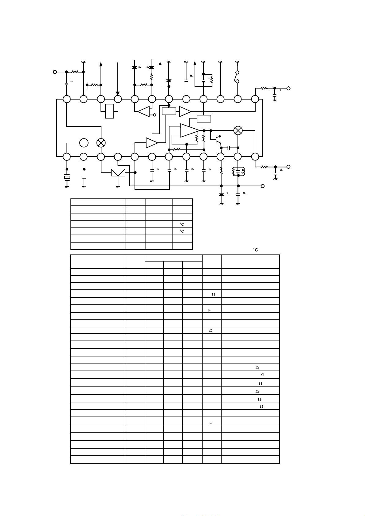
4) TK10930VTL (XA0223)
Narrow Band FM IF IC
IF IN
10.7MHz
51
Vcc
0.01
RF INPUT
24 23 22 21 20 19 18 17 16 15 14 13
30K 270K
GND
COMP OUT
COMP IN
NOISE AMP OUTPUT
F
1 F
1
+
+
1K
AM AGC
+
NOISE AMP INPUT
AM LOW CUT
0.033
RSSI OUT
0.1
68K
IF GND
AM SW
4.7K
AM AF OUT
AF OUTPUT (AM)
0.022
SQ
OSC
MIX
123456789101112
33p
OSC(E)
120p
10.245MHz OSC(B)
Vcc
MIX OUT
CFU455D
AMP
AM IF INPUT
+-
AM DET
AGC
F
0.1
DECOUPLING
IF AMP
F
0.1
FM IF INPUT
S DET
F
0.1
DECOUPLING
DECOUPLING
F
0.1
2.2K
+
FM DET
30K
LIM OUT
10 F
QUAD IN
7BRE-7437Z
0.1 F
FM AF OUT
Vcc 3V
Parameter Symbol Ratings Unit
Supply voltage Vcc max 10.0 V
Power dissipation Pd 400 mV
Storage temperature Tstg -55~+150
Operating temperature Top -30~+75
Operating voltage Vop 2.5~8.5 V
Operating frequency fop ~60 MHz
Parameter Symbol
Ratings
Min Typical Max
Unit Condition
Ta=25 Vcc=3V
Supply Current 1 lcc1 6.8 8.9 mA No signal, AM ON
Supply Current 2 lcc2 3.9 5.3 mA No signal, AM OFF
Mixer Coversion Gain Mg 20 dB
Mixer Input Impedance Mz 3.6 K
DC Test
FM
Limiting Sensitivity Limit 2.0 8.0
V -3.0dB
Output Voltage Vo1 85 150 230 mVrms 10mVin +/-3kHz DEV
Distortion THD1 1.0 2.0 % 10mVin +/-3kHz DEV
Output Impedance Zo 800
10mVin
Filter Gain Gf 30 38 dB Fin=30kHz, Vo=100mV
Scan Control Hi Voltage SH 2.3 V Squelch input=2.5V
Scan Control Low Voltage SL 0.3 V Squelch input=0V
Squelch Hysteresis Hys 30 mV
S meter Output Voltage S0 0.05 0.5 V Vin=0mV, RS=68k
S meter Output Voltage S1 0.05 0.5 0.9 V Vin=0.01mV, RS=68k
S meter Output Voltage S2 0.7 1.2 1.7 V Vin=0.1mV, RS=68k
S meter Output Voltage S3 1.2 1.8 2.5 V Vin=1mV, RS=68k
S meter Output Voltage S4 1.6 2.3 2.9 V Vin=10mV, RS=68k
S meter Output Voltage S5 1.8 2.4 2.9 V Vin=100mV, RS=68k
AM
Sensitivity US 20 15
required input level to get
V
20mV rms output
Output Voltage Vo2 60 120 160 mVrms 1kHz, 30%, Vin=1mV
Distortion-1 THD2 1.0 2.0 % 1kHz, 30%, Vin=1mV
Distortion-2 THD3 2.0 4.0 % 1kHz, 30%, Vin=1mV
S/N S/N 40 48 dB 1kHz, 30%, Vin=1mV
AM OFF Vo -0.3 0.3 %
AF OUTPUT (FM)
8.2K
0.01
18
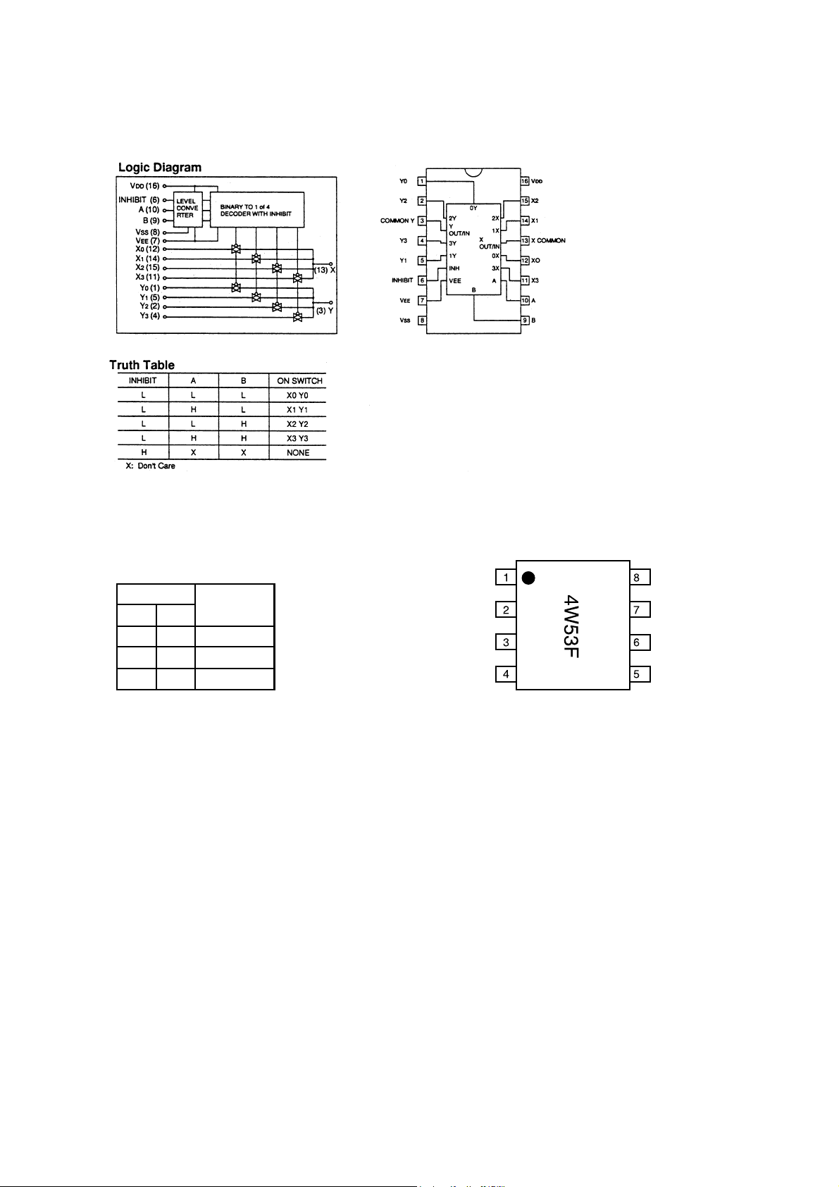
5) BU4052BF (XA0236)
Analog Multiplexer/Demultiplexer
6) TC4W53FU (XA0348)
Multiplexer/Demultiplexer
Function T able
Control input
INH
L
L
H
* Don't Care
A
L
H
*
ON channel
ch0
ch1
NONE
COMMON
INH
VEE
VSS
VDD
ch0
ch1
A
19
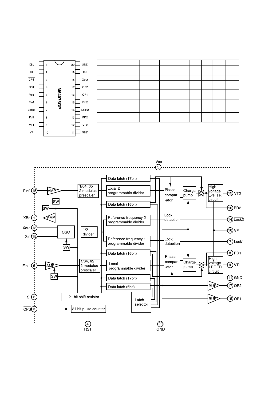
7) M64076GP (XA0352)
Dual PLL Synthesizer
Equivalent Circuit
Parameter Symbol Condition Min. Typ. Max. Unit
Power supply voltage Vcc
LPF supply voltage VF
Local oscillator input level Vin
Local oscillator input frequency Fin
Xin input level Vxin
Xin input frequency Fxin
Fin=80~520MHz
Vin=-10dBm
Fin=80~520MHz
Vin=-20~-4dBm
Vcc=2.7~5.5V
Vcc=2.7~5.5V
Vcc=2.7~5.5V
Fxin=10~25MHz
Sine wave
Vcc=2.7~5.5V
Vxin=0.4~1.4Vp-p
2.7 - 5.5 V
-912V
-20 - -4 dBm
80 - 520 MHz
0.4 - 1.4 Vp-p
10 - 25 MHz
20
8) LA4425A (XA0410)
5W Audio Power Amplifiers
Test Circuit
Vcc
13.2V
+
LA4425
Input
1
+
2
F
2.2
Vcc=13.2V RL=4 Po =5W Gain= 45dB
9) M67746 (XA0412)
144 ~ 148MHz 60W
RF Power Module
Fin(Ground)
4
+
1000
1000 F
F
SP
4
12345
Rating Symbol Ratings Unit
Supply voltage Vcc 17 V
Total current Icc 20 A
Fin(Ground)
Input power Pin(max) 600 mW
Output Power Po(max) 70 W
Operation case temperature Tc(op) -30 to + 110
Strage temperature Tstg -40 to + 110
Zg=Zl=50
5
3
Input terminal
(300mW)
1st stage DC
supply
terminal(12.5V)
Final DC supply
terminal (12.5V)
Output
terminal (60W)
21
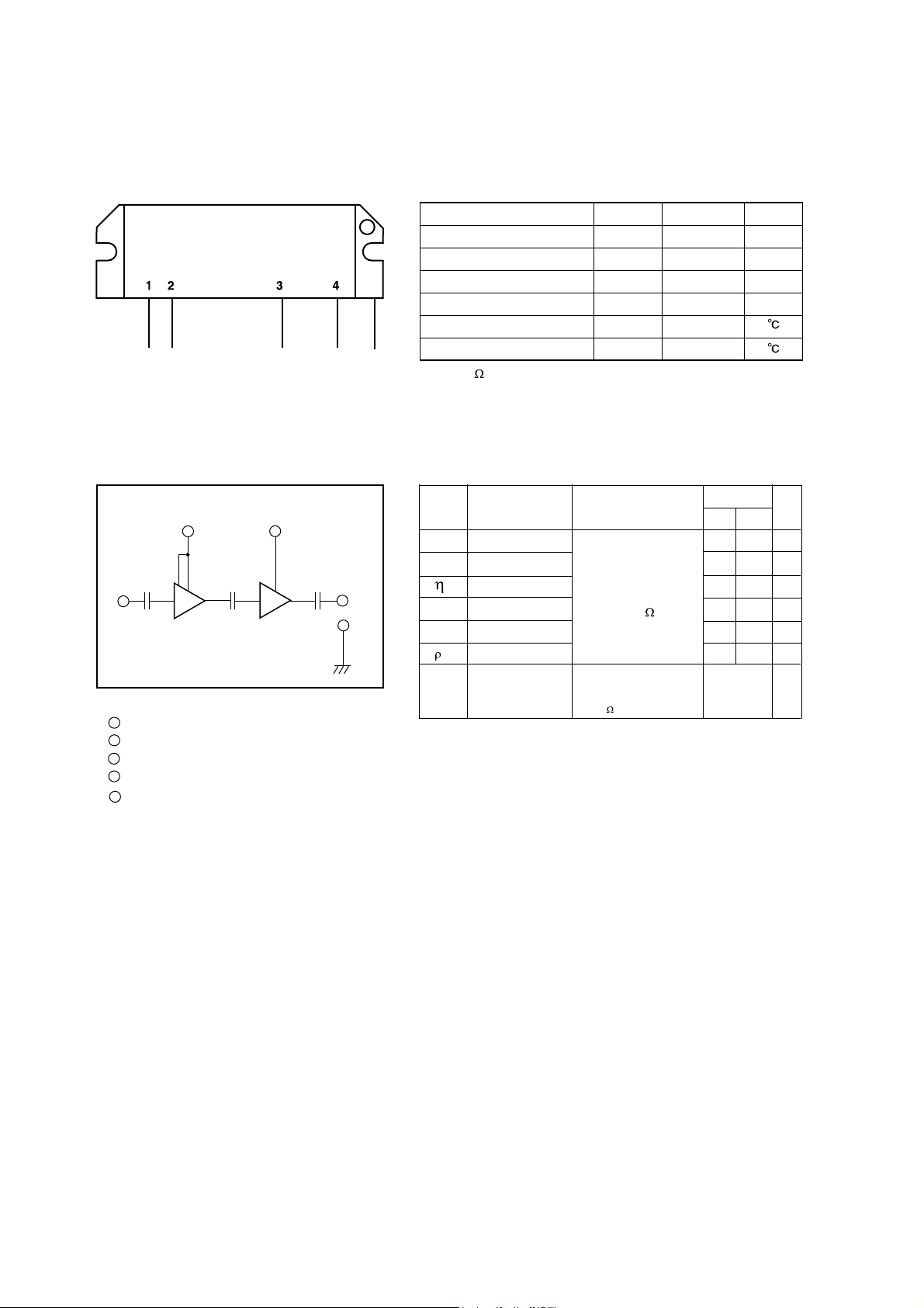
10) M68729 (XA0591)
220 ~ 246MHz 30W
RF Power Module
M68729
Fin(Ground)
5
ABSOLUTE MAXIMUM RATING(TC = 25˚C)
Rating Symbol Ratings Unit
Supply voltage Vcc 17 V
Total current Icc 10 A
Fin(Ground)
Input power Pin(max) 600 mW
Output Power Po(max) 40 W
Operation case temperature Tc(op) -30 to + 110
Strage temperature Tstg -40 to + 110
Zg=Zl=50
Input terminal
(300mW)
1st stage DC
supply
terminal(12.5V)
Block Diagram
2
1
PIN :
1
Pin : RF INPUT
2
CC1
V
3
V
4
PO : RF OUTPUT
5
GND : FIN
: 1st. DC SUPPLY
CC2
: 2nd. DC SUPPLY
Final DC supply
terminal (12.5V)
Output
3
GND (FIN)
terminal (60W)
4
5
ELECTRICAL CHARACTERISTICS
Symbol
f
Po
T
2fo
3fo
in
Parameter
Frequency range
Output power
Total efficiency
2nd. harmonic
3rd. harmonic
Input VSWR
Load VSWR tolerance
Test conditions
V
CC1,2
= 12.5V
Pin = 300mV
G
= ZL = 50
Z
V
CC1,2
= 15.2V
Po = 30W(Pin = Controlled)
Load VSWR = 20:1 (All phase),
G
= 50
Z
Limits
Min
Max
Unit
220 246 MHz
-30
-30
W
%
dBc
dBc
30
40
3
No degradation
or destroy
-
--
22
 Loading...