


®
INSTALLATION & SERVICE
MANUAL
SINGLE CHANNEL
POWER AMPLIFIER
NTGS86AA
869-894 MHz
25 WATTS AVERAGE POWER
12 August 1998
Powerwave Technologies, Inc. Tel: 949-757-0530
2026 McGaw Avenue Fax: 949-757-0941
Irvine, CA 92614 Web Site: www.pwav.com
TABLE OF CONTENTS
044-05045 Rev. A

Par. Section 1 Page
No. General Description No.
1-1 Introduction ............................................................................................ 1-1
1-2 General Description .............................................................................. 1-1
1-3 Functional and Physical Specifications .................................................. 1-1
Section 2
Installation
2-1 Introduction ............................................................................................ 2-1
2-2 Electrical Service Recommendations..................................................... 2-1
2-3 Unpacking and Inspection...................................................................... 2-1
2-4 Installation Instructions........................................................................... 2-2
2-5 Amplifier Module Power, Alarm, and Control Connector........................ 2-2
2-6 RS485 Connector................................................................................... 2-3
Section 3
Operating Instructions
3-1 Introduction ............................................................................................ 3-1
3-2 Initial Start-Up and Operating Procedures ............................................. 3-1
Section 4
Principles of Operation
4-1 Introduction ............................................................................................ 4-1
4-2 RF Input Signal ...................................................................................... 4-1
4-3 RF Output Load...................................................................................... 4-1
4-4 Amplifier Functional Description............................................................. 4-1
4-4.1 Main Amplifier ........................................................................................ 4-2
4-4.2 Amplifier Monitoring ............................................................................... 4-3
4-4.3 Amplifier Module Cooling ....................................................................... 4-3
4-5 Power Distribution .................................................................................. 4-3
Section 5
Maintenance
5-1 Introduction ............................................................................................ 5-1
5-2 Periodic Maintenance............................................................................. 5-1
5-3 Test Equipment Required For Test ........................................................ 5-1
5-4 Performance Test................................................................................... 5-2
5-4.1 Amplifier Performance Test.................................................................... 5-2
5-5 Field Replacement of the Module .......................................................... 5-7
2

TABLE OF CONTENTS (Continued)
Par. Section 6 Page
No. Troubleshooting No.
6-1 Introduction .............................................................................................6-1
6-2 Troubleshooting ......................................................................................6-1
6-3 Return for Service Procedures................................................................6-1
6-3.1 Obtaining an RMA...................................................................................6-1
6-3.2 Repackaging for Shipment......................................................................6-1
LIST OF ILLUSTRATIONS
Figure Page
No. No.
1-1 NTGS86AA Single Channel Power Amplifier ......................................... 1-3
2-1 Power, Alarm, and Control Connector (18-Pin Molex) ........................... 2-2
2-2 RS485 Connector................................................................................... 2-3
4-1 NTGS86AA Single Channel Power Amplifier Functional Block Diagram 4-2
5-1 NTGS86AA Amplifier Test Setup Diagram ............................................ 5-3
5-2 RF Input (CDMA Source) ....................................................................... 5-3
LIST OF TABLES
Table Page
No. No.
1-1 NTGS86AA Single Channel Power Amplifier Functional Specifications.....
1-2
2-1 18-Pin Molex Alarm, Control, and Power Connections .......................... 2-3
2-2 RS485 Pin Definition.............................................................................. 2-3
5-1 Periodic Maintenance............................................................................. 5-1
5-2 Test Equipment Required ...................................................................... 5-2
5-3 Single Channel Power Amplifier Test Data Sheet.................................. 5-4
6-1 Troubleshooting ..................................................................................... 6-1
3

Section
1
GENERAL DESCRIPTION
1-1. INTRODUCTION
This manual contains information and procedures for installation, operation, and maintenance of
Powerwave’s model NTGS86AA single channel power amplifier (SCPA). The manual is organized
into six sections as follows:
Section 1. General Description
Section 2. Installation
Section 3. Operating Instructions
Section 4. Principles of Operation
Section 5. Maintenance
Section 6: Troubleshooting
1-2. GENERAL DESCRIPTION
The NTGS86AA is a linear, single-channel power amplifier that operates in the 25 MHz frequency
band from 869 MHz to 894 MHz. It is designed as a self-contained module with EMI containment
for use in both an indoor and outdoor North American Cellular Base Stations. Its flat base plate
allows for mounting on a flat thermal-absorbing surface to provide adequate heat dissipation,
thereby avoiding the use of any built-in fans.
Each amplifier module has a power, alarm, and control connector that allows the host system to
monitor the amplifier module performance. Primary power for the amplifier is +26 Vdc.
1-3. FUNCTIONAL AND PHYSICAL SPECIFICATIONS
Functional and physical specifications for the amplifier are listed in table 1-1.
4

Table 1-1. NTGS86AA Single Channel Power Amplifier Functional Specifications
Frequency Range 869-894 MHz (25 MHz Bandwidth)
Maximum Average Input Power 13 dBm
Continuous Average Output Power 25 Watts
Spurious Emissions @ Maximum
Rated Output Power (44 dBm)
RF Gain 43 ±2 dB
Gain Flatness:
Output Protection: Mismatch Protected
Input Port Return Loss: VSWR 2:1 Max.
Out of Band Spurious: Less than -14 dBm
DC Input Power:
Operating Temperature: -15 ºC. to +85 ºC. (heatsink temperature)
Storage Temperature: -40 ºC. to +70 ºC.
Operating Humidity: 5 % - 95 % Relative Humidity (Noncondensing)
Storage Humidity: 5 % - 95 % Relative Humidity (Noncondensing)
DC Input, Alarm, and Control
Connector:
RF Input Connector: SMA Female
RF Output Connector: SMA Female
RF Sample Connector:
Dimensions (inches): Width: 12.515; depth: 9.900; height: 1.670
Frequency Requirement Meas. Bandwidth
750 kHz offset -46 dBc 30 kHz
1.23 MHz offset -61 dBc 30 kHz
1.5 MHz offset -61 dBc 30 kHz
1.98 MHz offset -61 dBc 30 kHz
±
0.15 dB for any 2-MHz band within frequency range.
+26 ± 0.5 Vdc, 260 mV p-p max. ripple, ≤350 watts
18-Pin Molex
SMA Female (27±1 dB below RF Output)
5
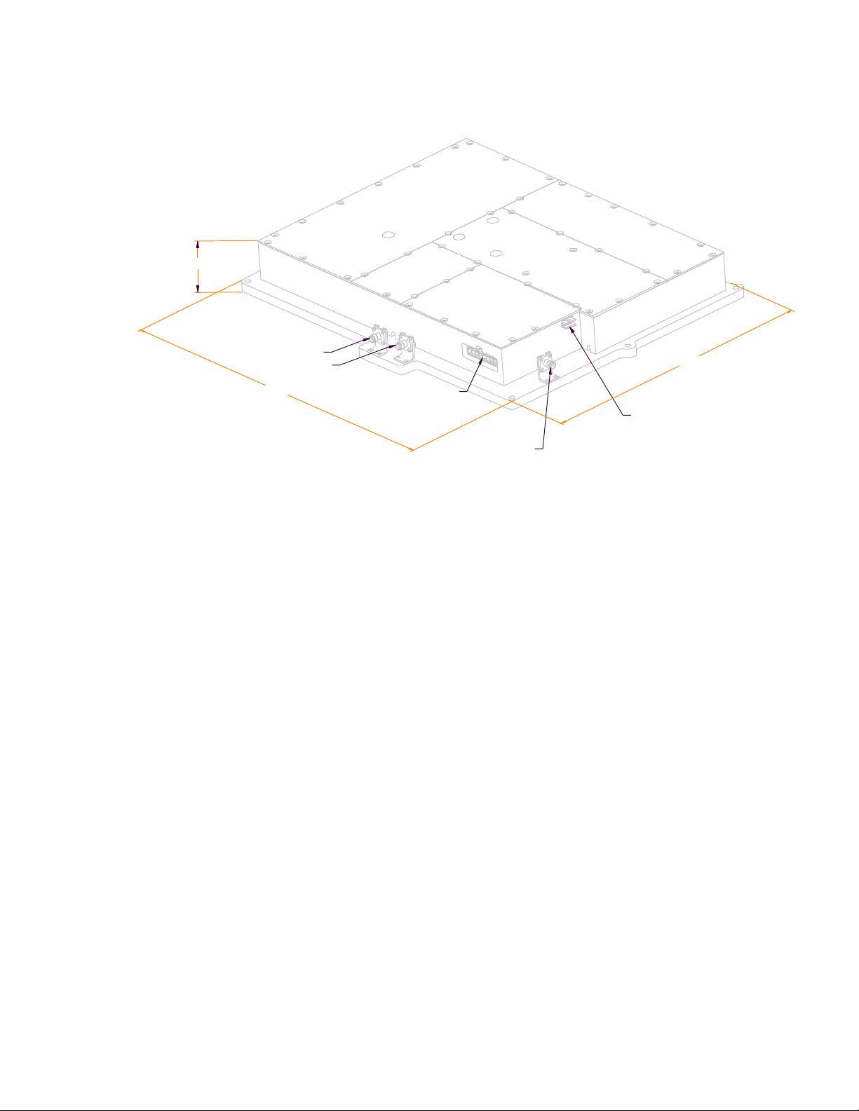
RF OUTPUT
RF INPUT
9.900
12.515
18 PIN MO LEX CONNE CTOR
RS485 CONNECTOR
Figure 1-1. NTGS86AA Single Channel Power Amplifier
6

Section
2
INSTALLATION
2-1. INTRODUCTION
This section contains unpacking, inspection, and installation instructions and recommendations for
the Model NTGS86AA Single Channel Power Amplifier. Carefully read all material in this section
prior to equipment unpacking or installation. Also read and review the operating procedures in
Section 3 prior to installing the equipment. It is important that the licensee perform these tasks
correctly and in good faith. If applicable, carefully read Parts 73 and 74 of the Federal
Communications Commission (FCC) rules to determine how they apply to your installation. DON'T
TAKE CHANCES WITH YOUR LICENSE.
2-2. ELECTRICAL SERVICE RECOMMENDATIONS
Powerwave Technologies recommends that proper AC line conditioning and surge suppression be
provided on the primary AC input to the +26 Vdc power source. All electrical service should be
installed in accordance with the National Electrical Code, any applicable state or local codes, and
good engineering practice. Special consideration should be given to lightning protection of all
systems in view of the vulnerability of most transmitter sites to lightning. Lightning arrestors are
recommended in the service entrance. Straight, short ground runs are recommended. The
electrical service must be well grounded.
Each amplifier system should have its own circuit breaker, so a failure in one does not shut off the
whole installation. Circuit breakers should be thermal type, capable of handling the maximum
anticipated inrush current, in a load center with a master switch.
2-3. UNPACKING AND INSPECTION
This equipment has been operated, tested and calibrated at the factory. Carefully open the
container(s) and remove the amplifier module(s). Retain all packing material that can be
reassembled in the event that the unit must be returned to the factory.
CAUTION
Exercise care in handling equipment
during inspection to prevent damage
caused by rough or careless handling.
Visually inspect the amplifier module for damage that may have occurred during shipment. Check
for evidence of water damage, bent or warped chassis, loose screws or nuts, or extraneous packing
material in the connector. If the equipment is damaged, a claim should be filed with the carrier
once the extent of any damage is assessed. We cannot stress too strongly the importance of
IMMEDIATE careful inspection of the equipment and the subsequent IMMEDIATE filing of the
necessary claims against the carrier if necessary. If possible, inspect the equipment in the
presence of the delivery person. If the equipment is damaged, the carrier is your first area of
recourse. If the equipment is damaged and must be returned to the factory, write or phone for a
return authorization. Powerwave may not accept returns without a return authorization. Claims for
loss or damage may not be withheld from any payment to Powerwave, nor may any payment due
be withheld pending the outcome thereof. WE CANNOT GUARANTEE THE FREIGHT
CARRIER'S PERFORMANCE
7

2-4. INSTALLATION INSTRUCTIONS
The NTGS86AA amplifier module is designed for installation on a heatsink that permits access to
the module for connection of RF cables and the power, alarm, and control connector.
To install the amplifier proceed as follows:
1. Install amplifier on heatsink with thermally conductive material inserted between amplifier
module and heatsink, and secure in place with four mounting screws.
2. Connect the antenna cable to
3. Connect the transceiver output cable to
(Refer to figure 1-1)
RF OUT
SMA connector.
RF IN
SMA connector.
4. Connect coupled RF output monitor cable to
Turn off external primary DC power before
connecting cable to 18-pin Molex connector.
5. Connect power, alarm, and control cable to 18-pin Molex connector.
6. Check your work before applying DC voltage to the system. Make certain all connections are
tight and correct.
7. Measure primary DC input voltage. DC input voltage should be +26 ±0.5 Vdc. If the DC input
voltage is above or below the limits, call and consult Powerwave before you turn on your
amplifier system.
8. Refer to section 3 for initial turn-on and checkout procedures.
2-5. AMPLIFIER MODULE POWER, ALARM, AND CONTROL CONNECTOR
The power, alarm, and control connections on the amplifier are made through an 18-pin Molex
connector (figure 2-1) and are listed and described in table 2-1.
RF SAMPLE
WARNING
SMA connector.
Figure 2-1. Power, Alarm, and Control Connector (18-Pin Molex)
8

TTaabbllee 22--11.. 1188--PPiinn MMoolleexx AAllaarrmm,, CCoonnttrrooll,, aanndd PPoowweerr CCoonnnneeccttiioonns
PIN SIGNAL DESCRIPTION SIGNAL NAME
1 Temperature Output (0-4.7 volts) TEMP_OUT
2 Reverse Power Detection (0-4.7 volts) REV_PWR
3 Forward Power Detection (0-4.7 volts) FWR_PWR
4 Ground GND
5NCNA
6
7 Ground GND
8 Ground GND
9 Ground GND
10 + Anxiety output (RS 422 level) ANX (+)
11 + Enable input (RS 422 level) ENABLE (+)
12
13 + Alarm output (RS 422 level) ALARM (+)
14
15 +26 Vdc VDD
16 +26 Vdc VDD
17 +26 Vdc VDD
18 +26 Vdc VDD
2-6. RS485 CONNECTOR
The RS485 connector (figure 2-2) allows the user to monitor the status of the amplifier, download
new firmware, and revise the amplifier attributes. The pin connections are defined in table 2-2.
−
Anxiety output (RS 422 level)
−
Enable input (RS 422 level) ENABLE (−)
−
Alarm output (RS 422 level) ALARM (−)
ANX (-)
s
1
Figure 2-2. RS485 Connector
Table 2-2. RS485 Pin Definition
PIN
1Rxd+
2
3
4Txd+
FUNCTIO
N
−
Rxd
−
Txd
4
9

Section
3
OPERATING INSTRUCTIONS
3-1. INTRODUCTION
This section contains operating instructions for the Multicarrier Cellular Amplifier.
3-2. INITIAL START-UP AND OPERATING PROCEDURES
There are no operating controls or indicators on the NTGS86AA amplifier module. To perform the
initial start-up, proceed as follows:
1. Double check to ensure that all input and output cables are properly connected.
CAUTION
Before applying power, make sure that the input and output of the
amplifier are properly terminated at 50 ohms. Do not operate the
amplifier without a load attached. Refer to table 1-1 for input power
requirements. Excessive input power may damage the amplifier
NOTE
The output coaxial cable between the amplifier and the antenna must
be 50 ohm coaxial cable. Use of any other cable will distort the output.
2. Turn on supply that provides +26 Vdc to the amplifier system.
3. Turn on external exciter/transceiver and apply RF input signals.
Section
4
PRINCIPLES OF OPERATION
4-1. INTRODUCTION
This section contains a functional description of the Single Channel Power
Amplifier (SCPA).
4-2. RF INPUT SIGNAL
The maximum input power should not exceed the limits specified in table 1-1.
10

4-3. RF OUTPUT LOAD
The load impedance should be as good as possible (1.5:1 or better) in the working
band for good power transfer to the load.
4-4. AMPLIFIER FUNCTIONAL DESCRIPTION
The NTGS86AA amplifier (figures 1-1 and 4-1) is a linear, single-channel power
amplifier that operates in the 25 MHz frequency band from 869 MHz to 894 MHz
at an output power of 25 watts. Each amplifier is a self-contained module and is
functionally independent of any other amplifier modules in the system. Each
amplifier module has an alarm board that monitors the amplifier performance. If a
failure or fault occurs in an amplifier module, it is transmitted to the host system
via an 18-pin Molex connector.
The amplifier is compliant to the requirements of FCC Part 22 and TIA/EIA IS97A
with respect to spurious emissions (see table 1-1). Constant gain is maintained by
continuously comparing active paths with passive references, and correcting for
small variations through the RF feedback controls. All gain variations, for example
those due to temperature, are reduced to the passive reference variations. The
amplifier module is comprised of:
A three-stage driver amplifier
A main amplifier
Alarm monitoring and control
A spurious emission detection DSP circuit
4-4.1. THREE-STAGE DRIVER AMPLIFIER
The input of the amplifier employs three stages of class AB amplification which
provide approximately 33 dB of gain in the 25 MHz frequency band from 869 MHz
to 894 MHz. The amplifier operates on +26 Vdc, and a bias voltage of +5 Vdc,
and is mounted directly on a heat sink. The alarm logic controls the +5 Vdc bias
voltage that shuts down the amplifier.
4-4.2. MAIN AMPLIFIER
The main amplifier employs class AB amplification for maximum efficiency. The
signal provides approximately 10 dB of gain in the 25 MHz frequency band. The
output from the main amplifier is typically 30 watts. The amplifier operates on +26
Vdc, and a bias voltage of +5 Vdc, and is mounted directly on a heat sink. The
alarm logic controls the +5 Vdc bias voltage that shuts down the amplifier.
11

Three Stage
Driver
Main Amp
RF
IN
33dB
Gain
Phase,
Gain,
and
Bias
Control
10dB
Gain
Phase,
Gain,
and
Bias
Control
SPURIOUS DETECTION
DSP CIRCUIT
ALARM CIRCUIT
Figure 4-1. NTGS86AA Single Channel Power Amplifier Functional Block
Diagram
RF
OUT
Optimize
the
spurious
emissions
mask
of the
CDMA
output
signal
4-4.3. ALARM MONITORING AND CONTROL
In the amplifier, all normal variations are automatically compensated for by the
spurious detector control. However, when large variations occur beyond the
adjustment range of the loop control, a loop fault will occur. The alarms are output
via an 18-pin Molex connector on the module for subsequent remote monitoring.
4-4.4. SPURIOUS EMISSION DETECTION DSP CIRCUIT
The primary function of the spurious detection circuit is to monitor the spurious
emissions mask of the RF signal at all amplifier stages. DSP circuitry is used to
control the phase, gain, and bias of all amplifier stages, thereby optimizing the
spurious emissions mask of the CDMA output signal.
4-5. AMPLIFIER MODULE COOLING
Each amplifier module is contained within a thermally conductive chassis which,
when properly mounted on an adequate thermal surface, will provide sufficient
cooling to maintain the amplifier within the specified operating temperature range.
4-6. POWER DISTRIBUTION
Primary DC power for the amplifier is provided by the host system. The amplifier
module has a DC/DC converter that converts the +26 Vdc to +15 Vdc, +5 Vdc and
+8 Vdc.
12

Section
5
MAINTENANCE
5-1. INTRODUCTION
This section contains periodic maintenance and performance test procedures for the Single
Channel Power Amplifier. It also contains a list of test equipment required to perform the identified
tasks.
NOTE
Check your sales order and equipment
warranty before attempting to service or
repair the unit. Do not break the seals on
equipment under warranty or the warranty
will be null and void. Do not return
equipment for warranty or repair service
until proper shipping instructions are
received from the factory.
5-2. PERIODIC MAINTENANCE
Periodic maintenance requirements are listed in Table 5-1. Table 5-1 also lists the intervals at
which the tasks should be performed.
Table 5-1. Periodic Maintenance
TASK INTERVAL ACTION
Inspection
Cables and
Connectors
Performance Tests
5-3. TEST EQUIPMENT REQUIRED FOR TEST
Test equipment required to test the amplifier is listed in Table 5-2. Equivalent test equipment may
be substituted for any item, keeping in mind that a thermistor type power meter is required.
All RF test equipment must be calibrated to 0.05
dB resolution. Any deviation from the nominal
attenuation must be accounted for and factored
into all output readings.
12 Months
12 Months
NOTE
IInnssppeecctt ssiiggnnaall aanndd ppoowweerr ccaabbllees
ffoorr ffrraayyeedd iinnssuullaattiioonn.. CChheecckk RRF
ccoonnnneeccttoorrss ttoo bbee ssuurree tthhaatt tthheey
aarree ttiigghhtt.
PPeerrffoorrmm aannnnuuaall tteesstt ppeer
ppaarraaggrraapphh 55--55.
.
r
.
F
y
s
13

Table 5-2. Test Equipment Required
MANUFACTURER MODEL
MENCLATURE
Signal Generator H.P. 8656B
20 dB Attenuator, 250 Watt Tenuline
20 dB Attenuator, 20 Watt (2 each) Tenuline
Spectrum Analyzer H.P. 8560E
Coax Directional Coupler H.P. 778D
Power Meter / Sensor H.P. 437B / 8481A
Arbitrary Waveform Generator Sony AWG2021
Network Analyzer H.P. 8753C
Current Probe
Source Diskette Powerwave
CDMA Generator Noise Com 800-1
5-4. PERFORMANCE TEST
Performance testing should be conducted every 12 months to ensure that the amplifier system
meets the operational specifications listed in table 5-3. Also verify system performance after any
amplifier module is replaced in the field. The test equipment required to perform the testing is listed
in table 5-2, and the test setup is shown in figure 5-1.
NOTE
The frequencies used in this test are typical for an amplifier with a
25 MHz band from 869 MHz to 894 MHz. Select evenly spaced
F1, F2, F3, and F4 frequencies that cover the instantaneous
bandwidth of your system.
5-4.1. AMPLIFIER PERFORMANCE TEST.
To perform the test, proceed as follows:
1. Connect test equipment as shown in figure 5-1.
NOTE
Do not apply any RF signals at this time.
AMPLIFIER SPURIOUS EMISSIONS TEST:
2. With the RF input signal to the amplifier set to be as shown in figure 5-2, use the spectrum
analyzer to measure the spurious emissions performance. Record test data in table 5-3.
Verify that it is within the specifications shown in table 1-1. Switch tested amplifier to OFF.
GAIN TEST:
3. Disconnect spectrum analyzer from test setup, and connect the network analyzer.
4. Set network analyzer as follows:
a. Power output to 11 dBm.
b. Frequency start to 869 MHz.
c. Frequency stop to 894 MHz.
d. Normalize the network analyzer for gain and return loss.
5. Check the amplifier gain across the band from 869 MHz to 894 MHz. Gain should be as
specified in table 1-1 ±1 dB. Record test data in table 5-3.
14

INPUT RETURN LOSS TEST:
6. Read and record the S
table 5-3.
return loss measurement on network analyzer. Record test data in
11
Figure 5-1. NTGS86AA Amplifier Test Setup Diagram
15

Table 5-3. Single Channel Power Amplifier Test Data Sheet
DATE__________________________________
MODULE S/N ___________________________
TEST CONDITIONS:
Load and Source Impedance: 50 Ohms
VSWR: < 1.2:1
Supply Voltage: +26 Vdc ±0.1 Vdc
TEST SPECIFICATION MIN MAX
DATA
RF Gain Vcc = 26 Vdc
PO = 25 W
Freq. = 880 MHz
Spurious
Emissions
Gain Flatness Vcc = 26 Vdc
Input Return
Loss
PASS FAIL
Tested by
Vcc = 26 Vdc
PO =25 W
869 - 894 MHz Band
PO =25 W
869 - 894 MHz Band
Vcc = 26 Vdc
PO = 25 W
869-894 MHz Band
Table 1-1
-1 dB
-18 dB
Table 1-1
+1 dB
-65 dBc
±0.7 dB
16

5-5. FIELD REPLACEMENT OF THE MODULE
The NTGS86AA single channel power amplifier module can be replaced in the field on site by a
qualified technician with experience maintaining RF power amplifiers and similar equipment:
To replace a power amplifier module, proceed as follows:
1. Turn off 26 Vdc power to that specific module.
2. Disconnect the three RF cables, 18-pin Molex cable, and RS485 cable.
3. Loosen four screws that secure amplifier module to heat sink.
4. Carefully remove amplifier module from heat sink.
5. Install replacement in reverse order of steps 1 through 4 above.
Section
6
TROUBLESHOOTING
6-1 INTRODUCTION
This section contains a list of problems which users have encountered and a few suggested actions
that may correct the problem. If the suggested corrective action does not eliminate the problem,
please contact your Powerwave field representative or the factory for further instructions.
NOTE
Check your sales order and equipment
warranty before attempting to service or
repair the unit. Do not break the seals on
equipment under warranty or the warranty
will be null and void. Do not return
equipment for warranty or repair service
until proper shipping instructions are
received from the factory.
6-2 TROUBLESHOOTING
Refer to table 6-1 for troubleshooting suggestions.
Table 6-1. Troubleshooting.
SYMPTOM SUGGESTED ACTION
SCPA Inoperative 1. Check for proper power supply voltage.
SCPA Not Enabled 1. Verify RS 422 + (ENABLE signal) is high.
11.. VVeerriiffyy DDCC ssuuppppllyy iiss ≤≤2288..55±±00..2255 VVddc
Anxiety Output is RS 422
High
2. Verify TEMP_OUT <5 °C above maximum sensor temp.
3. Verify RF input <6 dBm ±0.5 dB; remove overdrive and
toggle ENABLE input.
c
17

Alarm Output is RS 422 High Verify input RF is within specified power and frequency limits
6-3 RETURN FOR SERVICE PROCEDURES
When returning products to Powerwave, the following procedures will ensure optimum response.
6-3.1 Obtaining an RMA
A Return Material Authorization (RMA) number must be obtained prior to returning
equipment to the factory for service. Please contact our Customer Service Department at
(949) 757-0530 to obtain this number. Failure to obtain this RMA number will result in
considerable delays in receiving repair service.
6-3.2 Repackaging for Shipment
To ensure safe shipment of the amplifier, it is recommended that the package designed for
the amplifier be used. The original packaging material is reusable. If it is not available,
contact Powerwave’s Customer Service Department for packing materials and information.
18
 Loading...