


R&D –SERVICE MANUAL DT0489-E00
Powertronix spa reserves the right to modify this document without notice
POWERTRONIX
Mizar-Alcor
Service Manual
Document : DT0489 English PTX
Revision
Date Checked Approved
00
07-09-2009 07-09-2009
Ghezzi R.
07-09-2009
Ghezzi R.

R&D –SERVICE MANUAL DT0488
Powertronix spa reserves the right to modify this document without notice
Page. 2 of 72
Index
1. GENERAL ITEMS......................................................................................................4
1.1 INTRODUCTION...................................................................................................4
1.1.1 GENERAL FAULT IDENTIFICATION PROCEDURE...................................4
1.2 TOOLS..................................................................................................................5
1.2.1 PORTABLE PC WITH SOFTWARE.............................................................5
1.2.2 OSCILLOSCOPE .........................................................................................5
1.2.3 DIGITAL MULTIMETER (DSM)....................................................................5
1.2.4 DISCHARGING RESISTOR.........................................................................5
2 UPS COMPONENTS RECOGNIZING .......................................................................6
2.1 UPS CLOSED.......................................................................................................6
2.2 INNER VIEW WITH SAFETY COVER REMOVED...............................................7
2.3 REAR UPS DESCRIPTION..................................................................................8
2.4 UPS-10-15KVA ELECTRONIC PARTS LAYOUT.................................................9
2.5 UPS-20-30KVA ELECTRONIC PARTS LAYOUT...............................................10
2.6 UPS-10-15KVA BOARDS..................................................................................11
2.7 UPS-20-30KVA BOARDS..................................................................................11
2.8 BOARDS LAYOUT..............................................................................................12
2.8.1 UPS-10-15KVA POWER INTERFACE BOARD COMPONENT LAYOUT..12
2.8.2 UPS-20-30KVA POWER INTERFACE BOARD COMPONENT LAYOUT..13
2.8.3 CS0150 UPS-10-15KVA UPS-20-30KVA CONTROL BOARD...................14
2.8.4 CS0153 UPS-10-15KVA UPS-20-30KVA POWER SUPPLY BOARD........15
2.8.5 CS0098 RELAY & COMUNICATION BOARD............................................16
2.8.6 SNMP COMUNICATION BOARD...............................................................16
2.8.7 TERMINAL BLOCKS..................................................................................17
3 TROUBLESHOOTING.............................................................................................18
3.1 POWER FUSE....................................................................................................18
3.1.1 UPS-10-15KVA...........................................................................................18
3.1.2 UPS-20-30KVA...........................................................................................19
3.2 CHECK ALL PFC & INVERTER OUT IGBTS.....................................................20
3.2.1 UPS-10-15KVA...........................................................................................20
3.2.2 UPS-20-30KVA...........................................................................................21
3.2.3 CHECK AUXILIARY POWER SUPPLY CONTROL BOARD......................23
3.2.4 LED STATUS .............................................................................................25
3.2.5 CHECK CONTROL BOARD.......................................................................26
3.2.6 CHECK POWER SUPPLY VOLTAGE........................................................26
3.3 POWER INTERFACE UPS-10-15KVA BOARD..................................................27
3.4 POWER INTERFACE UPS-20-30KVA BOARDS (CS0151)...............................29
4 PC BASED CHECKS AND SETTINGS ...................................................................31
5 ELECTRICAL DIAGRAM.........................................................................................40
5.1 PCB ELECTRICAL DIAGRAM INDEX................................................................40
5.1.1 DE1237 UPS 10-15KVA GENERAL DIAGRAM .........................................41
5.1.2 DE1112 UPS 20-30KVA GENERAL DIAGRAM .........................................43
5.1.3 DE0098 RELAY & COMMUNICATION BOARD.........................................46
5.1.4 DE0138 TEMPERATURE SENSOR PCB..................................................47

R&D –SERVICE MANUAL DT0488
Powertronix spa reserves the right to modify this document without notice
Page. 3 of 72
5.1.5 DE0143 BATTERY FUSE PCB (BATTERY 7.2-9AH) / DE0157 BATTERY
FUSE PCB (BATTERY 4.5-5.2AH)...........................................................47
5.1.6 DE0150 CONTROL LOGIC........................................................................48
5.1.7 DE0151 UPS 20-30KVA INVERTER DRIVER & FEEDBACK....................59
5.1.8 DE0152 UPS 10-15KVA INVERTER DRIVER & FEEDBACK....................65
5.1.9 DE0153 POWER SUPPLY BOARD ........................................................... 69
5.1.10 DE0111 UPS 10-30KVA H-F FILTER.........................................................70
5.1.11 DE0155 LCD MIMIC DISPLAY...................................................................71
5.1.12 DE1235 BATTERY STRING.......................................................................72

R&D –SERVICE MANUAL DT0488
Powertronix spa reserves the right to modify this document without notice
Page. 4 of 72
WARNING !
The following documentation requires the knowledge and the support of
USER MANUAL .
1. GENERAL ITEMS
1.1 INTRODUCTION
The UPS contains complex electronic control circuits which require a firm understanding
in order to carry out comprehensive fault diagnosis and repair of the equipment.
The aim of the information contained in this chapter is to provide sufficient guidance to
the trained service engineer, to enable successful fault location to printed circuit board
level. When a faulty circuit board or component has been identified, it should be replaced
or returned to the nearest service centre to repair.
The troubleshooting information include the following items :
• Component location and identification
• Diagnostic information
• Troubleshooting procedures
• Test procedures
Note: when following the procedures cross referencing is inevitable, therefore
it is recommended that this chapter is read in its’ entirety, before commencing
work on the equipment.
There is no practical way detecting an impending UPS malfunction, as most problems do
not emerge as a gradual performance degradation. Generally the UPS will either work
correctly or shut down with or without a warning indication.
In the event of a UPS malfunction troubleshooting should be carried out methodically
along the following guide lines.
1.1.1 General Fault Identification Procedure
When first summoned to the UPS fault the immediate action should be to observe and
record the LED indication displayed on the unit operator panel.
a) Determine the UPS power status.
b) Note the control switch configuration, and also the warning horn sequence if it is
operating.
WARNING: during the troubleshooting it will be necessary to power up the
unit whit the side or top covers removed. In this situation exposure
to potentially lethal voltage is possible even whit the input utility
supply switched off.
Take great care at all switch to minimise the risk of contact whit live
voltage, especially when working around the battery or DC bus

R&D –SERVICE MANUAL DT0488
Powertronix spa reserves the right to modify this document without notice
Page. 5 of 72
c) Power down the unit, and ensure that the DC Bus Safety discharge check is
carried out.
d) Gain access to the internal components follow the procedure for removing the UPS
covers.
e) Check the status of the UPS fuses refer to the check list on table 1,2,3
f) Apply power and analyse LCD indications
g) Refer troubleshooting chart to identify possible fault
h) Check PFC converter power components. Pag.20 for component location
i) Check inverter power components. Pag.20 for component location
1.2 TOOLS
Special mechanical tools aren’t required to service the UPS, a normal electricians tool kit
will be adequate. Are necessary insulating gloves and glasses for safety. However to
carry out the check procedures in this chapter the following test equipment will be
required.
1.2.1 Portable PC with software
UPS Maintenance UCT
See the chapter 4
is absolutely necessary for a skilled service engineer because every set point or UPS
logic status or regulation constant can be set or checked only via PC and software
1.2.2 Oscilloscope
A dual trace oscilloscope, which has the ability to sum the two channel, allowing
differential voltage measurements to be made.
For the measure points that it is needed to check it is mandatory to have the
oscilloscope insulated from the supply whit a transformer or battery fed scope.
A storage facility is useful, but not essential.
1.2.3 Digital multimeter (DSM)
A standard digital multimeter is necessary to take essential measurements ; a reference
type could be the FLUKE 70 series multimeter or equivalent.
1.2.4 Discharging resistor
To discharge electrolytic capacitors bank in a short time it’s necessary use a discharging
resistor , ref. value 10K / 50W nom. Before using discharging resistor verify that
battery circuit breaker is open !
R&D –SERVICE MANUAL DT0488
Powertronix spa reserves the right to modify this document without notice
Page. 6 of 72
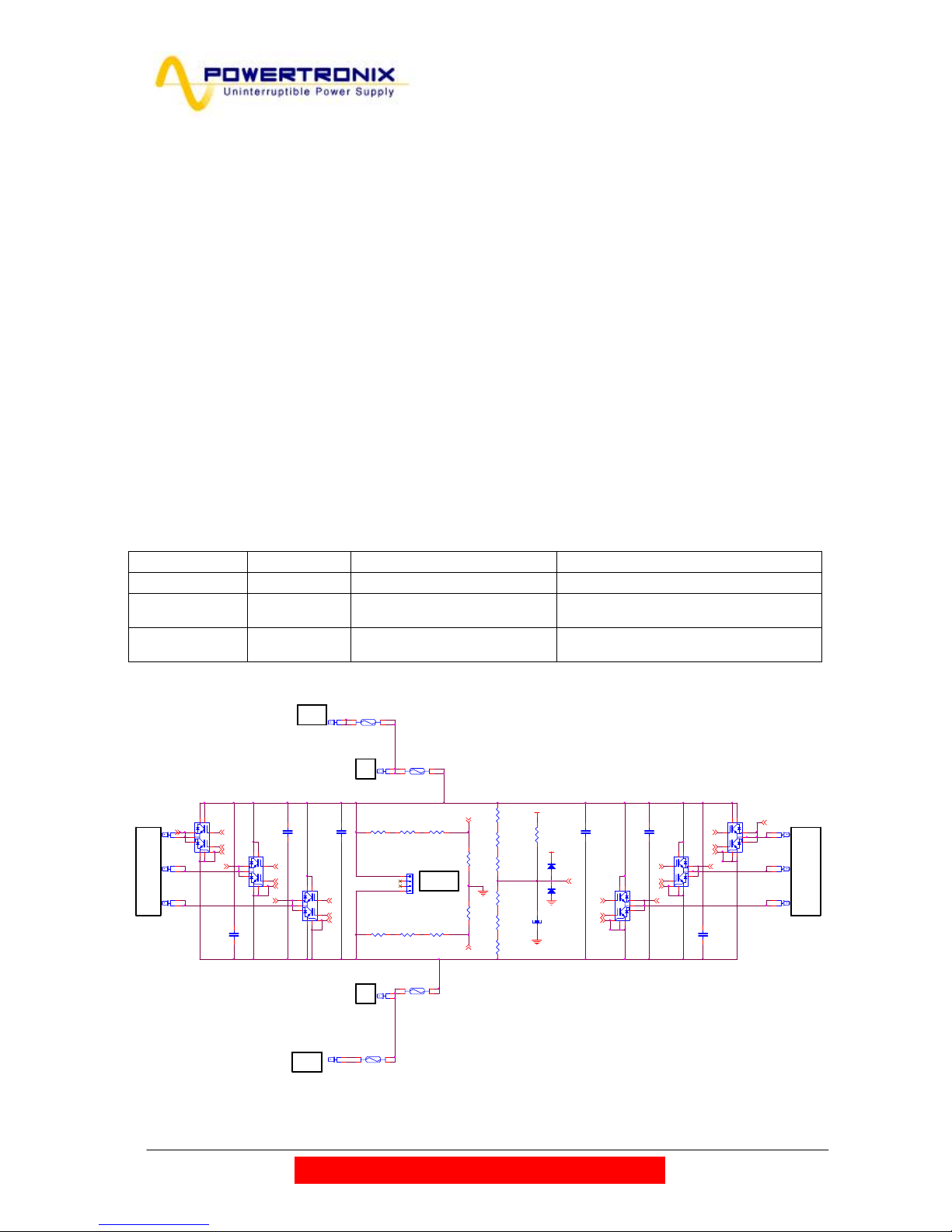
2 UPS COMPONENTS RECOGNIZING
To do servicing it’s necessary to recognize UPS parts , so , before troubleshooting ,
some pictures of UPS and parts will be shown in the following pages . To check pictures
it’s necessary to follow the UPS general schematic diagram (DE1244 and DE1245 )
attached at the end of this document .
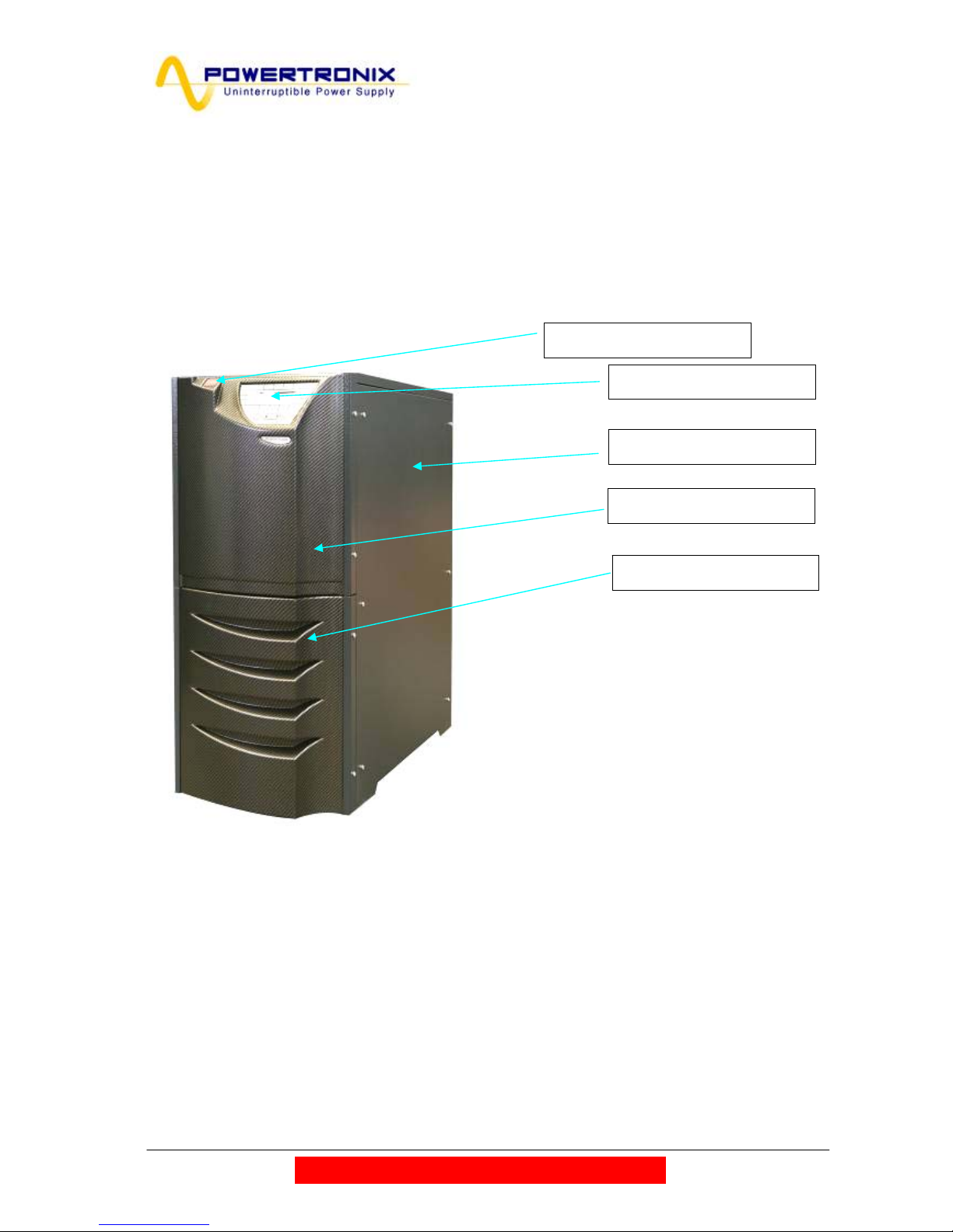
2.1 UPS CLOSED
Fig.1
*** WARNING !! Before removing safety covers after power disconnection , it’s
necessary to wait for 10 minutes to have discharged inner capacitors . In any case be
careful and never touch circuits or components before a voltage check
UPS Control Panel
UPS Side Cover panel
UPS Front Cover
BATTERY Front Cover
E:P:O: Command
R&D –SERVICE MANUAL DT0488
Powertronix spa reserves the right to modify this document without notice
Page. 7 of 72
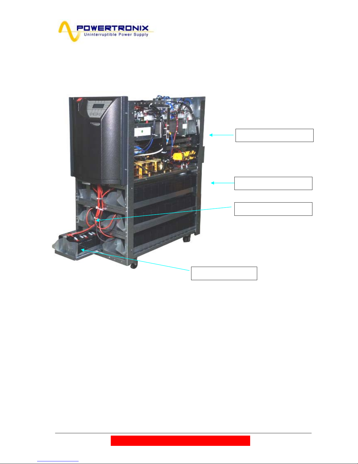
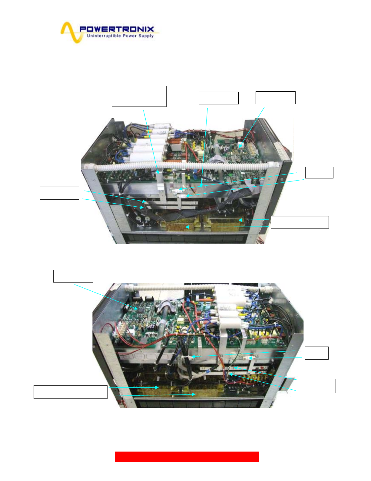
2.2 INNER VIEW WITH SAFETY COVER REMOVED
Fig.2
UPS Power Section
UPS Battery Location
BATTERY Connections
BATTERY String
R&D –SERVICE MANUAL DT0488
Powertronix spa reserves the right to modify this document without notice
Page. 8 of 72
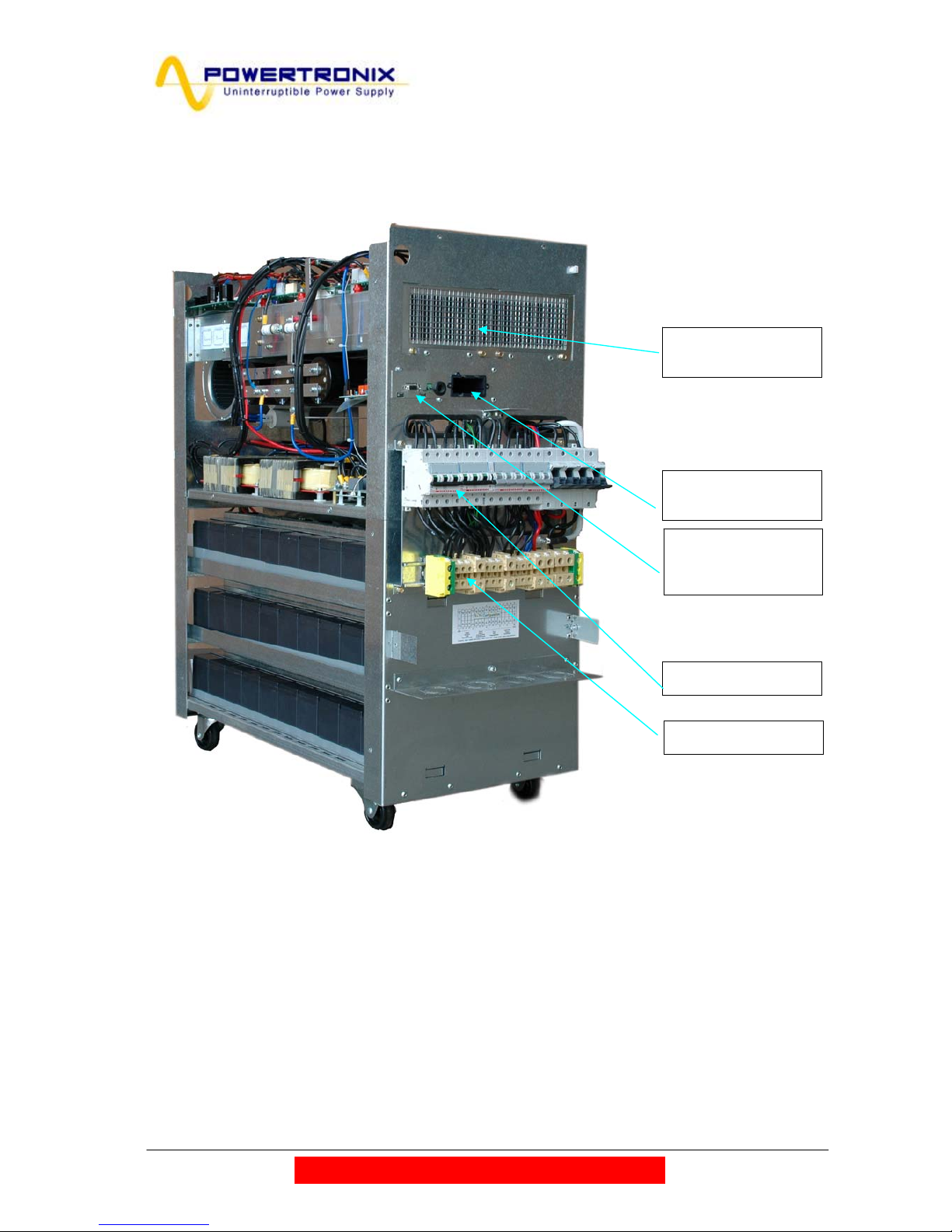
2.3 REAR UPS DESCRIPTION
Fig.3
Breaker
SNMP-Net Com
Slot location
RS232 & Status
Remote Control
Slot location
Output
Air window
Tagblock
R&D –SERVICE MANUAL DT0488
Powertronix spa reserves the right to modify this document without notice
Page. 9 of 72
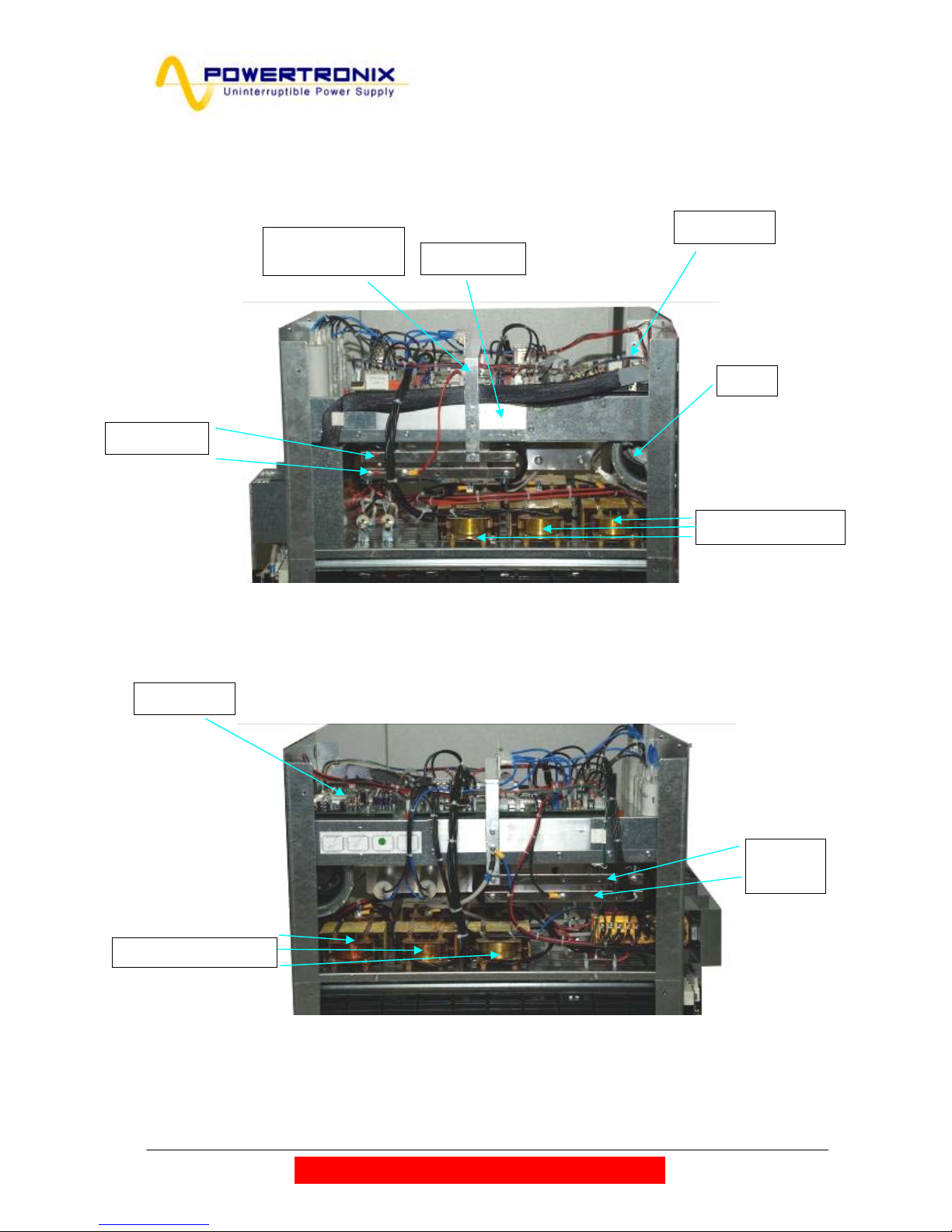
2.4 UPS-10-15KVA ELECTRONIC PARTS LAYOUT
LEFT SIDE
Fig.4
RIGHT SIDE
Fig. 5
NEUTRAL BAR
Connection
DC Busbar
HEATSINK
FAN
Power Impedence
DC
Busbar
Power Impedence
CS0150
CS0153
R&D –SERVICE MANUAL DT0488
Powertronix spa reserves the right to modify this document without notice
Page. 10 of 72
2.5 UPS-20-30KVA ELECTRONIC PARTS LAYOUT
LEFT SIDE
Fig. 6
RIGHT SIDE
Fig. 7
NEUTRAL BAR
CONNECTION
DC Busbar
HEATSINK
Power Impedence
DC Busbar
Power Impendence
Fuse
Fuse
CS0153
CS0150
R&D –SERVICE MANUAL DT0488
Powertronix spa reserves the right to modify this document without notice
Page. 11 of 72
2.6 UPS-10-15KVA BOARDS
This paragraph describes the PCB 's fitted in the UPS,
Subassembly code Description Diagram Circuit code
0sde 0150 Control Logic 7-30KVA DE0150 CS0150
0sde 0152 Inverter Drivers&Feedback Mizar DE0152 CS0152
0sde 0153 Aux. Converter DE0153 CS0153
0sde 0155 LCD Mimic Display "4*20" DE0155 CS0155
0sde 0143 Fuse Holder x 7-9 Ah DE0143 CS0143
0sde 0157 Fuse Holder x 7-9 Ah DE0157 CS0157
0sde 0154 H-F Filter DE0154 CS0161
0sde 0162 Temperature Sensor SMT DE0138 CS0138
0sde 0098 Relay Board DE0098 CS0098
2.7 UPS-20-30KVA BOARDS
This paragraph describes the PCB 's fitted in the UPS,
Subassembly code Description Diagram Circuit code
0sde 0150 Control Logic 7-30KVA DE0150 CS0150
0sde 0151 Inverter Drivers&Feedback Mizar DE0151 CS0151
0sde 0153 Aux. Converter DE0153 CS0153
0sde 0155 LCD Mimic Display "4*20" DE0155 CS0155
0sde 0143 Fuse Holder x 7-9 Ah DE0143 CS0143
0sde 0157 Fuse Holder x 7-9 Ah DE0157 CS0157
0sde 0161 H-F Filter DE0161 CS0161
0sde 0162 Temperature Sensor SMT DE0138 CS0138
0sde 0098 Relay Board DE0098 CS0098
0sde 0114 Fan Board DE0114 CS0114
R&D –SERVICE MANUAL DT0488
Powertronix spa reserves the right to modify this document without notice
Page. 12 of 72
2.8 BOARDS LAYOUT
2.8.1 UPS-10-15KVA Power Interface Board Component Layout
Refer to Electrical Diagram :DE0152
Fig. 8
Input
Precharge
Relay
Negative
DC Capacitor
Fuse
Negative
DC Battery Fuse
RESERVE
Relay
Static Switch
Positive
DC Batter
y
Fuse
Positive
DC Ca
p
acitor Fuse
IGBT
Input
Section
IGBT
Output
Section
INVERTER
Relay
Static Switch
R&D –SERVICE MANUAL DT0488
Powertronix spa reserves the right to modify this document without notice
Page. 13 of 72
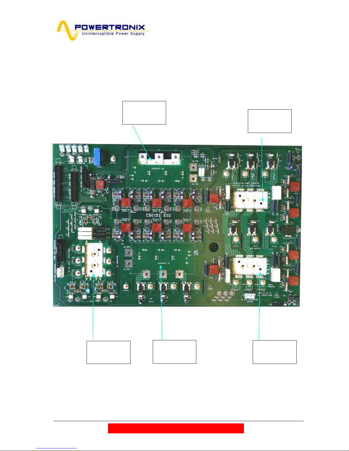
2.8.2 UPS-20-30KVA Power Interface Board Component Layout
Refer to Electrical Diagram :DE0151
Fig. 9
Input
Precharge
Thyristor
IGBT
INPUT
SECTION
RESERVE
Static Switch
Thyristor
IGBT
OUTPUT
SECTION
INVERTER
Static Switch
Thyristor
R&D –SERVICE MANUAL DT0488
Powertronix spa reserves the right to modify this document without notice
Page. 14 of 72
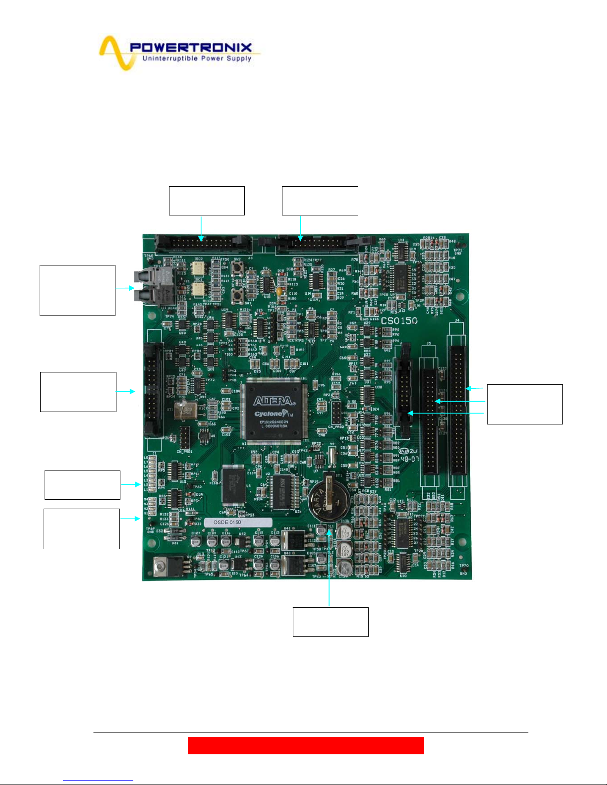
2.8.3 CS0150 UPS-10-15KVA UPS-20-30KVA CONTROL BOARD
Refer to Electrical Diagram :DE0150
Fig. 10
Fiber Optic
Connector
Parallel
Comunication
LCD Mimic
Display Board
Connectors
LED BAR
UPS STATUS
LED BAR
Processor
STATUS
Battery
Keep Timer
Interface
Board
Connectors
Relay Board
Connectors
SNMP
Connector
R&D –SERVICE MANUAL DT0488
Powertronix spa reserves the right to modify this document without notice
Page. 15 of 72
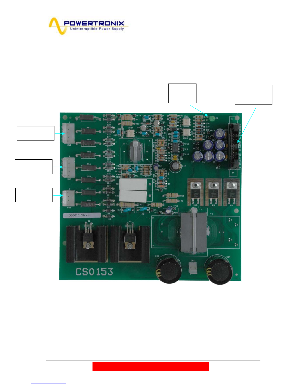
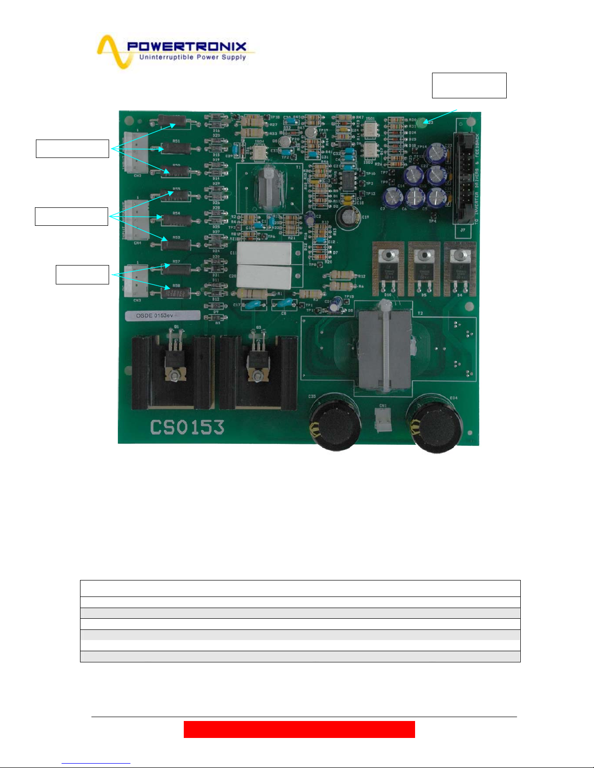
2.8.4 CS0153 UPS-10-15KVA UPS-20-30KVA POWER SUPPLY BOARD
Refer to Electrical Diagram :DE0153
Fig. 11
Input Mains
Connector
Input Reserve
Connector
DC Bus
Connector
Interface
Board
Connector
Power
Supply
status
R&D –SERVICE MANUAL DT0488
Powertronix spa reserves the right to modify this document without notice
Page. 16 of 72
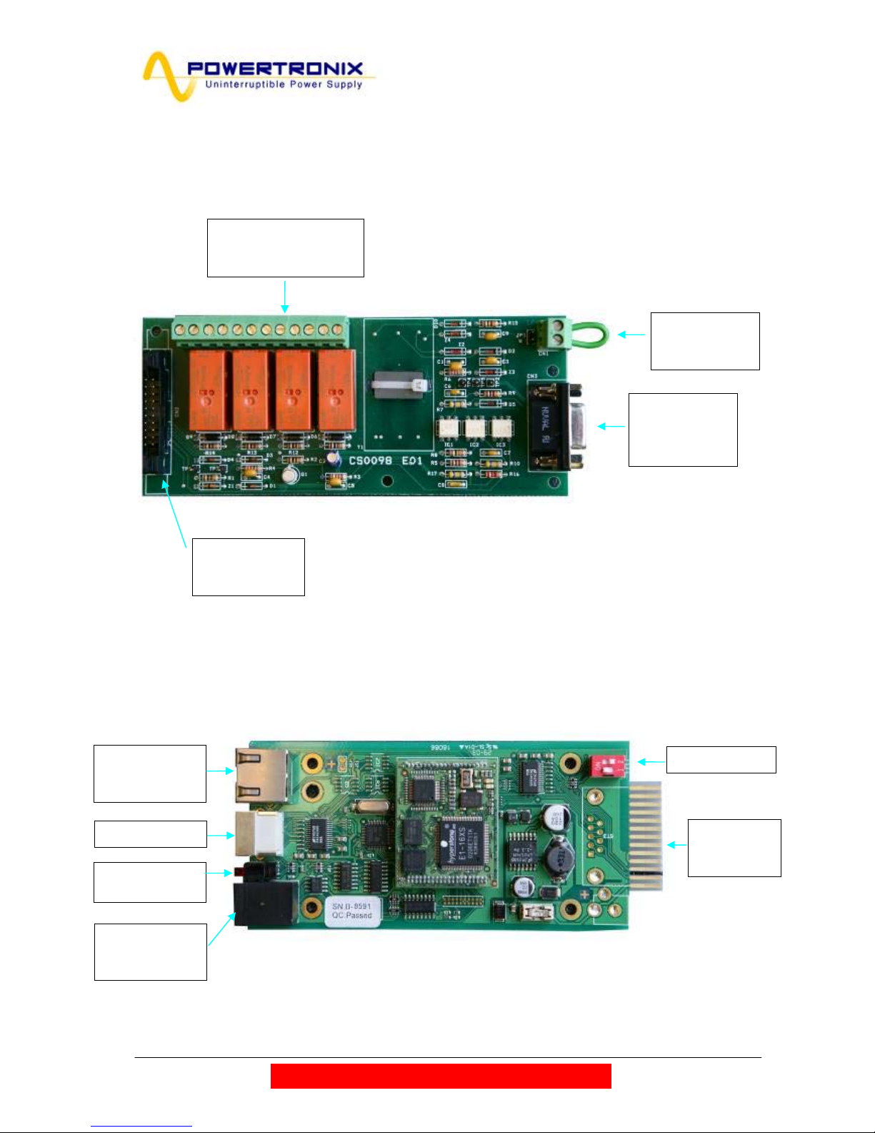
2.8.5 CS0098 RELAY & COMUNICATION BOARD
Refer to Electrical Diagram :DE0098
Fig. 12
2.8.6 SNMP COMUNICATION BOARD
Fig. 13
DB9
RS232
Comunication
Connector
E.P.O.
Terminal
Connection
FREE VOLTAGE
CONTACTS
UPS STATUS
CONTROL
LOGIC
CONNECTOR
Control
Logic
Connection
Config Switch
NET RJ45 +
status led
CONNECTOR
Serial Comport
Aux
Input/Output
Dr
y
contact
Status Led
Error Link
R&D –SERVICE MANUAL DT0488
Powertronix spa reserves the right to modify this document without notice
Page. 17 of 72
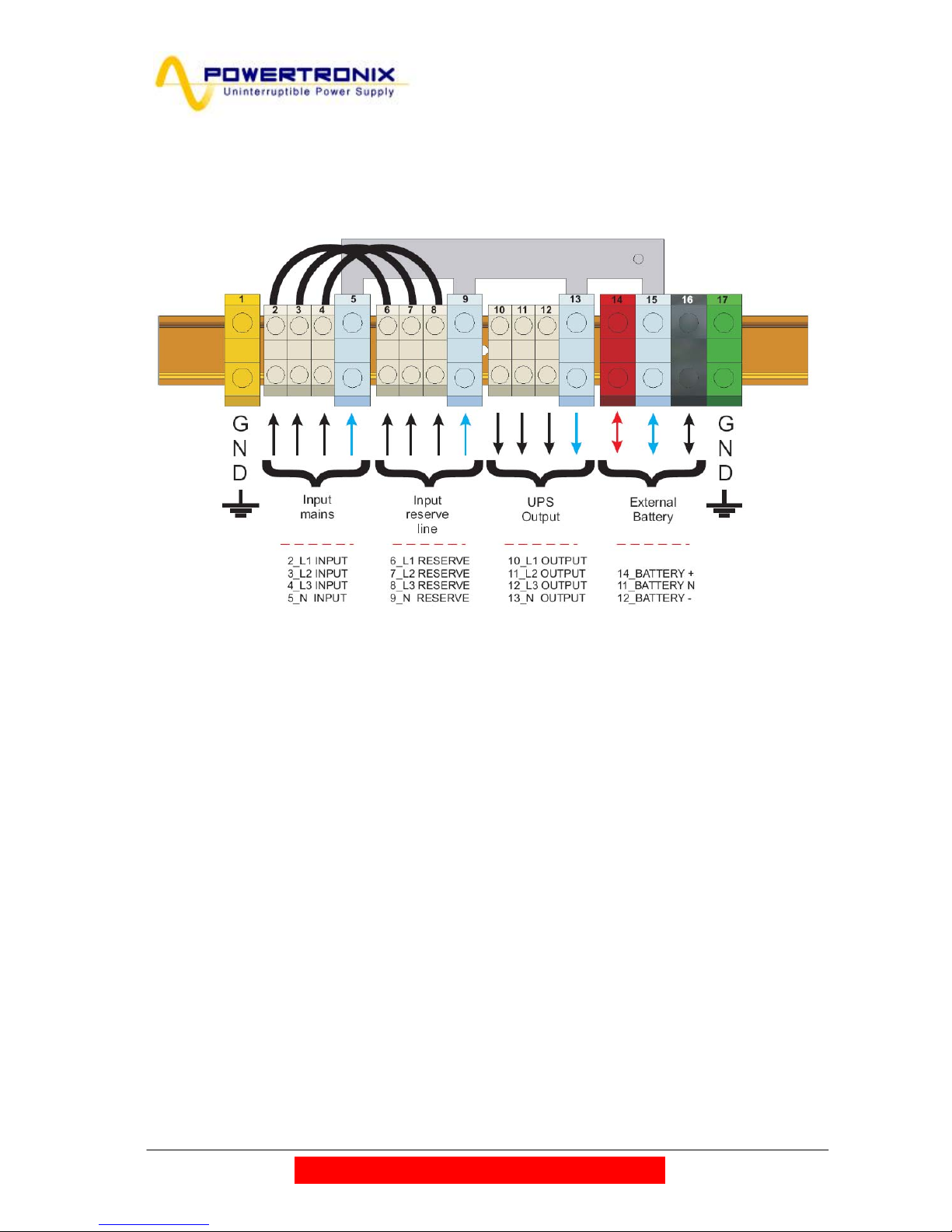
2.8.7 TERMINAL BLOCKS
Fig. 14
R&D –SERVICE MANUAL DT0488
Powertronix spa reserves the right to modify this document without notice
Page. 18 of 72
3 TROUBLESHOOTING
To identify a fault cause please refer to the following items.
3.1 POWER FUSE
F1-F2: Positive and Negative DC BUS.
F3-F4: Positive and Negative BATTERY
3.1.1 UPS-10-15KVA
Refer to Electrical Diagram :DE0152
Refer to Fig.8 UPS 10-15kVA Interface Board Component Layout
TAB.2
Fuse Value Protection of Location
F1-F2
32A
10x38mm
Battery Input
Power Interface BOARD (DE0152)
UPS 10-15kVA
F3-F4
32A
10x38mm
DC BUS
Power Interface BOARD (DE0152)
UPS 10-15kVA
SCH.2
P+5
P+5
E1-T
16_+DC-BUS
G3-T
E4-B
G1-T G4-T
E5-B
G5-T
G2-B
E3-B
G6-B
G4-BG1-B
E3-T E6-T
REF
16_-DC-BUS
G3-B
E5-T
G6-T
E2-B
G2-T
E6-B
G5-B
E4-T
E1-B
E2-T
AUX_CONV -DC
AUX_CONV +DC
FS6
L1
FS5
L2
FS22
L3
R183
100K 0.25W
R184
100K 0.25W
Q3
SK60GB128
28
6 13
27
2
1
24
125
23
F2
32A 10x38
1
2
3
4
C37
2.2µF PHB
850V
21
FS21
L2
Q6
SK60GB128
28
6 13
27
2
1
24
125
23
R180
150K 0.25W
R186
100K 0.25W
FS14
+ DC
R181
150K 0.25W
R188
150K 0.25W
C38
2.2µF PHB
850V
21
Q2
SK60GB128
28
6 13
27
2
1
24
125
23
C43
2.2µF PHB
850V
21
Q4
SK60GB128
28
6 13
27
2
1
24
125
23
R96
150K 0.25W
C40
2.2µF PHB
850V
21
R97
150K 0.25W
FS4
L3
C41
2.2µF PHB
850V
21
D42
1N4148
2 1
+
C62
10µF 16V
R187
100K 0.25W
F3
32A 10x38
1
2
3
4
Q1
SK60GB128
28
6 13
27
2
1
24
125
23
F1
32A 10x38
123
4
FS15
-DC
R185
100K 0.25W
F4
32A 10x38
1
2
3
4
D41
1N4148
2 1
R98
150K 0.25W
R99
6.8K
R100
6.8K
FS20
L1
R182
100K 0.25W
FS11
- BATTERY
R95
150K 0.25W
Q5
SK60GB128
28
6 13
27
2
1
24
125
23
FS10
+ BATTERY
CN3
DC BUS
1
2
3
4
C39
2.2µF PHB
850V
21
From Input
Inductor
To Aux.
Converter
CS0153
OUTPUT INVERTER
To Inverter
Inductor
INPUT INVERTER
Note the location of fuse are different in UPS 10-15kVA compare to UPS 20-30kVA
R&D –SERVICE MANUAL DT0488
Powertronix spa reserves the right to modify this document without notice
Page. 19 of 72
3.1.2 UPS-20-30KVA
Refer to Fig.6/7 UPS 20-30kVA LEFT/RIGHT SIDE electronic parts LAYOUT
TAB.3
Fuse Value Protection of Location
F1-F3 100A 690V
Positive Battery Input
Positive DC BUS
Right side Heatsink
UPS 20-30kVA
F2-F4 100A 690V
Negative Battery Input
Negative DC BUS
Left side Heatsink
UPS 20-30kVA
If you find one or more fuses blown, you have to check firstly
ALL the POWER semiconductors on the UPS
R&D –SERVICE MANUAL DT0488
Powertronix spa reserves the right to modify this document without notice
Page. 20 of 72
3.2 CHECK ALL PFC & INVERTER OUT IGBTS.
well locked . If IGBT is damaged , remember that probably the driver circuitry could be
damaged , so the following parts on interface board.
3.2.1 UPS-10-15KVA
CS 0152 have to be tested.
The following diagram detail regards only the driver circuitry for PFC L1 , only to indicate
the part of circuit .
Obviously also PFC L2&L3 and INVERTER L1&L2&L3 driver has to be tested.
SCH.3
P+15
P+15
HF supply 1
HF supply 2
DRV_L1-TOP_ING
DRV_L1-BOTT_ING
G1-T
E1-T
G1-B
E1-B
R4
1.8K
R10
270
R28
270
R19
1.8K
D4
UF4007
2 1
Z4
15V
2 1
+
C7
100µF 35V
TP1
D10
1N4148
2 1
T1
VAC4721X004
1
6
3
2
4
5
+
C1
100µF 35V
D13
1N4148
21
+
C16
100µF 35V
+
-
Totem
ISO4
HCPL3120
2
3
6
5 8
7
R13
1K
+
C10
100µF 35V
+
-
Totem
ISO1
HCPL3120
2
3
6
5 8
7
TP10
R22 33
Z10
P6KE18CAC250
2 1
R7 33
C4
1µF
D1
1N4148
2 1
Z1
P6KE18CAC250
2 1
D7
UF4007
2 1
TP4
Z7
15V
21
R16
1K
R1 33
TP7
R25
33
D16
1N4148
2 1
C13
1µF
INVERTER_IN PHASE L1
R&D –SERVICE MANUAL DT0488
Powertronix spa reserves the right to modify this document without notice
Page. 21 of 72
3.2.2 UPS-20-30KVA
CS 0151 have to be tested.
The following diagram detail regards only the driver circuitry for PFC L1 , only to indicate
the part of circuit .
Obviously also PFC L2&L3 and INVERTER L1&L2&L3 driver has to be tested.
SCH.4
P+15
P+15
HF supply 1
HF supply 2
DRV_L1-BOTT_ING
G1-T
E1-T
DRV_L1-TOP_ING
E1-B
G1-B
R10
270
R4
1.8K
R19
1.8K
R28
270
+
C7
100µF 35V
Z4
15V
2 1
D4
UF4007
2 1
D10
1N4148
2 1
TP1
+
C1
100µF 35V
T1
VAC4721X004
1
6
3
2
4
5
R13
1K
+
-
Totem
ISO4
HCPL3120
2
3
6
5 8
7
+
C16
100µF 35V
D13
1N4148
21
R22 10
TP10
+
-
Totem
ISO1
HCPL3120
2
3
6
5 8
7
+
C10
100µF 35V
Z10
P6KE18CAC250
2 1
D1
1N4148
2 1
C4
1µF
R7 10
Z7
15V
21
TP4
D7
UF4007
2 1
Z1
P6KE18CAC250
2 1
R25
10
TP7
R1 10
R16
1K
D16
1N4148
2 1
C13
1µF
INVERTER_IN PHASE L1
R&D –SERVICE MANUAL DT0488
Powertronix spa reserves the right to modify this document without notice
Page. 22 of 72
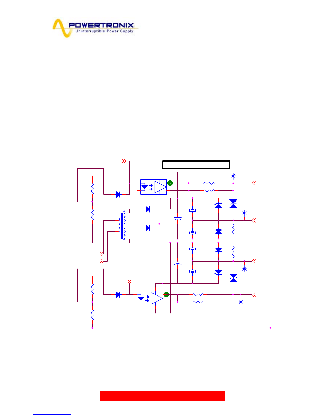
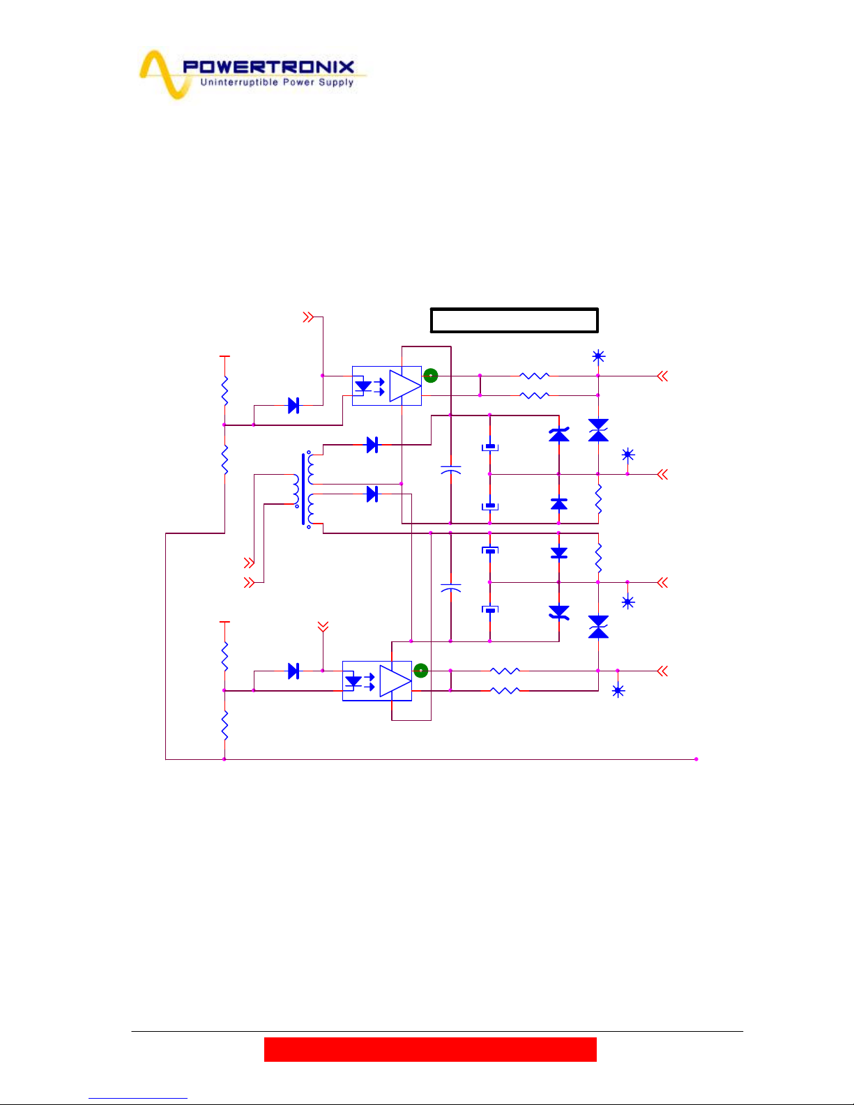
CS 0153 AUXILIARY DC/DC CONVERTER BOARD
Fig. 15
This board receives power from three different redundant sources :
800Vdc Voltage coming from DC bus ,
400V ac Voltage coming from Reserve ac input
400V ac Voltage coming from Mains ac input
These voltages, rectified are applied to a flyback dc/dc insulated converter that gives
regulated dc voltages on the output to all the boards of the UPS
Each line coming in are protected with resistor on the board.
Name Description Value Note
R57-R58 Positive and Negative DC input
47 ohm Fig.15
R50-R51-R52 Input Mains AC L1-L2-L3 input
47 ohm Fig.15
R53-R54-R55 Reserve Input AC L1-L2-L3 input
47 ohm Fig.15
LED D23
R57-R58
R50-R51-R52
R53-R54-R55

R&D –SERVICE MANUAL DT0488
Powertronix spa reserves the right to modify this document without notice
Page. 23 of 72
Output dc voltages status is monitored by a green Led D23 that have to be light while the
Power Supply is running
Name Description ON OFF
D23 Power Supply status P+15 Volt Output Present P+15 Volt Output not
Present
3.2.3 Check Auxiliary Power Supply Control Board
• 1-Check Input Voltage
1a-DC source Coming from DC BUS
(check between R57& R58 DC BUS Voltage >800Vdc)
1b-AC source Coming from AC Reserve Line
(check between R53 - R54 – R55 > 400Vac)
1c-AC source Coming from AC Mains Line
(check between R50 - R51 – R52 > 400Vac)
• 2-Check Output Voltage
3a-DC Output 7.5Volt dc
(check between TP7&TP9 DC Voltage ->7.5Vdc)
3b--DC Output 15Volt dc
(check between TP7&TP4 DC Voltage ->15Vdc)
3c--DC Output Isolated 15Volt dc
(check between TP14&TP12 DC Voltage ->15Vdc)
------------------------------------------------------------------------------------------------------------------Safe-Life Battery remote UPS’s location function
During battery discharging , the battery voltage is monitored by the control board ; when
the battery voltage reaches the minimum value the inverter is stopped ;
After few minutes (If SLB function is enabled) the control board sends an off command to
the dc/dc converter that switches off itself , avoiding the deep discharge of the UPS
battery .
The dc/dc converter turns automatically on when mains or reserve ac voltages come
back present .

R&D –SERVICE MANUAL DT0488
Powertronix spa reserves the right to modify this document without notice
Page. 24 of 72
CS0150 CONTROL LOGIC BOARD
Refer to Electrical Diagram :DE0150
Fig. 16
DL1= Green ON when Power supply 5Volt Volt is present
DL2= Yellow ON when Power supply 12Volt Volt is present
DL3= Green ON when Power supply 12 Volt is inside the right parameters
SW1=Push Button
SW2=Push Button
Upload STL Software Enable Function
LED BAR
UPS STATUS
LED BAR
Processor
STATUS
SW1-Button
Not Used
SW2-Button
Up-load
software micro
LED DL1-Green
Power Supply +5
Volt
Enabled
LED DL2-Yellow
Power Supply +12
Volt
Enabled
LED DL3-Green
Power Supply
+12 Volt
Enabled

R&D –SERVICE MANUAL DT0488
Powertronix spa reserves the right to modify this document without notice
Page. 25 of 72
Every control function of UPS depends by this board ,
Neither jumpers nor trimmers are employed for setting all UPS quantities on this board .
To change parameters it’s necessary to access to this board through the RS232 interface
communication board (CS0098) with a PC and follow the procedures described in
chapter 4.
No settings are needed , except when a new control board , not set in factory , has to be
placed in substitution of a faulty one.
Here is described meaning and localization of the LED present on the board
3.2.4 LED Status
On the control Logic you will find two LED BAR showing the status of the main block of
the ups.(Ref. to Fig.16 for localization)
Here you will find the meaning of each one.
The first BAR of LED L1-L6 shows the status of the Main blocks of the UPS.
The second BAR of LED M1-M4 show the status of the Microprocessor inside the control.
Name Colour Description ON OFF BLINKING
L1 Green Mains Line Status MAINS is OK Mains is not OK PFC-overload
L2 Green Battery Status Battery VOLT-OK Battery VOLT -NOK Battery-Prealarm
L3 Green Inverter Status RUNNING NOT RUNNING INV-overload
L4 Green Reserve Line Status Res. Line is OK Res. Line is not OK Phase-Rot. ERR
L5 Green PFC Status Battery-Charged PFC-NOT RUNN. Battery-In Charge
L6 Red Static Switch Status Load on Reserve Load on Inverter Load not Feed
L7 Yellow Normal Mode Synchro-OK Sync-Not Present X
L8 Green Parallel Status Master Slave X
M1
Yellow
M2
Yellow
M3
Yellow
M4
Red
Description
Blinking - - - µP normal operation
Blinking - - Blinking µP normal operation + memory writing. Do not switch off the power supply
- - - On µP update mode. Ready to receive the software "Standard"
Blinking Blinking - On µP update mode. Receiving the software "Standard"
Blinking Blinking Blinking On µP update mode. Verifying received software
On - - On µP update mode. Update error
- - - Blinking No valid software found. Ready to receive the software "Application"
On On On Blinking µP update mode. Erasing internal application memory
Blinking Blinking Blinking Blinking µP update mode. Receiving the software "Application"

R&D –SERVICE MANUAL DT0488
Powertronix spa reserves the right to modify this document without notice
Page. 26 of 72
3.2.5 Check Control Board
If at least one of the source input are available (reserve/Mains/Battery)is possible to
check the control Logic board
3.2.6 Check Power Supply Voltage
With references to electrical drawing DE 0150 check the following voltage-on the board
Name Description Test Point Value
P+15 Input Power Supply from CS0152
TP55-TP52 17.5Vdc
(15-20Vdc)
P+7.5 Input Power Supply from CS0152
TP61-TP58 7.5Vdc
(7.5-10Vdc)
P+12 Internal stabilized Power Supply
TP55-TP53 12Vdc
(11.75-12.25Vdc)
P+5 Internal stabilized Power Supply
TP61-TP59 5Vdc
(4.75-5.25Vdc)
P+3.3 Internal stabilized Power Supply
TP61-TP63 3.3Vdc
(3.1-3.5Vdc)
P+1.5 Internal stabilized Power Supply
TP61-TP65 1.5Vdc
(1.4-1.6Vdc)
N-7 Internal Power Supply
TP61-TP67 -7Vdc
(-6/-10Vdc)
P+12Delay Internal Power Supply Delay
TP61-TP54 12Vdc
After this control is possible to understand the status of the rest of the UPS connecting
the control board through the RS232 interface communication board with a PC and
follow the procedures described in chapter 4.

R&D –SERVICE MANUAL DT0488
Powertronix spa reserves the right to modify this document without notice
Page. 27 of 72
3.3 POWER INTERFACE UPS-10-15KVA BOARD
On this board are present all the electrical circuit used to adapt the level to the real used
from control, and all the actuators circuit used to drive the power parts present on UPS :
Here are described all the main component present on board (look figure 17 in the next
page):
Description N°
Ref.
Drawing
IGBT –L1 Input PFC 1 DE0152-Pag.2
IGBT –L2 Input PFC 2 DE0152-Pag.2
IGBT –L3 Input PFC 3 DE0152-Pag.2
IGBT –L1 Output INV 4 DE0152-Pag.2
IGBT –L2 Output INV 5 DE0152-Pag.2
IGBT –L3 Output INV 6 DE0152-Pag.2
Pre-charge Input section RELE 7 DE0152-Pag.2
SS-Switch Inverter Relay 8 DE0152-Pag.3
SS-Switch Reserve Relay 9 DE0152-Pag.3
Positive Battery Fuse Protection 10 DE0152-Pag.2
Positive DC Capacitors Fuse 11 DE0152-Pag.2
Negative DC Capacitors Fuse 12 DE0152-Pag.2
Negative Battery Fuse Protection 13 DE0152-Pag.2
Snubber Capacitors 14 DE0152-Pag.2
J4 50-pin Flat Cable Connector to Control Logic CS 0150 15 DE0152-Pag.4
J5 40-pin Flat Cable Connector to Control Logic CS 0150 16 DE0152-Pag.4
J7 20-pin Flat Cable Connector to Auxiliary Power Supply CS 0153 17 DE0152-Pag.4
CN9 2-Pin Molex Connector to Thermal Sensor “°C External Battery Box” 18 DE0152-Pag.4
CN7 2-Pin Molex Connector to Thermal Sensor “°C Internal Battery Box” 19 DE0152-Pag.4
CN6 2-Pin Molex Connector to Thermal Sensor “°C Heatsink” 20 DE0152-Pag.4
CN5 2-Pin Molex Connector “Not used” 21 DE0152-Pag.4
CN1 2-Pin Molex Connector to Over Temperature Protection 85°C 22 DE0152-Pag.4
CN10 2-Pin Molex Connector to “AUX Contact MANUAL BYPASS” 23 DE0152-Pag.2
CN11 2-Pin Molex Connector “Not used” 24 DE0152-Pag.2
CN2 5-Pin Molex Connector “Mains line to CS 0153” 25 DE0152-Pag.2
CN3 4-Pin Molex Connector “Feedback DC-BUS Voltage” 26 DE0152-Pag.2
CN4 5-Pin Molex Connector “Reserve line to CS 0153” 27 DE0152-Pag.3
F42 1A 250V Fuse protection for Fan 28 DE0152-Pag.2

R&D –SERVICE MANUAL DT0488
Powertronix spa reserves the right to modify this document without notice
Page. 28 of 72
UPS-10-15KVA Component Layout
Refer to Electrical Diagram :DE0152
Fig.17
1
2
3
4
5
6
7
8
9
10
11
12
13
14
15
16
17
18
19
20 21 22
23
24
25
26
27
28

R&D –SERVICE MANUAL DT0488
Powertronix spa reserves the right to modify this document without notice
Page. 29 of 72
3.4 POWER INTERFACE UPS-20-30KVA BOARDS (CS0151)
On this board are present all the electrical circuit used to adapt the level to the real used
from control, and all the actuators circuit used to drive the power parts present on UPS :
Here are described all the main component present on board:
Description N°
Ref.
Drawing
IGBT – Input PFC 1 DE0151-Pag.1
IGBT – Output INV 2 DE0151-Pag.1
Pre-charge Input section SCR 3 DE0151-Pag.2
SS-Switch Inverter SCR 4 DE0151-Pag.2
SS-Switch Reserve SCR 5 DE0151-Pag.2
J1 50-pin Flat Cable Connector to Control Logic CS 0150 6 DE0151-Pag.6
J4 40-pin Flat Cable Connector to Control Logic CS 0150 7 DE0151-Pag.6
J2 14-pin Flat Cable Connector to Control Logic CS 0150 8 DE0151-Pag.6
J3 20-pin Flat Cable Connector to Auxiliary Power Supply CS 0153 9 DE0151-Pag.6
CN11 2-Pin Molex Connector to Thermal Sensor “°C External Battery Box” 10 DE0151-Pag.6
CN9 2-Pin Molex Connector to Thermal Sensor “°C Internal Battery Box” 11 DE0151-Pag.6
CN8 2-Pin Molex Connector “Not used” 12 DE0151-Pag.6
CN7 2-Pin Molex Connector “Not used” 13 DE0151-Pag.6
CN6 2-Pin Molex Connector “Not used” 14 DE0151-Pag.6
CN5 2-Pin Molex Connector “Not used” 15 DE0151-Pag.4
CN4 2-Pin Molex Connector to “AUX Contact MANUAL BYPASS” 16 DE0151-Pag.4
CN1 4-Pin Molex Connector “Feedback DC-BUS Voltage” 17 DE0151-Pag.2
CN12 2-Pin Molex Connector “Second Speed Fan to CS 0114” 18 DE0151-Pag.4
CN2 5-Pin Molex Connector “Mains line to CS 0153” 19 DE0151-Pag.2
CN3 5-Pin Molex Connector “Reserve line to CS 0153” 20 DE0151-Pag.4

R&D –SERVICE MANUAL DT0488
Powertronix spa reserves the right to modify this document without notice
Page. 30 of 72
UPS-20-30KVA Interface Boards Component Layout
Refer to Electrical Diagram :DE0166 – DE0167 – DE0168
Fig.18
10
11
12 13 14
15
16
6
7
9
17
8
1
2
3
19
18
20
4
5

R&D –SERVICE MANUAL DT0488
Powertronix spa reserves the right to modify this document without notice
Page. 31 of 72
4 PC BASED CHECKS AND SETTINGS
As the UPS is equipped with LCD panel, most of basic operations can be done by the
user without using additional tools. Although, for the convenience and time save while
executing more complicated operations, the UPS logic control can be accessed also by
PC with dedicated UPS Maintenance UCT program.
This program is also the only way to modify some UPS parameters which are not
accessible through LCD panel.
Necessary things: PC with program installed, serial communication cable DB9-DB9 and
RS232 / Relay board CS0098 (standard on-board).
Below there is a short description of the program and its possibilities.
Few seconds after start, the program will be ready to use. The initial screen is similar to
the following picture:
As there is no standard way of using the program, the informations below contain just the
description of major functions. The user decides, which of them wants to use.
In most of cases it will be necessary to start the transmission between UPS and
computer. To do this, the user must define the serial port number and transmission
speed (usually 2400 bps),

R&D –SERVICE MANUAL DT0488
Powertronix spa reserves the right to modify this document without notice
Page. 32 of 72
and click on OK button. After this, program sends control data string to the UPS,
expecting correct response.
This process will be initiated automatically before any try of interaction between PC and
UPS, or can be involved manually by the user (menu Options > Communication mode).
Program remembers parameters (port number, speed, etc.) of last successful
transmission and uses them later as default settings.
Below there is description of main program functions.
Attention: all further explanations refers to the UPS-20-30KVA/ and R&D user access
level. Depending on the program version (R&D, service, user) some functions may be
hidden or disabled.
1. UPS identification button
Opens window containing UPS identification informations (model name, serial
number, firmware version, test date and service contact details). User can read all
the informations from the UPS or the backup file, modify them (except firmware
version) and write back to the UPS.
1
press

R&D –SERVICE MANUAL DT0488
Powertronix spa reserves the right to modify this document without notice
Page. 33 of 72
2. UPS configuration button
Opens window containing three tabs as described below:
• Main configuration tab
This tab contains essential UPS parameters: parallel mode and batteries
settings, output parameters (frequency, number of phases), and others.
• Nominal values tab
2
p
ress

R&D –SERVICE MANUAL DT0488
Powertronix spa reserves the right to modify this document without notice
Page. 34 of 72
"Nominal values" tab gives an access to some nominal UPS numeric
settings: output power and voltage, number of phases, battery parameters,
power factor and input/output frequencies.
• UPS Real Time Clock tab
This tab lets to control and change UPS internal clock and calendar
settings. The "Update from system" button serves for copying actual
computer time and date to the form.
With any tab, the user can read the informations from the UPS or from the file,
modify them and write back to the UPS.
The program operates (read / write operations) on the parameters which are
present on visible tab only.
3. UPS status and meters button
This button opens the window containing four different tabs, as described below.
All of them (except of the last one called "UDBS Obj.history") use the Idle read
mode to present actual UPS state and meters.
It means that the content of the "UPS status and meters" window is valid only when
the "Idle read" control is activated (green colour).
Otherwise, all the values in the window are not updated and becomes grey to
indicate inactive state.

R&D –SERVICE MANUAL DT0488
Powertronix spa reserves the right to modify this document without notice
Page. 35 of 72
• Main screen tab
This tab presents the mimic screen with the simplified diagram of the UPS
and 5 sections with values of measures. When the Idle read mode is active,
all the tab content is refreshed every second.
• UDBS object 2 to 9 tab
This tab gives an access to several informations available in UDBS
protocol. The user can choose from 1 to 6 different parameters from the
lists and watch them simultaneously. When the Idle read mode is active, all
the tab content is refreshed every second.
3
p
ress

R&D –SERVICE MANUAL DT0488
Powertronix spa reserves the right to modify this document without notice
Page. 36 of 72
• UDBS object 10 tab
With this tab user can observe several important internal UPS signals. It
can be useful in the case of UPS malfunction, servicing or maintenance.
As for the previous tabs, also this tab content is refreshed every second if
the Idle read mode is activated.
• UDBS object history tab
Using this tab user can download event log content from the UPS. Updated
log can be also saved to the file (button "Save to file" or File > Save UPS

R&D –SERVICE MANUAL DT0488
Powertronix spa reserves the right to modify this document without notice
Page. 37 of 72
history menu option). Unlikely to previous tabs, this one does not use Idle
read mode.
4. Commands and update button
This button opens the window containing two tabs, as described below.
• UPS commands tab
This tab contains several UPS commands, which can be useful while UPS
service or maintenance. To send the command to the UPS, the user should
choose the command and click "Execute command".
4
p
ress

R&D –SERVICE MANUAL DT0488
Powertronix spa reserves the right to modify this document without notice
Page. 38 of 72
• Software updates tab
"Software updates" tab allows changing the UPS firmware and/or LCD
panel language file, depending on the selected radio button. After clicking
on the "Open file" button, the user chooses the right update file, and the
program controls its content. If the file content is correct, the "Send update
to UPS" button will be enabled and ready to use.

R&D –SERVICE MANUAL DT0488
Powertronix spa reserves the right to modify this document without notice
Page. 39 of 72
5. Power/voltage button
This button opens the window with three tabs, containing important internal
numeric values of the UPS. Normally all the values are set correctly in the factory
and there is no need to modify them.
6. UPS setup button
This button opens "UPS setup" window, which contains some of the power/voltage
UPS values, used while performing unit setup process in the factory.
Except of the functions described above, the program allows creating the UPS backup
file (File > Save UPS backup option), saving Program Event Log, UPS History Log,
changing the interface language, supervising the transmission, etc.
5
p
ress

R&D –SERVICE MANUAL DT0488
Powertronix spa reserves the right to modify this document without notice
Page. 40 of 72
5 ELECTRICAL DIAGRAM
5.1 PCB electrical diagram index
- DE1237 UPS general diagram Mizar
- DE1112 UPS general diagram Alcor
- DE0098 Relay & Communication Board
- DE0138 Temperature sensor PCB
- DE0143 Battery Fuse PCB gap18mm
- DE0150 Control Logic
- DE0151 Inverter Driver & Feedback Alcor
- DE0152 Inverter Driver & Feedback Mizar
- DE0153 Power Supply Board
- DE0111 H-F Filter UPS 10-30kVA
- DE0155 LCD Mimic Display
- DE0157 Battery Fuse PCB gap22mm
- DE1235 Battery String

R&D –SERVICE MANUAL DT0488
Powertronix spa reserves the right to modify this document without notice
Page. 41 of 72
5.1.1 DE1237 UPS 10-15kVA general diagram
0SDE0178-A
EMC FILTER
PW21
PW22
PW23
PW24
PW2
PW3
PW4
PW5
PW20 PW1
Cabinet Temp
0SDE162
1
2
External Battery Temp
0SDE162
1
2
0SDE0178-B
EMC FILTER
PW25
PW26
PW27
PW28
PW7
PW8
PW6
PW9
PW18
0SDE0178-D
EMC FILTER
PW32
PW33
PW33
PW35
PW13
PW14
PW15
PW16
PW36PW17
Power Board and Feedback
0SDE0152
FS7
FS8
FS9
FS47
FS29
FS30
FS31
FS38
FS45
FS38
FS39
FS40
FS41
CN3
FS34
FS1
FS48
FS49
FS50
FS2
FS3
FS16
FS10
FS11
CN9[1..2]
J5[1..40]
J4[1..50]
CN6[1..2]
J7[1..20]
CN7[1..2]
FS6
FS23
FS4
FS5
FS28
FS25
FS20
FS21
FS22
CN2
CN4
CN9[1. .2]
CN5[1. .2]
CN1[1..2]
FS26
FS24
FS27
FS37
GND UPS
FS51
CN10[1. .2]
FS35
FS39
FS36
FS40
FS32
FS42
FS44
FS43
0SDE0153
AUX CONVERTER
CN2
CN4
J7[1..20]
CN3
CN1
0SDE0150
CONTROL LOGIC&SIGNALLING
J1[1..26]
J5[1..40]
J4[1..50]
J2[1..20]
J3[1..26]
0SDE0098
RELAY BOAR D
J2[1..20]
SNMP
J3[1..26]
0SDE0155
LCD BOARD
J1[1..26]
P9
10x(5-7-9Ah)
+
-
P11
10x(5-7-9Ah)
+
-
P7
10x(5-7-9Ah)
+
-
P12
10x(5-7-9Ah)
+
-
P10
10x(5-7-9Ah)
+
-
P8
10x(5-7-9Ah)
+
-
0SDE0178-C
EMC FILTER
PW29
PW30
PW12
PW10
PW31
PW11
Module Temp
0SDE162
1
2
NEUTRAL BAR
PW16
UPS_GND
N
UPS_GND
PW35
PW28, PW24, P W 30
CM1173
PW5, PW9, PW 11
UPS_GND
N
N
F4 F1
Neutral Breaker
I6
C1
40µF / 400-450V
L6
DSM191
VT1
0CEVTM2204P16W
I1
Input_Breaker
C2
40µF / 400-450V
L5
DSM191
L1
DSM191
C5
10µF / 400-450V
C9
10µF / 400-450V
C7
10µF / 400-450V
C8
10µF / 400-450V
P7
1
2
P10
1
2
P9
1
2
P8
1
2
P12
1
2
P11
1
2
P7
1
2
P8
1
2
P12
1
2
P10
1
2
P11
1
2
P9
1
2
C°
ST1
85°C
C3
40µF / 400-450V
CN10
MATLOK
123
4
I4
Output_Breaker
C6
10µF / 400-450V
L4
DSM191
L2
DSM191
L3
DSM191
Manual_By-Pass _Breaker
I3
20
22 21
24
19
23
123
4
C4
10µF / 400-450V
36 35
I2
Reserv e_Breaker
F3
32A
F2
32A
L1-BYPASS
L3-BYPASS
L2-BYPASS
- BATTERY
PHASE FAN
NEUTRAL FAN
AUX FAN
CM1293
31
6
7
345
29
8
33
40 - p1, 41 - p2
34
79 - 80
787776
75
16 17 18
15 15
19
22 21 20
15
23
12
15
24 25 26
27
15
13
15
73
74
14
31
31
UPS INPUT RESERVEEXT BATTERY
NEUTRAL BAR CM1173
NEUTRAL BAR CM1173
INPUT SECTION
INVERTER OUT SECTION
L1
L2
L3
N
L1
L2
L3
N
GND
+
-
Neutral
N
L2
UPS OUTPUT
L1
L3
GND
91011
28
32 32 32
353637
383940
414243
44
45
495051
525354
555657
46
4748
5859
2
3
4
7
10
11
12
14
16
6
12
34
65
78
910
11 12
21
221112910
CM1173
61 - 62 - 63
64 - 65 - 66
67 - 68
81 - 82
71 - 72
69 - 70
8
9
5
15
13
17
1
11
10987654
14 14 1313 1212 11
1
1312
23
1411
+ BATTER Y
30
To DC filter page 2|
FUSE
HOLDER_I5
FUSE
HOLDER_I5a
Aux_C o n tact

R&D –SERVICE MANUAL DT0488
Powertronix spa reserves the right to modify this document without notice
Page. 42 of 72
FS37
N - RES
FS45
N - RES
FS15
-DC
F3
32A 10x38
1
2
3
4
F2
32A 10x38
1
2
3
4
FS10
+ BAT
C9
10µF 400-450 V
FS35
L2
FS34
L3
FS36
L1
FS44
N
C7
10µF 400-450 V
C8
10µF 400-450 V
FS32
N
FS6
L1
FS4
L3
FS5
L2
FS48
L1
FS49
L2
FS50
L3
K4
9
8
7
1
2
6
5
4
F4
32A 10x38
1
2
3
4
F1
32A 10x38
1
2
3
4
FS40
L1 - RES
C6
10µF 400-450V
C5
10µF 400-450V
C4
10µF 400-450V
FS16
NEUTRAL
FS39
L2 - RES
FS38
L3 - RES
Q5
28
6 13
27
2
1
24
125
23
Q4
28
6 13
27
2
1
24
125
23
Q6
28
6 13
27
2
1
24
125
23
FS47
L3-OUT
FS11
- BAT
K5
9
8
7
1
2
6
5
4
FS7
L1 - IN
+
CE4
4400µF
450V
+
CE2
4400µF
450V
L3
DSM191
L2
DSM191
L1
DSM191
FS8
L2 - IN
FS9
L3 - IN
FS43
N - IN
FS25
L1
FS24
L2
FS23
L3
L4
DSM191
L5
DSM191
L6
DSM191
FS20
L1
FS28
L1
+
CE1
4400µF
450V
FS29
L1-OUT
FS31
L3-OUT
+
CE3
4400µF
450V
FS22
L3
FS21
L2
FS26
L3
FS27
L2
C3
40µF 400-450 V
C2
40µF 400-450 V
FS30
L2-OUT
C1
40µF 400-450 V
Q1
28
6 13
27
2
1
24
125
23
Q2
28
6 13
27
2
1
24
125
23
FS2
L2
FS3
L3
FS1
L1
Q3
28
6 13
27
2
1
24
125
23
FS14
+DC
R64
56R 10W
R63
56R 10W
R65
56R 10W
K1
735-3A-C-T SONG CHUAN
9
8
7
1
2
6
5
4
COMMON_NEUTRAL BAR
COMMON_NEUTRAL BAR
0SDE0152\B
PFC AND
INVERTER
SECTION
0SDE0152\C
S.SWITCH
SECTION
CM1181
CM1180
CM1180
CM1173
CM1181
CM1173
1
17
23
2
19
15
15
16
17
18
H3
H2
H1
Q1..Q3: SK60GB128 Q4..Q6: SK60GB128
0SDE0152\A
PRECHARGE
SECTION
31
15
15
22
21
20
H4
H5
H6 H10
H9
H8
30
18
18
27
28
29
15
16
K4, K5:
735-3A-C-T SONG CHUAN
2
1
65
10
9
3
4
7
8
11
12

R&D –SERVICE MANUAL DT0488
Powertronix spa reserves the right to modify this document without notice
Page. 43 of 72
5.1.2 DE1112 UPS 20-30kVA general diagram
0SDE0178
EMC FILTER
PW21
PW22
PW23
PW24
PW3
PW4
PW5
PW2
PW20 PW1
Trasduttore di temperat ura0
0SDE0162
2
1
0SDE0178
EMC FILTER
PW25
PW26
PW27
PW28
PW7
PW8
PW6
PW9
PW18
0SDE0161/D
EMC FILTER
PW32
PW33
PW34
PW35
PW13
PW14
PW15
PW16
PW36PW17
0SDE0151
Power Board and Feedback
PW4
PW5
PW6
FS12
PW14
PW15
PW16
FS15
FS9
PW23
PW22
PW21
FS13
CN3
FS14
L1 IGBT INV OUT
L2 IGBT INV OU T
L3 IGBT INV OU T
PW20
PW19
PW18
GND UPS
PW1
PW12
CN8[1..2]
J4[1..40]
J1[1..50]
CN11[1..2]
J3[1..20]
CN7[1..2]
PW7
PW9
PW8
PW25
PW26
PW27
FS4
FS5
FS6
CN2
FS10
CN9[1..2]
CN5[1..2]
CN6[1..2]
FS1
FS2
FS3
FS11
CN1
J2[1..14]
CN12[1..2]
CN4[1..2]
0SDE0114
FAN BOA RD
FS5
FS3
FS4
FS6
FS1
FS7
FS2
0SDE0098
RELA Y BOA RD
J2[1..20]
0SDE0153
AUX CON VERTER
CN2
CN4
J7[1..20]
CN3
CN1
0SDE0150
CONTROL L OGIC & SIGNALLING
J1[1..26]
J5[1..40]
J4[1..50]
J2[1..20]
J3[1..26]
J6[1..14]
0SDE0155
LCD BOA RD
J1[1..26]
SNMP
J3[1..26]
I553981
10x7Ah
+
-
I553977
10x7Ah
+
-
I553973
10x7Ah
+
-
I553985
10x7Ah
+
-
I553993
10x7Ah
+
-
I553989
10x7Ah
+
-
0SDE0178
EMC FILTER
PW29
PW31
PW30
PW10
PW12
PW11
Cabinet Temp.
0SDE0162
1
2
NEUTRAL BAR
UPS_GND
PW5, PW9, PW11
N
PW28, PW24, PW 30
PW16
UPS_GND
N
UPS_GND
CM1173
PW35
N
VT1
0CEVTM2204P16W
I1 63A
C8
10µF 400-450VC710µF 400-450V
L3
DSM192
L1
DSM192
C9
10µF 400-450V
L2
DSM192
I3 63A
C1
60µF 400-450V
C2
60µF 400-450V
I6 125A
C3
60µF 400-450V
AUX CONTACT
P1
1
2
P4
1
2
P2
1
2
P3
1
2
P5
1
2
P7
1
2
P6
1
2
P8
1
2
P9
1
2
P10
1
2
P12
1
2
P11
1
2
L3
DSM192
L1
DSM192
L2
DSM192
I5
F4 FUSE 50A
I5
F1 FUSE 50A
I5
F3 FUSE 50A
I5
F2 FUSE 50A
C5
10µF 400-450V
C4
10µF 400-450V
C6
10µF 400-450V
C°
ST1
85°C
I4 63A
I2 63A
L1-BYPASS
L3-BYPASS
L2-BYPASS
+ BATT ERY
- BATTERY
To DC filter page 2
AUX FAN
NEUTRAL FAN
PHASE FAN
COM
+
-
69
35 - p1, 36 - p2
L3L1L2
N
62 - 63 - 64
NEUTRAL BAR CM1173
EXT BATTERY
UPS OUTPUT
INVERTER OUT SECTION
INPUT SECTION
7
NCNCNC
CM1173
NEUTRAL BAR CM1173
CM1173
3°Floor
3 (Batt 1-) 874
2
1°Floor
1910
2°Floor
(Batt 2+)65
8
6
UPS INPUT
RESERVE
L2
N
L3
L3
NL2L1
L1
234
5
9
101112
13
141615
321
456
789
1213
14
15
161718
192021
22
23
24
101010
111111
25
26
29
28
31
27
32
30
30
30
30
34
30
30
36
35
37
38 39
404142
44 45
474849
505152
53
54
55
GND 17
GND 1
56
57
70
72
75 - 76
43
56
3
421
7
8
9
10
11
12
- ALCOR II Cod.0S 0195
WIRING
- BATTERY Cod. 0S0197
- INDUCTANCE Cod. 0S0191
59 - 60 - 61
68
67
71
73 - 74
77 - 78
65 - 66
79 - 80

R&D –SERVICE MANUAL DT0488
Powertronix spa reserves the right to modify this document without notice
Page. 44 of 72
L2L3L1
H2
ACS754
1
3
2
4 5
H1
ACS754
1
3
2
4 5
H3
ACS754
1
3
2
4 5
PW7
L1
PW9L3PW8
L2
PW27
L3
PW5
L2
PW6
L3
PW4
L1
C4 10µF 475V
C6 10µF 475V
C5 10µF 475V
+
CE4
4400µF
+
CE5
4400µF
+
CE6
4400µF
F1
100A
F2
100A
PW25
L1
F3
100A
PW12
- Batt
L5
L6
F4
100A
L4
S1
SCR SKUT85
3
5
1
2
4
6
7
101312
14
11
PW25
L1
PW26
L2
PW27
L3
PW1
+ Batt
PMB
2.5 µF
Q1
SEM iX201GD 128Ds
543
21
8
9
6
7
12
13
10
11
16
17
14
15
19
20
PMB
2.5 µF
Q2
SEMiX201GD128D s
543
21
8
9
6
7
12
13
10
11
16
17
14
15
19
20
+
CE2
4400µF
+
CE1
4400µF
+
CE3
4400µF
FS1
FS2
FS3
PW26
L2
Inverter IN
AC INPUT
CAPACITORS
INPUT MAINS
Inverter OUT
Neutral Bar CM 1 181
CM1448
CM1217
CM1173
CM1447
CM1216
CM1223
CM1444
CM1444
TO PAGE 3
Neutral Bar CM 1181
46
CM1173
CM1222 CM1449
850V 850V

R&D –SERVICE MANUAL DT0488
Powertronix spa reserves the right to modify this document without notice
Page. 45 of 72
PW21
L1-RES
PW22
L2-RES
PW23
L3-RES
H6
ACS754
1
3
2
54
C8
10µF 475V
C9
10µF 475V
C7
10µF 475V
H8
ACS754
1
3
2
4 5
H10
ACS754
1
3
2
4 5
H9
ACS754
1
3
2
4 5
FS11
FS12
FS9
L6
L5
L4
S2
SCR SKUT85
3
5
1
2
4
6
7
101312
14
11
R151
10 / 5W
C67
0.1µF MABA01
C69
0.1µF MABA01
C73
0.1µF MABA01
R155
10 / 5W
R156
10 / 5W
PW20
L3
S3
SCR SKUT85
3
5
1
2
4
6
7
101312
14
11
C2
60µF 450V
PW19L2PW18
L1
FS13
C1
60µF 450V
C3
60µF 450V
FS14
FS15
FS10
FS6
L3
FS4
L1
FS5
L2
C74
0.1µF MABA01
R157
10 / 5W
R158
10 / 5W
R159
10 / 5W
C76
0.1µF MABA01
C75
0.1µF MABA01
H5
ACS754
1
3
2
54
PW14
L1-OUT
PW15
L2-OUT
PW16
L3-OUT
H7
ACS754
1
3
2
54
FROM PAGE 2
Neutral Bar CM1173
Neutral Ba r CM 117 3
AC RESERVE
CAPACITORS
AC INVERTER
CAPACITORS
3430 30
45 44 43
30 3630
40 41 42

R&D –SERVICE MANUAL DT0488
Powertronix spa reserves the right to modify this document without notice
Page. 46 of 72
5.1.3 DE0098 Relay & Communication Board
P+15 P+15
P+15
P+15
P+15
P+15
P+15
P+15
IC1 4N35
1
2
5
4
6
R7
470K
C6
0.1nF50V
CN2
CON20
123456789
1011121314151617181920
D7
4007
D8
4007
D9
4007
R9 1K
R5 1K
TP2
M1
123456789
10
11
12
D6
4007
TP4
TP5
R6
2.7K
TP3
R12
100
TP1
R13
100
D5
1N4148
R14
100
T1
TRANSF OR MER F LAT 2+2
1
342 8
7
5
6
Z1
47V
C5
1µF
R3
1.2K
R2 100Q1
2N2222
R1 100
IC3 4N35
1
2
5
4
6
R17
470K
C80.1nF
50V
R15
1K
C7 1nF
50V
R11
100
K1
12V-12A
4
5
3
1
2
R4
22
C4
1µF
D1
1N4148
R8
10K
CN1
1
2
D2
1N4148
Z3
12VZ212V
R10
470K
K2
12V-12A
4
5
3
1
2
K3
12V-12A
4
5
3
1
2
D3
1N4148
K4
12V-12A
4
5
3
1
2
D4
1N4148
C1
1µF
C3
1µF
D10
1N4148
C9
1µF
Z4
12V
+
C2
10µF
CN3
DB9-FEMALE
594837261
JP1
IC2 4N35
1
2
5
4
6
R16
2.2K
A/C FAILURE
INVERTER
ONLOW
BATTERY
LOAD ON
AUTOMATIC BY-PASS
EPOA
EPOB
EPO
SER+12V
SER-12V
5 Turns
Coil
10 Turns
Coil
9 Turns
Coil
1 Turn
Coil

R&D –SERVICE MANUAL DT0488
Powertronix spa reserves the right to modify this document without notice
Page. 47 of 72
5.1.4 DE0138 Temperature sensor PCB
R1R4
C1
1uF 25V
J1
1
2
U1
LM334M
1
2
3
45
6
7
8
RESISTOR TABLE
R1 R4
18 ohm4.7 ohm 10µA\°K ALCOR\M I ZAR 0SDE0162
5.1.5 DE0143 Battery Fuse PCB (Battery 7.2-9Ah) / DE0157 Battery Fuse PCB
(Battery 4.5-5.2Ah)
FS4
FASTON-F
FS3
FASTON-F
FS2
FASTON-F
FS1
FASTON-F

R&D –SERVICE MANUAL DT0488
Powertronix spa reserves the right to modify this document without notice
Page. 48 of 72
5.1.6 DE0150 Control Logic
P+5P+3.3
UPS-LD3
UPS-LD6
UPS-LD7
UPS-LD5
UPS-LD2
UPS-LD1
UPS-LD4
DEBUG_LED1
DEBUG_LED2
DEBUG_LED3
DEBUG_LED4
UPS-LD8
L7
Yellow
21
L1
Green
21
L3
Green
21
L2
Green
21
L5
Green
21
L4
Green
21
RP3
470
1
2
3
45
6
7
8
U16C
ULN2003A
3 14
U16D
ULN2003A
4 13
U16B
ULN2003A
2 15
U16E
ULN2003A
5 12
U15A
ULN2003A
1 16
98
M3
Yellow
21
M2
Yellow
21
M1
Yellow
21
M4
Red
21
U15C
ULN2003A
3 14
U15B
ULN2003A
2 15
RP4
470
1
2
3
45
6
7
8
U15E
ULN2003A
5 12
U15D
ULN2003A
4 13
U15F
ULN2003A
6 11
RP6
470
1
2
3
45
6
7
8
RP5
470
1
2
3
45
6
7
8
RP1
470
1
2
3
45
6
7
8
U15G
ULN2003A
7 10
U16A
ULN2003A
1 16
98
RP2
470
1
2
3
45
6
7
8
L8
Green
21
L6
Red
21
DEBUG/STATUS LEDUPS-STATUS LED
OK
LD3 = INVERTER STATUS
MASTER \
SYNCRO OK
LOAD NOT FEEDLOAD ON RE S
BATTERY OK
OK
SLAVE \
SYNCRO NOK
FLOAT CHARG ELD5 = BATTERY CH ARG E R
RUN
BATT. DISCHARGE
ON
LD1 = MAINS STATU S
RX-. AL L \
X
LD4 = RES.LINE S T ATU S
BATT. PREALARMLD2 = BATT E RY STATU S
LD7 = PARALLEL STATUS
NORMAL MODE
INV.OVERLOAD
LD6 = STATIC-SW STATUS
X
OFF
OFF
PHASE ROTATIONNOK
BLINK
LOAD ON IN V
NOK
B.CH O F F
From Cyclone
BATT. FULL
LD8 = TEST TEST MODE PC COMM.X

R&D –SERVICE MANUAL DT0488
Powertronix spa reserves the right to modify this document without notice
Page. 49 of 72
P+3.3
P+3.3
P+3.3P+3.3P+3.3
P+3.3
EPO-REM
SPARE_1
BY-PASS_ON
SPARE_2
Sync ro
Synchro-Front
CN-EPO_LOCAL
EPO_LOCAL
PIO_0
CL_RESET
ENABLE _DC/DC
FAST-SPEED
REM_BYPASS_ON
REM_INVERTER_ON
REM_BATT_LOW
REM_ MAINS_NOK
OVER-85TMP_ALL
85TMP_ALL
MAINS_NOK
BYPASS_ON
INVERTER_ON
BATT_LOW
ENA _DC/DC
FAST-FAN
SPARE_ULN
CN_EPO-REM
AUX_BY-PASS_ON
CONTACT_SPARE_2
CONTACT_SPARE_1
TP1
U19B
ULN2003A
2 15
U18A
1 2
147
U19C
ULN2003A
3 14
R7
1M
C7
1µF
U19D
ULN2003A
4 13
C8
0.1µF
U19E
ULN2003A
5 12
R8 1M
C9
1µF
U18B
3 4
147
R9
100K
C5
1nF
R5 100K
C10
0.1µF
U17E
11 10
147
RP10
10K
1
2
3
45
6
7
8
SW2
PBswitch
13
SW1
RESET-CL
13
C1
1µF
U17A
1 2
147
R1
1M
RP7
10K
1
2
3
45
6
7
8
C6
0.1µF
RP8
470
1
2
3
45
6
7
8
C2
1µF
C3
1µF
R166
1K
U17D
9 8
147
C4
1µF
R4
100K
U19F
ULN2003A
6 11
U19G
ULN2003A
7 10
TP3
U18C
5 6
147
C11
0.1µF
R10
100K
TP7
TP5
TP2
TP9
TP4
TP6
U19A
ULN2003A
1 16
98
TP8
TP11
R3
100K
U17C
5 6
147
TP10
TP12
U17F
13 12
147
DZ3
24V
2 1
R6 1M
R159
1K
RP9
470
1
2
3
45
6
7
8
R2
1M
U17B
3 4
147
RELAYS COMMAND TO BOTH COMMUNICATION CARDS
WIRED-AND EPO SIGNALS
VL1-Rese rv e Line
To
Cyclone
From
Cyclone

R&D –SERVICE MANUAL DT0488
Powertronix spa reserves the right to modify this document without notice
Page. 50 of 72
REF_2.5V
REF_2.5V
REF_2.5V REF_2.5V
REF_2.5V
REF_2.5V
P+5
P+5
P+5
P+5
P+5
P+5
P+5
REF_2. 5V
REF_2. 5V
REF_2. 5VP+5
P+5
P+5
REF_2.5V
P+5
P+5
P+5
P+5
P+5
P+5
P+5
P+5
P+5
P+5
P+5
P+5
P+5
P+5
P+5
P+3.3
P+5 P+3.3
P+5
P+5
P+5 P+5
P+5
P+5
P+5
P+5
P+5 P+5 P+5
P+5
P+5
P+5
P+5
P+5 P+5
P+5 P+5
P+5
P+5
ANALOG-00
ANALOG-01
ANALOG-03
ANALOG-04
ANALOG-05
ANALOG-06
ANALOG-07
ANALOG-08
ANALOG-09
ANALOG-10
ANALOG-11
ANALOG-12
ANALOG-13
ANALOG-14
ANALOG-0202_V-INV_L3
ANALOG-07
ANALOG-08
ANALOG-06
07_V-MAINS_L2
08_V-MAINS_L3
12_V-OUT_L1 18_V-RES_L1
ANALOG-19
ANALOG-20
ANALOG-18
13_V-OUT_L2
14_V-OUT_L3
19_V-RES_L2
20_V-RES_L3
ANALOG-0303_A-INV_L1
04_A-INV_L2 ANALOG-04
ANALOG-0505_A-I NV_L3
09_A-MAINS_L1
ANALOG-09
10_A-MAINS_L2
ANALOG-10
11_A-MAINS_L3
ANALOG-11
21_A-OUT_L1 ANALOG-21
ANALOG-2222_A-OUT_L2
23_A-OUT_L3 ANALOG-23
ANALOG-16
16_+DC-BUS
ANALOG-1717_A-BATTERY
16_-DC-BUS
ANALOG-2424_MODULE_TEMP ANALOG-2525_INT-BATT_TEMP
ANALOG-26
06_V-MAINS_L1
ANALOG-13
ANALOG-14
ANALOG-12
ANALOG-17
ANALOG-18
ANALOG-19
ANALOG-20
ANALOG-21
ANALOG-22
ANALOG-23
ANALOG-24
ANALOG-25
ANALOG-26
ANALOG-27
000-A_MPX-0
000-B_MPX-0
000-C_MPX-0
000-D_MPX-0
000-A_MPX-1
000-B_MPX-1
000-C_MPX-1
000-D_MPX-1
000-INBT_-CS_0
000-SDATA_0
000-SCLK_0
000-INBT_-CS_1
000-SDATA_1
000-SCLK_1
ANALOG-02
ANALOG-16
ANALOG-0000_V-INV_L1
ANALOG-0101_V-INV_L2
ANALOG-28
26_EXT-BAT T_TEMP
27_I NVER TER_TEMP
28_PFC_TEMP
ANALOG-27
ANALOG-28
D27
1N4148
21
R19
82K
C20
10nF
R60
1K
R38
82K
C15
0,1µF
R57
1K
R173
1K
D19
1N4148
21
R36
82K
C36
10nF
TP36
TP22
R51
82K
R169
1K
D1
1N4148
2 1
C146
10nF
R165
1K
C40
1µF
R63
1K
D29
1N4148
C45
1µF
R70
1K
R61
1K
R170
1K
U9
HCF4067BM
1011141315
1
9876543
2
23222120191817
16
24
12
A
B
C
D
INBT
OUT
I0I1I2I3I4I5I6I7I8I9I10
I11
I12
I13
I14
I15
VCC
GND
R72
1K
TP24
C39
1µF
TP23
TP25
D18
1N4148
21
TP26
TP27
TP28
TP49
D24
1N4148
21
+
C136
100µF (10V)
TP39
TP38
C41
10nF
TP40
TP41
R66
1K
TP21
R49
82K
TP37
R73
1K
C46
10nF
D14
1N4148
21
R23
82K
R40
82K
R21
82K
U13
121S101
1
3 4
5
6
2
Vdd
Vin sclk
sdata
-cs
GND
R53
82K
C16
1µF
C37
10nF
C18
0,1µF
C19
0,1µF
R58
1K
U11
CD4504B
1234567
8
16
15
14
131211109
VCC
Aout
AinBout
BinCout
Cin
VSS
VDD
Fout
Fin
Sel
Eout
Ein
Dout
Din
R65
0 ohm
R64
NOT MOUNTED
R25
82K
R48
1K
C35
10nF
R42
82K
R55
82K
R171
1K
R30
10K
R31 10K
C24
0.1µF
C26
0.1µF
+
-
U14A
LM324
3
2
1
411
R28 10K
R27 22K
R29 22K
R67
1K
C42
10nF
+
C135
100µF (10V)
R12
2,2K
R11
470
R69
10M
R13
470
D2
1N4148
21
R74
1K
C47
10nF
R14
2,2K
U8
HCF4067BM
1011141315
1
9876543
2
23222120191817
16
24
12
A
B
C
D
INBT
OUT
I0I1I2I3I4I5I6I7I8I9I10
I11
I12
I13
I14
I15
VCC
GND
R172
1K
R15
3.3K
D16
1N4148
21
R20
470
C17
0,1µF
C38
10nF
R174
1K
R68
1K
C43
10nF
R59
1K
D17
1N4148
21
R75
1K
C48
10nF
D20
1N4148
21
TP14
R71
10M
R175
1K
TP15
TP16
D22
1N4148
21
TP17
R167
1K
TP19
TP18
R24
1K
TP20
R17
1K
C22
10nF
U10
CD4504B
1234567
8
16
15
14
131211109
VCC
Aout
AinBout
BinCout
Cin
VSS
VDD
Fout
Fin
Sel
Eout
Ein
Dout
Din
R41
1K
+
C134
100µF (10V)
R34
1K
R32
3.3K
R54
1K
C27
10nF
D23
1N4148
U12
121S101
1
3 4
5
6
2
Vdd
Vin sclk
sdata
-cs
GND
R46
1K
C29
10nF
R164
1K
C30
10nF
D6
1N4148
21
R56
1K
C34
10nF
R37
470
C33
10nF
R43
1K
R47
1K
D15
1N4148
21
R35
1K
TP29
R26
1K
C23
10nF
R18
1K
TP13
TP30
C145
10nF
D21
1N4148
21
R50
470
R62
1K
R44
3.3K
TP31
C31
10nF
C12
1µF
TP32
TP34
TP33
TP35
C14
0,1µF
C13
0,1µF
C25
0.1µF
D25
1N4148
21
D10
1N4148
21
D26
1N4148
21
C21
10nF
R33
1K
R22
1K
R16
1K
R45
1K
C28
10nF
R39
1K
R168
1K
C32
10nF
R52
1K
V-MAINS V-OUTPUT V-RESERVE
V BOOST FBK
DC-BUS
Temperatur e
HTSK-MODULE
Temperature
Battery
CABINET
Temperature
EXT-BATTER Y
Analog-04 = V-Inverter_L2
Corrispondenza Misure
Analog-27 = Temp.°C-Inverter IGBT
Analog-03 = V-Inverter_L1
Analog-31 = N.U.
Analog-02 = V-Inverter_L3
Analog-26 = Temp.°C-External Batt ery
Analog-30 = N.U.
Analog-01 = V-Inverter_L2
Analog 18 = V-Reserve_L1
Analog-29 = N.U.
Analog-00 = V-Inverter_L1
Analog-17 = A-DC Battery
Analog-25 = Temp.°C-Internal Battery
Analog-11 = A-Mains_L3
Analog-16 = V-DC bus
Analog-28 = Temp.°C- PFC IGBT
Analog-15 = N.U.
Analog-21 = A-Out_L1
Analog-24 = Temp.°C-Heatsink
Analog-14 = V-Out_L3
Analog-06 = V-Mains_L1
Analog-13 = V-Out_L2
Analog-20 = V-Reserve_L3
Analog-23 = A-Out_L3
Analog-05 = A-Inverter_L3
Analog-19 = V-Reserve_L2
Analog-22 = A-Out_L2
Analog-12 = V-Out_L1
Analog-10 = A-Mains_L2
Analog-09 = A-Mains_L1
Analog-08 = V-Mains_L3
Analog-07 = V-Mains_L2
V-INVERTER
Temperature
IGBT Inverter
30kVA
from NTC
Temperature
IGBT PFC
30kVA
from NTC
MONTATA AL
POSTO DI D3
1N4148
MONTATA AL
POSTO DI D4
1N4148
MONTATA AL
POSTO DI D5
1N4148
MONTATA A L
POST O DI D7
1N4148
MONTATA AL
POSTO DI D8
1N4148
MONTATA AL
POSTO DI D9
1N4148
MONTATA A L
POSTO DI
D11 1N4148
MONTATA AL
POSTO DI
D12 1N4148
MONTATA AL
POSTO DI
D13 1N4148

R&D –SERVICE MANUAL DT0488
Powertronix spa reserves the right to modify this document without notice
Page. 51 of 72
P+3.3
P+12_DELAY P+12_DELAY P+12_DELAY
P+12_DELAY
P+3.3
P+12_DELAYP+12_DELAY P+12_DELAY
P+3.3
P+12_DELAY
P+12_DELAY
P+12_DELAY
P+12_DELAY
P+12_DELAY
L1-TOP_INV
L2-BOTT_INV
L1-BOTT_INV
L3-BOTT_INV
L3-TOP_INV
L2-TOP_INV
DRV_L3-TOP_INV
DRV_L2-BOTT_INV
DRV_L1-BOTT_INV
DRV_L3-BOTT_INV
DRV_L1-TOP_INV
DRV_L2-TOP_INV
L1-BOTT_ING
L2-BOTT_ING
L3-TOP_ING
L1-TOP_ING
L2-TOP_ING
L3-BOTT_ING
DRV_L2-TOP_ING
DRV_L3-TOP_ING
DRV_L1-BOTT_ING
DRV_L3-BOTT_ING
DRV_L1-TOP_ING
DRV_L2-BOTT_ING
C54
0.1µF
Totem
U22B
ICL7667
4 5
18
C55
0.1µF
C56
0.1µF
Totem
U23B
ICL7667
4 5
18
C51
0.1µF
Totem
U23A
ICL7667
2 7
63
Totem
U24A
ICL7667
2 7
63
Totem
U24B
ICL7667
4 5
18
R82
100
R88
100
R86
100
R83
100
R84
100
R90
100
R81
100
R85
100
R89
100
R87
100
R91
100
Totem
U25B
ICL7667
4 5
18
Totem
U22A
ICL7667
2 7
63
R80
100
Totem
U25A
ICL7667
2 7
63
Totem
U26B
ICL7667
4 5
18
Totem
U27A
ICL7667
2 7
63
Totem
U27B
ICL7667
4 5
18
Totem
U26A
ICL7667
2 7
63
C52
0.1µF
RP12
470
1
2
3
45
6
7
8
RP13
470
1
2
3
45
6
7
8
RP14
470
1
2
3
45
6
7
8
C53
0.1µF
TP80
TP79
TP78
TP77
TP76
TP75
TP86
TP85
TP84
TP83
TP82
TP81
Input inverter (PFC)
IGBT commands
From
Cyclone
Output inverter
IGBT commands
From
Cyclone

R&D –SERVICE MANUAL DT0488
Powertronix spa reserves the right to modify this document without notice
Page. 52 of 72
P+3.3
P+3.3
P+12_DELAY
P+12_DELAY
P+12_DELAY
P+12_DELAY
P+12_DELAYP+12_DELAY
P+12_DELAY
P+12_DELAY
SS-RELE_RES
DRV_SS-RELE_RES
DRV_SS-RELE_INV
SS-INV_H F0
SS-INV_H F1
SS-BY_HF0
SS-BY_HF1
SS-RELE_INV
DRV_SS-BY_HF1
DRV_SS-BY_HF0
DRV_SS-INV_HF1
DRV_SS-INV_HF0
DRV_SCR_L3
DRV_Precharge-MAINS
DRV_SCR_L2
SCR_L2
Precharge-MAI NS
SCR_L3
DRV_SCR_L1
SCR_L1
Totem
U28A
ICL7667
2 7
63
Totem
U28B
ICL7667
4 5
18
R94
100
TP88
TP87
R92
100
Totem
U29A
ICL7667
2 7
63
Totem
U29B
ICL7667
4 5
18
R96
100
R98
100
TP90
TP89
R158
1K
C61
0.1µF
C60
0.1µF
Totem
U33B
ICL7667
4 5
18
Totem
U31A
ICL7667
2 7
63
Totem
U31B
ICL7667
4 5
18
R95
100
R93
100
R97
100
RP15
470
1
2
3
45
6
7
8
R156
1K
R157
1K
RP17
470
1
2
3
45
6
7
8
U38G
ULN2003A
7 10
98
U38F
ULN2003A
6 11
98
U38E
ULN2003A
5 12
98
TP98
TP97
TP96
C58
0.1µF
C57
0.1µF
Totem
U33A
ICL7667
2 7
63
From
Cyclone
Static Switch
SCR Commands
(20/30 kVA)
Static Switch
Relay
Commands
(7/15 kVA)
From
Cyclone
Precharge SCR
Commands
(20/30 kVA)
Precharge
Relay
Command
(7/15 kVA)

R&D –SERVICE MANUAL DT0488
Powertronix spa reserves the right to modify this document without notice
Page. 53 of 72
P+3.3P+3.3
P+3.3
P+3.3
P+3.3
P+3.3
P+3.3
P+3.3
P+3.3
P+3.3
P+3.3
P+3.3
CLK_IN
TDO
TCK
A4A3A2A1D0D1D3
D4
D5
A17
A16
A15
A14
A13
D7
D6
A5
A9
A10
A11
A12
A13
A14
D2
D12
D13
D14
D15
RAM_LBn
RAM_UBnA6RAM_OEnA8A7
D11
D10D9D8
A4A3A2A1D0D1D3
D4
D5
A19
A18
A17
A15
D7
D6
RAM_WEn
A5
D2
A16
A9
A10
A11
A12
D12
D13
D14
D15A6A8
A7
D11
D10D9D8
RAM_CEn
A6
A17
D13
D3
D9
A10
A2
A16
FLASH_WEn
A21
A19
D7
D12
A4
A14
A7
D2
A1
D6A20
D0
D11
A11
A12
D8
D5
FLASH_CEn
A8
A5
A15
D15
D1
D4
A9
D10
D14
A3
A13
FLASH_BYTEn
A18
FLASH_OEn
RAM_UBn
RAM_OEn
RAM_LBn
RAM_WEn
RAM_CEn
CLK_OUT
A19
A18
nCSO
TDI
TMS
nCE
DCLK
nCONFIG
ASDO
nSTATU S
CONF_DONE
DATA0
TMR_SC L
TMR_SD A
RP22
10K
1
2
3456
7
8
XT1
16.128.000 Hz
R104
5K6
C68
0.1µF
128Kx16bit
TSOP2-44pin
U2
BS616LV2010
123456789
10111213141516171819202122
444342414039383736353433323130292827262524
23
A4A3A2A1A0
CEn
DQ0
DQ1
DQ2
DQ3
VCC
GND
DQ4
DQ5
DQ6
DQ7
WEn
A16
A15
A14
A13
A12
A5A6A7
OEn
UBn
LBn
DQ15
DQ14
DQ13
DQ12
GND
VCC
DQ11
DQ10
DQ9
DQ8
NC
A8
A9
A10
A11
NC
CN_PRG2
10p-2.54
123456789
10
C65
1µF
RP19
10K
123
4 5
678
C63
1µF
TP42
U5
EPCS1
26
1
5
4
7
8
3
DATADCLK
NCS
ASDI
GND
VCC
VCC
VCC
RP20
10K
1
2
3
4 5
6
7
8
R105
1M
C66 33pF
R108 1K
C67 33pF R107 220
CN_PRG1
10p-2.54
123456789
10
BT1
3V Lithium
512Kx8bit
256kx16bit
U4 AM29LV400-TSOP48
123456789
101112131415161718192021222324
4847464544434241403938373635343332313029282726
25
A15
A14
A13
A12
A11
A10A9A8NCNC
nWE
nRESETNCNC
NY/nBYNCA17A7A6A5A4A3A2
A1
A16
nBYTE
VSS
DQ15/A-1
DQ7
DQ14
DQ6
DQ13
DQ5
DQ12
DQ4
VCC
DQ11
DQ3
DQ10
DQ2
DQ9
DQ1
DQ8
DQ0
nOE
VSS
nCE
A0
C69
1µF
RP21
1K
1
2
3
4 5
6
7
8
RP23
10K
1
2
3
4 5
6
7
8
512Kx16bit
TSOP2-44pin
U3 BS616LV8010
123456789
10111213141516171819202122
444342414039383736353433323130292827262524
23
A4A3A2A1A0
CEn
DQ0
DQ1
DQ2
DQ3
VCC
GND
DQ4
DQ5
DQ6
DQ7
WEn
A18
A17
A16
A15
A14
A5A6A7
OEn
UBn
LBn
DQ15
DQ14
DQ13
DQ12
GND
VCC
DQ11
DQ10
DQ9
DQ8
A8
A9
A10
A11
A12
A13
M41T00
U7
1
3
4
5627
8
OSCI
VBAT
VSS
SDA
SCLOSCO
FT/OUT
VCC
C64
1µF
Y2
32.768kHz
Byte-Blaster FPGA
programming
Byte-Blast er
EPCS1
programming
50maH
These two RAM are never mounted together. PCB footprints m ust be overlapping.
FPGA Programming Connector
Hardware Boot Memory Programming Connector
CPU Clock Crystal
System Calendar Clock
Male header
JTAG
connections:
pin# jtag
1 TCK
2 GND
3 TDO
4 Vcc
5 TMS
6 Vccio
7 (NC)
8 (NC)
9 TDI
10 GND
Output Test Frequency:
512Hz when Oscillator is
at 32.768KHz
Flash memory

R&D –SERVICE MANUAL DT0488
Powertronix spa reserves the right to modify this document without notice
Page. 54 of 72
P+3.3
P+3.3
P+12
P+12
P+12
P+12
P+12
P+12
BOTT1
BOTT2
BOTT3
BOTT4
CN-LCD_E
CN-LCD_RW
CN-LCD_RS
CN-T4
CN-T2
CN-T3
CN-T1
LCD_D0
LCD_D2
LCD_D3
LCD_D4
LCD_D5
LCD_D6
LCD_D7
LCD_D1
LCD_E
LCD_RW
LCD_RS
CN-LCD_D2
CN-LCD_D5
CN-LCD_D4
CN-LCD_D1
CN-LCD_D6
CN-LCD_D0
CN-LCD_D3
CN-LCD_D7
CN-LD2
CN-LD1
LD1
BUZZER
LD2
CN-BUZZER
CN-LCD_LIGHT_ON
LCD_LIGHT_ON
Totem
U48B
ICL7667
4 5
18
Totem
U44A
ICL7667
2 7
63
Totem
U49B
ICL7667
4 5
18
Totem
U44B
ICL7667
4 5
18
Totem
U49A
ICL7667
2 7
63
C71
0.1µF
U38A
ULN2003A
1 16
98
U38B
ULN2003A
2 15
98
U35D
40106
9 8
147
C70
0.1µF
U35B
40106
3 4
147
U35A
40106
1 2
147
U35C
40106
5 6
147
TP43
TP45
TP44
C77
0.1µF
RP30
470
123
4 5
678
RP29
470
123
4 5
678
RP28
470
123
4 5
678
C74
0.1µF
C78
0.1µF
RP24
10K
1
2
3
4 5
6
7
8
RP25
10K
123
4 5
678
DZ4
24V
2 1
Totem
U45A
ICL7667
2 7
63
Totem
U45B
ICL7667
4 5
18
TP93
TP
U38C
ULN2003A
3 14
98
Totem
U46A
ICL7667
2 7
63
Totem
U46B
ICL7667
4 5
18
Totem
U48A
ICL7667
2 7
63
Totem
U47A
ICL7667
2 7
63
Totem
U47B
ICL7667
4 5
18
BOTTONS FROM LCD BOARD
U38E, U38F, U38G
spostati a pag.5
to Cyclone
From
Cyclone

R&D –SERVICE MANUAL DT0488
Powertronix spa reserves the right to modify this document without notice
Page. 55 of 72
P+12
P+5
P+5
P+3.3
P+3.3
P+3.3
P+5
P+5
CN-SER_RX
CNSER_TX
SER_TX
ISO_N-15
CN-SNMP_SER_RX
ISO_P+15
ISO_P+15
CN-SNMP_SER_TX
ISO_N-15
SNMP_SER_T X
PAR-OPT_SER_TX
PAR-OPT_SER_RX
SER_RX
SNMP_SER_R X
R145
560
R144
560
R137
1K
TP74
R139
10K
TRX1
HFBR-1528
123
4
5
8
IC
nc
Vcc
Gnd
Vo
Gnd
Gnd
RX1
HFBR-2528
123
4
5 8
TP46
Totem
U50A
ICL7667
2 7
63
C137
0.1µF
TP47
TP51
R140
1K
TP50
U35E
40106
11 10
147
U35F
40106
13 12
147
R138
10K
C128
0.1µF
U39D
40106
9 8
147
R109 10K
C80
1nF
U39A
40106
1 2
147
C79
0.1µF
U38D
ULN2003A
4 13
98
U39E
40106
11 10
147
U39F
40106
13 12
147
R116
560K
R115 10K
R114
2.2K
R113
1K
R112
2.7K
R111
270
Q1
1
2
3
ISO2
4N35
1
2 4
6
5
R117
560K
Totem
U50B
ICL7667
4 5
18
U39B
40106
3 4
147
C84
1nF
D28
1N4148
2 1
C82
1nF
R142
1K
U39C
40106
5 6
147
ISO1
4N35
1
2 4
6
5
C83
1nF
R141
2.2K
R143
100
TP72
USER SERIAL INTERFACE
SNMP SERIAL INTERFACE
0.25 W
UPS PARALLEL SERIAL INTERFACE
from Cycloneto Cyclone

R&D –SERVICE MANUAL DT0488
Powertronix spa reserves the right to modify this document without notice
Page. 56 of 72
P+3.3 P+3.3 P+3.3P+3.3P+3.3P+3.3
P+3.3
P+3.3
P+1.5
P+3.3
P+1.5P+1.5P+1.5 P+1.5P+1.5P+1.5
P+3.3P+3.3 P+3.3P+3.3
P+1.5
P+3.3
P+1.5
P+1.5
P+1.5
P+1.5
P+1.5
P+1.5
nCONFI G
TDO
TDI
CLK_OUT
DATA0
UPS-LD3
DEBUG_LED1
UPS-LD6
DEBUG_LED2
UPS-LD7
UPS-LD5
DEBUG_LED3
UPS-LD2
UPS-LD1
DEBUG_LED4
Precharge-MAINS
EPO-REM
SPARE_1
SPARE_2
EPO_LOCAL
PIO_0
CL_RESET
85TMP_ALL
ENA _DC/D C
FAST-FAN
000-B_MPX-0
000-D_MPX-0
000-A_MPX-1
000-C_MPX-1
000-D_MPX-1
000-INBT_-CS _1
L3-BOTT_ING
L1-BOTT_ING
L2-BOTT_ING
L3-TOP_INV
L2-TOP_INV
SER_RX
HQ4
RUN
CONF_DONE
Sync hro-Front
000-SCLK_1
BOTT1
BOTT2
BOTT3
BOTT4
MAIN S_N OK
BATT_LOW
BYPASS_ON
PAR-OPT_SER_TX
PAR-OPT_SER_RX
A15
A14
A3A4A5
A6
A17
A18
A20
A8
A9
A10
A11
A12
D0D1D2D3D4D5D6
D8
D10
A7
A16
A1
L1-TOP_INV
LD1
LD2
BUZZER
LCD_E
LCD_RW
LCD_RS
UPS-LD8
000-INBT_-CS _0
A19
L1-TOP_ING
UPS-LD4 LCD_LIGH T_ON
SS-INV_HF0
SS-RELE_INV
SS-BY_HF0
RAM_OEn
RAM_LBn
RAM_WEn
TMR_S CL
FLASH_WEn
FLASH_BYTEn
FLASH_OEn
000-SCLK_0
D12
A21
SS-BY_HF1
000-SDATA_0
000-B_MPX-1
CLK_IN
SS-INV_HF1
SNMP_SER_RX
RAM_UBn
L2-BOTT_INV
INVERTER_ON
D7
D9
RAM_CEn
L3-BOTT_INV
A2
DCLK
A13
000-SDATA_1
SER_TX
L3-TOP_ING
SCR_L3
BY-PASS_ON
D11
TMR_S DA
000-A_MPX-0
225-TP_DBG4
TCK
ASDO
D13
nSTATUS
L2-TOP_ING
FLASH_CEn
L1-BOTT_INV
SCR_L1
nCE
SNMP_SER_TX
000-C_MPX-0
TMS
SPARE_ULN
SS-RELE_RES
LCD_D0
LCD_D1
LCD_D2
LCD_D3
LCD_D4
LCD_D5
LCD_D6
LCD_D7
nCSO
224-TP_DBG3
222-TP_DBG1
223-TP_DBG2
222-TP_DBG1
223-TP_DBG2
224-TP_DBG3
225-TP_DBG4
D14
D15
SCR_L2
C141
0.1µF
C142
0.1µF
IC
STD
ALTERA EP1C6 QFP 240
U1
EP1CC6Q240C7
112
92
70
172
157
130
231
209
189
51
22
9
154
27
150
31
151
30
232
230
212
210
192
190
171
142
129
111
109
91
89
71
69
52
40
10
240
239
1
144
143
38
39
238
237
236
235
234
233
226
225
224
223
222
221
220
219
218
217
216
199
198
197
196
195
188
187
186
185
184
183
182
181
332625
149
155
1473534
73
108
131
170
193
228
11
50
152
153
29
28
212019181716151413
12
87642
36
145332
146
24
148
37
107
93
74
176
156
127
194
208
227
5
23
55
72
90
110
191
211
229
616263646566676875767778798081828384858687889495969798
99
100
101
102
103
104
105
106
113
114
115
116
117
118
119
120
121
122
123
124
125
126
128
132
133
134
135
136
137
138
139
140
141
200
201
202
203
204
205
206
207
213
214
215
158
159
160
161
162
163
164
165
166
167
168
169
173
174
175
177
178
179
180
414243444546474849535456575859
60
VCCIO4
VCCIO4
VCCIO4
VCCIO3
VCCIO3
VCCIO3
VCCIO2
VCCIO2
VCCIO2
VCCIO1
VCCIO1
VCCIO1
VCCA_PLL2
VCCA_PLL1
GNDG_PLL2
GNDG_PLL1
GNDA_PLL2
GNDA_PLL1
GND
GND
GND
GND
GND
GND
GND
GND
GND
GND
GND
GND
GND
GND
GND
GND
GND
GND
DEV_CLRN
DEV_OE
INIT_DONE
PLL2_OUT1P
PLL2_OUT1N
PLL1_OUT0P
PLL1_OUT0N
IO_V2B2_16
IO_V2B2_15
IO_V2B2_14
IO_V2B2_13
IO_V2B2_12
IO_V2B2_11
IO_V2B2_10
IO_V2B2_9
IO_V2B2_8
IO_V2B2_7
IO_V2B2_6
IO_V2B2_5
IO_V2B2_4
IO_V2B2_3
IO_V2B2_2
IO_V2B2_1
IO_V2B2_0
IO_V0B2_12
IO_V0B2_11
IO_V0B2_10
IO_V0B2_9
IO_V0B2_8
IO_V0B2_7
IO_V0B2_6
IO_V0B2_5
IO_V0B2_4
IO_V0B2_3
IO_V0B2_2
IO_V0B2_1
IO_V0B2_0
NCE
NCONFIG
DATA0
TDO
TDI
TCK
MSEL1
MSEL0
DPCLK7
DPCLK6
DPCLK5
DPCLK4
DPCLK3
DPCLK2
DPCLK1
DPCLK0
CLK3
CLK2
CLK1
CLK0
IO_V0B1_14
IO_V0B1_13
IO_V0B1_12
IO_V0B1_11
IO_V0B1_10
IO_V0B1_9
IO_V0B1_8
IO_V0B1_7
IO_V0B1_6
IO_V0B1_5
IO_V0B1_4
IO_V0B1_3
IO_V0B1_2
IO_V0B1_1
IO_V0B1_0
DCLK
CONF_DONE
CLKUSR
NCEO
NSTATUS
NCSO
TMS
ASDO
VREF0B4
VREF1B4
VREF2B4
VREF0B3
VREF1B3
VREF2B3
VREF0B2
VREF1B2
VREF2B2
VREF0B1
VREF1B1
VREF2B1
VCCINT
VCCINT
VCCINT
VCCINT
VCCINT
VCCINT
IO_V2B4_0
IO_V2B4_1
IO_V2B4_2
IO_V2B4_3
IO_V2B4_4
IO_V2B4_5
IO_V2B4_6
IO_V2B4_7
IO_V2B4_8
IO_V2B4_9
IO_V2B4_10
IO_V2B4_11
IO_V2B4_12
IO_V2B4_13
IO_V2B4_14
IO_V2B4_15
IO_V2B4_16
IO_V2B4_17
IO_V2B4_18
IO_V1B4_0
IO_V1B4_1
IO_V1B4_2
IO_V1B4_3
IO_V1B4_4
IO_V1B4_5
IO_V1B4_6
IO_V1B4_7
IO_V1B4_8
IO_V1B4_9
IO_V1B4_10
IO_V0B4_0
IO_V0B4_1
IO_V0B4_2
IO_V0B4_3
IO_V0B4_4
IO_V0B4_5
IO_V0B4_6
IO_V0B4_7
IO_V0B4_8
IO_V0B4_9
IO_V0B4_10
IO_V0B4_11
IO_V0B4_12
IO_V2B3_0
IO_V2B3_1
IO_V2B3_2
IO_V2B3_3
IO_V2B3_4
IO_V2B3_5
IO_V2B3_6
IO_V2B3_7
IO_V2B3_8
IO_V2B3_9
IO_V2B3_10
IO_V2B3_11
IO_V2B3_12
IO_V2B3_13
IO_V2B3_14
IO_V2B3_15
IO_V2B3_16
IO_V1B2_0
IO_V1B2_1
IO_V1B2_2
IO_V1B2_3
IO_V1B2_4
IO_V1B2_5
IO_V1B2_6
IO_V1B2_7
IO_V1B2_8
IO_V1B2_9
IO_V1B2_10
IO_V0B3_0
IO_V0B3_1
IO_V0B3_2
IO_V0B3_3
IO_V0B3_4
IO_V0B3_5
IO_V0B3_6
IO_V0B3_7
IO_V0B3_8
IO_V0B3_9
IO_V0B3_10
IO_V0B3_11
IO_V0B3_12
IO_V0B3_13
IO_V0B3_14
IO_V0B3_15
IO_V0B3_16
IO_V0B3_17
IO_V0B3_18
IO_V2B1_0
IO_V2B1_1
IO_V2B1_2
IO_V2B1_3
IO_V2B1_4
IO_V2B1_5
IO_V2B1_6
IO_V2B1_7
IO_V2B1_8
IO_V2B1_9
IO_V2B1_10
IO_V2B1_11
IO_V2B1_12
IO_V2B1_13
IO_V2B1_14
IO_V2B1_15
C144
0.1µF
C99
0.1µF
C98
0.1µF
C92
0.1µF
C91
0.1µF
R160
1K
C96
0.1µF
C97
0.1µF
C93
0.1µF
C94
0.1µF
C95
0.1µF
R163
1K
R1621KR161
1K
C139
0.1µF
TP100
TP95
TP94
TP56
C101
0.1µF
C100
0.1µF
C104
0.1µF
C103
0.1µF
C102
0.1µF
C140
0.1µF
C90
0.1µF
C143
0.1µF
C88
0.1µF
C89
0.1µF
C86
0.1µF
C87
0.1µF
C85
0.1µF

R&D –SERVICE MANUAL DT0488
Powertronix spa reserves the right to modify this document without notice
Page. 57 of 72
P+12
P+5
P+3.3
P+1.5
P+15
P+5
P+5
P+7.5
P+12
P+15P+5
P+7.5
P+15
P+5
P+12 P+12_DELAY
P+5
P+12
N-7
HQ4
RUN
N-7
N-7
TP70
R150
10M
D39
1n4148
2 1
TP71
U18F
13 12
14 7
+
-
U14D
LM324
12
13
14
4 11
+
-
U14B
LM324
5
6
7
4 11
U16G
ULN2003A
7 10
TP58TP62TP64
TP59TP63TP65
TP67
U18E
11 10
14 7
U18D
9 8
147
U16F
ULN2003A
6 11
TP52
+
-
U14C
LM324
10
9
8
4 11
+
C109
10µF35V
DZ5
3.9V
2 1
TP53
DZ8
6.2V
21
C119
0.1µF
R124
1K
R123
1K
U40 7812
1 3
2
IN OUT
REF
TP61
+
C120
10µF 35V
DL3
Green
21
C123
0.1µF
U43
NCP1117DT15
3 2
1
IN OUT
REF
DL1
GREEN
21
R131
680
R134
1K
R125
1K
+
C121
10µF 35V
C122
0.1µF
C117
0.1µF
+
C111
10µF 35V
+
C115
10µF 35V
+
C116
10µF 35V
C118
0.1µF
DL2
YELLOW
21
C113
0.1µF
Q2 BDX54
1
23
U41 7805
1 3
2
IN OUT
REF
U42
LM2937IMP3.3
1 3
2
4
+
C105
10µF 35V
C114
0.1µF
R135
2.2K
+
C112
10µF 35V
C108
0.1µF
D37
1n4148
2 1
TP55
R120
10K
+
C106
10µF 35V
R119
560
C107
0.1µF
C110
1µF
D38
1n4148
21
R122
1.2K
R118
1K
D31
UF4007
21
R121
560
D32
UF4007
21
R132
1K
R133
1K
+
C127
10µF35V
C126
1µF
TP57
TP60
TP54
D34
1n4148
2 1
TP68
R146
470
TP69
DPAK
D2PAK
D2PAK
SOT223
distribuiti
sulla scheda
scrivere
simbolo di
massa
POWER SOURCE TEST LED
1=RUN t o EP LD
0=pow-OK
Sorveglianza PSP OK
(+15V e +7.5V)

R&D –SERVICE MANUAL DT0488
Powertronix spa reserves the right to modify this document without notice
Page. 58 of 72
P+15
P+5
P+5
P+5
P+7.5
P+7.5
P+15
P+15
P+5
P+5
P+5
P+5
P+5
P+7.5
CN-LCD_D5
CN-T2
CN-LCD_D1
CN-LCD_E
CN-LCD_D7
CN-LCD_RW
CN-LCD_D0
CN-LCD_D2
CN-LCD_RS
CN-LCD_D3
CN-LD2
CN-T1
CN-T4
CN-LCD_D6
CN-BUZZER
CN-T3
CN-LD1
CN-EPO_LOCAL
CN-LCD_D4
CN-SNMP_SER_RX
CN-SNMP_SER_TX
CN_EPO-REM
CN-SER_RX
REM_MAI NS _NOK
REM_BYPASS_ON
REM_INVERTER_ON
REM_BATT_LOW
CNSER_TX
DRV_SS-BY_HF1
DRV_SS-INV_HF0
DRV_SCR_L3
16_+DC-BUS
26_EXT-BATT_TEMP
25_INT-BATT_TEMP
24_MODULE_TEMP
17_A-BATTERY
16_-DC-BUS
23_A-OUT_L3
21_A-OUT_L1
22_A-OUT_L2
05_A-INV_L3
03_A-INV_L1
04_A-INV_L2
11_A-MAINS_L3
DRV_SS-INV_HF1
10_A-MAINS_L2
09_A-MAINS_L1
13_V-OUT_L2
14_V-OUT_L3
12_V-OUT_L1
02_V-INV_L3
00_V-INV_L1
01_V-INV_L2
19_V-RES_L2
20_V-RES_L3
18_V-RES_L1
08_V-MAINS_L3
07_V-MAINS_L2
06_V-MAINS_L1
DRV_SS-BY_HF0
ISO_N-15
CONTACT_SPAR E_2
DRV_L2-TOP_ING
DRV_SS-RELE_R ES
OVER-85TMP_ALL
DRV_L1-TOP_INV
DRV_L2-BOTT_ING
DRV_SS-RELE_INV
DRV_L3-TOP_ING
DRV_Precharge-MAINS
DRV_L3-TOP_INV
DRV_L1-BOTT_ING
ENABLE _DC/DC
ISO_N-15
ISO_P+15
ISO_P+15
FAST-SPEED
DRV_L3-BOTT_INV
DRV_L3-BOTT_ING
DRV_L1-BOTT_INV
ISO_N-15
AUX_BY-PASS_ON
DRV_L2-TOP_INV
DRV_L2-BOTT_INV
DRV_L1-TOP_ING
ISO_P+15
Syncro
CN-LCD _LIGHT_ON
DRV_SCR_L2
DRV_SCR_L1
27_INVERTER_TEMP
28_PFC_TEMP
CONTACT_SPARE_1
J5
CON40
1
2
3
4
5
6
7
8
9
10
11
12
13
14
15
16
17
18
19
20
21
22
23
24
25
26
27
28
29
30
31
32
33
34
35
36
37
38
39
40
J3
CON26
1
2
3
4
5
6
7
8
9
10
11
12
13
14
15
16
17
18
19
20
21
22
23
24
25
26
J4
CON50
1
2
3
4
5
6
7
8
9
10
11
12
13
14
15
16
17
18
19
20
21
22
23
24
25
26
27
28
29
30
31
32
33
34
35
36
37
38
39
40
41
42
43
44
45
46
47
48
49
50
C129
1µF
C130
1µF
C131
1µF
C132
1µF
J6
CON14
1
2
3
4
5
6
7
8
9
10
11
12
13
14
J2
CON20
1
2
3
4
5
6
7
8
9
10
11
12
13
14
15
16
17
18
19
20
J1
CON26
1
2
3
4
5
6
7
8
9
10
11
12
13
14
15
16
17
18
19
20
21
22
23
24
25
26
Connettore LCD
DB2
DB7
DB5
DOWN-Back
DB0
BUZZER
DB1
DB6
DB4
LD1
Clear
R/W
LD2
Home
EN
DB3
EPO
RS
UP-Next
Connettore SERIALE RELE CONTATTI Connettore SNMP-BOX
to SNMP BOX
MAINS FAILURE
RX
TX
EPOA
BATTER Y LO W
EPOB
MANUAL BYPASS ACTIVE
INVERTER ON
Connettore DRIVER POWER Connettore DRIVER POWER Connettore ANALOG POWER
LCD LIGHT ON

R&D –SERVICE MANUAL DT0488
Powertronix spa reserves the right to modify this document without notice
Page. 59 of 72
5.1.7 DE0151 UPS 20-30kVA Inverter Driver & Feedback
P+15P+15
P+15
P+15
P+15 P+15 P+15
P+15
P+15 P+15
P+15P+15
HF suppl y 2
HF suppl y 1
HF suppl y 1
HF suppl y 2
HF supply 2
HF supply 1
HF supply 2
HF supply 1
HF supp ly 2
HF supp ly 1
HF supp ly 2
HF supp ly 1
DRV_L2-TOP_ING
DRV_L1-BOTT_ING
G1-T
E1-T
DRV_L1-TOP_INV
DRV_L1-BOTT_INV
G4-T
E4-T
DRV_L2-BOTT_ING
G2-T
E2-T
DRV_L2-TOP_IN V
DRV_L2-BOTT_INV
G5-T
E5-T
DRV_L3-TOP_IN G
DRV_L3-BOTT_ING
G6-T
E3-T
DRV_L3-TOP_IN V
DRV_L3-BOTT_INV
G3-T
E6-T
DRV_L1-TOP_ING
E1-B
G1-B G2-B
E2-B E3-B
G3-B
G6-B
E6-BE5-B
G5-BG4-B
E4-B
D5
UF4007
2 1
Z5
15V
2 1
D11
1N4148
2 1
R14
1K
+
C17
100µF 35V
+
C2
100µF 35V
D14
1N4148
21
R23 10
+
C11
100µF 35V
+
-
Totem
ISO2
HCPL3120
2
3
6
5 8
7
D2
1N4148
2 1
TP5
Z8
15V
21
R8 10
R26
10
R2 10
TP8
R17
1K
TP2
Z2
P6KE18CAC250
2 1
TP11
D8
UF4007
2 1
+
C8
100µF 35V
R6
1.8K
T2
VAC4721X004
1
6
324
5
C14
1µF
R12
270
C5
1µF
D17
1N4148
2 1
Z11
P6KE18CAC250
2 1
+
-
Totem
ISO5
HCPL3120
2
3
6
5 8
7
R10
270
R4
1.8K
TP26
TP13
R19
1.8K
R28
270
R29
270
R20
1.8K
R42
270
R36
1.8K
R59
270
R50
1.8K
R21
1.8K
R30
270
R35
1.8K
R41
270
Z6
15V
2 1
D6
UF4007
2 1
+
C18
100µF 35V
+
C3
100µF 35V
D12
1N4148
2 1
R15
1K
+
C12
100µF 35V
+
-
Totem
ISO3
HCPL3120
2
3
6
5 8
7
D15
1N4148
21
R24 10
Z9
15V
21
R9 10 D3
1N4148
2 1
TP6
TP9
R18
1K
R27
10
R3 10
TP12
TP3
Z3
P6KE18CAC250
2 1
C15
1µF
C6
1µF
D9
UF4007
2 1
+
C9
100µF 35V
+
-
Totem
ISO6
HCPL3120
2
3
6
5 8
7
D18
1N4148
2 1
Z12
P6KE18CAC250
2 1
D22
UF4007
2 1
Z16
15V
2 1
D28
1N4148
2 1
R43
1K
+
C34
100µF 35V
+
C19
100µF 35V
R58
270
D31
1N4148
21
R49
1.8K
R52 10
+
C28
100µF 35V
+
-
Totem
ISO7
HCPL3120
2
3
6
5 8
7
R37 10 D19
1N4148
2 1
TP17
Z19
15V
21
R55
10
R31 10
TP20
R46
1K
TP14
Z13
P6KE18CAC250
2 1
T4
VAC4721X004
1
6
324
5
TP23
D25
UF4007
2 1
+
C25
100µF 35V
C31
1µF
C22
1µF
+
-
Totem
ISO10
HCPL3120
2
3
6
5 8
7
D34
1N4148
2 1
Z22
P6KE18CAC250
2 1
Z23
P6KE18CAC250
2 1
T5
VAC4721X004
1
6
324
5 D26
UF4007
2 1
C23
1µF
+
-
Totem
ISO8
HCPL3120
2
3
6
5 8
7
TP15
+
-
Totem
ISO11
HCPL3120
2
3
6
5 8
7
R51
1.8K
R32 10
R60
270
+
C20
100µF 35V
D29
1N4148
2 1
D32
1N4148
21
TP18
D23
UF4007
2 1
Z20
15V
21
Z17
15V
2 1
C32
1µF
R47
1K
R56
10
TP21
+
C7
100µF 35V
Z4
15V
2 1
+
C35
100µF 35V
R53 10
D35
1N4148
2 1
D4
UF4007
2 1
D10
1N4148
2 1
+
C26
100µF 35V
+
C29
100µF 35V
TP1
Z14
P6KE18CAC250
2 1
TP24
R38 10 D20
1N4148
2 1
+
C1
100µF 35V
T1
VAC4721X004
1
6
324
5
R44
1K
C33
1µF
R13
1K
+
-
Totem
ISO4
HCPL3120
2
3
6
5 8
7
D24
UF4007
2 1
+
C16
100µF 35V
D33
1N4148
21
D13
1N4148
21
T6
VAC4721X004
1
6
324
5
D36
1N4148
2 1
R22 10
TP10
R45
1K
+
-
Totem
ISO1
HCPL3120
2
3
6
5 8
7
Z24
P6KE18CAC250
2 1
+
C10
100µF 35V
Z15
P6KE18CAC250
2 1
+
C36
100µF 35V
Z10
P6KE18CAC250
2 1
+
-
Totem
ISO9
HCPL3120
2
3
6
5 8
7
Z21
15V
21
D27
UF4007
2 1
D1
1N4148
2 1
R54 10
C24
1µF
C4
1µF
Z18
15V
2 1
R7 10
Z7
15V
21
+
C27
100µF 35V
TP4
D7
UF4007
2 1
R33 10
Z1
P6KE18CAC250
2 1
TP25
R25
10
D21
1N4148
2 1
R39 10
TP7
R1 10
TP19
R16
1K
+
C21
100µF 35V
D16
1N4148
2 1
R57
10
R48
1K
+
-
Totem
ISO12
HCPL3120
2
3
6
5 8
7
C13
1µF
TP16
+
C30
100µF 35V
TP22
D30
1N4148
2 1
R34
1.8K
R40
270
T3
VAC4721X004
1
6
324
5
R11
270
R5
1.8K
INVERT ER_I N P HAS E L1
INVERTER_OUT P HASE L 1
INVERT ER_I N P HAS E L2
INVERTER_OUT P HASE L 2
INVERT ER_I N P HA S E L3
INVERTER_OUT P HASE L 3

R&D –SERVICE MANUAL DT0488
Powertronix spa reserves the right to modify this document without notice
Page. 60 of 72
P+15
P+15
P+5
P+5
P+5
P+5
06_V-MAINS_L1
SCR_L2-IN
PRCH-G3_POS
SCR_L3-OUT
SCR_L2-OUT
PRCH-G3_NEG
09_A-MAINS_L1
10_A-MAINS_L2
PRCH-G2_NEG
A-MAINS_POS
PRCH-G1_NEG
PRCH-G2_POS
11_A-MAINS_L3
SCR_L3-IN
PRCH-G1_POS
07_V-MAINS_L2
SCR_L1-OUT
08_V-MAINS_L3
SCR_L1-IN
16_-DC-BUS
E4-T
G4-T
E4-B
16_+DC-BUS
G4-B
E5-B
G5-B
G5-T
E5-T
G6-T
E6-T
E6-B
G6-B
HF supply 2
HF supply 1
DC_Cor_L1
DC_Cor_L2
DC_Cor_L3
DC_Cor_L1
DC_Cor_L2 DC_Cor_L3
+DC_VOLT
-DC_VOLT
+DC_VOLT
-DC_VOLT
A-MAINS_NEG
A-BATT_POS
17_A-BATTERY
A-BATT_NEG
E1-B
G1-B
E2-B
G2-B
E1-T
G1-T
G2-T
E2-T
E3-T
G3-T
G3-B
E3-B
28_PFC_TEMP 27_I NVERTE R_TE MP
R64
150K 0.25W
R77
100K
R74
100K
R68
6.8K
R67
6.8K
R72
100K
R70
150K 0.25W
R69
150K 0.25W
R65
150K 0.25W
R210
5K
H2
ACS754
1
3
2
4 5
R86
100K
H1
ACS754
1
3
2
4 5
R84
100K
R82
100K
H3
ACS754
1
3
2
4 5
R75
150K
TP27
R211
10
TP29TP2 8
+
C46
10µF 16V
Q4
IRFD110
3
4 2
1
+
C98
100uF
PW9L3PW8L2PW7
L1
R76
10K
R80
10K
PW4
L1-INPUT
PW27
L3
R83
10K
PW6
L3-INPUT
PW5
L2-INPUT
R63
22K 0.25W
R61
22K 0.25W
R87
27K 0.25W
R88
27K 0.25W
R97
27K 0.25W
R96
27K 0.25W
R92
27K 0.25W
R91
27K 0.25W
CN2
INPUT MAINS
D68
1N4148
C44
0.1µF MABA01
C43
0.1µF MABA01
R79
10 5W
R78
10 5W
C45
0.1µF MABA01
CN1
DC BUS
123
4
R81
10 5W
R62
22K 0.25W
PW25
L1
S1
SCR SKUT85
3
5
1
2
4
6
7
101312
14
11
R95
1K
+
C48
10µF
U1
SG3525
2
13567
8
91016
4
11
14
13
15
12
+V
-V
SYNC
CTRTDISC
CSS
COMP
SD
VREF
OSC
OUTA
OUTB
VC
VCC
GND
+
C51
10µF
C47
1000pF
+
C99
100 uF
R100 47
R101
5.6K
C49
1nF
R99
47
R94 47
T7
VAC4097X055
1
6
325
4
R90
2.2 5W
R71
150K 0.25W
+
C50
100µF 35V
R66
150K 0.25W
+
C100
100uF
R85
100
Q1
SEMiX201GD128Ds
543
21
8
9
6
7
12
13
10
11
16
17
14
15
19
20
C40
0.1µF
C39
0.1µF
C41
0.1µF
R213
5K
R73
10 0.25W
R212
10
Q2
SEMiX201GD128Ds
543
21
8
9
6
7
12
13
10
11
16
17
14
15
19
20
C103
47nF
C104
4.7nF
Q3
IRFD110
3
4 2
1
R93
27K 0.25W
R89
27K 0.25W
R98
27K 0.25W
C105
47nF
FS2 FS1
PW12
- BATTERY
H4
HAIS 50-P
12345
6
+5V
0V
OUT
VREF
CE
NC
FS3
PW1
+ BATTERY
D67
1N4148
PW26
L2
TO AUX
CONVERTER
CS0153
Inverter IN Inverter OUT
TO INDUCTOR
to AC Input
Capacitors
TO AUX
CONVERTER
CS0153
3 = L1
4 = L2
5 = L3
3 = L3
4 = L2
5 = L1
TO PAGE 1
DRIV ERS SUPPLY
Q1_POS
Q1_NEG
Q2_POS
Q2_NEG
posizionare il
più vicino
possibile
a R62,R63,R61
LEM DI
BATTERIA

R&D –SERVICE MANUAL DT0488
Powertronix spa reserves the right to modify this document without notice
Page. 61 of 72
P+15
P+15
P+15
DRV_SCR_L1
SCR_L1-OUT
PRCH -G1_NEG SCR_L1-IN
PRCH-G1_POS
DRV_SCR_L2
SCR_L2-OUT
PRCH -G2_NEG SCR_L2-IN
PRCH-G2_POS
PRCH-G3_POS
SCR_L3-INPRCH-G3_NEG
SCR_L3-OUT
DRV_SCR_L3
C52
0,1uF
R106
100K
R104 100K
D37
1N4007
21
D39
1N4148
2 1
R118
470
ISO13
MOC3 051
1
2 4
6
ISO15
MOC3 051
1
2 4
6
R108
100/1W
R110
680R
C54
4700pF/2KV
R112
100K
R114
100K
C56
4700pF/2KV
C58
0,1uF
D41
1N4007
21
R102
470R
R116
100R
C60
0,1uF
R121 100K
R122
100K
ISO18
MOC3 051
1
2 4
6
ISO17
MOC3051
1
2 4
6
D43
1N4007
21
D44
1N4148
2 1
R124
680R
R123
100/1W
C61
4700pF/2KV
R128
470
R120
470R
R126
100K
C62
4700pF/2KV
R125
100K
TP32
R127
100R
C63
0,1uF
D45
1N4007
21
R109
100/1W
C55
4700pF/2KV
R111
680R
C57
4700pF/2KV
ISO16
MOC3 051
1
2 4
6
R119
470
ISO14
MOC3 051
1
2 4
6
R103
470R
R113
100K
R117
100R
D38
1N4007
21
TP31
R105 100K
R115
100K
D40
1N4148
2 1
C53
0,1uF
C59
0,1uF
D42
1N4007
21
R107
100K
TP30

R&D –SERVICE MANUAL DT0488
Powertronix spa reserves the right to modify this document without notice
Page. 62 of 72
P+15
G-POS_2
G-POS_3
K-POS_3
G-NEG_3
G-POS_1
G-NEG_1
K-NEG_1
G-NEG_2
K-POS_1
K-POS_2
K-NEG_2
K-NEG_3
SPARE_2
AUX_BY-PASS_ON
A-INV_POS
03_A-INV_L1
04_A-INV_L2
05_A-INV_L3
A-INV_NEG
00_V-INV_L1
01_V-INV_L2
02_V-INV_L3
K-POS_5
G-NEG_5
G-POS_6
K-POS_4K-NEG_4
G-POS_4
G-NEG_4
K-NEG_5
K-POS_6
K-NEG_6
G-POS_5
G-NEG_6
SIG_SYNCRO
20_V-RES_L3
19_V-RES_L2
18_V-RES_L1
12_V-OUT_L1
13_V-OUT_L2
14_V-OUT_L3
21_A-OUT_L1
22_A-OUT_L2
23_A-OUT_L3
A-OUT_POS
A-OUT_NEG
FAST-SPEED
CN12
Max_Speed
PW21
L1-RES
K8
N.O.
4
5
3
1
2
PW23
L3-RES
PW22
L2-RES
R170
27K 0.25W
R171
27K 0.25W
R169
27K 0.25W
R168
270K 0.25W
H6
ACS754
1
3
2
54
R129
27K 0.25W
R130
27K 0.25W
R131
27K 0.25W
H8
ACS754
1
3
2
4 5
H9
ACS754
1
3
2
4 5
CN3
INPUT RESERVE
H10
ACS754
1
3
2
4 5
R138
27K 0.25W
R163
27K 0.25W
R140
27K 0.25W
R136
27K 0.25W
R162
27K 0.25W
R139
27K 0.25W
R167
27K 0.25W
R135
27K 0.25W
R165
27K 0.25W
R161
27K 0.25W
R137
27K 0.25W
R166
27K 0.25W
FS9
NEUTRAL
FS12FS11FS10
TP35 TP36 TP3 8TP37
S2
SCR SKUT85
3
5
1
2
4
6
7
101312
14
11
R156
10 5W
R155
10 5W
R151
10 5W
C73
0.1µF MABA01
C69
0.1µF MABA01
C67
0.1µF MABA01
R144
27K 0.25W
R141
27K 0.25W
R147
27K 0.25W
PW20
L3
S3
SCR SKUT85
3
5
1
2
4
6
7
101312
14
11
PW19L2PW18
L1
FS13 FS14
R134
10 0.25W
R133
10 0.25W
R132
10 0.25W
FS15
D69
1N4007
2 1
R209
47R 1W
C66
0.1µF
C65
0.1µF
C64
0.1µF
R148
27K 0.25W
R149
27K 0.25W
FS6
L3
FS5
L2
FS4
L1
R145
27K 0.25W
C72
0.1µF
C70
0.1µF
R142
27K 0.25W
C75
0.1µF MABA01
C76
0.1µF MABA01
R143
27K 0.25W
R146
27K 0.25W
C71
0.1µF
R159
10 5W
R158
10 5W
R157
10 5W
C74
0.1µF MABA01
H5
ACS754
1
3
2
54
CN5
SPARE_2
CN4
BY-PASS ON
TP33
TP34
PW14
L1-OUT
R164
270K 0.25W
R160
270K 0.25W
PW16
L3-OUT
PW15
L2-OUT
R154
10 0.25W
R153
10 0.25W
R152
10 0.25W
H7
ACS754
1
3
2
54
TO
ROTA RY
SWITCH
From
Inductor
TO A/ C CA PACITO RS
TO AUX
CONVERTER
CS0153
INPUT Reserve
UPS OUTPUT
TO AC-Capacitors
To Fan
Boar d

R&D –SERVICE MANUAL DT0488
Powertronix spa reserves the right to modify this document without notice
Page. 63 of 72
P+15
P+15
P+15
P+15
P+15
P+15
G-POS_1
K-POS_1
K-NEG_1
G-NEG_1
G-POS_2
K-POS_2
K-NEG_2
G-NEG_2
K-POS_3
G-NEG_3
G-POS_3
K-NEG_3
G-POS_6
G-NEG_6
K-NEG_6
K-POS_6
K-POS_5
G-POS_5
K-NEG_5
G-NEG_5
K-POS_4
G-NEG_4
G-POS_4
K-NEG_4
DRV_SS-INV_HF0
DRV_SS-INV_HF1
DRV_SS-BY_HF0
DRV_SS-BY_HF1
D47
UF4007
D53
1N4148
D56
1N4148
C86
1µF 63v
TP50
TP56
C80
1µF 63v
D49
UF4007
R187
10
5W
R177
10
5W
TP40
C84
1µF 63v
C82
0.1µF 63v
C78
0.1µF 63v
TP42
D59
1N4148
D58
1N4148
TP46
TP44
R188
470
R182
15 2W
D55
UF4007
C87
0.1µF 63v
R190
15 2W
D50
UF4007
C89
0.1µF 63v
R184
470
TP53
TP51
TP47
TP57
R194
15 2W
R200
470
R198
10
5W
C93
0.1µF 63v
R202
15 2W
R174
470
R172
15 2W
D62
UF4007
R180
15 2W
D64
UF4007
R192
4.7 5W
R196
470
R178
470
TP59
C95
0.1µF 63v
+
C91
100µF 25V
TP61
TP65
Q6
BD440
3
21
TP63
Q10
BD440
3
21
Q5
BD439
3
12
Q9
BD439
3
12
T10
VAC4721X004
1
6
324
5
T8
VAC4721X004
1
6
542
3
D52
1N4148
C85
1µF 63v
D54
1N4148
D46
UF4007
C79
1µF 63v
D48
UF4007
TP55
T12
VAC4721X004
1
6
324
5
T13
VAC4721X004
1
6
324
5
TP49
T11
VAC4721X004
1
6
542
3
R176
10
5W
R186
10
5W
C81
0.1µF 63v
C77
0.1µF 63v
C83
1µF 63v
TP39
TP45
TP43
TP41
D61
1N4148
D60
1N4148
R189
470
D57
UF4007
R191
15 2W
R183
15 2W
D51
UF4007
C88
0.1µF 63v
C90
0.1µF 63v
R185
470
TP54
TP52
TP48
TP58
R195
15 2W
R201
470
R199
10
5W
R203
15 2W
R173
15 2W
C94
0.1µF 63v
R181
15 2W
D63
UF4007
D65
UF4007
R175
470
R197
470
R193
4.7 5W
R179
470
C96
0.1µF 63v
TP62
TP60
+
C92
100µF 25V
TP64
Q8
BD440
3
21
Q12
BD440
3
21
TP66
Q11
BD439
3
12
T9
VAC4721X004
1
6
542
3
Q7
BD439
3
12

R&D –SERVICE MANUAL DT0488
Powertronix spa reserves the right to modify this document without notice
Page. 64 of 72
P+7.5
P+15
ISO_P+15
ISO_N-15
P+5
P+15 P+7.5 P+5
P+15
P+15
P+15
06_V-MAINS_L1
07_V-MAINS_L2
08_V-MAINS_L3
18_V-RES_L1
19_V-RES_L2
20_V-RES_L3
00_V-INV_L1
01_V-INV_L2
02_V-INV_L3
12_V-OUT_L1
13_V-OUT_L2
14_V-OUT_L3
A-MAINS_POS
09_A-MAINS_L1
10_A-MAINS_L2
11_A-MAINS_L3
A-MAINS_NEG
A-INV_POS
03_A-INV_L1
04_A-INV_L2
05_A-INV_L3
A-INV_NEG
A-OUT_POS
21_A-OUT_L1
22_A-OUT_L2
23_A-OUT_L3
A-OUT_NEG
16_+DC-BUS
16_-DC-BUS
A-BATT_POS
17_A-BATTERY
A-BATT_NEG
24_MODULE_TEMP
25_INT-BATT_TEMP
ISO_N-15
ISO_N-15
ISO_P+15
ISO_P+15
DRV_L1-TOP_INV
DRV_L1-BOTT_INV
DRV_L2-TOP_INV
DRV_L2-BOTT_INV
DRV_L3-TOP_INV
DRV_L3-BOTT_INV
DRV_L1-TOP_ING
DRV_L1-BOTT_ING
DRV_L2-TOP_ING
DRV_L2-BOTT_ING
DRV_L3-TOP_ING
DRV_L3-BOTT_ING
SIG_Sy ncro
FAST-SPEED
ENABLE _DC/DC
OVER-85TMP_ALL
AUX_BY-PASS_ON
SPARE_1
SPARE_2
DRV_SS-INV_HF0
DRV_SS-INV_HF1
DRV_SS-BY _HF0
DRV_SS-BY _HF1
DRV_SCR_L1
DRV_SCR_L2
DRV_SCR_L3
ENABLE _DC/DC
OVER-85TMP_ALL
SPARE_1
24_MODULE_TEMP
25_INT-BATT_TEMP
26_EXT-BATT_T E MP
26_EXT-BATT_TEMP
27_INVERTER_TEMP
28_PFC_TEMP
R207 1K
R205 1K
R204 1K
CN6
OVR TEMP
J1
FLAT 50 VIE
1
2
3
4
5
6
7
8
9
10
11
12
13
14
15
16
17
18
19
20
21
22
23
24
25
26
27
28
29
30
31
32
33
34
35
36
37
38
39
40
41
42
43
44
45
46
47
48
49
50
CN7
SPARE_1
TP72
TP70
TP69
J4
FLAT 40VIE
1
2
3
4
5
6
7
8
9
10
11
12
13
14
15
16
17
18
19
20
21
22
23
24
25
26
27
28
29
30
31
32
33
34
35
36
37
38
39
40
J3
FLAT 20VIE
1
2
3
4
5
6
7
8
9
10
11
12
13
14
15
16
17
18
19
20
J2
FLAT 14VIE
1
2
3
4
5
6
7
8
9
10
11
12
13
14
CN8
MOD U LE TEMP
CN11
EXT BATTERY TEMP
CN9
CABINET TEMP
TP67
TP68
FROM AUX
CONVERTER
CS0153
TO CONTRO L LO GI C
CS0150
TO CS0138 TEMPE RAT URE
SENSOR
TO CONTROL LOGIC
CS0150
TO CONTROL LOGIC
CS0150

R&D –SERVICE MANUAL DT0488
Powertronix spa reserves the right to modify this document without notice
Page. 65 of 72
5.1.8 DE0152 UPS 10-15kVA Inverter Driver & Feedback
P+15
P+15
P+15P+15
P+15
P+15
P+15
P+15
P+15
P+15
P+15
P+15
HF su pply 1
HF su pply 2 HF s upply 2
HF s upply 1
HF s upply 2
HF s upply 1
DRV_L1-TOP_ING
DRV_L1-BOTT_ING DRV_L2-BOTT_ING DRV_L3-BOTT_ING
DRV_L2-TOP_ING DRV_L3-TOP_IN G
G1-T
E1-T
G2-T
E2-T
G3-T
E3-T
G1-B
E1-B
G2-B
E2-B E3-B
G3-B
E4-B
G6-B
DRV_L1-TOP_INV
HF supply 1
DRV_L3-BOTT_INV
G4-T
E5-T
G4-B
HF supply 1
G5-B
DRV_L3-TOP_IN V
DRV_L1-BOTT_INV
G5-T
HF supply 2
E6-T
E5-B E6-B
HF su pply 1
HF supply 2
DRV_L2-BOTT_INV
DRV_L2-TOP_IN V
E4-T
G6-T
HF su pply 2
Z5
15V
2 1
D5
UF4007
2 1
+
C2
100µF 35V
+
C17
100µF 35V
R14
1K
D11
1N4148
2 1
+
-
Totem
ISO2
HCPL3120
2
3
6
5 8
7
+
C11
100µF 35V
R23 33
D14
1N4148
21
R8 33
Z8
15V
21
TP5
D2
1N4148
2 1
R17
1K
TP8
R2 33
R26
33
TP11
T2
VAC4721X004
1
6
324
5
Z2
P6KE18CAC250
2 1
TP2
C5
1µF
R12
270
C14
1µF
R6
1.8K
+
C8
100µF 35V
D8
UF4007
2 1
+
-
Totem
ISO5
HCPL3120
2
3
6
5 8
7
Z11
P6KE18CAC250
2 1
D17
1N4148
2 1
R4
1.8K
R10
270
R28
270
R19
1.8K
TP25
COM
TP26
COM
R29
270
R42
270
R20
1.8K
R36
1.8K
R50
1.8K
R59
270
R30
270
R21
1.8K
R41
270
R35
1.8K
D6
UF4007
2 1
Z6
15V
2 1
R15
1K
D12
1N4148
2 1
+
C3
100µF 35V
+
C18
100µF 35V
R24 33
D15
1N4148
21
+
-
Totem
ISO3
HCPL3120
2
3
6
5 8
7
+
C12
100µF 35V
TP6
D3
1N4148
2 1
R9 33
Z9
15V
21
R3 33
R27
33
R18
1K
TP9
Z3
P6KE18CAC250
2 1
TP3
TP12
T3
VAC4721X004
1
6
324
5
+
C9
100µF 35V
D9
UF4007
2 1
C6
1µF
C15
1µF
Z12
P6KE18CAC250
2 1
D18
1N4148
2 1
+
-
Totem
ISO6
HCPL3120
2
3
6
5 8
7
Z16
15V
2 1
D22
UF4007
2 1
+
C19
100µF 35V
+
C34
100µF 35V
R43
1K
D28
1N4148
2 1
+
-
Totem
ISO7
HCPL3120
2
3
6
5 8
7
+
C28
100µF 35V
R52 33
R49
1.8K
D31
1N4148
21
R58
270
Z19
15V
21
TP16
D19
1N4148
2 1
R37 33
R46
1K
TP19
R31 33
R55
33
TP22
T4
VAC4721X004
1
6
324
5
Z13
P6KE18CAC250
2 1
TP13
C22
1µF
C31
1µF
+
C25
100µF 35V
D25
UF4007
2 1
Z22
P6KE18CAC250
2 1
D34
1N4148
2 1
+
-
Totem
ISO10
HCPL3120
2
3
6
5 8
7
Z23
P6KE18CAC250
2 1
+
-
Totem
ISO8
HCPL3120
2
3
6
5 8
7
C23
1µF
D26
UF4007
2 1
T5
VAC4721X004
1
6
324
5
+
C20
100µF 35V
R60
270
R32 33
R51
1.8K
+
-
Totem
ISO11
HCPL3120
2
3
6
5 8
7
TP14
D23
UF4007
2 1 TP17
D32
1N4148
21
D29
1N4148
2 1
C32
1µF
Z17
15V
2 1
Z20
15V
21
TP20
R56
33
R47
1K
D4
UF4007
2 1
D35
1N4148
2 1
R53 33
+
C35
100µF 35V
Z4
15V
2 1
+
C7
100µF 35V
TP23
Z14
P6KE18CAC250
2 1
TP1
+
C29
100µF 35V
+
C26
100µF 35V
D10
1N4148
2 1
R44
1K
T1
VAC4721X004
1
6
324
5
+
C1
100µF 35V
D20
1N4148
2 1
R38 33
T6
VAC4721X004
1
6
324
5
D13
1N4148
21
D33
1N4148
21
+
C16
100µF 35V
D24
UF4007
2 1
+
-
Totem
ISO4
HCPL3120
2
3
6
5 8
7
R13
1K
C33
1µF
Z15
P6KE18CAC250
2 1
+
C10
100µF 35V
Z24
P6KE18CAC250
2 1
+
-
Totem
ISO1
HCPL3120
2
3
6
5 8
7
R45
1K
TP10
R22 33
D36
1N4148
2 1
D27
UF4007
2 1
Z21
15V
21
+
-
Totem
ISO9
HCPL3120
2
3
6
5 8
7
Z10
P6KE18CAC250
2 1
+
C36
100µF 35V
R7 33
Z18
15V
2 1
C4
1µF
C24
1µF
R54 33
D1
1N4148
2 1
TP24
Z1
P6KE18CAC250
2 1
R33 33
D7
UF4007
2 1
TP4
+
C27
100µF 35V
Z7
15V
21
+
C21
100µF 35V
R16
1K
TP18
R1 33
TP7
R39 33D21
1N4148
2 1
R25
33
+
-
Totem
ISO12
HCPL3120
2
3
6
5 8
7
R48
1K
R57
33
D16
1N4148
2 1
TP21
+
C30
100µF 35V
TP15
C13
1µF
D30
1N4148
2 1
R40
270
R34
1.8K
R5
1.8K
R11
270
INVERTER_IN P HAS E L1
INVERTER_OUT PHAS E L 3
INVERT ER_I N P HAS E L2 INVERT ER_I N P HAS E L3
INVERTER_OUT PHASE L2INVERTER_OUT PHASE L1

R&D –SERVICE MANUAL DT0488
Powertronix spa reserves the right to modify this document without notice
Page. 66 of 72
P+5
P+15
P+5
P+15
P+15
P+15
G1-TE1-T
G1-B
E1-B
G2-TE2-T
G2-B
E2-B
G3-TE3-T
G3-B
E3-B
E5-TG5-T
G5-B
E5-B
E4-T
G4-T
G4-B
E4-B
G6-T E6-T
G6-B
E6-B
A-MAINS_NEG
09_A-MAINS_L1
11_A-MAINS_L3
A-MAINS_POS
06_V-MAINS_L1
07_V-MAINS_L2
08_V-MAINS_L3
AUX_BY-PASS_ON
SPARE_2
16_-DC-BUS
16_+DC-BUS
REF
DRV_Prec harge-MAINS
REF
10_A-MAINS_L2
17_A-BATTERY
A-BATT_POS
A-BATT_NEG
HF supply 1
HF supply 2
FAST-SPEED
VOUT_L1_FAN
AUX_BY-PASS _ON
SPARE_2
AUX_CONV -DC
AUX_MAINS-L3
AUX_MAINS-L2
AUX_MAINS-L1
07_V-MAINS_L2
06_V-MAINS_L1
08_V-MAINS_L3
A-MAINS_NEG
AUX_CONV +DC
DRV_Precharge-MAINS
09_A-MAINS_L1
A-MAINS_POS
10_A-MAINS_L2
11_A-MAINS_L3
FS10
+ BATTERY
FS11
- BATTERY
D45
Yellow
2 1
CN11
Spare_2
1
2
R95
150K 0.25W
R96
150K 0.25W
R97
150K 0.25W
R98
150K 0.25W
R99
6.8K
R180
150K 0.25W
R100
6.8K
R181
150K 0.25W
C39
2.2µF PHB
850V
21
H1
ACS754
1
3
2
4 5
H2
ACS754
1
3
2
4 5
Q6
SK60GB128
28
6 13
27
2
1
24
125
23
C37
2.2µF PHB
850V
21
H3
ACS754
1
3
2
4 5
R195
1.5K 0.25W
D42
1N4148
2 1
TP30 TP31
R188
150K 0.25W
TP29
Q1
SK60GB128
28
6 13
27
2
1
24
125
23
FS14
+ DC
FS15
-DC
R134
22K 0.25W
R135
22K 0.25W
R136
22K 0.25W
F3
32A 10x38
1
2
3
4
R89
27K 0.25W
F4
32A 10x38
1
2
3
4
R91
27K 0.25W
R92
27K 0.25W
R93
27K 0.25W
R94
27K 0.25W
R90
27K 0.25W
CN2
INPUT MAINS
12345
R187
100K 0.25W
CN3
DC BUS
123
4
FS20
L1
FS21
L2
FS22
L3
R145 10K 0.25W
C40
2.2µF PHB
850V
21
R65
56R 10W
R63
56R 10W
R64
56R 10W
Q2
SK60GB128
28
6 13
27
2
1
24
125
23
FS43
NEUTRAL IN
K1
735-3A-C-T SONG CHUAN
9
8
7
1
2
6
5
4
+
C62
10µF 16V
D37
1N4007
21
Q3
SK60GB128
28
6 13
27
2
1
24
125
23
R130
10 0.25W
R191
47 1W
R183
100K 0.25W
+
C65
100uF
3xDSMxxx
R146 10K 0.25W
D41
1N4148
2 1
+
C66
100uF
R185
100K 0.25W
C41
2.2µF PHB
850V
21
F2
32A 10x38
1
2
3
4
F1
32A 10x38
1
2
3
4
C49
0.1µF
Q5
SK60GB128
28
6 13
27
2
1
24
125
23
C50
0.1µF
FS7
L1-INPUT
FS8
L2-INPUT
FS9
L3-INPUT
C48
0.1µF
Q4
SK60GB128
28
6 13
27
2
1
24
125
23
C70
47nF
FS44
NEUTRAL IN
C69
4.7nF
FS1
L1
R184
100K 0.25W
FS2
L2
FS3
L3
FS4L3FS5L2FS6
L1
C38
2.2µF PHB
850V
21
+
C67
100uF
FS50L3FS49L2FS48
L1
R119
27K 0.25W
R117
27K 0.25W
R118
27K 0.25W
C68
47nF
C43
2.2µF PHB
850V
21
R144 10K 0.25W
H7
HAIS 50-P
12345
6
+5V
0V
OUT
VREF
CE
NC
TP39
TP38
CN10
BY-PASS ON
1
2
R182
100K 0.25W
R186
100K 0.25W
C45
1nF
Q7
IRFD110
3
4 2
1
R71
47
R66
100
+
C44
10µF
R72 47
R74
5.6K
T7
VAC4097X055
1
6
325
4
U1
SG3525
2
13567
8
91016
41114
131512
+V
-V
SYNC
CTRTDISC
CSS
COMP
SD
VREF
OSC
OUTA
OUTB
VC
VCC
GND
+
C46
100µF 35V
+
C47
10µF
R69 47
C42
1000pF
R68
22 5W
R67
1K
Q8
IRFD110
3
4 2
1
FS51
AUX FAN
F42
1A 250V
K7
N.O.
4
5
3
1
2
FS42
PHASE_FAN
C63
4.4 uF 250Vac MAB
R190
22R 5W
D44
1N4007
2 1
C64
3uF 250Vac MAB
R194
47R 1W
FS41
NEUTRAL_FAN
R189
22R 5W
To Switches
From Input
Inductor
To Inverter
Inductor
To Aux.
Converter
CS0153
To Input Inductor
UPS
Input
To Connector
Page 4
To Aux.
Converter
CS0153
TO PAGE 4
TO PAGE 4
INPU T INVERTER OUTPUT INVER TER
To AC
Capaci tors
TO PAGE 4
LEM DI
BATTERIA
DRIVERS SUPPLY
TO PAGE 1
220Vac F a n
Supply
FROM
PAGE
3

R&D –SERVICE MANUAL DT0488
Powertronix spa reserves the right to modify this document without notice
Page. 67 of 72
P+15
P+15
05_A-INV_L3
04_A-INV_L2
03_A-INV_L1
A-INV_NEG
A-INV_POS
00_V-INV_L1
01_V-INV_L2
02_V-INV_L3
18_V-RES_L1
19_V-RES_L2
20_V-RES_L3
SIG_SYNCRO
23_A-OUT_L3
22_A-OUT_L2
21_A-OUT_L1
A-OUT_NEG
A-OUT_POS
14_V-OUT_L3
13_V-OUT_L2
12_V-OUT_L1
DRV_SS-RELE_RES
DRV_SS-RELE_INV
VOUT_L1_FAN
19_V-RES_L2
SIG_SYNCRO
18_V-RES_L1
20_V-RES_L3
05_A-INV_L3
A-INV_POS
A-INV_NEG
04_A-INV_L2
03_A-INV_L1
12_V-OUT_L1
13_V-OUT_L2
14_V-OUT_L3
A-OUT_NEG
A-OUT_POS
22_A-OUT_L2
23_A-OUT_L3
21_A-OUT_L1
AUX_RES-L1
AUX_RES-L3
AUX_RES-L2
R197
1.5K 0.25W
K5
735-3A-C-T SONG CHUAN
9
8
7
1
2
6
5
4
D47
Red
2 1
TP27
TP28
R122
27K 0.25W
R120
27K 0.25W
R121
27K 0.25W
R123
270K 0.25W
D39
1N4007
21
R193
47 1W
FS16
NEUTRAL
FS37
NEUTRAL RES
D40
1N4007
2 1
R137
27K 0.25W
R138
27K 0.25W
R139
27K 0.25W
H8
ACS754
1
3
2
4 5
R192
47 1W
CN4
INPUT RESER VE
12345
H10
ACS754
1
3
2
4 5
H9
ACS754
1
3
2
4 5
NEUTRAL
FS47
R102
27K 0.25W
R84
27K 0.25W
R103
27K 0.25W
R85
27K 0.25W
R86
27K 0.25W
R87
27K 0.25W
R101
27K 0.25W
R83
27K 0.25W
R104
27K 0.25W
R88
27K 0.25W
R105
27K 0.25W
FS39
L2
R106
27K 0.25W
FS24
L2
FS25
L1
FS23
L3
FS26
L3
FS45
NEUTRAL RES
FS28
L1
FS27
L2
FS29
L1-OUT
R126
27K 0.25W
R124
27K 0.25W
R125
27K 0.25W
NEUTRAL
FS32
FS31
L3-OUT
FS30
L2-OUT
K4
735-3A-C-T SONG CHUAN
9
8
7
1
2
6
5
4
FS40
L1
R127
10 0.25W
R128
10 0.25W
R129
10 0.25W
FS38
L3
FS34
L3-RES
FS35
L2-RES
FS36
L1-RES
C51
0.1µF
C52
0.1µF
C53
0.1µF
H5
ACS754
132
5 4
R77
27K 0.25W
R78
27K 0.25W
C54
0.1µF
C55
0.1µF
R79
27K 0.25W
C56
0.1µF
R80
27K 0.25W
R81
27K 0.25W
R82
27K 0.25W
H6
ACS754
132
5 4
H4
ACS754
132
5 4
R107
270K 0.25W
R108
270K 0.25W
R131
10 0.25W
R132
10 0.25W
R133
10 0.25W
R196
1.5K 0.25W
D46
Green
21
TO A /C CAPACI TORS
To page 4
RESERVE INPUT
To Aux.
Converter
CS0153
To page 5
To page 4
From Inverter Inductor
To page 4
UPS
Output
To page 4
To page 2

R&D –SERVICE MANUAL DT0488
Powertronix spa reserves the right to modify this document without notice
Page. 68 of 72
P+7.5
P+5
P+15
P+7.5
ISO_N-15
P+15
ISO_P+15
P+15
P+15
P+15
DRV_L1-BOTT_INV
DRV_L3-BOTT_INV
DRV_L3-BOTT_ING
DRV_L2-TOP_INV
DRV_L2-TOP_ING
DRV_L2-BOTT_INV
DRV_L2-BOTT_ING
DRV_L1-BOTT_ING
DRV_L3-TOP_INV
DRV_L1-TOP_INV
DRV_L3-TOP_ING
DRV_L1-TOP_ING
06_V-MAINS_L1
07_V-MAINS_L2
08_V-MAINS_L3
18_V-RES_L1
19_V-RES_L2
20_V-RES_L3
00_V-INV_L1
01_V-INV_L2
02_V-INV_L3
12_V-OUT_L1
13_V-OUT_L2
14_V-OUT_L3
A-MAINS_POS
09_A-MAINS_L1
10_A-MAINS_L2
11_A-MAINS_L3
A-MAINS_NEG
A-INV_POS
03_A-INV_L1
04_A-INV_L2
05_A-INV_L3
A-INV_NEG
A-OUT_POS
21_A-OUT_L1
22_A-OUT_L2
23_A-OUT_L3
A-OUT_NEG
16_+DC-BUS
16_-DC-BUS
A-BATT_POS
17_A-BATTERY
A-BATT_NEG
24_MODULE_TEMP
25_INT-BATT_TEMP
ENABLE _DC/DC
ISO_N-15
ISO_N-15
ISO_P+15
ISO_P+15
DRV_Precharge-MAINS
DRV_SS-RELE_INV
DRV_SS-RELE_RES
SIG_Sy ncro
FAST-SPEED
ENABLE _D C / D C
OVER-85TMP_ALL
SPARE_1
AUX_BY-PASS_ON
SPARE_2
OVER-85TMP_ALL
SPARE_1
24_MODULE_TEMP
25_INT-BATT_TEMP
26_EXT-BATT_TEMP
26_EXT-BATT_TEMP
ENABLE _DC/DC
DRV_SS-RELE_RES
10_A-MAINS_L2
ISO_P+15
14_V-OUT_L3
02_V-INV_L3
A-BATT_POS
DRV_Precharge-MAINS
20_V-RES_L3
A-BATT_NEG
AUX_BY-PASS_ON
01_V-INV_L2
25_INT-BATT_TEMP
A-INV_POS
17_A-BATTERY
12_V-OUT_L1
16_+DC-BUS
19_V-RES_L2
16_-DC-BUS
A-INV_NEG
05_A-INV_L3 FAST-SPEED
04_A-INV_L2
08_V-MAINS_L3
22_A-OUT_L2
SIG_Sy ncro
13_V-OUT_L2
11_A-MAINS_L3
A-MAINS_POS
A-MAINS_NEG
23_A-OUT_L3
18_V-RES_L1
OVER-85TMP_ALL
09_A-MAINS_L1
A-OUT_POS
SPARE_1
ISO_P+15
DRV_SS-RELE_INV
SPARE_2
ISO_N-15
06_V-MAINS_L1
03_A-INV_L1
24_MODULE_TEMP
21_A-OUT_L1
00_V-INV_L1
ISO_N-15
07_V-MAINS_L2
A-OUT_NEG
ENABLE _D C / D C
OVER-85TMP_ALL
SPARE_1
25_INT-BATT_TEMP
26_EXT -BATT_TEM P
24_MODULE_TEMP
26_EXT -BATT_TEM P
R140 1K
R141 1K
R143 1K
CN1
OVR TEMP
1
2
J4
FLAT 50 VIE
123456789
1011121314151617181920212223242526272829303132333435363738394041424344454647484950
CN5
Spare_1
1
2
J5
FLAT 40VIE
123456789
10111213141516171819202122232425262728293031323334353637383940
TP32
TP33
TP35
J7
FLAT 20VIE
123456789
1011121314151617181920
CN6
MODU L E TEMP
1
2
CN7
IN T-BATT_TEMP
1
2
CN9
EXT BATTERY TEMP
1
2
TP36
TP37
TO CONT ROL L OG I C
TO CONT ROL L OG I C
FROM AUX
CONVERTER

R&D –SERVICE MANUAL DT0488
Powertronix spa reserves the right to modify this document without notice
Page. 69 of 72
5.1.9 DE0153 Power Supply Board
ISO_N-15
ISO_P+15
P+15
P+7,5
P+7,5
P+15
P+15
A
PT0
VFBK
A
B
PK-Curr
PK-Curr
ENABLE_DC/DC
VFBK
B
PT0
VFBK
EN ABLE _DC/DC
R46
33K
D32
1N4148
21
TP9
TP7
C31
1µF
DZ5
18V
2 1
C3
1µF
R4
330
R26
220
D18
1N4148
21
C16
0.1µF
+
C22
220µF
50V
+
50V
C7
220µF
D8
BYT01400
21
+
C20
10µF
50V
C23
0.1µF
DZ2
15V
2 1
+
C5
220µF
50V
Q1
K1119
1
2
3
Q3
K1119
1
2
3
C33 1µF
C21 1µF
R17
1K
C18
1nF
R2 33
C1
1µF
+
C19
330µF
35V
R12
100K
1W
R43
10K
R6
100K
1W
R3
100K
1W
C24
1uF
R13 33
C12
1µF
D6
BYT01400
21
CN4
INPUT RESERVE
1
2
3
4
5
CN2
INPUT MAINS
1
2
3
4
5
R44 1K
CN3
DC BUS
123
4
R25
100
DZ4
8.2V
2 1
D17
1N4148
21
ISO1
4N35
1
24
6
5
D9
BYT11-1000
2 1
D3
BYT11-1000
2 1
TP18
R22
1,8
R21
1,8
R23
1,8
C28
0.47µF
MABA01
DZ6
24V
21
ISO3
4N35
1
24
6
5
R5
1.5K
D23
LED green
21
R31
1.5K
R30
1.5K
R11
1K
F2 1A 5x20
F1
1A 5x20
C29
1µF
+
C15
50V
220µF
TP4
TP14
+
C2
10µF 50V
C8
4700pF
2000V
C4
1µF
R1
47 2W
R10
10
C17
4700pF
2000V
D2
1N4148
2 1
TP12
ISO4
4N35
1
2 4
6
5
TP13
F6
1A
F5
1A
F4
1A
F3
1A
D30
1N4007
21
TP1
F8
1A
F7
1A
D5
MUR 154 0
2 1TP10
D4
MUR1540
2 1
+
C6
220µF
50V
+
C14
50V
220µF
TP3
R18
1K
T2
ferrit e philips
2
4
3
1
5
6
798
R20
2.2K
TP6
R38
10K
R16 330
C13
1nF
J7
FLAT 20VIE
12345678910111213141516171819
20
R15
33K
TP5
TP8
D10
MUR 154 0
2 1
TP2
U1
UC3844
8
6
7
5
421
3
REF
PWM
VCC
GND
RCINVE
CURR
R8
10K
R14
4.7K
T1
ferrite philips
1 3
2 4
R45 10K
DZ1
15V
2 1
TP11
TP17
Q6
2N2907
2
3
1
TP15
D1
1N4148
2 1
R41
10K
C11
0.47µF
MABA01
R9
6.8K
TP21
C9 1nF
D15
1N4007
2 1
D16
1N4007
2 1
D19
1N4007
2 1
D27
1N4007
2 1
D28
1N4007
2 1
D29
1N4007
2 1
D7
1N4148
2 1
D14
1N4007
2 1
D26
1N4007
2 1
D21
1N4007
2 1
D24
1N4007
2 1
D25
1N4007
2 1
D20
1N4007
2 1
TP19
TP20
C30
1µF
R27
100K 1W
Q8
2N2222
2
1
3
R33
100K 1W
D11
1N4007
2 1
D31
1N4007
2 1
R37
47K
R47 470K
C32 1µF
D12
1N4007
21
C10
0.1µF
DZ3
15V
2 1
400 / 800 Vdc
200W
80KHz
1/13_1/6.5
°°
R
ST
R
ST
+POSITIVE
-NEGA T IVE
TO INVERTER
DRIVERS&FEEDBACK

R&D –SERVICE MANUAL DT0488
Powertronix spa reserves the right to modify this document without notice
Page. 70 of 72
5.1.10 DE0111 UPS 10-30kVA H-F Filter
C4
2.2µF
MABA 02
320Vac
C5
2.2µF
MABA 02
320Vac
C7
1.0µF
MABA 02
320Vac
C2
4700pF
C6
2.2µF
MABA 02
320Vac
C3
4700pF
C17
2.2µF
MABA 02
320Vac
C16
2.2µF
MABA 02
320Vac
C15
2.2µF
MABA 02
320Vac
C1
4700pF
C8
1.0µF
MABA 02
320Vac
C9
4700pF
C10
4700pF
C18
4700pF
GND
Nb
Tb
Sb
C20
4700pF
C19
4700pF
Ra Rb
Ta
Na
Sa
GND
C11
4700pF
C14
1.0µF
MABA 02
320Vac
C13
1.0µF
MABA 02
320Vac
C12
4700pF
L1

R&D –SERVICE MANUAL DT0488
Powertronix spa reserves the right to modify this document without notice
Page. 71 of 72
5.1.11 DE0155 LCD Mimic Display
P+5
P+5
P+5
P+5
P+5
P+5
+
C1
10µF35V
R26
1.5K
R27
1.5K
C14
1nF
R22
1.5K
R23
1.5K
Q1
2N2222
+
C3
10µF35V
C4
1µF
R28
1.5K
R29
1.5K
R24
1.5K
R4
10k
R25
1.5K
TP2
CN1
MOLEX-2
T4
R30
1.5K
R31
1.5K
R3
10R
C15
1nF
C16
1nF
C17
1nF
R32
1.5K
R33
1.5K
P1 10K
R34
1.5K
R35
1.5K
BZ1
BUZZER
U2
7805
1 3
2
TP1
R18
1.5K
R19
1.5K
LD1
J2/U3
1
2
3
4
5
6
7
8
9
10
11
12
13
14
15
16
R36
1.5K
R37
1.5K
JP2
123
+
C5
1µF35V
T3 T1T2
J1
CON26
12345678910111213141516171819202122232425
26
C2
1µF
C7
1nF
R38
1.5K
R39
1.5K
LD2
R16
1K
C8
1nF
R17
10K
C9
1nF
C10
1nF
C11
1nF
C12
1nF
C13
1nF
R20
1.5K
R21
1.5K
JP1
123
R1
330
R2
330
Home ClearDOWN-Back UP-Next
DB0
DB7
EPO
green red
RS
R/W
EN
BACK-LIGHT
CONTRAST
DB1
DB2
DB3
DB4
DB5
DB6
Backlight Diode
15=K-16=A -> CLOSE JP1 pin 2-3, JP2 pin 1- 2
15=A-16=K -> CLOSE JP1 pin 1-2, JP2 pin 2- 3
Put a Label with following description:

R&D –SERVICE MANUAL DT0488
Powertronix spa reserves the right to modify this document without notice
Page. 72 of 72
5.1.12 DE1235 Battery String
Battery 7.2 – 9 Ah
CS0143
F3
F4
F1
F2
CS0143
F3
F4
F1
F2
CS0143
F3
F4
F1
F2
CS0143
F3
F4
F1
F2
30A 80V30A 80V
1
2
30A 80V
1
2
30A 80V
BATTERIES STRING RIGHT
BATTERIES STRING LEFT
From 7Ah up
to 9A h
NEG. POS.
From 7Ah up
to 9A h
POS.NEG.
From 7Ah up
to 9A h
POS.NEG.
From 7Ah up
to 9A h
POS.NEG.
From 7Ah up
to 9A h
POS.NEG.
From 7Ah up
to 9A h
POS.NEG.
From 7Ah up
to 9Ah
POS.NEG.
From 7Ah up
to 9A h
POS.NEG.
From 7Ah up
to 9Ah
POS.NEG.
From 7Ah up
to 9A h
POS.NEG.
From 7Ah up
to 9A h
POS.
NEG. NEG.
POS.
From 7Ah up
to 9A h
NEG.
POS.
From 7Ah up
to 9A h
NEG.
POS.
From 7Ah up
to 9A h
NEG.
POS.
From 7Ah up
to 9A h
NEG.
POS.
From 7Ah up
to 9A h
NEG.
POS.
From 7Ah up
to 9Ah
NEG.
POS.
From 7Ah up
to 9A h
NEG.
POS.
From 7Ah up
to 9Ah
NEG.
POS.
From 7Ah up
to 9A h
Battery 4.5 – 5.2 Ah
CS0157
F3F4F1
F2
CS0157
F3F4F1
F2
30A 80V
1
2
30A 80V
1
2
From 4.5Ah
up to 5Ah
POS.NEG. POS.NEG. POS.NEG. POS.NEG. POS.NE G.
POS.
NEG. NEG.
POS.
NEG.
POS.
NEG.
POS.
NEG.
POS.
From 4.5Ah
up to 5Ah
From 4.5Ah
up to 5Ah
From 4.5Ah
up to 5Ah
From 4.5Ah
up to 5Ah
From 4.5Ah
up to 5Ah
From 4.5Ah
up to 5Ah
From 4.5Ah
up to 5Ah
From 4.5Ah
up to 5Ah
From 4.5Ah
up to 5Ah
From 4.5Ah
up to 5Ah
NEG.POS.
From 4.5Ah
up to 5Ah
NEG.POS.
From 4.5Ah
up to 5Ah
NEG.POS.
From 4.5Ah
up to 5Ah
NEG.POS.
From 4.5Ah
up to 5Ah
NEG.POS .
From 4.5Ah
up to 5Ah
POS.NEG. NEG. POS.
From 4.5Ah
up to 5Ah
NEG. POS .
From 4.5Ah
up to 5Ah
NEG. POS.
From 4.5Ah
up to 5Ah
NEG. POS .
From 4.5Ah
up to 5Ah
BATTERIES STRING LEFT
BATTERIES STRING RIGHT
 Loading...