

Power Trends PT6310 User Manual
For assistance or to order, call (800) 531-5782
查询P T 6 3 1 0供应商
PT6310
Series
2 AMP ADJUSTABLE POSITIVE STEP-DOWN
INTEGRATED SWITCHING REGULATOR
• 87% Efficiency
• Adjustable Output Voltage
• Internal Short Circuit Protection
• Over-Temperature Protection
• On/Off Control (Ground Off)
• Small SIP Footprint
• Wide Input Range
The PT6310 series is a HighPerformance 2 Amp, 12-Pin SIP
(Single In-line Package) Integrated
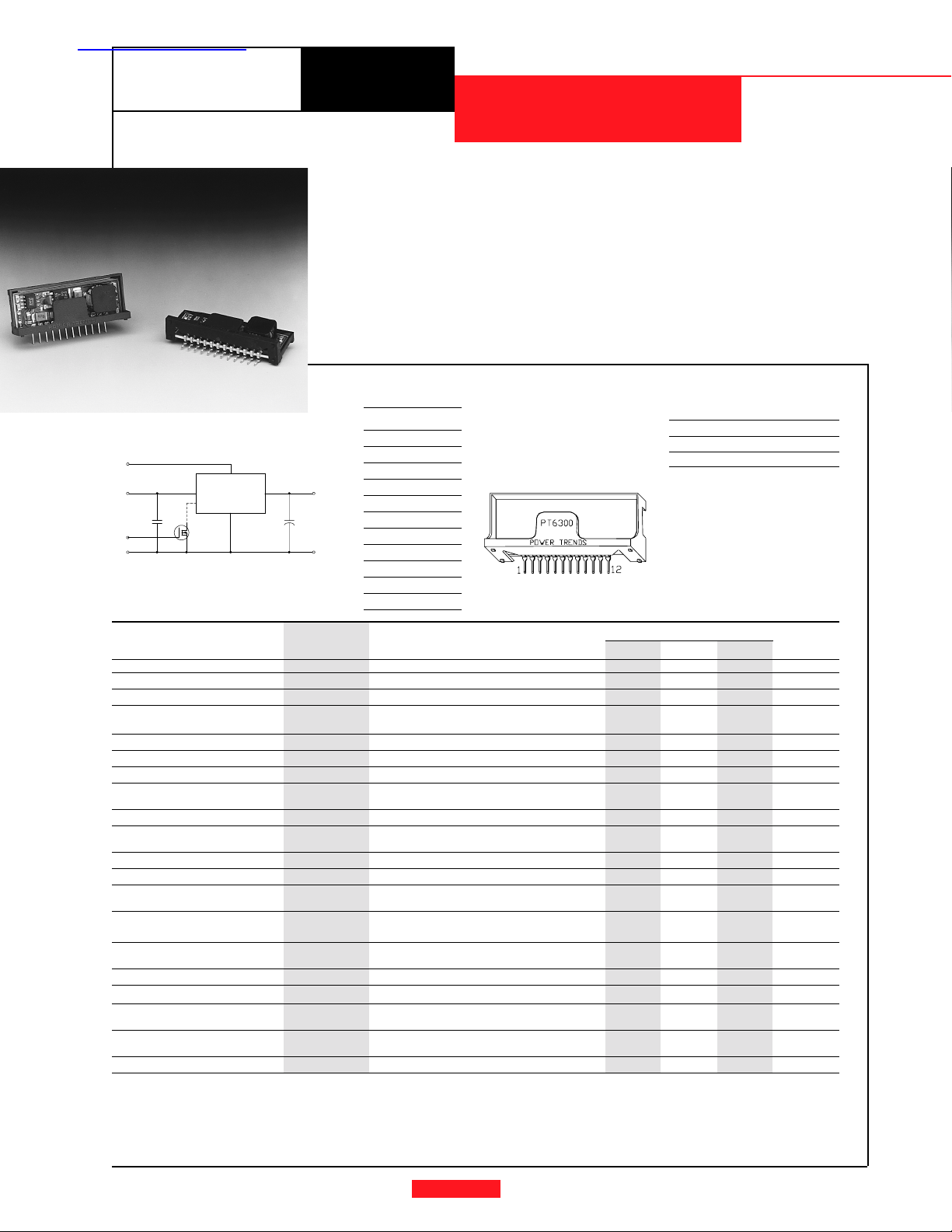
Pin-Out Information
Pin Function
Inhibit
1
(30V max)
2V
Standard Application
VOADJ
V
IN
C1
INH
COM COM
C1 = Optional 1µF ceramic
C2 = Required 100µF electrolytic
Q1 = NFET
12
V
2,3,4
PT6300
1
5,6,7,8
Q1
9,10,11
OUT
+
C2
Specifications
Characteristics
(Ta = 25°C unless noted) Symbols Conditions Min Typ Max Units
Output Current I
Short Circuit Current I
Input Voltage Range V
Output Voltage Tolerance ∆V
Line Regulation Reg
Load Regulation Reg
Vo Ripple/Noise V
Transient Response t
with Co = 100µF V
Efficiency η V
Switching Frequency ƒ
Shutdown Current I
Quiescent Current I
Output Voltage V
Adjustment Range Above V
Absolute Maximum T
Operating Temperature Range
Recommendated Operating T
Temperature Range At Vin = 18V, Io = 2.0A
Thermal Resistance θ
Storage Temperature T
Mechanical Shock Per Mil-STD-883D, Method 2002.3, 1 msec,
Mechanical Vibration Per Mil-STD-883D, Method 2007.2,
Weight — — — 6.5 — grams
* ISR will operate to no load with reduced specifications.
** Input voltage cannot exceed 30V when the inhibit function is used.
Note:
The PT6310 requires a 100µF electrolytic or tantalum output capacitor for proper operation in all applications.
o
sc
in
o
line
load
n
tr
os
o
sc
nl
o
a
a
ja
s
in
3V
in
4V
in
5 GND
6 GND
7 GND
8 GND
9V
out
10 V
out
11 V
out
12 V
out
Adj
Over Vin range 0.1* — 2.0 A
Vin = Vo + 5V — 5.0 — Apk
0.1 ≤ Io ≤ 2.0 A V
Over Vin Range, Io = 2.0 A
Ta = 0°C to +60°C
Over Vin range — ±0.25 ±0.5 %V
0.1 ≤ Io ≤ 2.0 A — ±0.25 ±0.5 %V
V
= V
min, Io = 2.0A — ±2 — %V
in
in
50% load change — 100 200 µSec
Vo over/undershoot — 5.0 — %V
=24V, Io = 2.0 A — 87 — %
in
Over Vin and Io ranges 600 700 800 kHz
Vin = 15V — 100 — µA
Io = 0A, V
Below V
=10V — 10 — mA
in
o
o
Free Air Convection, (40-60LFM)
Free Air Convection (40-60LFM) — 30 — °C/W
— -40 — +125 °C
Half Sine, mounted to a fixture
20-2000 Hz,Soldered in a PC board
Ordering Information
PT6310! = +14.6 Volts
PT6311! = +15.5 Volts
PT6312! = +15.0 Volts
PT6313! = +8.0 Volts
Pkg Style 200
PT6312 only 500 550 600 kHz
Switching Regulator (ISR) designed to
meet the on-board power conversion
needs of battery powered or other equipment requiring high efficiency and
small size. This high performance ISR
offers a unique combination of features
combining 87% typical efficiency with
open-collector on/off control and adjustable output voltage.
Quiescent current in the shutdown
mode is typically less than 100µA.
PT Series Suffix
Case/Pin
Configuration
Vertical Through-Hole
Horizontal Through-Hole
Horizontal Surface Mount
PT6310 Series
4 — 38** V
o +
— ±1.0 ±2.0 %V
See Application Notes.
-40 — +85 °C
-40 — +70
— 500
— 10 — G’s
(PT1234X)
—
SLTS076
(Revised 8/17/99)
N
A
C
o
o
o
o
o
°C
G’s
Power Trends, Inc. 27715 Diehl Road, Warrenville, IL 60555 (800) 531-5782 Fax: (630) 393-6902 http://www.ti.com/powertrends

IMPORTANT NOTICE
T exas Instruments and its subsidiaries (TI) reserve the right to make changes to their products or to discontinue
any product or service without notice, and advise customers to obtain the latest version of relevant information
to verify, before placing orders, that information being relied on is current and complete. All products are sold
subject to the terms and conditions of sale supplied at the time of order acknowledgment, including those
pertaining to warranty, patent infringement, and limitation of liability.
TI warrants performance of its semiconductor products to the specifications applicable at the time of sale in
accordance with TI’s standard warranty. Testing and other quality control techniques are utilized to the extent
TI deems necessary to support this warranty . Specific testing of all parameters of each device is not necessarily
performed, except those mandated by government requirements.
Customers are responsible for their applications using TI components.
In order to minimize risks associated with the customer’s applications, adequate design and operating
safeguards must be provided by the customer to minimize inherent or procedural hazards.
TI assumes no liability for applications assistance or customer product design. TI does not warrant or represent
that any license, either express or implied, is granted under any patent right, copyright, mask work right, or other
intellectual property right of TI covering or relating to any combination, machine, or process in which such
semiconductor products or services might be or are used. TI’s publication of information regarding any third
party’s products or services does not constitute TI’s approval, warranty or endorsement thereof.
Copyright 2000, Texas Instruments Incorporated
 Loading...