

Power Trends PT6305 User Manual
For assistance or to order, call (800) 531-5782
n
n
n
查询PT6305供应商
PT6305 Series
3 AMP HIGH-PERFORMANCE
ADJUSTABLE ISR
• Single-Device 5V to 3V Power
• 85% Efficiency
• Small SIP Footprint:
0.36" x 2.00” x 0.60"(H)
• Wide Input Voltage Range:
+4.5V to +9.0V
• Internal Short Circuit Protection
• Over-Temperature Protection
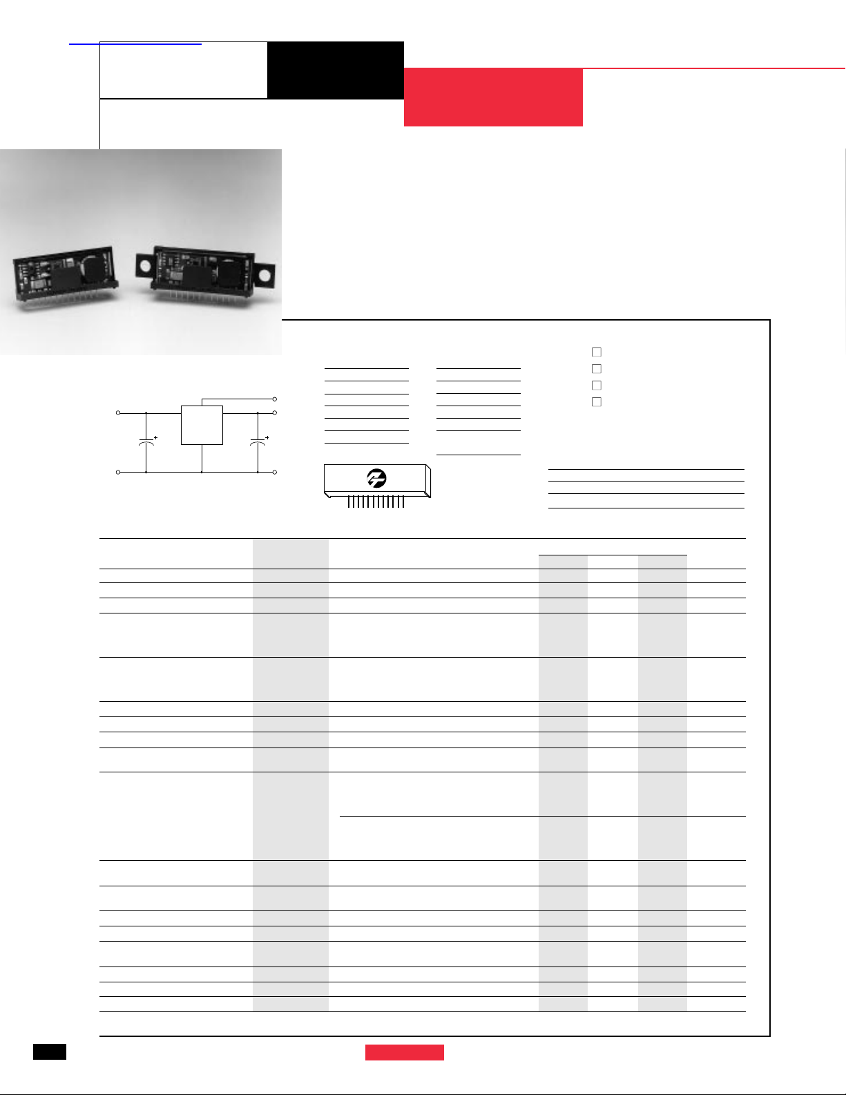
Amp, 12-Pin SIP (Single In-linePackage) Integrated Switching
Regulator (ISR). This high-performance ISR allows easy integration of
low-power 3.3V logic IC’s into existing
5V systems without redesigning the
central power supply. Only one external
capacitor is required for proper
operation. The PT6306,7,8 can be used
The PT6305N is Power Trends’
new high performance +5V to +3.3V, 3
Pin-Out Information
Standard Application
12
VIN
(+)
COM
C1= Optional electrolytic (100µF)
C
= Required 100µF electrolytic (No tantalum)
2
See capacitor application note on page 43.
2,3,4
C1
9,10,11
PT6305,6,7,8
5,6,7,8
Pin No. Function
1 N/C
2 V
VO Adjust
V
OUT
(+)
C2
COM
in
3 V
in
4 V
in
5 GND
6 GND
121
Pin No. Function
7 GND
8 GND
9 V
out
10 V
out
11 V
out
12 Adjust
(See page 40.)
Specifications
Characteristics
(TA=25˚C unless noted) Symbols Conditions Min Typ Max Units
Output Current I
Current Limit I
Short Circuit Current I
Input Voltage Range V
Static Voltage Tolerance V
Line Regulation Reg
Load Regulation Reg
V
Ripple/Noise pk-pk V
o
Transient Response t
with C2= 100µF V
Efficiency
Switching Frequency ƒ
Operating Temperature T
Thermal Resistance θ
Storage Temperature T
Mechanical Shock Per Mil-STD-883D, Method 2002.3 Condition A, 1 msec, Half Sine,
o
cl
sc
in
o
line
load
n
tr
os
η V
o
a
ja
s
mounted to a fixture
Mechanical Vibration Per Mil-STD-883D, Method 2007.2 Condition A, 20-2000 Hz — — 15 G’s
Weight — — — 11.2 — grams
Relative Humidity — Non-condensing 0 — 95 %
*See Thermal Derating chart. **The PT6305 Series can be easily paralleled to provide output current in multiples of 3 amps. Please contact a Power Trends’ Application Engineer for the
appropriate application note.
Note:
The PT6305 Series requires a 100µF electrolytic capacitor for proper operation in all applications.
4.5 ≤ V
≤ VinMAX 0.3 — 3.0** ADC
in
Vin= +5V — 3.6 5.0 ADC
Vin= +5V — 5.0 — Apk
0.3A ≤ Io≤ 3.0A PT6305N 4.5 — 9 VDC
Vin= +5V, Io= 3.0A PT6305N 3.2 3.3 3.4 VDC
0°C ≤ Ta ≤ +70°C PT6306N 1.7 1.8 1.9 VDC
PT6306N 4.5 — 9 VDC
PT6307N 4.5 — 9 VDC
PT6308N 4.5 — 6.0 VDC
PT6307N 2.0 2.1 2.2 VDC
PT6308N 1.1 1.2 1.3 VDC
4.5V ≤ Vin≤ 5.5V, Io= 3.0A — ±25 ±50 mV
Vin= +5V, 0.3 ≤ Io≤ 3.0A — ±25 ±50 mV
Vin= 5V, Io= 3.0A — 66 — mV
Iostep between 1.5A and 3.0A — 200 — µSec
Voover/undershoot — 200 — mV
= +5V, Io= 1.5A PT6305N — 85 — %
in
V
= +5V, Io= 3.0A PT6305N — 80 — %
in
4.5 ≤ V
≤ VinMAX
in
0.3A ≤ Io≤ 3.0A
Free Air Convection (40-60 LFM)
Over V
in and Io
PT6306N — 74 — %
PT6307N — 77 — %
PT6308N — 63 — %
PT6306N — 68 — %
PT6307N — 72 — %
PT6308N — 57 — %
Ranges
Free Air Convection (40-60 LFM) — 25 — °C/W
— -40 — +125 °C
to power high-speed data buses (+2.1V),
or the new GTL (+1.2V) logic buses.
Ordering Information
PT6305n= +3.3 Volts
PT6306
PT6307
PT6308
(For dimensions, see page 66.)
PT Series Suffix
Case/Pin Heat Tab Configuration
Configuration None Side
Vertical Through-Hole
Horizontal Through-Hole
Horizontal Surface Mount
(See Thermal Application Notes on page 44 for heat tab
application data.)
PT6305 SERIES
500 650 800 KHz
0 — +70* °C
— — 500 G’s
= +1.8 Volts
= +2.1 Volts
= +1.2 Volts
(PT1234X)
NR
AG
CB
24
Power Trends, Inc. 27715 Diehl Road, Warrenville, IL 60555 (800) 531-5782 Fax: (630) 393-6902
For assistance or to order, call (800) 531-5782
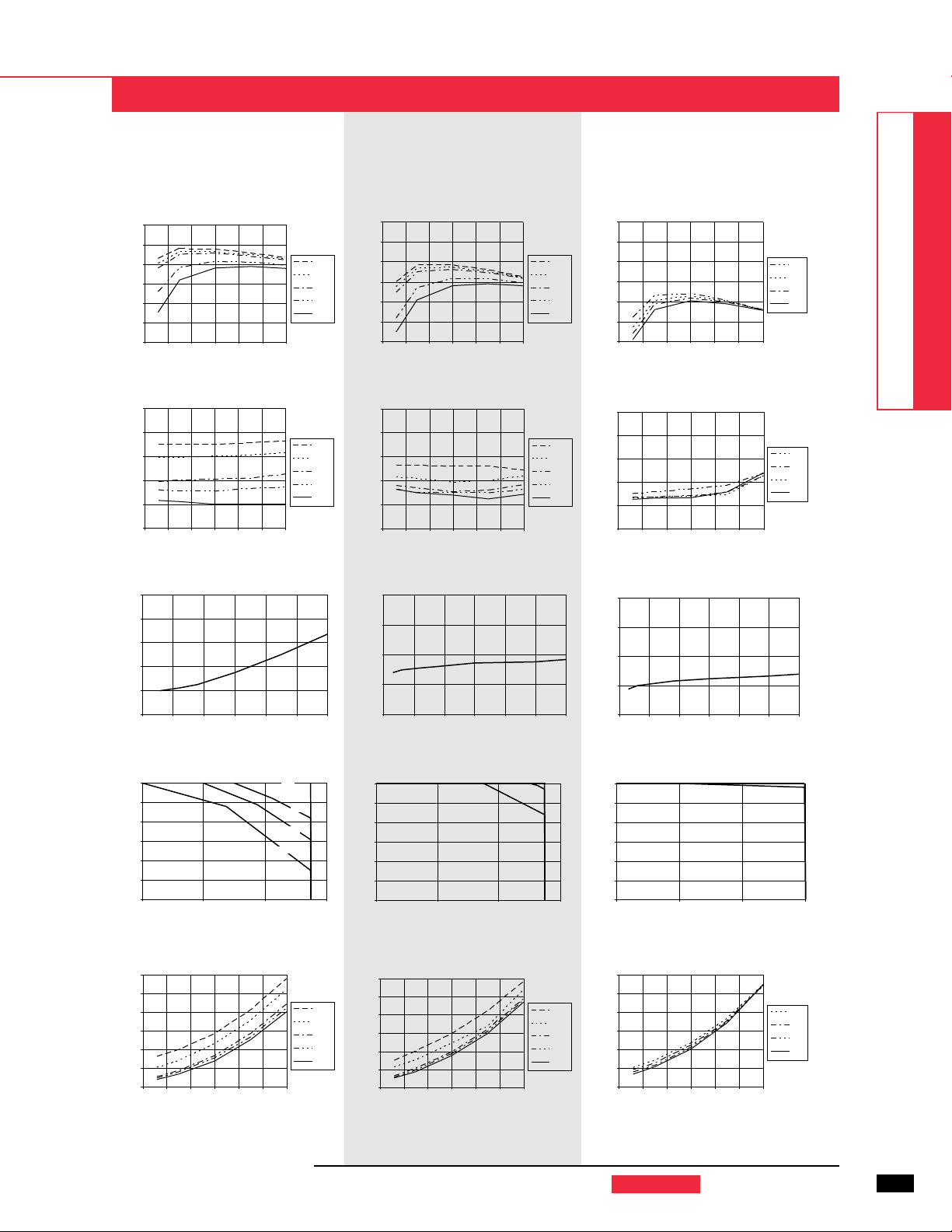
CHARACTERISTIC DATA
PT6305, 3.3 VDC
(See Note 1)
PT6307, 2.1 VDC
(See Note 1)
PT6308, 1.2 VDC
(See Note 1)
Efficiency vs Output Current Efficiency vs Output Current Efficiency vs Output Current
100
90
80
70
60
Efficiency - %
50
40
0 0.5 1 1.5 2 2.5 3
Iout-(Amps)
100
Vin
4.5V
5.0V
5.5V
8.0V
9.0V
90
80
70
60
Efficiency - %
50
40
0 0.5 1 1.5 2 2.5 3
Iout-(Amps)
Vin
4.5V
5.0V
5.5V
8.0V
9.0V
100
90
80
70
60
Efficiency - %
50
40
0 0.5 1 1.5 2 2.5 3
Iout-(Amps)
Ripple vs Output Current Ripple vs Output Current Ripple vs Output Current
100
80
60
40
Ripple-(mV)
20
0
0 0.5 1 1.5 2 2.5 3
Iout-(Amps)
Minimum Input Voltage
4.5
4.3
4.1
3.9
Vin-(Volts)
3.7
3.5
0 0.5 1 1.5 2 2.5 3
Iout-(Amps)
Vin
9.0V
8.0V
5.5V
5.0V
4.5V
(See Note 2) Minimum Input Voltage (See Note 2) Minimum Input Voltage (See Note 2)
100
80
60
40
Ripple-(mV)
20
0
0 0.5 1 1.5 2 2.5 3
4.5
4.25
4
Vin-(Volts)
3.75
3.5
0 0.5 1 1.5 2 2.5 3
Iout-(Amps)
Iout-(Amps)
100
Vin
9.0V
8.0V
5.5V
5.0V
4.5V
80
60
40
Ripple (mv)
20
0
0 0.5 1 1.5 2 2.5 3
4.5
4.25
4
Vin-(Volts)
3.75
3.5
0 0.5 1 1.5 2 2.5 3
Iout-(Amps)
Iout-(Amps)
High-Performance ISRs
DATA SHEETS
Vin
4.5V
5.0V
5.5V
6.0V
Vin
6.0V
5.5V
5.0V
4.5V
Thermal Derating (Ta) (See Note 3) Thermal Derating (Ta) (See Note 3)
3
2.5
2
1.5
1
Iout-(Amps)Pd-(Watts)
0.5
0
4.5 6.5 8.5 10.5
Power Dissipation vs Output Current Power Dissipation vs Output Current Power Dissipation vs Output Current
3
2.5
2
1.5
1
0.5
0
0 0.5 1 1.5 2 2.5 3
Note 1: All data listed in the above graphs, except for derating data, has been developed from actual products tested at 25°C. This data is considered typical data for the ISR.
Note 2: Minimum V
Note 3: Thermal derating graphs are developed in free air convection cooling of 40-60 LFM with no optional heat tab soldered in a printed circuit board. (See Thermal Application Notes).
Vin-(Volts)
Iout-(Amps)
data is typical and is not guaranteed. The data corresponds to a 2% output voltage drop.
in
70°C
85°C
90°C
95°C
Vin
9.0V
8.0V
5.5V
5.0V
4.5V
3
2.5
2
1.5
1
Iout-(Amps)
0.5
0
4.5 6.5 8.5 10.5
3
2.5
2
1.5
1
Pd-(Watts)
0.5
0
0 0.5 1 1.5 2 2.5 3
Vin-(Volts)
Iout-(Amps)
85°C
90°C
95°C
Vin
9.0V
8.0V
5.5V
5.0V
4.5V
Thermal Derating (Ta) (See Note 3)
3
2.5
2
1.5
1
Iout-(Amps)
0.5
0
4.5 5 5.5 6
3
2.5
2
1.5
Pd-(Watts)
1
0.5
0
0 0.5 1 1.5 2 2.5 3
Vin-(Volts)
Iout-(Amps)
90°C
Power Trends, Inc. 27715 Diehl Road, Warrenville, IL 60555 (800) 531-5782 Fax: (630) 393-6902
85°C
Vin
6.0V
5.5V
5.0V
4.5V
25
 Loading...