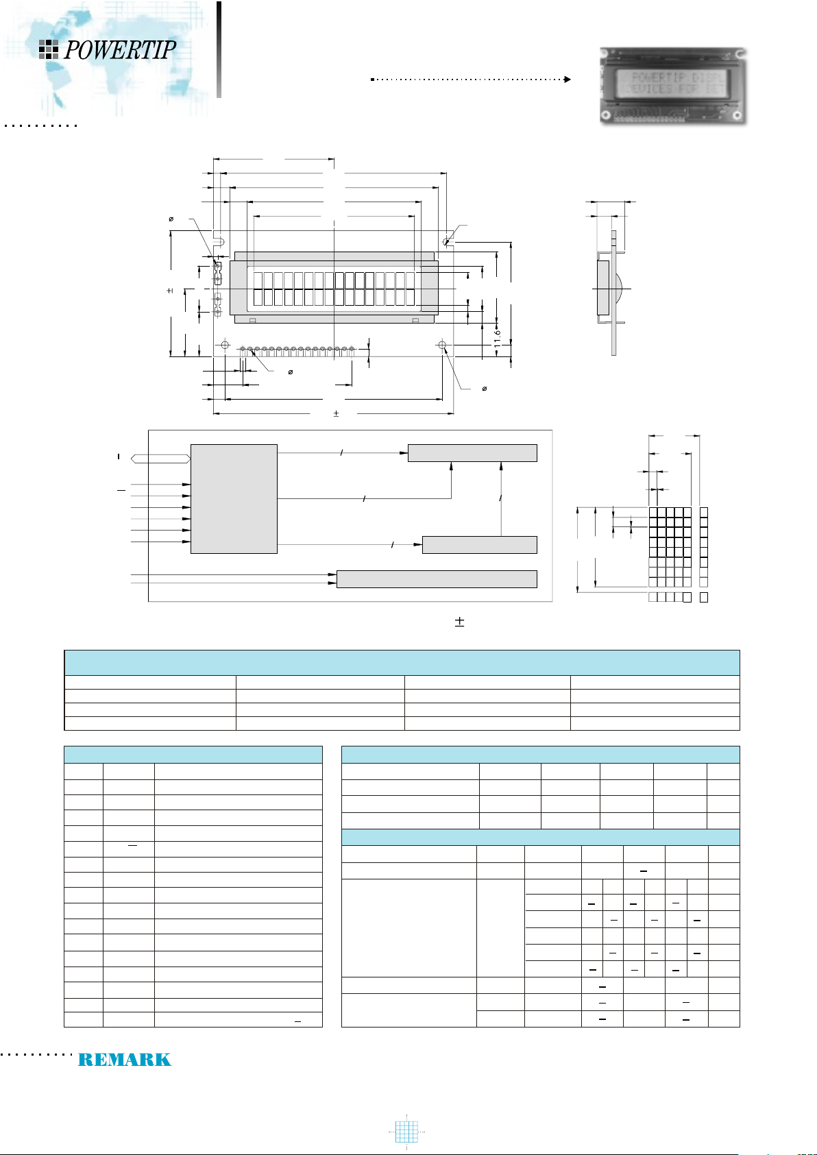
The tolerance unless classified 0.3mm
LCD option: STN, TN, FSTN
Backlight Option: LED,EL Backlight feature, other Specs not available on catalog is under request.
OUTLINE DIMENSION & BLOCK DIAGRAM
MECHANICAL SPECIFICATION
Overall Size
View Area
Dot Size
Dot Pitch
84.0 x 44.0
61.0 x 15.8
0.56 x 0.66
0.60 x 0.70
Module
W /O B/L
EL B/L
Array LED B/L-Edge LED B/L
H2 / H1
5.1 / 9.2
5.1 / 9.2
9.4 / 14.0 - 8.6 / 11.6
Vdd+0.3
V
V
V
13
7
Item
Supply for logic voltage
LCD driving supply voltage
Input voltage
Vdd-Vss
Vdd-Vee
Vin
25
o
C
25
o
C
25
o
C
-0.3
-0.3
-0.3
Symbol
Condition Min.
Max.
Units
ABSOLUTE MAXIMUM RATING
Item
LCD operation voltage
LCM current consumption (No B/L)
Backlight current consumption
Symbol
Min.
Condition
Vop
Idd
LED/edge VB/L=4.2V
LED/array
To p
-20oC
0
o
C
25
o
C
50
o
C
70
o
C
VB/L=4.2V
NW
7.1
4.5
4.1
Vdd=5V
3.8
5.7
6.1
ELECTRICAL CHARACTERISTICS
Typical
NW
Max.
Units
V
5.3
4.9
4.6
7.9
6.7
6.3
V
V
V
V
V
mA
mA
mA
3
NW
7.5
5.1
4.7
4.4
6
6.4
PIN ASSIGNMENT
Pin no. Symbol Function
1
2
3
4
5
6
7
8
9
10
11
12
13
14
Vss
Vdd
Vo
RS
R/W
E
DB0
DB1
DB2
DB3
DB4
DB5
DB6
DB7
Power supply(GND)
Power supply(+)
Contrast Adjust
Register select signal
Data read / write
Enable signal
Data bus line
Data bus line
Data bus line
Data bus line
Data bus line
Data bus line
Data bus line
Data bus line
15
16
A
K
Power supply for LED B/L (+)
Power supply for LED B/L ( )
2
120
40
Power supply voltage
Vdd-Vss
25
o
C
2.7 5.5
V
PC 1602-F
PC 1602-F
3.55
2.96
0.56
0.04
0.04
0.66
5.94
DB7
DB0
E
R/W
RS
V
ss
Vdd
Vo
A
K
LCD
CONTROLLER
LSI
LCD PANEL
COM 16
BACKLIGHT
SEG 40
CONTROL SIGNALS 4
SEG 40
SEGMENT DRIVER
5.56
2-R1.25
25.0
H1
H2
11. 5
15.8
4.1
4.0
36.0
2.15
2- 2.5
16
1
15
76.0
84.0 0.5
16- 1.0
P2.54 x 15=38.1
4.0
10.2
1.8
K
A
14
4- 1.0
1.5
6.0
5.7
2.5
42.2
79.0
73.0
61.0
56.21
44.0 0.5
23.6
15.6
16.0
2.5
 Loading...